Embed Size (px)
Citation preview
A Modular Design Framework for the SystematicDevelopment of Primitive, Application-Specific Optical
Modulation Tools
Nathan Tessema Ersumo
Electrical Engineering and Computer SciencesUniversity of California at Berkeley
Technical Report No. UCB/EECS-2020-180http://www2.eecs.berkeley.edu/Pubs/TechRpts/2020/EECS-2020-180.html
September 16, 2020

Copyright © 2020, by the author(s).All rights reserved.
Permission to make digital or hard copies of all or part of this work forpersonal or classroom use is granted without fee provided that copies arenot made or distributed for profit or commercial advantage and that copiesbear this notice and the full citation on the first page. To copy otherwise, torepublish, to post on servers or to redistribute to lists, requires prior specificpermission.
A Modular Design Framework for theSystematic Development of Primitive,
Application-Specific OpticalModulation Tools
by
Nathan Tessema Ersumo
A report submitted in partial satisfaction
of the requirements for the degree of
Master of Science
Committee:
Professor Rikky Muller, Chair
Professor Laura Waller, Co-Chair
Electrical Engineering and Computer Sciences
University of California, Berkeley
Fall 2020

A Modular Design Framework for the Systematic Development of Primitive, Application-Specific Optical Modulation Tools
by Nathan Tessema Ersumo
Research Project
Submitted to the Department of Electrical Engineering and Computer Sciences, University of California at Berkeley, in partial satisfaction of the requirements for the degree of Master of Science, Plan II. Approval for the Report and Comprehensive Examination:
Committee:
Professor Rikky Muller Research Advisor
(Date)
* * * * * * *
Professor Laura Waller Second Reader
9/4/20
(Date)
09/15/2020

Acknowledgements
First, I would like to thank my partner Nicole Ersaro, who reads every draft I write and tries
(sometimes unsuccessfully) to curb my proclivity for unwieldy sentences. Without her, my
life would be thoroughly mundane. I would also like to thank Cem Yalcin, who turned out
to be an excellent friend on top of being a great research colleague with an infectious level of
enthusiasm throughout this ongoing project. I’m grateful to Anthony Abel, whose enduring
friendship saw us through our undergraduate years at Drexel, our graduate years at Berkeley,
and my wedding to Nicole amidst a pandemic. As always, I would like to thank my parents,
Prof. Tessema Ersumo and Azeb Mulatu, as well as my sister, Amiel Ersumo: their sacrifices
and support are the foundation upon which all of my past and future achievements are built.
On a professional note, I would like to thank Dr. Nick Antipa, Prof. Nicolas Pegard,
Dr. Daniel Lopez, and Prof. Ming Wu for technical contributions, helpful discussions, and
equipment access. I’m grateful to Prof. Laura Waller for access to testing resources and
for serving as a reader for this report. And lastly, I would like to thank my adviser Prof.
Rikky Muller for her ongoing mentorship, support and supervision of this work. Parts of
this report were adapted from [1], a conference proceeding of this work.
Abstract
High-speed primitive optical modulation is widely employed across applications in microscopy,
material processing, adaptive optics and augmented/virtual reality. Despite this ubiquity,
the embodiments of specific optical modulation tools may vary considerably as a result of
the specific performance needs of each application. We present here a consolidated modular
framework for the systemic design of high-speed (≈ 10 kHz) array-based optical modulation
devices requiring limited degrees of freedom (≈ 101−102). The proposed framework combines
a semi-custom commercial fabrication process with a comprehensive simulation pipeline in
order to optimally reconfigure pixel wiring schemes for the efficient allocation of available
degrees of freedom. By decoupling the pixel-level building blocks determining transduction
characteristics from the array-scale partitioning geometry determining overall optical func-
tionality, the framework is able to produce tailored array-scale designs that are both robust
to process variations and easily reconfigurable for adaptation to alternative specifications.
As a demonstration of this framework, phase-shifting piston-motion parallel-plate capacitive
micromirrors were designed and fabricated in small array formats for preliminary assessment
and characterization under MEMSCAP’s standard PolyMUMPs process. Once a suitable
micromirror structure was identified, an axial focusing array with a simulated optical power
range of ±2.89 diopters was subsequently designed via an iterative ring partitioning process
and a Monte Carlo-based simulation pipeline that accounted for experimentally measured
spatial variations in pixel performance.
Table of Contents
List of figures and tables ii
1 Motivation and background 1
2 Proposed modular framework 4
2.1 Technology landscape: key metrics and considerations . . . . . . . . . . . . . 4
2.2 Proposed design methodology . . . . . . . . . . . . . . . . . . . . . . . . . . 7
2.3 Building block selection . . . . . . . . . . . . . . . . . . . . . . . . . . . . . 9
3 Pixel-level design process 12
3.1 Overview of pixel-level computational environment . . . . . . . . . . . . . . 12
3.2 Selected fabrication platform . . . . . . . . . . . . . . . . . . . . . . . . . . . 17
3.3 Assessment of fabricated structures . . . . . . . . . . . . . . . . . . . . . . . 20
4 Array-level design process 23
4.1 The impact of spatial variation . . . . . . . . . . . . . . . . . . . . . . . . . 23
4.2 Overview of array-level computational framework . . . . . . . . . . . . . . . 25
4.3 Simulated performance results . . . . . . . . . . . . . . . . . . . . . . . . . . 30
5 Discussion and conclusions 32
References 34
i

Figures
1.1 Primitive phase shifting profiles . . . . . . . . . . . . . . . . . . . . . . . . . 2
2.1 Flowgraph of micromirror-based design approach . . . . . . . . . . . . . . . 9
3.1 3D rendering of micromirror structure . . . . . . . . . . . . . . . . . . . . . . 13
3.2 Overview of pixel-level simulation results . . . . . . . . . . . . . . . . . . . . 17
3.3 Scanning electron microscopy images of fabricated micromirror structures . . 19
3.4 Assessment of small-format arrays . . . . . . . . . . . . . . . . . . . . . . . . 22
4.1 Performance comparison between shielded, large-format arrays and unshielded,
small-format arrays . . . . . . . . . . . . . . . . . . . . . . . . . . . . . . . . 24
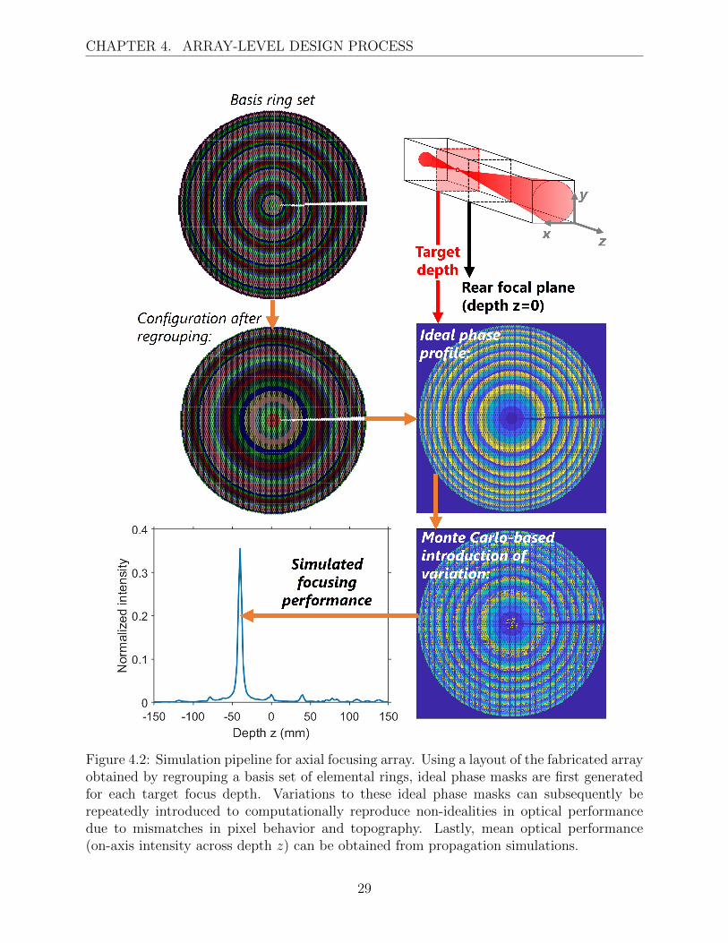
4.2 Simulation pipeline for axial focusing array. . . . . . . . . . . . . . . . . . . 29
4.3 Simulation results for designed axial focusing array . . . . . . . . . . . . . . 31
Tables
2.1 Comparison of high-speed axial focusing technologies . . . . . . . . . . . . . 6
ii
1. Motivation and background
The development of advanced optical techniques in recent years for the recording, manipu-
lation, processing or reproduction of volumetric objects has precipitated a surge of interest
in tools that can dynamically sculpt light. While these needs may broadly be tackled with
full-fledged spatial light modulators (SLMs) that provide arbitrary phase control across a
given plane [2], such tools typically require ≈ 106 addressing channels and offer ≈ 102 Hz
speeds. Full-fledged SLMs are therefore too burdensome or slow for higher speed optical
manipulation that only requires a limited number of degrees of freedom (DoF) [3]. As shown
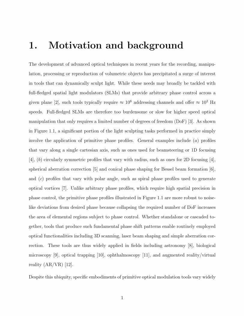
in Figure 1.1, a significant portion of the light sculpting tasks performed in practice simply
involve the application of primitive phase profiles. General examples include (a) profiles
that vary along a single cartesian axis, such as ones used for beamsteering or 1D focusing
[4], (b) circularly symmetric profiles that vary with radius, such as ones for 2D focusing [4],
spherical aberration correction [5] and conical phase shaping for Bessel beam formation [6],
and (c) profiles that vary with polar angle, such as spiral phase profiles used to generate
optical vortices [7]. Unlike arbitrary phase profiles, which require high spatial precision in
phase control, the primitive phase profiles illustrated in Figure 1.1 are more robust to noise-
like deviations from desired phase because collapsing the required number of DoF increases
the area of elemental regions subject to phase control. Whether standalone or cascaded to-
gether, tools that produce such fundamental phase shift patterns enable routinely employed
optical functionalities including 3D scanning, laser beam shaping and simple aberration cor-
rection. These tools are thus widely applied in fields including astronomy [8], biological
microscopy [9], optical trapping [10], ophthalmoscopy [11], and augmented reality/virtual
reality (AR/VR) [12].
Despite this ubiquity, specific embodiments of primitive optical modulation tools vary widely
1
CHAPTER 1. MOTIVATION AND BACKGROUND
Figure 1.1: Primitive phase shifting profiles, including ones that are constant along onecartesian axis, ones that are circularly symmetric, and ones that are radially uniform, are usedin a wide variety of applications across several fields. While the optical functionality enabledwith such phase profiles typically involves some combination of 3D scanning, adaptive opticsor waveform engineering, exact performance needs remain highly application-dependent.
in accordance with the diversity in performance needs across applications: different applica-
tions require different combinations of these fundamental phase modes and different extents
of control for each mode. For instance, while the 3D translation of patterned light generally
requires three DoF, i.e. phase control of the cartesian axis x, cartesian axis y, and polar radius
r, 3D scanning tools cannot easily be adapted for applications with diverging requirements on
resolution and range across X, Y and Z dimensions of the target volume. Accordingly, X−,
Y− and Z−scanning tools tailored for single-cell resolution biological microscopy [13] would
not, for example, efficiently address the macro-scale target volumes of LiDAR surveying [14]
or the axially-compressed aspect ratios of lithography [15]. Moreover, considerations relating
to wavelength of operation and optical power requirements place additional constraints on
2
CHAPTER 1. MOTIVATION AND BACKGROUND
efforts to repurpose existing optical modulation tools. Altogether, the simultaneously preva-
lent and application-specific nature of optical modulation tasks with limited DoF has resulted
in an explosion of off-the-shelf products, from galvanometers [16] and acousto-optic deflec-
tors [17] to tunable lenses [18] and radially curving mirror plates [19], [20], that make use of
various technologies including electrowetting [21], elastomeric deformation [22] , liquid crys-
tals [23], acoustic gradients [24] and micro-electromechanical systems (MEMS) [19]. Though
these myriad commercial offerings and modulation approaches expand available options for
any optical modulation task, off-the-shelf solutions rarely represent the most efficient em-
bodiment of a given task for a given system and application. The application-specific nature
of spatial light modulation tasks often results in inefficiencies for such fixed-format tools,
with either (a) insufficient levels of control and precision being allocated the most critical
DoF, or (b) excess DoF that go wasted and create undesired operating overhead. In order
to provide maximal tailorability for these tools while ensuring accessibility by minimizing
development efforts and cost, we propose a computational framework that allows for the
systematic design or reconfiguration of nimble optical modulation devices requiring limited
DoF by making use of array-based modularity. With this framework, full-fledged arbitrary
spatial light modulation can easily be whittled down into desired application-specific tools by
efficiently consolidating available DoF in a manner that is highly tailored to specific perfor-
mance needs yet minimizes operating overhead. While this framework can be complemented
with any fabrication platform, we illustrate a successful design iteration and experimen-
tally demonstrate the framework’s viability using a standard MEMS fabrication process and
phase-shifting micromirrors as building blocks. A key feature of the proposed framework is
the decoupling of the design and analysis of the unit elements that determine transduction
characteristics from the array-scale geometry that determines overall optical functionality.
With this feature, we anticipate that our framework will power the development of a library
of architectures that can easily be reconfigured and built to specification in the same way
that passive optical elements such as lenses can be custom-fabricated.
3
2. Proposed modular framework
2.1 Technology landscape: key metrics and considera-
tions
To first illustrate how the proposed unified framework can eliminate mismatches, inefficien-
cies, and bottlenecks in optical manipulation systems, we examine key metrics and perfor-
mance tradeoffs at play for one specific example of optical manipulation: dynamic axial
focusing. Two important considerations for this common subtask are that it is often im-
plemented in conjunction with lateral scanning capabilities for 3D scanning [13] and that it
typically introduces target depth-dependent spherical aberrations that require correction [5].
Yet while state-of-the-art lateral scanning tools including galvanometer mirrors and acousto-
optic deflectors boast refresh rates in excess of 5 kHz (under dwelling-capable non-resonant
operation) [25], some of the most widely used and commercially available axial focusing tools
today are not able to match these speeds. Indeed, dynamic optofluidic lenses [26] and liquid
crystal-based devices [27] operate at refresh rates that are well under 300 Hz. Accordingly,
efforts have been made to increase axial focusing speeds to refresh rates of up to 1 MHz
by employing alternative technologies as shown in Table 2.1. But these improvements have
come at the expense of crucial capabilities. Specifically, continuous deformable mirror arrays
(cDMs) [28] and electro-optic deflectors (EODs) [25] require very high voltage drives and/or
numerous addressing channels that entail cumbersome amplifiers, precluding the possibility
of compact driver integration. Furthermore, tunable acoustic gradient index of refraction
(TAG) lenses [24] are continuously sweeping across Z, which means that laser syncing is re-
quired and dwelling is not possible. Alternatively, strategies such as cascading acousto-optic
deflectors (AODs) [25], [29] or producing binary Fresnel zone plates with digital micromir-
4

CHAPTER 2. PROPOSED MODULAR FRAMEWORK
ror devices (DMDs) [30] drastically reduce transmission efficiency. Cascaded AOD systems
also suffer from decreasing dwelling capacity with increasing deflection as well as a limiting
tradeoff between axial and lateral scanning ranges. In addition, monolithic MEMS mirror
plates require resonant-mode operation for meaningful operating ranges, which severely lim-
its performance under dwelling-capable non-resonant modes [20]. And lastly, most of these
approaches to axial focusing provide no additional control over radial phase curvature for a
given target depth, constraining their ability to address target position-dependent aberra-
tions and thereby limiting the ease with which they can be fully adapted to various systems.
5
CHAPTER 2. PROPOSED MODULAR FRAMEWORK
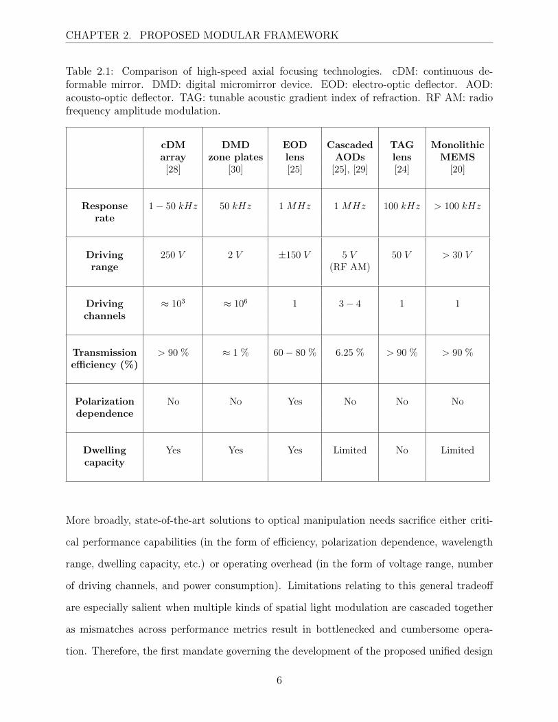
Table 2.1: Comparison of high-speed axial focusing technologies. cDM: continuous de-formable mirror. DMD: digital micromirror device. EOD: electro-optic deflector. AOD:acousto-optic deflector. TAG: tunable acoustic gradient index of refraction. RF AM: radiofrequency amplitude modulation.
cDM DMD EOD Cascaded TAG Monolithicarray zone plates lens AODs lens MEMS[28] [30] [25] [25], [29] [24] [20]
Response 1 − 50 kHz 50 kHz 1 MHz 1 MHz 100 kHz > 100 kHzrate
Driving 250 V 2 V ±150 V 5 V 50 V > 30 Vrange (RF AM)
Driving ≈ 103 ≈ 106 1 3 − 4 1 1channels
Transmission > 90 % ≈ 1 % 60 − 80 % 6.25 % > 90 % > 90 %efficiency (%)
Polarization No No Yes No No Nodependence
Dwelling Yes Yes Yes Limited No Limitedcapacity
More broadly, state-of-the-art solutions to optical manipulation needs sacrifice either criti-
cal performance capabilities (in the form of efficiency, polarization dependence, wavelength
range, dwelling capacity, etc.) or operating overhead (in the form of voltage range, number
of driving channels, and power consumption). Limitations relating to this general tradeoff
are especially salient when multiple kinds of spatial light modulation are cascaded together
as mismatches across performance metrics result in bottlenecked and cumbersome opera-
tion. Therefore, the first mandate governing the development of the proposed unified design
6
CHAPTER 2. PROPOSED MODULAR FRAMEWORK
framework is that operating overhead should be made commensurate to the extent of optical
manipulation that is required: this entails a consolidation process whereby available DoF are
efficiently allotted as part of the framework’s design iteration. The second mandate is that
multiple tools aimed at different tasks and generated from separate design iterations under
this framework can be efficiently cascaded together for expanded performance without the
introduction of performance mismatches. The best way to achieve this feature would be to
introduce modularity to the framework such that tools destined for different tasks can still
comprise identical building blocks that determine transduction characteristics. Overall, the
most straightforward approach to satisfying these two mandates is to structure the proposed
framework as a vector space with an orthogonal basis set of pixels, i.e. unit elements cor-
responding to all available DoF and defined by distinct positions. These unit elements can
then be tiled, consolidated, partitioned and replaced in a systematic way across a prescribed
region that becomes the active area of the designed spatial light modulation tool.
2.2 Proposed design methodology
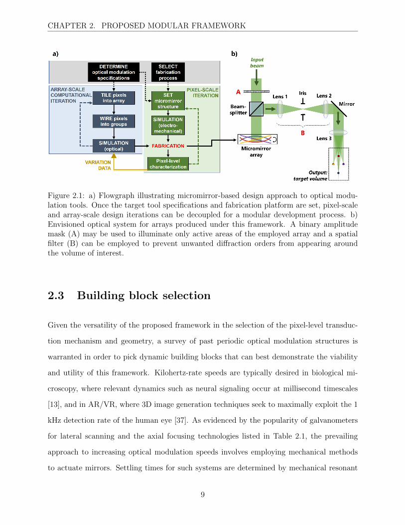
We propose an object-oriented array-format design approach to optical modulation tools
that decouples the building blocks (i.e. pixels) determining transduction characteristics (ex:
applied drive vs. achieved phase shift, settling behavior, etc.), from the array-scale geome-
try determining overall optical functionality as shown in Figure 2.1(a). This modular design
scheme is achieved by fixing the pixel tiling pattern and adjusting grouped wiring schemes
between pixels. Once the pattern and pitch of the array tiling scheme is set, pixels may be
selectively added or removed in accordance with this scheme across a 2D working area that
is agnostic to the unit pixel’s structure. First, such a decoupled analysis strategy between
unit actuator structure and array configuration provides freedom in setting the transduction
mechanism and its balance between spatial uniformity and sensitivity without affecting the
array-level phase coordination strategy that determines optical performance. Depending on
7
CHAPTER 2. PROPOSED MODULAR FRAMEWORK
the application, the unit actuator pixel may be easily switched out within the modular design
framework to structures that rely on particular mechanisms of optical manipulation such as
amplitude modulation [31] or diffraction order-specific phase modulation [32]. Second, com-
pared to larger monolithic structures, partitioning active areas into co-wired grouped regions
and again into small pixels typically provides improved speed and transduction sensitivity
(especially for mechanical structures) [33], the ability to phase-wrap applied patterns for
extended operating ranges, and mitigation against the non-idealities and instabilities that
plague allowable phase modes across larger structures [34], [35]. Third, while segmented
pixels are susceptible to diffraction effects that can introduce unwanted static and dynamic
diffraction orders as well as reduce zeroth-order efficiency commensurately with the square of
array fill factor [36], such segmented arrays can be operated in optical setups that eliminate
these undesired effects via static illumination patterning and spatial filtering as shown in
Figure 2.1(b). Overall, the design process under this framework thus becomes a matter of
iteratively reducing the basis set of addressable elements from an expansive initial orthonor-
mal set representing full-fledged arbitrary spatial light modulation to a reduced set that
eliminates wasted DoF. The only requirement on the selection of pixel building blocks and
fabrication platforms to complement this framework is that they must physically accommo-
date a straightforward and systematic wiring process that mirrors the tiling and partitioning
steps of the computational framework.
8
CHAPTER 2. PROPOSED MODULAR FRAMEWORK
Figure 2.1: a) Flowgraph illustrating micromirror-based design approach to optical modu-lation tools. Once the target tool specifications and fabrication platform are set, pixel-scaleand array-scale design iterations can be decoupled for a modular development process. b)Envisioned optical system for arrays produced under this framework. A binary amplitudemask (A) may be used to illuminate only active areas of the employed array and a spatialfilter (B) can be employed to prevent unwanted diffraction orders from appearing aroundthe volume of interest.
2.3 Building block selection
Given the versatility of the proposed framework in the selection of the pixel-level transduc-
tion mechanism and geometry, a survey of past periodic optical modulation structures is
warranted in order to pick dynamic building blocks that can best demonstrate the viability
and utility of this framework. Kilohertz-rate speeds are typically desired in biological mi-
croscopy, where relevant dynamics such as neural signaling occur at millisecond timescales
[13], and in AR/VR, where 3D image generation techniques seek to maximally exploit the 1
kHz detection rate of the human eye [37]. As evidenced by the popularity of galvanometers
for lateral scanning and the axial focusing technologies listed in Table 2.1, the prevailing
approach to increasing optical modulation speeds involves employing mechanical methods
to actuate mirrors. Settling times for such systems are determined by mechanical resonant
9
CHAPTER 2. PROPOSED MODULAR FRAMEWORK
frequency, which scales with√
km
(where k and m are respectively the spring constant and dy-
namic mass of the actuation mode of interest). By exploiting the surge in resonant frequency
that comes from shrinking down to MEMS scales, micromirror structures can achieve refresh
rates of 10 kHz or higher [33]. Broadly, mirror-based optical tools can be classified into
monolithic structures (ex: galvanometers and varifocal plates) and multi-actuator arrays.
Larger monolithic structures benefit from the simplest driving schemes but provide limited
additional control and often rely on resonant-mode operation due to the high drive required
of DC operation. On the other hand, the expanded functionality offered by multi-actuator
arrays, also known as micromirror arrays or deformable mirror arrays, has drawn considerable
interest which has led to the development of various design iterations over the years [28], [33].
Examples of such iterations have included tip-tilt mirrors for pixel-level beamsteering [38],
piston-motion mirrors for pixel-level phase shifting [39], [40], ribbon-like mirrors that pro-
duce 1D phase profiles [4], and lateral mirror gratings that produce diffraction order-specific
phase shifting [32]. However, uniformity issues relating to spatial variations in fabrication
processing have constrained commercially viable micromirror array designs capable of reli-
able optical modulation to two general subtypes. The first subtype, which corresponds to
the widely employed DMDs, restricts micromirrors to binary operation, i.e. on/off amplitude
modulation, which reduces voltage drive enough to achieve pixel counts on the order of 106
but sacrifices analog control of each pixel [30]. The second subtype, which corresponds to
cDMs, offers analog tip, tilt and piston control by creating highly-rigid suspension schemes
that ensure uniform performance at the expense of inter-actuator coupling and high voltage
drives that reduce viable pixel counts down to ≈ 102 − 103 [41]. Yet since our proposed
framework inherently relies on the averaged performance of hundreds of pixels by consoli-
dating ≈ 103 − 106 pixels per tool into ≈ 101 − 102 actuation channels via co-wiring, the
need for high spatial uniformity is obviated: rigidity and driving voltage requirement can
therefore be relaxed without compromising optical functionality. Accordingly, as part of this
work, we illustrate the pixel-level design process of the framework by designing low-rigidity
10

CHAPTER 2. PROPOSED MODULAR FRAMEWORK
micromirror structures that are best suited for optical modulation tasks requiring limited
DoF. We have chosen piston-based parallel-plate capacitive transduction as the actuation
mechanism for the designed mirror. This mechanism provides full (2π) control over a fun-
damental optical modulation parameter (phase) across a wide range of wavelengths using
a single mechanical deformation mode, simple open-loop DC voltage drive and only one
electrode pair per actuation channel.
11
3. Pixel-level design process
3.1 Overview of pixel-level computational environment
The pixel-level design iteration process involves a preliminary first-order design and analysis
using an analytical framework followed by finite element simulation to assess steady-state
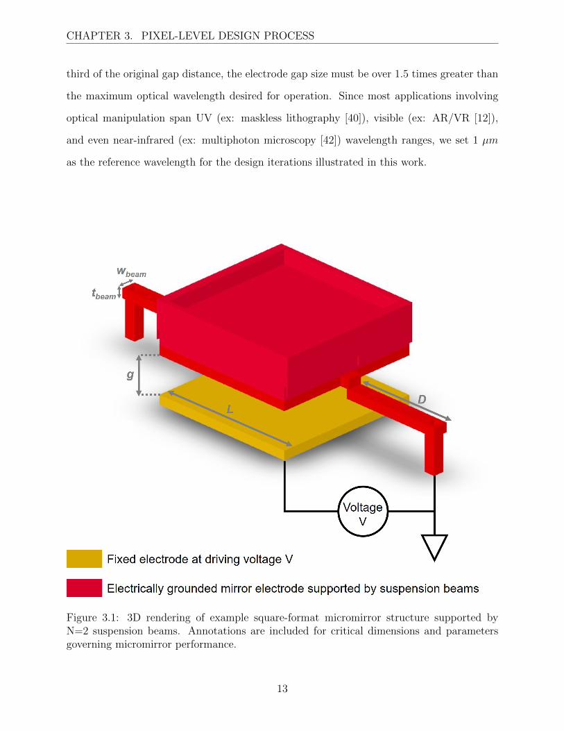
and dynamic transduction behavior. A piston-motion parallel-plate capacitive micromirror
typically involves a mirror body acting as an electrode suspended over a parallel fixed elec-
trode plate with a finite number of suspension beams that are each anchored to the substrate
on one end and attached to the mirror body at the other end, as shown in Figure 3.1. Since
the piston-type mechanical mode only results in the translation of the mirror body along
the direction that is normal to the substrate plane without any torsion, rotation or lateral
motion, the suspension beam is characterized by a guided boundary condition at the mir-
ror end and a clamped boundary condition at the anchor end. Suspension beams must be
arranged such that the net moment experienced by the mirror body is zero: this typically
entails an axially symmetric configuration around the center of the mirror plate. The appli-
cation of a non-zero, positive DC voltage across the two electrodes of the pixel structures
produces an attractive electrostatic force that pulls the suspended mirror body closer to
the fixed electrode. The resulting net displacement of the reflective mirror surface from its
resting plane adds double this displacement value to the travel path of locally incident light,
thus imparting a pixel-level optical phase shift that depends on the light’s wavelength. The
balance between the rigidity, i.e. spring stiffness, of the beams (set by the beams’ geometric
dimensions) and the magnitude of the electrostatic force (set by the parallel plate’s area and
gap size) determine the steady state relationship between displacement and applied voltage.
Since parallel-plate voltage-drive transduction triggers pull-in once displacement exceeds one
12
CHAPTER 3. PIXEL-LEVEL DESIGN PROCESS
third of the original gap distance, the electrode gap size must be over 1.5 times greater than
the maximum optical wavelength desired for operation. Since most applications involving
optical manipulation span UV (ex: maskless lithography [40]), visible (ex: AR/VR [12]),
and even near-infrared (ex: multiphoton microscopy [42]) wavelength ranges, we set 1 µm
as the reference wavelength for the design iterations illustrated in this work.
Figure 3.1: 3D rendering of example square-format micromirror structure supported byN=2 suspension beams. Annotations are included for critical dimensions and parametersgoverning micromirror performance.
13
CHAPTER 3. PIXEL-LEVEL DESIGN PROCESS
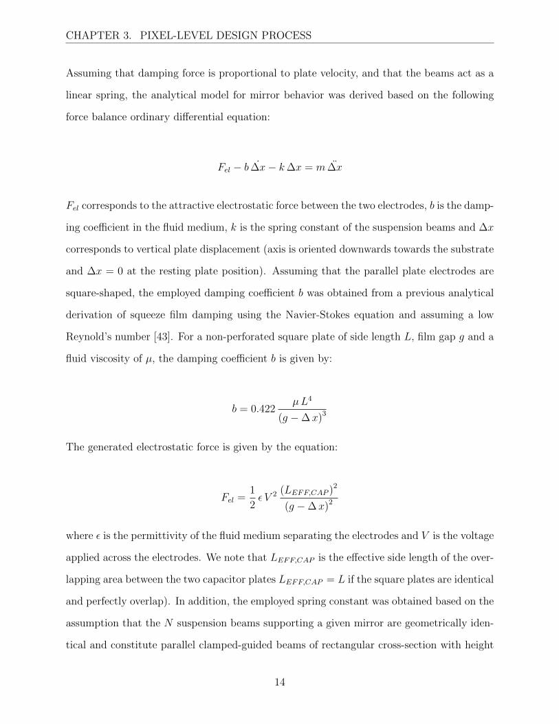
Assuming that damping force is proportional to plate velocity, and that the beams act as a
linear spring, the analytical model for mirror behavior was derived based on the following
force balance ordinary differential equation:
Fel − b ∆x− k∆x = m ∆x
Fel corresponds to the attractive electrostatic force between the two electrodes, b is the damp-
ing coefficient in the fluid medium, k is the spring constant of the suspension beams and ∆x
corresponds to vertical plate displacement (axis is oriented downwards towards the substrate
and ∆x = 0 at the resting plate position). Assuming that the parallel plate electrodes are
square-shaped, the employed damping coefficient b was obtained from a previous analytical
derivation of squeeze film damping using the Navier-Stokes equation and assuming a low
Reynold’s number [43]. For a non-perforated square plate of side length L, film gap g and a
fluid viscosity of µ, the damping coefficient b is given by:
b = 0.422µL4
(g − ∆x)3
The generated electrostatic force is given by the equation:
Fel =1
2ε V 2 (LEFF,CAP )2
(g − ∆x)2
where ε is the permittivity of the fluid medium separating the electrodes and V is the voltage
applied across the electrodes. We note that LEFF,CAP is the effective side length of the over-
lapping area between the two capacitor plates LEFF,CAP = L if the square plates are identical
and perfectly overlap). In addition, the employed spring constant was obtained based on the
assumption that the N suspension beams supporting a given mirror are geometrically iden-
tical and constitute parallel clamped-guided beams of rectangular cross-section with height
14
CHAPTER 3. PIXEL-LEVEL DESIGN PROCESS
tbeam and width wbeam [44]:
k =N E (tbeam)3 wbeam
D3
where D is beam length whereas E is the Young’s modulus of the beam material. This
relationship also holds if the suspension architecture is a single clamped-clamped beam
attached at its midpoint to the mirror body since such a beam is equivalent to two clamped-
guided beams of length D which corresponds to half the length of the full beam. Finally, the
effective mass undergoing acceleration was comprised of the entire mass of the mirror body
(including its reflective metal layer) as well as one third of the mass of the spring beams:
m = ρstructure
(Vmirror body +
N tbeamwbeamD
3
)+ ρmetal Vmetal
where ρstructure is the density of the material forming the beams and mirror body, ρmetal
is the density of the metal used as a reflective layer, Vmirror body is the total volume of the
mirror body, and Vmetal is the total volume of the reflective metal layer. Using the listed
equations, parametric MATLAB scripts were developed to calculate plate displacement over
time for a given applied voltage as well as the required voltage to be applied for a given
displacement. Specifically, ODE45, a numerical Runge Kutta solver, was employed to obtain
mirror behavior after the application of a single step voltage drive from an initial condition
of zero displacement and zero velocity.
Though the described analytical model was used to guide the first-pass selection of design
parameter values (namely pixel-level geometric dimensions), we note that it fails to account
for certain higher-order phenomena that play a significant role in mirror response. Regarding
settling behavior, the analytically obtained damping coefficient b was derived based on the
assumption that there is ambient pressure at the edge of each mirror. Yet given the densely
packed nature of the mirrors across a given array, there will likely be pressure buildup
15
CHAPTER 3. PIXEL-LEVEL DESIGN PROCESS
at mirror edges which may even spill over into surrounding mirrors. More importantly,
the developed model does not incorporate the impact of fringing fields (both within an
isolated mirror and between adjacent mirrors) nor does it recapitulate the true behavior
of the supporting beam, which is a non-linear spring subject to both strain stiffening and
residual stress effects. In addition to modulating spring stiffness and causing suspension
beam buckling, stress mismatches and gradients can also cause suspended mirrors to curl
since a mirror body and its reflective metal layer amount to a bimorph structure. In order
to evaluate the impact of these higher-order effects, design parameters and analyses were
finalized using finite element models constructed in CoventorWare. 3D models of pixels were
constructed by defining fabrication process steps and mask layouts, after which steady state
electromechanical studies, damping studies and eigenfrequency studies were run to obtain
displacement vs. voltage behavior, settling response behavior and mechanical resonance
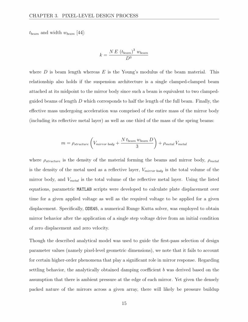
behavior, respectively as shown in Figure 3.2.
16
CHAPTER 3. PIXEL-LEVEL DESIGN PROCESS
Figure 3.2: Overview of simulation results from pixel-level analytical and finite elementsimulation frameworks.
3.2 Selected fabrication platform
Since the pixel-level design process is framed by the imposed constraints and afforded lati-
tudes of the fabrication process, the eventual utility of the proposed computational frame-
work is contingent on the complementary nature of the selected fabrication platform. Specifi-
cally, the chosen fabrication platform must provide a level of accessibility and reliability that
is suitable for systematic redesign as well as a level of versatility and flexibility that can
accommodate the modularity of the framework. To this end, we selected MEMSCAP’s
Multi-User MEMS Processes (MUMPs), specifically the PolyMUMPs standard process in
17

CHAPTER 3. PIXEL-LEVEL DESIGN PROCESS
conjunction with the MUMPs-PLUS semi-custom modification service, to experimentally
illustrate the viability of our framework. Employing PolyMUMPs, a straightforward and
commercial process that involves the deposition of three structure polysilicon layers inter-
leaved with two sacrificial oxide films on a nitride-coated single crystal silicon substrate [45],
will serve to demonstrate that viable micromirror building blocks can be reliably produced
without the need for intricate, advanced, burdensome or costly processing. And with the
addition of the MUMPs-PLUS service, which offers the option of marginal modifications to
layer thicknesses, materials and process sequencing, the base PolyMUMPs fabrication plat-
form is outfitted with a level of tailorability that mirrors the modularity of building blocks
in the design framework. Using this MUMPs-PLUS service, the thickness of the middle
polysilicon layer (Poly1) was reduced from 2 µm down to 500 nm in our fabricated arrays
in order to alleviate micromirror suspension rigidity and reduce voltage drive requirements.
While the described platform provides enough structural versatility to support the develop-
ment of various mechanical suspension, actuation, tiling and wiring schemes, we recognize
that a single standard process step cannot accommodate the wide diversity of application-
specific performance requirements for the mirror surface, including its spectral reflectance,
polarization handling, optical power limit, and sensitivity to angle of incidence. We therefore
envision reflective layer deposition as a separate post-processing step performed in-house or
by a specialized foundry, whereby structures comprising metals, photonic crystals, dielec-
tric stacks or metamaterials are patterned on top of fabricated mirror bodies via techniques
including evaporation [46], sputtering [47], additive manufacturing [48], and e-beam lithog-
raphy [49], [50]. Accordingly, in-house post-processing involving the evaporation and lift-off
patterning of a 250 nm-thick gold layer was performed to impart adequate reflectivity to
our fabricated array pixels. Employing this method instead of the standard 500 nm gold
metal evaporation offered as part of the PolyMUMPs process serves the dual purpose of
illustrating the feasibility of custom post-processing for the deposition of reflective layers
and minimizing the likelihood of mirror curling due to residual stress mismatches.
18
CHAPTER 3. PIXEL-LEVEL DESIGN PROCESS
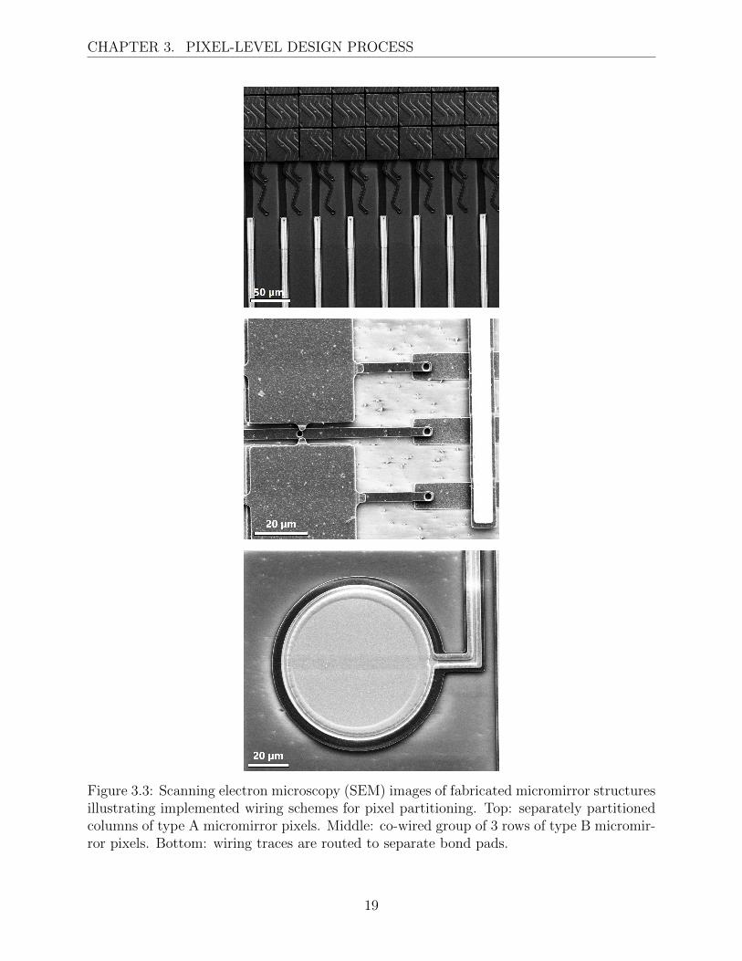
Figure 3.3: Scanning electron microscopy (SEM) images of fabricated micromirror structuresillustrating implemented wiring schemes for pixel partitioning. Top: separately partitionedcolumns of type A micromirror pixels. Middle: co-wired group of 3 rows of type B micromir-ror pixels. Bottom: wiring traces are routed to separate bond pads.
19
CHAPTER 3. PIXEL-LEVEL DESIGN PROCESS
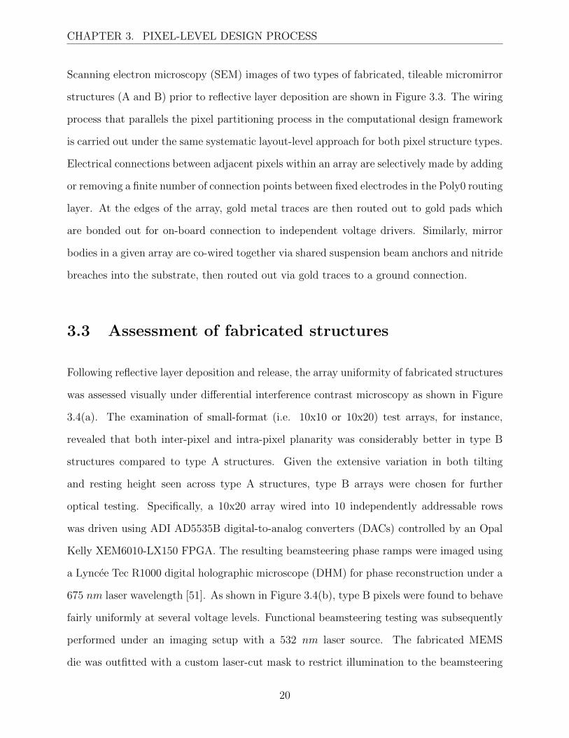
Scanning electron microscopy (SEM) images of two types of fabricated, tileable micromirror
structures (A and B) prior to reflective layer deposition are shown in Figure 3.3. The wiring
process that parallels the pixel partitioning process in the computational design framework
is carried out under the same systematic layout-level approach for both pixel structure types.
Electrical connections between adjacent pixels within an array are selectively made by adding
or removing a finite number of connection points between fixed electrodes in the Poly0 routing
layer. At the edges of the array, gold metal traces are then routed out to gold pads which
are bonded out for on-board connection to independent voltage drivers. Similarly, mirror
bodies in a given array are co-wired together via shared suspension beam anchors and nitride
breaches into the substrate, then routed out via gold traces to a ground connection.
3.3 Assessment of fabricated structures
Following reflective layer deposition and release, the array uniformity of fabricated structures
was assessed visually under differential interference contrast microscopy as shown in Figure
3.4(a). The examination of small-format (i.e. 10x10 or 10x20) test arrays, for instance,
revealed that both inter-pixel and intra-pixel planarity was considerably better in type B
structures compared to type A structures. Given the extensive variation in both tilting
and resting height seen across type A structures, type B arrays were chosen for further
optical testing. Specifically, a 10x20 array wired into 10 independently addressable rows
was driven using ADI AD5535B digital-to-analog converters (DACs) controlled by an Opal
Kelly XEM6010-LX150 FPGA. The resulting beamsteering phase ramps were imaged using
a Lyncee Tec R1000 digital holographic microscope (DHM) for phase reconstruction under a
675 nm laser wavelength [51]. As shown in Figure 3.4(b), type B pixels were found to behave
fairly uniformly at several voltage levels. Functional beamsteering testing was subsequently
performed under an imaging setup with a 532 nm laser source. The fabricated MEMS
die was outfitted with a custom laser-cut mask to restrict illumination to the beamsteering
20

CHAPTER 3. PIXEL-LEVEL DESIGN PROCESS
array, and placed at the front focal plane of a 100 mm focal length lens, with a CMOS
camera positioned at the rear focal plane. Phase ramps were subsequently produced at
steps of 0, π4, π
3, and π (i.e. mirror displacement increments of 0 nm, 33 nm, 44 nm, and
133 nm). While the small array format represents a narrow Fourier bandwidth resulting in
poor resolution and limited beamsteering performance, the test array was able to successfully
and incrementally deflect the zeroth order diffraction spot generated at the camera plane as
shown in Figure 3.4(c).
Most notably, producing a phase ramp with a pixel step of π resulted in a deflected spot
located halfway between the zeroth order (DC) and first order diffraction spots under uni-
form phase (i.e. no voltage drive), consistent with the behavior of a binary phase grating.
Altogether, this pixel-level development iteration illustrates how the described micromir-
ror design process can be coupled with a standard fabrication platform to produce several
small-format arrays, rapidly triage potential building blocks for suitability via inspection and
simple functional tests, and perform pixel-level characterization measurements to inform the
array-scale design process.
21
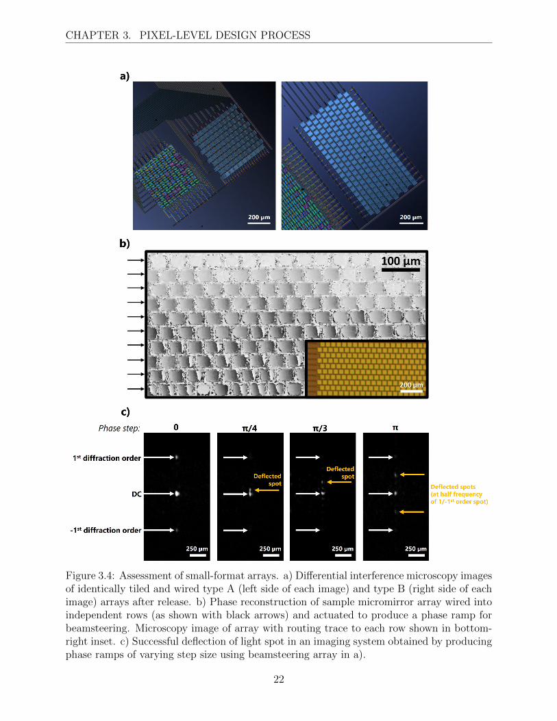
CHAPTER 3. PIXEL-LEVEL DESIGN PROCESS
Figure 3.4: Assessment of small-format arrays. a) Differential interference microscopy imagesof identically tiled and wired type A (left side of each image) and type B (right side of eachimage) arrays after release. b) Phase reconstruction of sample micromirror array wired intoindependent rows (as shown with black arrows) and actuated to produce a phase ramp forbeamsteering. Microscopy image of array with routing trace to each row shown in bottom-right inset. c) Successful deflection of light spot in an imaging system obtained by producingphase ramps of varying step size using beamsteering array in a).
22
4. Array-level design process
4.1 The impact of spatial variation
While the pixel-level design process provides insight into expected performance and relative
strengths and weaknesses across various structures, spatial process variations during fabrica-
tion are often so significant that pixel-level simulations alone cannot reliably guide array-scale
design. Experimental post-fabrication pixel-level characterization is therefore typically nec-
essary in order to factor in non-uniformities in pixel performance and accurately predict
functional optical performance. The extent to which such variations can lead to deviations
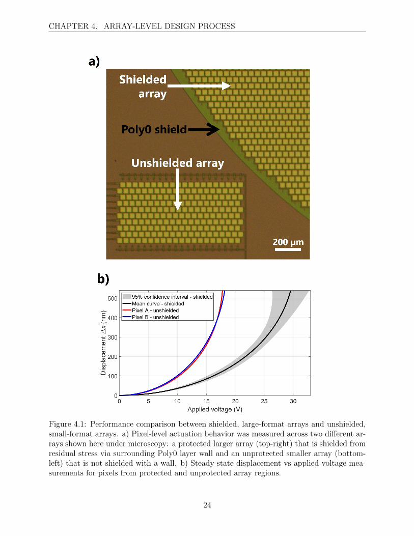
in pixel performance is illustrated in Figure 4.1. As seen in Figure 4.1(a), two arrays were
laid out and fabricated next to each other, the first one being a large 8.2 mm diameter
circular array surrounded by a wall of Poly0 for residual stress shielding, and the second one
being a smaller, unshielded 480 µm × 960 µm array. Steady state voltage vs displacement
measurements performed across pixels of both arrays under DHM and shown in Figure 4.1(b)
reveal two kinds of variations. First, spatially continuous variations in geometric properties
including layer thicknesses result in regional variations in pixel performance, as evidenced
by the wide 95 % confidence interval margins of the larger array and the comparatively uni-
form pixel performance across the smaller array. Second, non-periodic structures that are
peripheral to fabricated arrays (ex: routing traces, shielding walls, substrate breaches and
die edges) can significantly modulate the extent and impact of residual stress mismatches.
For instance, the observed difference between the 30.4 V mean pull-in voltage of the larger
array and the 18.3 V mean pull-in voltage of the smaller array can be attributed to the
fact that stress shielding mitigates spring stiffening or softening of the suspension beams in
Poly1, which experiences a nominal compressive stress of −10 MPa [45].
23
CHAPTER 4. ARRAY-LEVEL DESIGN PROCESS
Figure 4.1: Performance comparison between shielded, large-format arrays and unshielded,small-format arrays. a) Pixel-level actuation behavior was measured across two different ar-rays shown here under microscopy: a protected larger array (top-right) that is shielded fromresidual stress via surrounding Poly0 layer wall and an unprotected smaller array (bottom-left) that is not shielded with a wall. b) Steady-state displacement vs applied voltage mea-surements for pixels from protected and unprotected array regions.
24
CHAPTER 4. ARRAY-LEVEL DESIGN PROCESS
Overall, these disparities in pixel performance were experimentally captured under DHM
with two types of measurements: variations in resting pixel surface height, which were found
to have a standard deviation of 13.83 nm, and variations in actuation-dependent behavior,
which were found to have an integrated mean standard deviation of 53.26 nm. The intra-
pixel topography of micromirrors was measured under non-contact atomic force microscopy
to have a standard deviation of 0.6 nm across 1 µm × 1 µm unit areas (relevant to target
laser wavelength scales) and was thus found to be negligible at the scale of array-wide
functional performance. Therefore, while pixel-level simulation results are sufficient for first-
pass array-scale design iterations under idealized assumptions, porting these quantifications
of pixel non-uniformity into refined later-stage iterations is crucial to assessing whether the
averaging effect of pixel grouping can realistically overcome such non-idealities and ensure
adequate optical performance.
4.2 Overview of array-level computational framework
The array-scale design framework was implemented using MATLAB’s Image Processing Tool-
box as an optical system consisting of an offset lens with the micromirror array plane posi-
tioned at the front focal plane and with the target/output volume centered around the rear
focal plane. In order to construct an optical test setup that is tailored to a given target appli-
cation for pertinent simulation results, several system-level parameters must first be defined
at the start of any design iteration. These parameters include the focal length f of the offset
lens as well as the wavelength λ and complex amplitude profile (ex: Gaussian vs uniform,
normally incident vs oblique, amplitude mask defining aperture, etc.) of the coherent illumi-
nation striking the active area of the micromirror array. Under this framework, the process
of designing the partitioning geometry that determines optical functionality involves making
iterative manipulations to an amplitude mask matrix representing the micromirror array.
This matrix is first constructed as a binary 2D image of all potential micromirror pixels that
25
CHAPTER 4. ARRAY-LEVEL DESIGN PROCESS
may be placed in the active region of interest in accordance with the tiling scheme defined by
the pixel-level design process and at a resolution (i.e. matrix element size) that is compara-
ble to the wavelength of interest (≈ 1 µm). A segmentation function returning the set of all
8-connected objects in a binary image is subsequently employed to expand the original image
into separate matrices of identical size isolating each micromirror pixel. Each of these pixels
may then be kept or removed from the active area via simple matrix addition/subtraction op-
erations. Additionally, object dilation and erosion operations may be used to adjust pixel fill
factor, and pixel grouping indicative of co-wiring and joint actuation is performed by adding
distinct single-pixel matrices together. Once a pixel partitioning iteration culminates in a
finite number n of matrices, each corresponding to an independently addressable actuation
channel, mirror efficiency can be accounted for by scaling these matrices, and therefore the
unit amplitudes denoting active pixel regions, with the experimentally measured reflectance
of the chosen pixel mirror surface at the wavelength of interest. Background array reflectiv-
ity may also be incorporated into the framework by constructing a separate static matrix
with a non-zero complex amplitude across non-mirror regions and with null amplitudes in
all active mirror regions. Lastly, in order to simulate optical performance for a given phase
mask produced by the array, active single-channel matrices are multiplied by their respective
exponential phase factors and summed together along with the static background reflection
matrix. The resulting complex matrix is then subjected to a 2D fast Fourier transform
(FFT) operation and scaled in accordance with Parseval’s theorem to obtain the complex
amplitude profile at the rear focal plane of the lens (the matrix’s unit element dimensions
are also scaled by a factor λ f). Fresnel propagation may then be employed to obtain the
complex amplitude profile of any plane that is both parallel and proximal to the rear focal
plane: this feature is implemented via pre-multiplication by a Fresnel propagation kernel
prior to the FFT operation in order to avoid the computational burden of an additional
convolution operation in the framework.
To further illustrate the developed array-scale framework along with its capacity to assess
26
CHAPTER 4. ARRAY-LEVEL DESIGN PROCESS
process variation impacts, we present in this work a full design iteration targeting axial fo-
cusing as shown in Figure 4.2. Given that axial focusing requires only radial phase control
in order to produce spherical phase profiles at the micromirror plane, we have simplified
the design process by pre-partitioning array pixels into 45 elemental rings of identical track
width. Since the ADI AD5535B DAC chosen to drive the array has a total of 32 independent
channels, designing the axial focusing array becomes a matter of finding the optimal regroup-
ing scheme that consolidates these 45 elemental rings into the 32 rings that determine the
final pixel partitioning geometry. The quality of a given partitioning geometry is evaluated
by examining focusing performance, as measured by peak optical intensity profile across the
full depth range of the output volume, for several phase masks targeting different depths.
For a certain target depth at a signed distance dz from the rear focal plane of the offset lens,
the phase shift ∆φ required at an array ring bounded by radii a and b (a < b) is given by:
∆φ =1
b− a
∫ b
a
2 π f 2
dz λ
1 −
√1 − (dz r)
2
f 4
d r + φ
where φ is some global phase offset applied uniformly to all rings.
Similarly, in the case of 1D beamsteering along a certain axis x at the rear focal plane,
for a target lateral deflection to a signed distance dx from the optical axis, the phase shift
∆φ required at an array band bounded by coordinates e and f (e < f) along the relevant
cartesian axis would be given by:
∆φ =1
f − e
∫ f
e
−2πdxλ f
x dx+ φ = −π dxλ f
(e+ f) + φ
Importantly, one of the most useful features of the described array-scale framework is its
ability to incorporate the impact of process variations into simulated performance based
on a priori experimentally-obtained distribution data for the chosen pixel structures. This
27
CHAPTER 4. ARRAY-LEVEL DESIGN PROCESS
is achieved in a Monte Carlo-based approach where deviations to phase values across the
array are introduced by generating random numbers using measured distribution param-
eters, namely standard deviation (assuming normality for simplicity). Once this process
has been repeatedly performed in order to construct several non-ideal phase profiles that
are representative of what may be produced by actual fabricated arrays for a given target
depth, computational simulations of optical propagation through the system are performed
to obtain mean optical performance and expected deviation ranges.
We note that, for the fabricated pixel structures, actuation-dependent displacement devia-
tions that vary with applied phase dominate over static variations, as illustrated in Figure
4.2 by the fact that rings imparting greater phase shifts are subject to greater phase hetero-
geneity. Given such behavior, modulating the global phase offset parameter φ to minimize
mean actuation across all channels can be useful in improving focusing performance for a
given target depth. In addition, as part of this same phase modulation process, applied
phases may be constrained to a finite set of discrete values in order to account for driver
quantization. While the ADI AD5535B DACs used in this work are capable of 14-bit drive
and thus a millivolt-scale precision that is eclipsed by the actuation-dependent variation
exhibited by the employed pixel structures, other design iterations may be constrained by
driving schemes of lower bit-depth and therefore significant quantization effects.
28
CHAPTER 4. ARRAY-LEVEL DESIGN PROCESS
Figure 4.2: Simulation pipeline for axial focusing array. Using a layout of the fabricated arrayobtained by regrouping a basis set of elemental rings, ideal phase masks are first generatedfor each target focus depth. Variations to these ideal phase masks can subsequently berepeatedly introduced to computationally reproduce non-idealities in optical performancedue to mismatches in pixel behavior and topography. Lastly, mean optical performance(on-axis intensity across depth z) can be obtained from propagation simulations.
29
CHAPTER 4. ARRAY-LEVEL DESIGN PROCESS
4.3 Simulated performance results
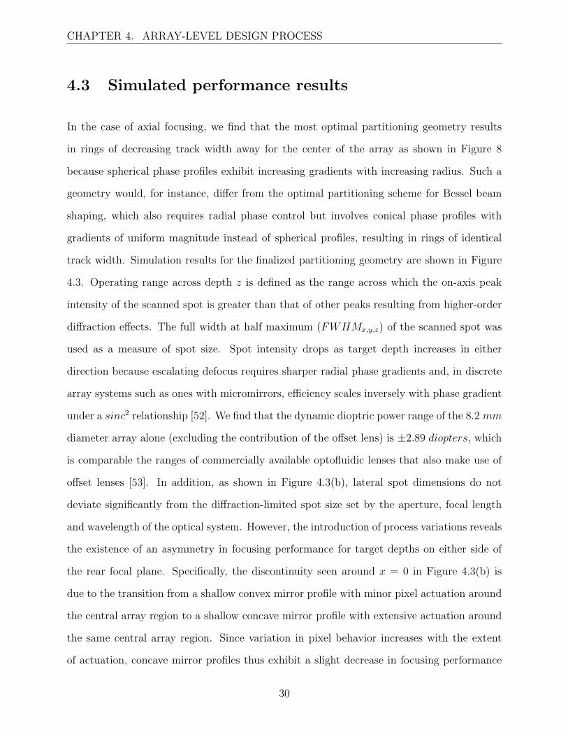
In the case of axial focusing, we find that the most optimal partitioning geometry results
in rings of decreasing track width away for the center of the array as shown in Figure 8
because spherical phase profiles exhibit increasing gradients with increasing radius. Such a
geometry would, for instance, differ from the optimal partitioning scheme for Bessel beam
shaping, which also requires radial phase control but involves conical phase profiles with
gradients of uniform magnitude instead of spherical profiles, resulting in rings of identical
track width. Simulation results for the finalized partitioning geometry are shown in Figure
4.3. Operating range across depth z is defined as the range across which the on-axis peak
intensity of the scanned spot is greater than that of other peaks resulting from higher-order
diffraction effects. The full width at half maximum (FWHMx,y,z) of the scanned spot was
used as a measure of spot size. Spot intensity drops as target depth increases in either
direction because escalating defocus requires sharper radial phase gradients and, in discrete
array systems such as ones with micromirrors, efficiency scales inversely with phase gradient
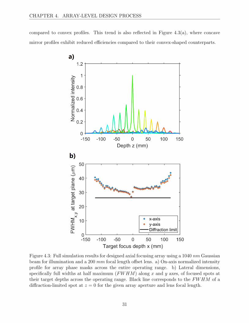
under a sinc2 relationship [52]. We find that the dynamic dioptric power range of the 8.2 mm
diameter array alone (excluding the contribution of the offset lens) is ±2.89 diopters, which
is comparable the ranges of commercially available optofluidic lenses that also make use of
offset lenses [53]. In addition, as shown in Figure 4.3(b), lateral spot dimensions do not
deviate significantly from the diffraction-limited spot size set by the aperture, focal length
and wavelength of the optical system. However, the introduction of process variations reveals
the existence of an asymmetry in focusing performance for target depths on either side of
the rear focal plane. Specifically, the discontinuity seen around x = 0 in Figure 4.3(b) is
due to the transition from a shallow convex mirror profile with minor pixel actuation around
the central array region to a shallow concave mirror profile with extensive actuation around
the same central array region. Since variation in pixel behavior increases with the extent
of actuation, concave mirror profiles thus exhibit a slight decrease in focusing performance
30
CHAPTER 4. ARRAY-LEVEL DESIGN PROCESS
compared to convex profiles. This trend is also reflected in Figure 4.3(a), where concave
mirror profiles exhibit reduced efficiencies compared to their convex-shaped counterparts.
Figure 4.3: Full simulation results for designed axial focusing array using a 1040 nm Gaussianbeam for illumination and a 200 mm focal length offset lens. a) On-axis normalized intensityprofile for array phase masks across the entire operating range. b) Lateral dimensions,specifically full widths at half maximum (FWHM) along x and y axes, of focused spots attheir target depths across the operating range. Black line corresponds to the FWHM of adiffraction-limited spot at z = 0 for the given array aperture and lens focal length.
31
5. Discussion and conclusions
Overall, the described pixel-scale and array-scale computational frameworks offer a modular,
systematic and efficient path for both de novo design iterations and adaptive reconfigura-
tions of pixel-based primitive spatial light modulation tools. At the core of our development
approach is an iterative pixel partitioning process for grouped pixel drive that offers two
advantages: an alleviation of operating burden via tailored consolidation of drive channels,
and a pixel averaging effect that rescues optical functionality in the face of significant spatial
process variation. Through a development process interweaving simulation-based design and
experimental characterization, we also demonstrate that both viable pixel-level structures
and competitive array-scale optical modulation tools (such as ones for axial focusing) can
feasibly be constructed from standard, widely accessible fabrication processes with off-the-
shelf drivers boasting channel counts on the order of ≈ 101. The proposed development
approach to optical modulation tools also has bearings on the design of complex optical
manipulation systems involving multiple tools: the allotment of required DoF can indeed
be re-envisioned to allow for more compact driving schemes under cascaded operation. For
instance, by recognizing that axial defocusing can be achieved by cascading cylindrical fo-
cusing along two orthogonal directions, a 3D scanning system may be constructed with two
identical ribbon-partitioned arrays (one array for X-axis steering and cylindrical focusing,
followed by another array rotated by 90◦ for Y-axis steering and cylindrical focusing) in-
stead of three arrays (one for X-axis steering, a second for Y-axis steering, and a third for
axial focusing) [4]. Thus, with such system-level considerations, complex light manipulation
systems can be assembled from a minimal number of primitive optical modulation tools for
even greater reductions in total number of drive channels.
A number of insights and potential improvements can be gleaned from the design iteration
32
CHAPTER 5. DISCUSSION AND CONCLUSIONS
endeavored in this work. First, the use of pixelated, spatially discrete phased arrays as active
areas instead of continuous phase surfaces alters efficiency behavior. Peak efficiency for a
given array becomes set not only by the reflectivity of the mirror surface, but also by the
square of the array’s pixel fill factor. Efficiency then drops off from this maximum value in a
sinc2 fashion as phase gradient increases, i.e. as the extent of optical modulation/deflection
increases. The altered behavior must be accounted for with performance margins in both
pixel-level and array-level designs across applications that impose uniformity or threshold
constraints on efficiency. Second, since the proposed tools rely on co-wired pixel operation,
it is imperative that a single-pixel failure event such as electrode shorting does not result
in whole-channel failure. Accordingly, fail-safe mechanisms such as gap stop structures and
insulating barriers are crucial to the pixel-level design process: once isolated properly, a
single-pixel failure typically results in negligible degradation to array-scale performance due
to pixel averaging. Third, power handling, which is a critical aspect of desired performance
in some applications including laser micro-machining [54], was not addressed in the reported
design iteration and experimental characterization. A survey of the literature reveals that
micromirrors are susceptible to reflectance losses due to eutectic bond widening as well as
mirror delamination due to gaseous release at the temperatures experienced under high opti-
cal powers [46]. While an extrapolation of previously reported optical power limits measured
across PolyMUMPS micromirrors suggests that our designed arrays should be able to with-
stand over 10 W without sustaining permanent damage [46], opto-thermal analyses and
characterizations would be required as part of this design process for an accurate assessment
of power handling.
We identify a number of future opportunities that can expand the features and capabilities
of both the described framework and the resulting array-based tools. While the frame-
work’s current embodiment models process variations as being normally distributed and
uncorrelated noise-like phase fluctuations, improved simulation results and design processes
may be obtained by modeling these variations more accurately as location-dependent phase
33
CHAPTER 5. DISCUSSION AND CONCLUSIONS
deviations given that the underlying parameters driving these non-uniformities in pixel per-
formance, namely layer thicknesses and residual stress levels, exhibit regional continuity.
Though such an approach entails more comprehensive characterizations of process variation
post-fabrication, it also offers a path to enhanced optical performance via regional parti-
tioning schemes that allow for channel-specific calibration and correction. Moreover, fab-
ricated tools may be outfitted with limited dynamic runtime rewiring capabilities through
the placement of active electrical routing structures composed of electromechanical relays
(akin to cross-connect architectures) outside of the array region for multi-mode operation
using the same number of driving channels [55]. Finally, for applications that exhibit tem-
poral integration and averaging such as AR/VR [12], global phase offsets may be modulated
across several frames to improve optical performance by washing out artifacts resulting from
unwanted diffraction effects or actuation-dependent process variations.
34

References
[1] N. T. Ersumo, C. Yalcin, N. Antipa, N. Pegard, L. Waller, D. Lopez, and R. Muller,
“Design framework for high-speed 3d scanning tools and development of an axial fo-
cusing micromirror-based array,” MOEMS and Miniaturized Systems XIX, SPIE Opto,
2020.
[2] T. W. Clark, R. F. Offer, S. Franke-Arnold, A. S. Arnold, and N. Radwell, “Comparison
of beam generation techniques using a phase only spatial light modulator,” Optics
express, vol. 24, no. 6, pp. 6249–6264, 2016, issn: 1094-4087.
[3] Z. Zhang, Z. You, and D. Chu, “Fundamentals of phase-only liquid crystal on silicon
(lcos) devices,” Light: Science & Applications, vol. 3, no. 10, e213–e213, Oct. 24, 2014,
issn: 2047-7538. doi: 10.1038/lsa.2014.94.
[4] J. R. Landry, S. S. Hamann, and O. Solgaard, “Random access cylindrical lensing and
beam steering using a high-speed linear phased array,” IEEE Photonics Technology
Letters, vol. 32, no. 14, pp. 859–862, 2020, issn: 1041-1135.
[5] P. S. Salter and M. J. Booth, “Adaptive optics in laser processing,” Light: Science &
Applications, vol. 8, no. 1, pp. 1–16, 2019, issn: 2047-7538.
[6] C. Rodrıguez, Y. Liang, R. Lu, and N. Ji, “Three-photon fluorescence microscopy with
an axially elongated bessel focus,” Optics letters, vol. 43, no. 8, pp. 1914–1917, 2018,
issn: 1539-4794.
[7] S.-W. Cho, H. Kim, J. Hahn, and B. Lee, “Generation of multiple vortex-cones by
direct-phase modulation of annular aperture array,” Applied Optics, vol. 51, no. 30,
pp. 7295–7302, 2012, issn: 2155-3165.
35
REFERENCES
[8] S. A. Matthews, M. Collados, M. Mathioudakis, and R. Erdelyi, “The european so-
lar telescope (est),” Ground-based and Airborne Instrumentation for Astronomy VI,
vol. 9908, p. 990 809, 2016.
[9] V. Emiliani, A. E. Cohen, K. Deisseroth, and M. Hausser, “All-optical interrogation
of neural circuits.,” The Journal of neuroscience : the official journal of the Society
for Neuroscience, vol. 35, no. 41, pp. 13 917–26, Oct. 14, 2015, issn: 1529-2401. doi:
10.1523/JNEUROSCI.2916-15.2015.
[10] Y. Liang, Y. Cai, Z. Wang, M. Lei, Z. Cao, Y. Wang, M. Li, S. Yan, P. R. Bianco,
and B. Yao, “Aberration correction in holographic optical tweezers using a high-order
optical vortex,” Applied optics, vol. 57, no. 13, pp. 3618–3623, 2018, issn: 2155-3165.
[11] Y. Zhang, S. Poonja, and A. Roorda, “Mems-based adaptive optics scanning laser
ophthalmoscopy,” Optics letters, vol. 31, no. 9, pp. 1268–1270, 2006, issn: 1539-4794.
[12] D. Dunn, C. Tippets, K. Torell, P. Kellnhofer, K. Aksit, P. Didyk, K. Myszkowski,
D. Luebke, and H. Fuchs, “Wide field of view varifocal near-eye display using see-
through deformable membrane mirrors,” IEEE transactions on visualization and com-
puter graphics, vol. 23, no. 4, pp. 1322–1331, 2017, issn: 1077-2626.
[13] M. Zurauskas, O. Barnstedt, M. Frade-Rodriguez, S. Waddell, and M. J. Booth, “Rapid
adaptive remote focusing microscope for sensing of volumetric neural activity,” Biomed-
ical Optics Express, vol. 8, no. 10, p. 4369, Oct. 1, 2017, issn: 2156-7085. doi: 10.1364/
BOE.8.004369.
[14] J. Hasselbach, S. Bogatscher, and C. Rembe, “Laser scanning module with large send-
ing aperture and inherent high angular position accuracy for 3d lidar,” Optical Sensors
2019, vol. 11028, p. 1 102 804, 2019.
[15] S.-B. Wen, A. Bhaskar, and H. Zhang, “Scanning digital lithography providing high
speed large area patterning with diffraction limited sub-micron resolution,” Journal of
Micromechanics and Microengineering, vol. 28, no. 7, p. 75 011, 2018, issn: 0960-1317.
36
REFERENCES
[16] K. J. Dowling, B. A. Bhut, M. S. Lucas, S. Sivam, Y. J. Hsu, A. Shahar, and J. Li, “Po-
sition observer based galvanometer scanner and xy stage synchronization for large area
processing,” Laser Applications in Microelectronic and Optoelectronic Manufacturing
(LAMOM) XXV, vol. 11267, p. 1 126 713, 2020.
[17] G. Romera and P. Bechtoldb, “Electro-optic and acousto-optic laser beam scanners-
invited paper,” Physics procedia, vol. 56, pp. 29–39, 2014.
[18] M. Bathe-Peters, P. Annibale, and M. J. Lohse, “All-optical microscope autofocus
based on an electrically tunable lens and a totally internally reflected ir laser,” Optics
express, vol. 26, no. 3, pp. 2359–2368, 2018, issn: 1094-4087.
[19] Y. Shao, D. L. Dickensheets, and P. Himmer, “3-d moems mirror for laser beam
pointing and focus control,” IEEE Journal of Selected Topics in Quantum Electronics,
vol. 10, no. 3, pp. 528–535, 2004, issn: 1077-260X.
[20] P. Janin, R. Bauer, P. Griffin, E. Riis, and D. Uttamchandani, “Characterization of
a fast piezoelectric varifocal mems mirror,” 2018 International Conference on Optical
MEMS and Nanophotonics (OMN), pp. 1–5, Jul. 2018. doi: 10.1109/OMN.2018.
8454626.
[21] B. N. Ozbay, J. T. Losacco, R. Cormack, R. Weir, V. M. Bright, J. T. Gopinath, D.
Restrepo, and E. A. Gibson, “Miniaturized fiber-coupled confocal fluorescence micro-
scope with an electrowetting variable focus lens using no moving parts,” Optics letters,
vol. 40, no. 11, pp. 2553–2556, 2015, issn: 1539-4794.
[22] L. Wang, T. Hayakawa, and M. Ishikawa, “Dielectric-elastomer-based fabrication method
for varifocal microlens array,” Optics express, vol. 25, no. 25, pp. 31 708–31 717, 2017,
issn: 1094-4087.
[23] Y.-J. Wang, H.-A. Hsieh, and Y.-H. Lin, “Electrically tunable gradient-index lenses
via nematic liquid crystals with a method of spatially extended phase distribution,”
Optics express, vol. 27, no. 22, pp. 32 398–32 408, 2019, issn: 1094-4087.
37
REFERENCES
[24] C. B. Arnold, C. Theriault, D. Amrhein, S. Kang, and E. Dotsenko, “Ultra-high-speed
variable focus optics for novel applications in advanced imaging,” Photonic Instru-
mentation Engineering V, vol. 10539, Y. G. Soskind, Ed., p. 1, Feb. 22, 2018. doi:
10.1117/12.2294487.
[25] J. Heberle, P. Bechtold, J. Strauß, and M. Schmidt, “Electro-optic and acousto-optic
laser beam scanners,” Laser-based Micro- and Nanoprocessing X, vol. 9736, U. Klotzbach,
K. Washio, and C. B. Arnold, Eds., p. 97360L, Mar. 4, 2016. doi: 10.1117/12.
2212208.
[26] K. Mishra, D. van den Ende, F. Mugele, K. Mishra, D. Van den Ende, and F. Mugele,
“Recent developments in optofluidic lens technology,” Micromachines, vol. 7, no. 6,
p. 102, Jun. 10, 2016, issn: 2072-666X. doi: 10.3390/mi7060102.
[27] H.-C. Lin, M.-S. Chen, and Y.-H. Lin, “A review of electrically tunable focusing liquid
crystal lenses,” Transactions on Electrical and Electronic Materials, vol. 12, no. 6,
pp. 234–240, Dec. 25, 2011, issn: 1229-7607. doi: 10.4313/TEEM.2011.12.6.234.
[28] P.-Y. Madec, “Overview of deformable mirror technologies for adaptive optics and
astronomy,” Adaptive Optics Systems III, vol. 8447, B. L. Ellerbroek, E. Marchetti,
and J.-P. Veran, Eds., pp. 844 705–844705-18, Sep. 13, 2012. doi: 10.1117/12.924892.
[29] G. D. Reddy and P. Saggau, “Fast three-dimensional laser scanning scheme using
acousto-optic deflectors,” Journal of Biomedical Optics, vol. 10, no. 6, p. 064 038, 2005,
issn: 10833668. doi: 10.1117/1.2141504.
[30] D. M. Benton, “Multiple beam steering using dynamic zone plates on a micromirror
array,” Optical Engineering, vol. 57, no. 07, p. 1, Jul. 27, 2018, issn: 0091-3286. doi:
10.1117/1.OE.57.7.073109.
[31] A. M. Scott, K. D. Ridley, D. C. Jones, M. E. McNie, G. W. Smith, K. M. Brunson, A.
Lewin, and K. L. Lewis, “Retro-reflective communications over a kilometre range using
38
REFERENCES
a mems-based optical tag,” Unmanned/Unattended Sensors and Sensor Networks VI,
vol. 7480, p. 74800L, 2009.
[32] Y. Wang, G. Zhou, X. Zhang, K. Kwon, P.-A. Blanche, N. Triesault, K.-s. Yu, and
M. C. Wu, “2d broadband beamsteering with large-scale mems optical phased array,”
Optica, vol. 6, no. 5, pp. 557–562, 2019, issn: 2334-2536.
[33] Y. Song, R. M. Panas, and J. B. Hopkins, “A review of micromirror arrays,” Precision
Engineering, vol. 51, pp. 729–761, Jan. 1, 2018, issn: 0141-6359. doi: 10.1016/J.
PRECISIONENG.2017.08.012.
[34] A. Kumar, D. Bansal, P. Kumar, and K. Rangra, “Post-release deformation and curva-
ture correction of an electrothermally actuated mems bilayer platform,” Microelectronic
Engineering, vol. 221, p. 111 192, 2020, issn: 0167-9317.
[35] Y. Yan, X. Tian, R. Liang, and J. Sasian, “Optical performance evaluation and chro-
matic aberration correction of a focus tunable lens used for 3d microscopy,” Biomedical
Optics Express, vol. 10, no. 12, pp. 6029–6042, 2019, issn: 2156-7085.
[36] A. Martınez, M. del Mar Sanchez-Lopez, and I. Moreno, “Phasor analysis of binary
diffraction gratings with different fill factors,” European Journal of Physics, vol. 28,
no. 5, p. 805, 2007, issn: 0143-0807.
[37] B. Borghuis, D. Tadin, M. Lankheet, J. Lappin, and W. van de Grind, “Temporal limits
of visual motion processing: Psychophysics and neurophysiology,” Vision, vol. 3, no. 1,
p. 5, Jan. 26, 2019, issn: 2411-5150. doi: 10.3390/vision3010005.
[38] A. Gehner, S. Doring, D. Rudloff, D. Kunze, P. Durr, S. Frances, L. Hansel, H. Torlee,
A. Elgner, and M. Eckert, “Novel cmos-integrated 512x320 tip-tilt micro mirror array
and related technology platform,” MOEMS and Miniaturized Systems XIX, vol. 11293,
p. 1 129 302, 2020.
39
REFERENCES
[39] M. Lapisa, F. Zimmer, F. Niklaus, A. Gehner, and G. Stemme, “Cmos-integrable
piston-type micro-mirror array for adaptive optics made of mono-crystalline silicon
using 3-d integration,” Micro Electro Mechanical Systems, 2009. MEMS 2009. IEEE
22nd International Conference on, pp. 1007–1010, Jan. 2009. doi: 10.1109/MEMSYS.
2009.4805556.
[40] G. P. Watson, V. Aksyuk, M. E. Simon, D. M. Tennant, R. A. Cirelli, W. M. Mansfield,
F. Pardo, D. O. Lopez, C. A. Bolle, A. R. Papazian, N. Basavanhally, J. Lee, R.
Fullowan, F. Klemens, J. Miner, A. Kornblit, T. Sorsch, L. Fetter, M. Peabody, J. E.
Bower, J. S. Weiner, and Y. L. Low, “Spatial light modulator for maskless optical
projection lithography,” Journal of Vacuum Science & Technology B: Microelectronics
and Nanometer Structures Processing, Measurement, and Phenomena, vol. 24, no. 6,
pp. 2852–2856, Nov. 30, 2006, issn: 1071-1023. doi: 10.1116/1.2387156.
[41] P. J. Ryan, S. A. Cornelissen, V. C. Lam, and P. A. Bierden, “Performance analysis
of two high actuator count mems deformable mirrors,” MEMS Adaptive Optics VII,
vol. 8617, p. 861 705, 2013.
[42] T. Wang, C. Wu, D. G. Ouzounov, W. Gu, F. Xia, M. Kim, X. Yang, M. R. Warden,
and C. Xu, “Quantitative analysis of 1300-nm three-photon calcium imaging in the
mouse brain,” Elife, vol. 9, e53205, 2020, issn: 2050-084X.
[43] E.-S. Kim, Y.-H. Cho, and M.-U. Kim, “Effect of holes and edges on the squeeze
film damping of perforated micromechanical structures,” Micro Electro Mechanical
Systems, 1999. MEMS’99. Twelfth IEEE International Conference on, pp. 296–301,
1999.
[44] W. C. Young, R. G. Budynas, A. M. Sadegh, et al., Roark’s formulas for stress and
strain. McGraw-Hill New York, 2002, vol. 7.
40
REFERENCES
[45] A. Cowen, B. Hardy, R. Mahadevan, S. W. .-. M. Inc, U. 2011, J. Carter, A. Cowen, B.
Hardy, R. M. .-. M. I. . . ., and U. 2005, “Polymumps design handbook,” MEMSCAP,
2005.
[46] D. M. Burns and V. M. Bright, “Optical power induced damage to microelectrome-
chanical mirrors,” Sensors and Actuators A: Physical, vol. 70, no. 1-2, pp. 6–14, Oct.
1998, issn: 09244247. doi: 10.1016/S0924-4247(98)00106-X.
[47] F. B. Dejene and R. O. Ocaya, “Electrical, optical and structural properties of pure
and gold-coated vo2 thin films on quartz substrate,” Current Applied Physics, vol. 10,
no. 2, pp. 508–512, 2010, issn: 1567-1739.
[48] J. B. Hopkins, R. M. Panas, Y. Song, and C. D. White, “A high-speed large-range
tip-tilt-piston micromirror array,” Journal of Microelectromechanical Systems, vol. 26,
no. 1, pp. 196–205, 2016, issn: 1057-7157.
[49] E. Arbabi, A. Arbabi, S. M. Kamali, Y. Horie, M. Faraji-Dana, and A. Faraon, “Mems-
tunable dielectric metasurface lens,” Nature Communications, vol. 9, no. 1, p. 812,
Dec. 23, 2018, issn: 2041-1723. doi: 10.1038/s41467-018-03155-6.
[50] I. W. Jung, S. Kim, and O. Solgaard, “High-reflectivity broadband photonic crystal
mirror mems scanner with low dependence on incident angle and polarization,” Journal
of microelectromechanical systems, vol. 18, no. 4, pp. 924–932, 2009, issn: 1057-7157.
[51] F. Montfort, Y. Emery, F. Marquet, E. Cuche, N. Aspert, E. Solanas, A. Mehdaoui,
A. Ionescu, and C. Depeursinge, “Process engineering and failure analysis of mems and
moems by digital holography microscopy (dhm),” Reliability, Packaging, Testing, and
Characterization of MEMS/MOEMS VI, vol. 6463, 64630G, 2007.
[52] J. C. Shane, D. J. McKnight, A. Hill, K. Taberski, and S. Serati, “Designing a new
spatial light modulator for holographic photostimulation,” Optical Trapping and Op-
tical Micromanipulation XVI, vol. 11083, K. Dholakia and G. C. Spalding, Eds., p. 3,
Sep. 9, 2019. doi: 10.1117/12.2528558.
41

REFERENCES
[53] A. R. Aramendıa, I. Grulkowski, A. J. Villar, S. Manzanera, Y. Chen, J. Mompean,
F. Dıaz-Douton, J. Pujol, J. L. Guell, and P. Artal, “Optimization of a ss-oct with a
focus tunable lens for enhanced visualization of ocular opacities,” Optical Coherence
Tomography and Coherence Domain Optical Methods in Biomedicine XXIII, vol. 10867,
108673E, 2019.
[54] T.-H. Chen, R. Fardel, and C. B. Arnold, “Ultrafast z-scanning for high-efficiency laser
micro-machining,” Light: Science & Applications, vol. 7, no. 4, p. 17 181, Apr. 20, 2018,
issn: 2047-7538. doi: 10.1038/lsa.2017.181.
[55] D. Dubuc, K. Grenier, and J. Iannacci, “Rf-mems for smart communication systems
and future 5g applications,” in Smart Sensors and MEMs, Elsevier, 2018, pp. 499–539.
42


![CONGRUENCES BETWEEN MODULAR FORMSswc.math.arizona.edu/aws/2013/2013CalegariLectureNotes.pdf · moduli [AO67]. We shall argue that the systematic use of overconvergent modular forms](https://img.pdfslide.us/doc/110x75/5ec3889e2d0af455e7148f66/congruences-between-modular-moduli-ao67-we-shall-argue-that-the-systematic-use.jpg)