Embed Size (px)
Citation preview

A Micromachined Surface Acoustic Wave Sensor for Detecting Inert Gases*
S. Ahuja, M. Hersam, C. Ross, H. T. Chien, and A. C. Raptis
Energy Technology Division Argonne National Laboratory
Argonne IL 60439
The submitted manuscript has been authored by a contractor of the U. S. Government under contract No. W- 31-109-ENG-38. Accordingly, the U. S. Government retains a nonexclusive, royalty-free license to publish or reproduce the published form of this contribution, or allow others to do so, for U. S. Government purposes.
Paper to be published in the 1996 IEEE International Ultrasonics Symposium Proceedings, Nov. 3-6, 1996, San Antonio, Texas.
*Work supported by the US. Department of Energy, Energy Efficiency and Renewable Energy, Office of Industrial Technologies, under Contract W-3 1-109-ENG-38.

DISCLAIMER
This report was prepared as an a m u n t of work sponsored by an agency of the United States Government. Neither the United States Government nor any agency thereof, nor any of their employees, makes any warranty, express or implied, or assumes any legal liability or responsibility for the accuracy, completeness, or use- fulness of any information, apparatus, product, or process disclosed, or represents that its use would not infringe privately owned rights. Reference herein to any spe- cific commercial product, process, or service by trade name, trademark, manufac- turer, or otherwise does not necessarily constitute or imply its endorsement, recom- mendation, or favoring by the United States Government or any agency thereof. The views and opinions of authors expressed herein do not necessarily state or reflect those of the United States Government or any agency thereof.

DISCLAIMER
Portions of this document may be illegible in electronic image products. Images are produced from the best available original document.

1 . - .
A Micromachined Surface Acoustic Wave Sensor for Detecting Inert Gases
S. Ahuja, M. Hersam, C. Ross, H. T. Chien, and A. C . Raptis
Energy Technology Division Argonne National Laboratory
Argonne 60439-4825
Abstract - Surface acoustic wave (SAW) sensors must be specifically designed for each application because many variables directly affect the acoustic wave velocity. In the present work, we have designed, fabricated, and tested an SAW sensor for detection of metastable states of He. The sensor consists of two sets of micromachined interdigitated transducers (IDTs) and delay lines fabricated by photolithography on a single Y-cut LiNbO3 substrate oriented for Z-propagation of the SAWs. One set is used as a reference and the other set employs a delay line coated with a titanium- based thin film sensitive to electrical conductivity changes when exposed to metastable states of He. The reference sensor is used to obtain a true frequency translation in relation to a voltage controlled oscillator. An operating frequency of 109 MHz has been used, and the MT finger width is 8 pm. Variation in electrical conductivity of the thin film at the delay line due to exposure to He is detected as a frequency shift in the assembly, which is then used as a measure of the amount of metastable He exposed to the sensing film on the SAW delay line. Avariation in the He pressure versus frequency shifts indicates the extent of the metastable He interaction.
INTRODUCTION
SAWs have intrigued scientists since their discovery in 1885 by Lord Rayleigh [l]. In recent years, many practical sensors and actuators that utilize the properties of SAWs have been developed. For example, devices ranging from acoustic amplifiers to humidity detectors to hydrogen sulfide sensors have been manufactured for use in research and industrial settings [2-51.
,Although these devices employ seemingly disparate designs and materials, they are all based on the same fundamental physical principle. When a radio frequency (RF) signal is applied to an IDT that has been patterned on a piezoelectric substrate, SAWs propagate along a particular direction on the substrate. At the other end of the substrate, another patterned IDT receives the propagating SAW and outputs another RF signal. The portion of the substrate between the two IDTs is called the delay line. Any changes in the SAW along the delay line can be detected by comparing the input and output RF signals.
The most common method for intentionally manipulating the SAW is to deposit a sensing film on the substrate along the delay line. The sensing film is chosen so that it will affect the SAW as a function of the element to be detected. Through simple signal processing of the output RF signal with external electronics, small changes in the propagating SAW can be measured with great precision.
Metastable states, e.g., ls2s'S- or ,S-states of He, singlet states of 0,, etc., are electron-excited states that are spin- prohibited from returning to their ground state. These states have long radiative lifetimes, e.g., the lifetime of the 3S- metastable state of He is 7.9 x lo3 s [6], therefore implying the existence of a large number of atoms in ionized plasma. Therefore surface interaction in gaseous phase is primarily due to the high density of energized or metastable atoms, and a robust method of inert gas detection is through metastable atom detection.
Metastable atoms of inert gases have been detected with- semiconductor sensors indicating, for example, that the electrical conductivity of ZnO has a direct relationship with the presence of metastable atoms. Work performed in Ref. 6 produced very small signals and did not clearly demonstrate the use of metastable atoms in inert gas detection. Kupriyanov et al. 171 employed activating thin-film surfaces with microcrystals of metals that interact with metastable atoms, thus demonstrating electron coupling with semiconductors, but the results did not demonstrate the direct correlation of a parametric change with He pressure.
This paper discusses a micromachined SAW sensor that detects metastable He. The sensing system used in this device consists of an Au-activated T i 4 film on an LiNbO, piezoelectric substrate. The activation of T i 4 by Au monolayers has been shown to produce large variations in electrical conductivity as a function of metastable helium concentration [7]. Because SAWs have both mechanical and electromagnetic energy, a change in the electrical Conductivity of the sensing film will alter the electric field associated with the SAW. Variation in the properties of the propagating SAW along the microsensor delay line is manifested in a frequency shift of the output RF signal. Frequency-shift variation of the frequency shift in the SAW sensor with time of exposure to metastable He and with He pressure has been detected.
EXPERIMENTAL ASPEmS AND DISCUSSION
Unlike shear waves that travel through the bulk of the piezoelectric material, SAWs travel only near the surface of the crystal [8], and the vertical displacement amplitude of an SAW is typically about 10 A [9]. Because of the small amplitude of the SAWs, ultraflat LiNbO, YZ-cut wafers were chosen as the substrate material for the SAW microsensor. Other advantageous properties of these wafers include a preferential propagation direction of the SAWs along the Z-axis, excellent thermal conductivity, and a detectable value of SAW velocity (V) of 3487 & 3 m/s in the Z-direction [lo].
2
Microsensor Configuration
Figure 1 shows the general configuration of the He SAW microsensor, which consists of two separate devices on one substrate. The sensing device includes a pair of transmitting and receiving IDTs with a delay line between and covered with an Au-activated BO2 film capable of sensing metastable He. The reference device was configured in the same manner but did not have a sensing film on the delay line. By comparing the outputs from the sensing and reference devices, we isolated the effect of the metastable He atoms interacting with the sensing film from other induced changes in the SAW (e.g., temperature changes) because both the devices were located on the same piezoelectric substrate and therefore experienced identical conditions. This orientation of the IDTs has been excited by an external RF supply [ll]: The JDT structure was symmetric so that the microsensor design was extrapolated from the design of one IDT. In the He SAW microsensor, because YZ cut LiNbO, was employed as the substrate material, the optimal number of IDT fingers was theoretically known to be 10 [ 121. Furthermore, to ensure 50 Ll impedance matching the RF supply, the length of the fingers was set to 108 SAW wavelengths [13]. The SAW wavelength equals four times the width of one finger or space between fingers, which corresponded to the length of periodicity of the IDT structure. The acoustic synchronous frequency (f) determined the width (W) of the fingers as:
Because SAWs lose energy as they propagate along the surface of the LiNbO, crystal, the length of the delay lines has an upper bound derived from the maximum transit time of 40 ps for SAWs propagating along single crystal structures of LiNbO, [9]. Transit time (T) of an SAW is given by the ratio of the delay line width to the SAW velocity:
D T = v . Using Eq. (2) with the maximum transit time, we find the maximum value of the delay line length (D-):
D - I 139.5 mm. (3) In the design of the He SAW microsensor, the delay line length was set to 3.8 mm, which was within the allowable range and corresponded to a transit time of 1.09 ps on YZ-cut LiNbO,. The design of the SAW microsensor included a finger width of 8 pm, corresponding to an operating frequency of 108.9 Mhz. The large contact pads in Fig. 1 facilitated gold-wire attachments to the IDTs for input and output connections.
Micromachining Aspects
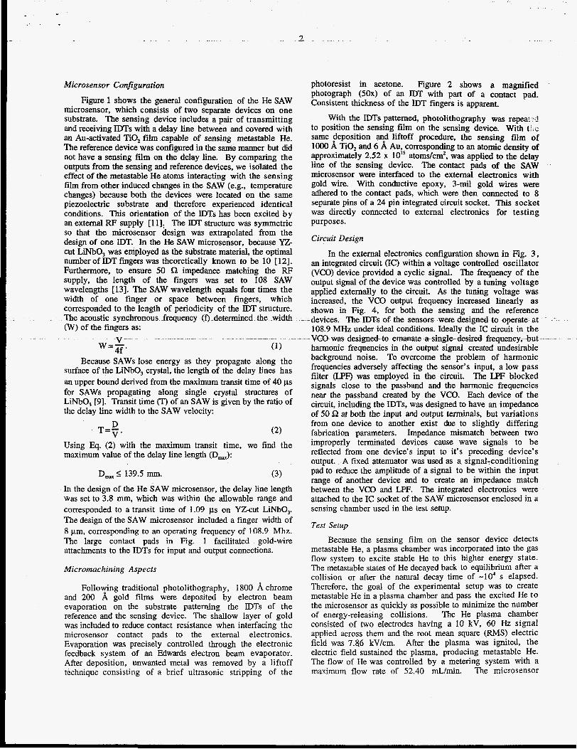
Following traditional photolithography, 1800 8, chrome and 200 8, gold films were deposited by electron beam evaporation on the substrate patterning the IDTs of the reference and the sensing device. The shallow layer of gold was included to reduce contact resistance when interfacing the microsensor contact pads to the external electronics. Evaporation was precisely controlled through the electronic feedback system of an Edwards electron beam evaporator. After deposition, unwanted metal was removed by a liftoff technique consisting of a brief ultrasonic stripping of the
photoresist in acetone. Figure 2 shows a magnified photograph (50x1 of an IDT with part of a contact pad. Consistent thickness of the IDT fingers is apparent.
With the IDTs patterned, photolithography was repeat .3 to position the sensing film on the sensing device. With t..c same deposition and liftoff procedure, the sensing Nm of lo00 8, T i 4 and 6 8, Au, corresponding to an atomic density of approximately 2.52 x 10’’ atoms/cm2, was applied to the delay line of the sensing device. The contact pads of the SAW microsensor were interfaced to the external electronics with gold wire. With conductive epoxy, 3-mil gold wires were adhered to the contact pads, which were then connected to 8 separate pins of a 24 pin integrated circuit socket. This socket was directly connected to external electronics for testing purposes.
Circuit Design
In the external electronics configuration shown in Fig. 3 , an integrated circuit (IC) within a voltage controlled oscillator (VCO) device provided a cyclic signal. The frequency of the output signal of the device was controlled by a tuning voltage applied externally to the circuit. As the tuning voltage was increased, the VCO output frequency increased linearly as shown in Fig. 4, for both the sensing and the reference devices. The IDTs of the sensors were designed to operate at 108.9 MHz under ideal conditions. Ideally the IC circuit in the VCO was designed-tu emanate zt-singledesired fteqtlency, but harmonic frequencies in the output signal created undesirable background noise. To overcome the problem of harmonic frequencies adversely affecting the sensor’s input, a low pass filter was employed in the circuit. The LPF blocked signals close to the passband and the harmonic frequencies near the passband created by the VCO. Each device of the circuit, including the IDTs, was designed to have an impedance of 50 a at both the input and output terminals, but variations from one device to another exist due to slightly differing fabrication parameters. Impedance mismatch between two improperly terminated devices cause wave signals to be reflected from one device’s input to it’s preceding device’s output. A fixed attenuator was used as a signal-conditioning pad to reduce the amplitude of a signal to be within the input range of another device and to create an impedance match between the VCO and LPF. The integrated electronics were attached to the IC socket of the SAW microsensor enclosed in a sensing chamber used in the test setup.
Test Setup
Because the sensing film on the sensor device detects metastable He, a plasma chamber was incorporated into the gas flow system to excite stable He to this higher energy state. The metastable states of He decayed back to equilibrium after a collision or after the natural decay time of -10‘ s elapsed. Therefore, the goal of the experimental setup was to create metastable He in a plasma chamber and pass the excited He to the microsensor as quickly as possible to minimize the number of energy-releasing collisions. The He plasma chamber consisted of two electrodes having a 10 kV, 60 Hz signal applied across them and the root mean square (RMS) electric field was 7.86 kV/cm. After the plasma was ignited, the electric field sustained the plasma, producing metastable He. The flow of He was controlled by a metering system with a maximum flow rate of 52.40 mllmin. The microsensor

3
chamber was 5 x 5 x 3 cm and allowed for an integrated circuit socket to be plugged into it.
Results
The present application of the SAW sensor for inert gas detection was enhanced by the one-to-one correspondence of metastable atoms exposed during surface interaction. The frequency-shift difference between the sensing and the reference devices was of prime importance in the present measurements.
Figure 5 shows experimental variation with time elapsed of the frequency shift, lfs-fJ, where f, is the sensor frequency and f, is the reference frequency. Figure 6 shows variation of If,-f,l with increasing He pressure. Because both the sensing and the reference devices experience identical environments, the frequency shifts were independent of most parameters although it is possible that there may be small variations in the sensing behavior sensor (because of dust trapped in the IDT fingers and nonunifonnity with respect to the spacing between the fingers in the IDT due to a possible change in processing conditions). These small changes were not noticeable when experiments were run in vacuum for a long period of time, thereby implying that the difference in frequency between the sensing and the reference devices was negligible to begin with, i.e., below the kHz level.
As can be observed ._ from ._ Fig. 5, at the onset of plasma discharge, when production of metasGble He atoms began, there was an initial steep rise in the frequency shift due to the activation of the Au atoms overlying the TiO, thin film. The metastable He collided with the sensing film, thereby imparting its decay energy to the film. With this additional energy, the Au impurities in the semiconducting TiO, film were activated as deep traps, varying the electrical conductivity of the film. Ultimately, this decay in electrical conductivity affected the SAW and was manifested as a frequency shift in the 4-12 kHz range in the output RF signal.
Due to saturation of the Au atoms, and therefore limiting the number of Au atoms available for interaction with the metastable He atoms, a constant variation was observed in the curve where increased pressure of He (seen in Fig. 6) did not increase the electrical conductivity of TiO,. The small abrupt changes in the curve may be due to interaction of highly energized metastable He atoms with Au atoms, stripping the Au atoms altogether from the surface of the sensing film. These stripped Au atoms would be removed instantly from the system due to continuous pumping of the sensing chamber. The momentary interaction of the metastable He atoms may also increase If,-f,l before the Au atoms are stripped and after stripping, lf,-f,l may decrease. When the plasma was shut off, no metastable He atoms were produced and, as expected, the change in the frequency shift If,-f,l decreased dramatically.
These results clearly demonstrate the role of metastable He atoms in the detection of surface interaction with other atoms, in this case Au.
CONCLUSIONS
This work is related to designing, fabricating and testing a surface acoustic wave (SAW) sensor to be used for detecting inert gases, particularly helium. The microsensor assembly consisted of two SAW configurations, one a reference with no
deposition at the delay line and the other sensing with an Au- activated Ti4 e-beam-deposited thin film (sensitive to electrical conductivity changes) on the delay line. The IDTs and delay lines were fabricated by photolithography techniqL -2 on a single Y-cut L M O j substrate oriented for Z propagation of SAWS.
The variation in electrical conductivity due to exposure to metastable He was translated as a frequency shift, shown to be in the 4-12 kHz range, in~the assembly. In the future, various characteristics of the SAW sensor, e.g., width of the delay line, temperature exposure, operating frequency, IDT finger width and separation, and separation between IDTs and delay line will be studied to better understand and optimize the variation of acoustic wave velocity and operating frequency of the SAW device. Different operating frequencies will be studied and several configurations of the number of IDT fingers, and finger widths will be employed.
A C K N O W L E ~ ~
The authors would like to acknowledge the funding granted to them by the U.S. Department of Energy and by the Argonne National Laboratory Directed Research and Development project, under Contract W-31-109-ENG-88. The authors would also like to thank Dr. James Bobis for his help in circuit d9sign.
131
[7
181
. REmmm. -
Lord Rayleigh, “On waves propagated along the plan surface of an elastic solid,” Proc. London Math. SOC.,
J. F. Vetelino, R. K. Lade and R. S . Falconer, “Hydrogen sulfide surface acoustic wave gas detector,” IEEE Transactions on Ultrasonics, Ferroelectrics, and Frequency Control, vol. UFFC-34, no. 2, pp. 156-161, 1987.
Y. V. Gulayev, “On the nonlinear theory of ultrasound amplification in semiconductors,” IEEE Transactions on Sonics and Ultrasonics, vol. SU-17, no. 2, pp. 11 1-122, 1970.
V. Chaplanov, V. Filippov and A. Terentjev, “Sensitivity of PdSi04Si sensor to humidity,” Sensors and Actuators B , vol. 5 , pp. 187-188, 1991.
R. Adler, “Simple theory of acoustic amplification,” IEEE Transactions on Sonics and Ultrasonics, vol. SU- 18, no. 3, pp. 115-118, 1971. L. Yu. Kupriyanov, V. I. Tsivenko, and I. A. Myasnikov, “Electronic Phenomena in the Interaction of Inert-Gas Metastable Atoms with Disperse Metal-Semiconductor Structures”, Zh. Fiz. Khim., vol. 58 (1984) pp. 1156- 1162. L. Y. Kupriyanov and V. I. Tsivenko, “Interaction of metastable inert gas atoms with the surface of titanium dioxide activated with gold,” Russian Journal of Physical Chemistry, vol. 61, no. 3, pp. 430-431, 1987.
J. W. Gardner, Microsensors Principles and Applications. New York: John Wiley & Sons, Inc.,
V O ~ . 17, pp. 4-11, 1885.
1994, pp.106-110.

4
[9] H. Wohltjen, "Mechanism of operation and design considerations for surface acoustic wave device vapour sensors," Sensors and actuators, vol. 5 , pp. 307-325, 1984.
[lo] J. Temmyo, I. Kotaka, T. inamura and S. Yoshikawa, "Precise measurement of SAW propagation velocity on LiNbO,," L!XE Transactions on Sonics and Ultrasonics, vol. SU-27, no. 4, pp. 218-219, 1980.
[ I l l R. M. White, P. J. Wicher, S. W. Wenzel and E. T. Zellers, "Plate-mode ultrasonic oscillator sensors," LEEE Transactions on Ultrasonics, Ferroelectrics, and Frequency Control, vol. UFFC-34, no. 2, pp. 162-171, 1987.
[12] D. P. Morgan, "Surface acoustic wave devices and applications," Ultrasonics, pp. 121-131, May 1973.
[13J R. W. White, "Surface elastic waves," Proceedings of the
Fig. 3: Electronic components assembly.
IEEE, V O ~ . 68, pp. 1238-1277, August 1970.
ToD View:
0 2 4 6 8 10 [?I Tuning Voltage, V
Fig. 4: Tuning voltage vs. the operating frequency. Sensing Film
Delay Line
Cross-sectional View:
2 t . 1 * I * v 8 1 I I I I t * * I 1 ' ;J
Plasma Time, min P k W O f 50 100 150 2aOT
On
Fig. 1: Top and cross-sectional views of SAW microsensor configuration.
Fig. 6: Elapsed time vs. frequency difference between sensor and reference devices. Also indicated are plasma onloff points.
x 10 e
$ 6 5
2 1 0 * ' I " ' I " ' I " ' I " ' I " ' 0 20 40 60 80 100 120
Helium Pressure,kPa
Fig. 7: He pressure vs. frequency difference between sensor and reference devices.
Fig. 2: Optical photomicrograph of a p o ~ i o n of SAW microsensor showing IDTs and part of contact pad (50x).