Embed Size (px)
Citation preview
University of Tennessee, Knoxville University of Tennessee, Knoxville
TRACE: Tennessee Research and Creative TRACE: Tennessee Research and Creative
Exchange Exchange
Masters Theses Graduate School
8-2012
A Memory Controller for FPGA Applications A Memory Controller for FPGA Applications
Bryan Jacob Hunter [email protected]
Follow this and additional works at: https://trace.tennessee.edu/utk_gradthes
Part of the Other Electrical and Computer Engineering Commons
Recommended Citation Recommended Citation Hunter, Bryan Jacob, "A Memory Controller for FPGA Applications. " Master's Thesis, University of Tennessee, 2012. https://trace.tennessee.edu/utk_gradthes/1305
This Thesis is brought to you for free and open access by the Graduate School at TRACE: Tennessee Research and Creative Exchange. It has been accepted for inclusion in Masters Theses by an authorized administrator of TRACE: Tennessee Research and Creative Exchange. For more information, please contact [email protected].
To the Graduate Council:
I am submitting herewith a thesis written by Bryan Jacob Hunter entitled "A Memory Controller
for FPGA Applications." I have examined the final electronic copy of this thesis for form and
content and recommend that it be accepted in partial fulfillment of the requirements for the
degree of Master of Science, with a major in Computer Engineering.
Gregory D. Peterson, Major Professor
We have read this thesis and recommend its acceptance:
Gregory D. Peterson, Hairong Qi, Nathanael Paul
Accepted for the Council:
Carolyn R. Hodges
Vice Provost and Dean of the Graduate School
(Original signatures are on file with official student records.)
To the Graduate Council:
I am submitting herewith a thesis written by Bryan Jacob Hunter entitled “A Memory
Controller for FPGA Applications.” I have examined the final paper copy of this
thesis for form and content and recommend that it be accepted in partial fulfillment
of the requirements for the degree of Master of Science, with a major in Computer
Engineering.
Dr. Gregory D. Peterson, Major
Professor
We have read this thesisand recommend its acceptance:
Dr. Hairong Qi
Dr. Nathanael Paul
Accepted for the Council:
Carolyn R. Hodges
Vice Provost and Dean of the Graduate School
To the Graduate Council:
I am submitting herewith a thesis written by Bryan Jacob Hunter entitled “A Memory
Controller for FPGA Applications.” I have examined the final electronic copy of this
thesis for form and content and recommend that it be accepted in partial fulfillment
of the requirements for the degree of Master of Science, with a major in Computer
Engineering.
Dr. Gregory D. Peterson, Major Professor
We have read this thesisand recommend its acceptance:
Dr. Hairong Qi
Dr. Nathanael Paul
Accepted for the Council:
Carolyn R. Hodges
Vice Provost and Dean of the Graduate School
(Original signatures are on file with official student records.)
A Memory Controller for FPGA
Applications
A Thesis Presented for
The Master of Science
Degree
The University of Tennessee, Knoxville
Bryan Jacob Hunter
August 2012

c© by Bryan Jacob Hunter, 2012
All Rights Reserved.
ii
Acknowledgements
I would like to thank everyone that has supported me through the years. I would
name you, but then this page might be longer than my thesis.
iii

Abstract
As designers and researchers strive to achieve higher performance, field-programmable
gate arrays (FPGAs) become an increasingly attractive solution. As coprocessors,
FPGAs can provide application specific acceleration that cannot be matched by
modern processors. Most of these applications will make use of large data sets,
so achieving acceleration will require a capable interface to this data. The research
in this thesis describes the design of a memory controller that is both efficient and
flexible for FPGA applications requiring floating point operations. In particular, the
benefits of certain design choices are explored, including: scalability, memory caching,
and configurable precision. Results are given to prove the controller’s effectiveness
and to compare various design trade-offs.
iv
Contents
List of Tables vii
List of Figures viii
1 Introduction and Motivation 1
2 Hardware Design 3
2.1 Platform . . . . . . . . . . . . . . . . . . . . . . . . . . . . . . . . . . 3
2.2 FPGA Design . . . . . . . . . . . . . . . . . . . . . . . . . . . . . . . 4
2.2.1 Top Level Module . . . . . . . . . . . . . . . . . . . . . . . . . 5
2.2.2 Memory Controller . . . . . . . . . . . . . . . . . . . . . . . . 7
2.2.3 User Design . . . . . . . . . . . . . . . . . . . . . . . . . . . . 16
3 Software Design 21
3.1 Software and FPGA Interface . . . . . . . . . . . . . . . . . . . . . . 21
3.2 Program Overview . . . . . . . . . . . . . . . . . . . . . . . . . . . . 23
4 Implementation and Results 25
4.1 Hardware Implementation and Performance Models . . . . . . . . . . 25
4.2 Software Implementation . . . . . . . . . . . . . . . . . . . . . . . . . 30
4.3 Overall Performance Model . . . . . . . . . . . . . . . . . . . . . . . 32
4.4 Expected Results . . . . . . . . . . . . . . . . . . . . . . . . . . . . . 32
4.5 Results . . . . . . . . . . . . . . . . . . . . . . . . . . . . . . . . . . . 38
v
5 Discussion 44
6 Conclusion 46
7 Related Work 47
Bibliography 54
Vita 59
vi

List of Tables
2.1 Specs for Altera’s Floating Point Megafunctions. . . . . . . . . . . . . 19
3.1 Functions from PROC API used in design. . . . . . . . . . . . . . . . 22
4.1 Number of floating-point units in design that can fit into the FPGA
with given precision. . . . . . . . . . . . . . . . . . . . . . . . . . . . 26
4.2 Fitter Summary provided by Quartus II Software. . . . . . . . . . . . 27
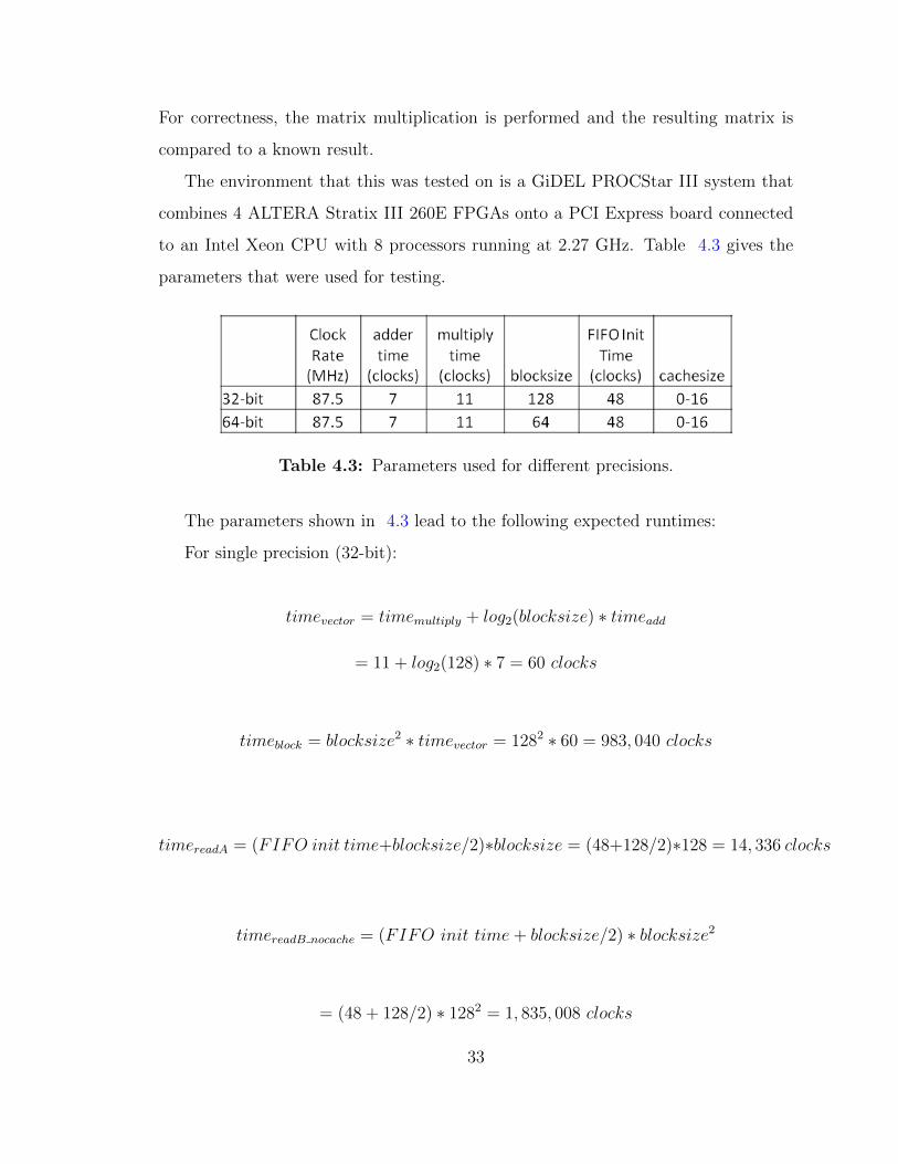
4.3 Parameters used for different precisions. . . . . . . . . . . . . . . . . 33
vii
List of Figures
2.1 PROCStar III Board. . . . . . . . . . . . . . . . . . . . . . . . . . . . 4
2.2 System Design Overview. . . . . . . . . . . . . . . . . . . . . . . . . . 5
2.3 Toggle signal that gives memory control to Hardware or Software. . . 6
2.4 Timing Diagram for PROCMultiport IP for Reading and Writing to
Memory [12]. . . . . . . . . . . . . . . . . . . . . . . . . . . . . . . . 8
2.5 Conversion Process to and from SDRAM. . . . . . . . . . . . . . . . 9
2.6 Conversion from Double Precision to 24 bit precision with exponent
width 6 and mantissa width 17. . . . . . . . . . . . . . . . . . . . . . 11
2.7 Conversion from 24 bit precision with exponent width 6 and mantissa
width 17 to Double Precision. . . . . . . . . . . . . . . . . . . . . . . 12
2.8 Conversion from 24 bit precision with exponent width 6 and mantissa
width 17 to Double Precision. . . . . . . . . . . . . . . . . . . . . . . 12
2.9 Iteration of matrix multiply. . . . . . . . . . . . . . . . . . . . . . . . 17
2.10 Hardware view of one iteration of matrix multiply. . . . . . . . . . . . 18
4.1 Matrix multiply divided into blocked matrix multiply and then vector
multiply. . . . . . . . . . . . . . . . . . . . . . . . . . . . . . . . . . . 28
4.2 Mean Squared Error vs Matrix Size for different precisions of matrix
multiplication. . . . . . . . . . . . . . . . . . . . . . . . . . . . . . . . 38
4.3 Execution Times vs Matrix Size for FPGA (using all 4 FPGAs) and
CPU implementations. . . . . . . . . . . . . . . . . . . . . . . . . . . 39
viii
4.4 Speedup of matrix multiplication on FPGA compared to double
precision matrix multiplication performed on CPU. . . . . . . . . . . 40
4.5 Execution Times vs Matrix Size for matrix multiplication on FPGA
with caching and no caching. . . . . . . . . . . . . . . . . . . . . . . . 40
4.6 Speedup of using caching compared to not using caching on FPGA. . 41
4.7 Scalability for single precision. . . . . . . . . . . . . . . . . . . . . . . 42
4.8 Speedup for single precision over using 1 FPGA. . . . . . . . . . . . . 42
4.9 Scalability for double precision. . . . . . . . . . . . . . . . . . . . . . 43
4.10 Speedup for double precision over using 1 FPGA. . . . . . . . . . . . 43
7.1 Authentication with Traditional Two-factor Hardware Security To-
kens. [30] . . . . . . . . . . . . . . . . . . . . . . . . . . . . . . . . . 49
7.2 Secure Identity Management through Hardware-enforced Security Poli-
cies. . . . . . . . . . . . . . . . . . . . . . . . . . . . . . . . . . . . . 50
7.3 Design of Prototype. . . . . . . . . . . . . . . . . . . . . . . . . . . . 53
ix
Chapter 1
Introduction and Motivation
A field-programmable gate array (FPGA) is an integrated circuit that consists of logic
blocks of digital circuitry that can be programmed as hardware. Rather than being
restricted to only certain hardware functions, as you are with application-specific
integrated circuits (ASICs), an FPGA can be programmed for specific functions and
applications [2]. As a result, FPGAs are targeted for acceleration for various problems.
As coprocessors, FPGAs have shown remarkable speedups for certain applications.
The main reasons for achieving these performance gains come from the deep pipelines
and parallel execution units that FPGAs have to offer [3]. In addition, on-the-
fly reconfiguration presents an oppurtunity to exploit multiple FPGA coprocessing
designs allowing for a wider range of target applications. However, many of these
applications will require external memory for the FPGA to access in order to solve
larger problems. Therefore, a smart memory interface is crucial in order to achieve
the potential performance benefits provided by FPGAs [14].
Generally, applications that require computational acceleration involve floating-
point calculations. For this reason, the memory controller was designed specifically
for reading and writing floating point values. An advantage of using floating-point
representation is the wide range of values that can be represented [16]. Conversely,
a number may not need as many bits to be represented accurately. For example,
1

assume a value can be represented accurately with 40 bits. On a normal processor,
this number would require using double precision (64-bit) representation and a double
precision floating-point unit. On the other hand, an FPGA can be programmed to
handle 40-bit floating-point numbers that use smaller registers and smaller floating-
point units. This results in extra space to allow for more concurrent units that
will increase parallelism and thus performance. In order to accomodate this feature,
the memory controller was designed to handle floating-point numbers with arbitrary
precisions up to 64 bits.
The research presented within this thesis discusses the design and implementation
of a memory controller for FPGA applications using floating-point numbers. The rest
of the content will be laid out as follows. First, the platform that enabled such research
is given. Second, the FPGA design will be presented with a particular emphasis on
the design choices that were made to achieve a robust and efficient controller. Next,
an overview of the software design will be given which will make the FPGA useful
as a coprocessor. Finally, results will be shown to prove the memory controller’s
effectiveness for some given implementations.
2
Chapter 2
Hardware Design
This chapter will describe the hardware design, including the actual FPGA design
and the development platform that makes all of this possible.
2.1 Platform
Before delving into the actual design, the platform that enables this idea of a
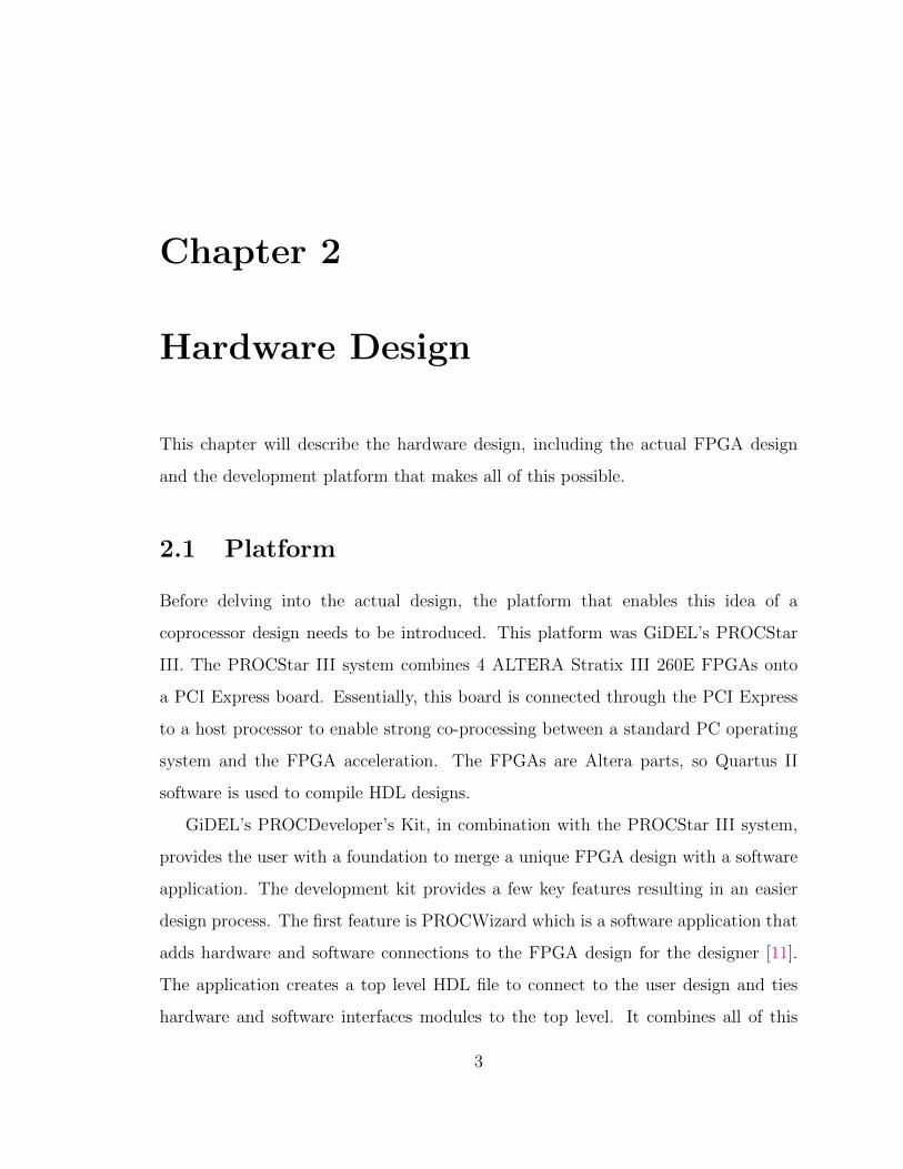
coprocessor design needs to be introduced. This platform was GiDEL’s PROCStar
III. The PROCStar III system combines 4 ALTERA Stratix III 260E FPGAs onto
a PCI Express board. Essentially, this board is connected through the PCI Express
to a host processor to enable strong co-processing between a standard PC operating
system and the FPGA acceleration. The FPGAs are Altera parts, so Quartus II
software is used to compile HDL designs.
GiDEL’s PROCDeveloper’s Kit, in combination with the PROCStar III system,
provides the user with a foundation to merge a unique FPGA design with a software
application. The development kit provides a few key features resulting in an easier
design process. The first feature is PROCWizard which is a software application that
adds hardware and software connections to the FPGA design for the designer [11].
The application creates a top level HDL file to connect to the user design and ties
hardware and software interfaces modules to the top level. It combines all of this
3
Figure 2.1: PROCStar III Board.
into a Quartus Project File to be compiled and generates a C++ Class Application
Driver to interface these modules from software. The second feature provided by
this development kit is the PROC Application Programming Interface (PROC API)
which provides a set of functions used to access the PROC boards [10]. This API uses
the application driver created by PROCWizard to communicate with the generated
HDL design via the PCI express bus. The API is also used to perform hardware
initializations, load FPGA designs, and set clock frequencies. The third feature that
was used was the PROCMultiport IP [12]. This feature allows rapid parallel access
to on-board SDRAM from the FPGA, as well as interfacing software to the SDRAM
to allow large memory transfers over the PCIe bus.
In essence, the features above give the PROCStar III system the abstraction of
being a coprocessor. The PROCStar III platform provides quick development, on-
the-fly reconfiguration, hardware and software co-design, and high performance IPs.
2.2 FPGA Design
This section will describe the entire FPGA design in a top-down approach. The
modules that will be described were written in VHDL and compiled using Quartus
II software.
4
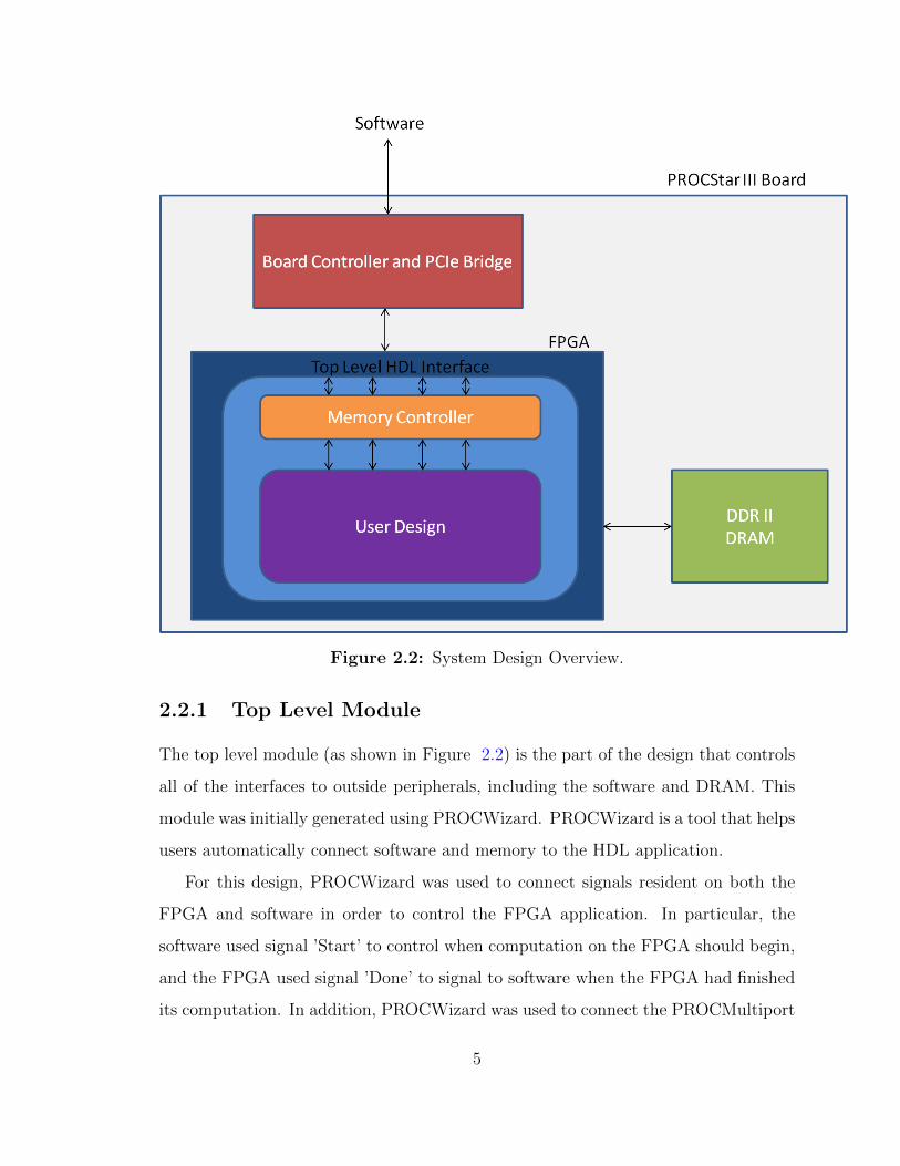
Figure 2.2: System Design Overview.
2.2.1 Top Level Module
The top level module (as shown in Figure 2.2) is the part of the design that controls
all of the interfaces to outside peripherals, including the software and DRAM. This
module was initially generated using PROCWizard. PROCWizard is a tool that helps
users automatically connect software and memory to the HDL application.
For this design, PROCWizard was used to connect signals resident on both the
FPGA and software in order to control the FPGA application. In particular, the
software used signal ’Start’ to control when computation on the FPGA should begin,
and the FPGA used signal ’Done’ to signal to software when the FPGA had finished
its computation. In addition, PROCWizard was used to connect the PROCMultiport
5
IP to the top level design. The PROCMultiport IP is an HDL design IP that connects
the FPGA to the SDRAM, as well as connecting the software through the FPGA to
the SDRAM. This IP allows for quick memory transfers from the host processor to
the SDRAM that will be accessible by the FPGA.
At this point, PROCWizard has created a module that will allow the software
to control the FPGA and send data to memory that can be accessed by the FPGA
application. These are the two essential functions that must be provided in order to
have a coprocessing enviroment. The signals that coordinate directly with software
are just that - signals. Therefore, these signals are easily tied into the user design.
On the contrary, correctly connecting into the FPGA memory, or the SDRAM, is
difficult to implement. The need for a memory controller is apparent.
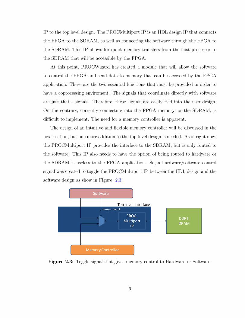
The design of an intuitive and flexible memory controller will be discussed in the
next section, but one more addition to the top-level design is needed. As of right now,
the PROCMultiport IP provides the interface to the SDRAM, but is only routed to
the software. This IP also needs to have the option of being routed to hardware or
the SDRAM is useless to the FPGA application. So, a hardware/software control
signal was created to toggle the PROCMultiport IP between the HDL design and the
software design as show in Figure 2.3.
Figure 2.3: Toggle signal that gives memory control to Hardware or Software.
6
2.2.2 Memory Controller
As stated above, GiDEL’s PROCMultiport IP is used as the top level interface to
memory. The PROCMultiport IP is a memory controller by itself, but it does not
provide certain features that are required to make the it useful for actual design. As
a result, an extension to this IP was designed to provide some key benefits. Four
main features went into the design of the memory controller: usability, flexibility,
scalability, and performance. The following sections will present the design of the
memory controller with respect to these features.
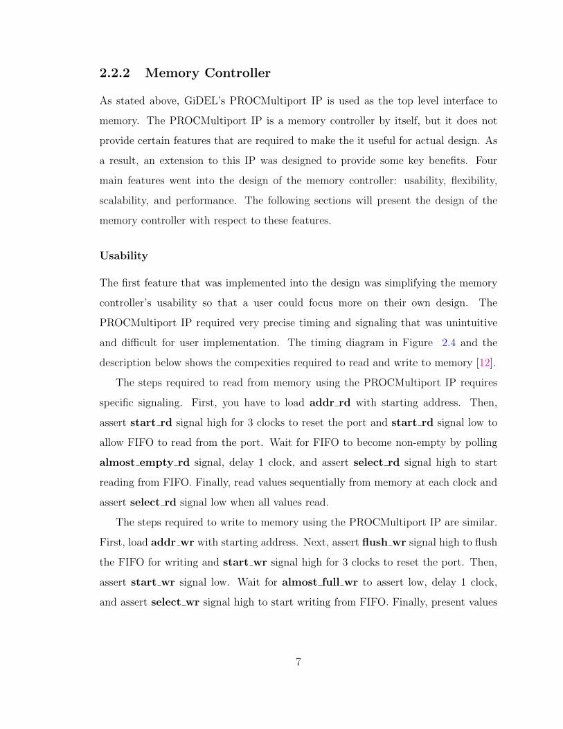
Usability
The first feature that was implemented into the design was simplifying the memory
controller’s usability so that a user could focus more on their own design. The
PROCMultiport IP required very precise timing and signaling that was unintuitive
and difficult for user implementation. The timing diagram in Figure 2.4 and the
description below shows the compexities required to read and write to memory [12].
The steps required to read from memory using the PROCMultiport IP requires
specific signaling. First, you have to load addr rd with starting address. Then,
assert start rd signal high for 3 clocks to reset the port and start rd signal low to
allow FIFO to read from the port. Wait for FIFO to become non-empty by polling
almost empty rd signal, delay 1 clock, and assert select rd signal high to start
reading from FIFO. Finally, read values sequentially from memory at each clock and
assert select rd signal low when all values read.
The steps required to write to memory using the PROCMultiport IP are similar.
First, load addr wr with starting address. Next, assert flush wr signal high to flush
the FIFO for writing and start wr signal high for 3 clocks to reset the port. Then,
assert start wr signal low. Wait for almost full wr to assert low, delay 1 clock,
and assert select wr signal high to start writing from FIFO. Finally, present values
7
Figure 2.4: Timing Diagram for PROCMultiport IP for Reading and Writing toMemory [12].
to write to memory at each clock and assert select wr signal low when all values
written.
Clearly, reading and writing to memory using PROCMultiport IP can quickly get
frustrating using all of these signals. This does not even mention the precise timing
constraints required to poll these signals and present data at the appropriate times.
Luckily, the memory controller that was designed will take care of all of this for you
and provide a much simpler interface.
The steps required to read and write memory using the Memory Controller begins
with asserting read or write high with addr set to the desired address. Then, wait
for data ready or write done to assert high. Finally, assert read or write low.
8
The usability of the above Memory Controller is far superior to the original. The
control is implemented by the controller itself and is not left up to the user. This
saves a lot of hassle and results in much quicker design times.
Flexibility
Perhaps the most useful attribute of the Memory Controller is its flexibility. It
supports configurable precision for floating point numbers. Allowing variable precision
gives the designer the oppurtunity to trade some accuracy for performance. For this
particular platform, the software interface enables designs with different precisions to
be loaded onto the FPGA on the fly. Designs can be coupled effectively to result in
both better performance and sufficient accuracy.
As stated earlier, the Memory Controller supports configurable precision, meaning
that the design has to be recompiled for different precisions. In order to change the
precision of the Memory Controller, only a few top level constants need to be changed:
PRECISION, MANTISSA, and EXPONENT. These are defined as constants inside
of a package list associated with the design.
Keeping the software design simple was a crucial aspect of the Memory Controller
design. As a result, the SDRAM was implemented to contain double precision values,
so that the software could make simple memory transfers. The Memory Controller
is what converts these double precision values down to the precision specified by the
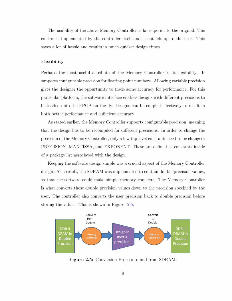
user. The controller also converts the user precision back to double precision before
storing the values. This is shown in Figure 2.5.
Figure 2.5: Conversion Process to and from SDRAM.
9
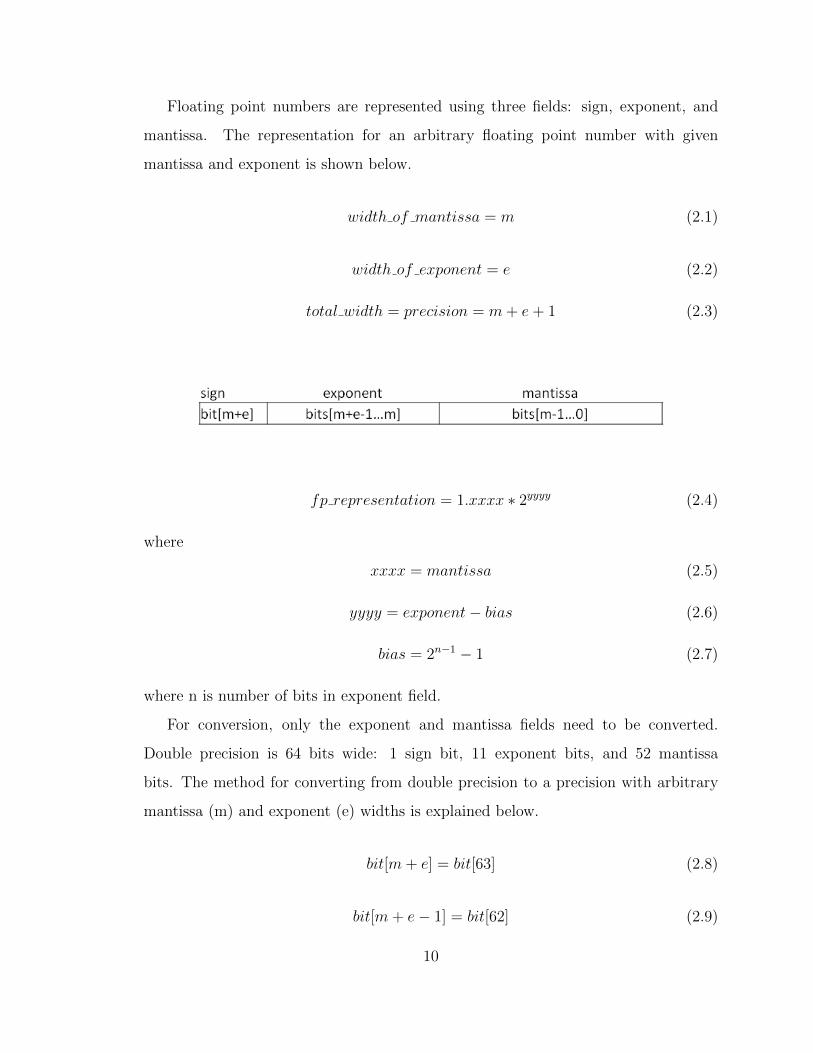
Floating point numbers are represented using three fields: sign, exponent, and
mantissa. The representation for an arbitrary floating point number with given
mantissa and exponent is shown below.
width of mantissa = m (2.1)
width of exponent = e (2.2)
total width = precision = m + e + 1 (2.3)
fp representation = 1.xxxx ∗ 2yyyy (2.4)
where
xxxx = mantissa (2.5)
yyyy = exponent− bias (2.6)
bias = 2n−1 − 1 (2.7)
where n is number of bits in exponent field.
For conversion, only the exponent and mantissa fields need to be converted.
Double precision is 64 bits wide: 1 sign bit, 11 exponent bits, and 52 mantissa
bits. The method for converting from double precision to a precision with arbitrary
mantissa (m) and exponent (e) widths is explained below.
bit[m + e] = bit[63] (2.8)
bit[m + e− 1] = bit[62] (2.9)
10
bits[m + e− 2...m] = bits[50 + e...52] (2.10)
bits[m− 1...0] = bits[51...52 −m] (2.11)
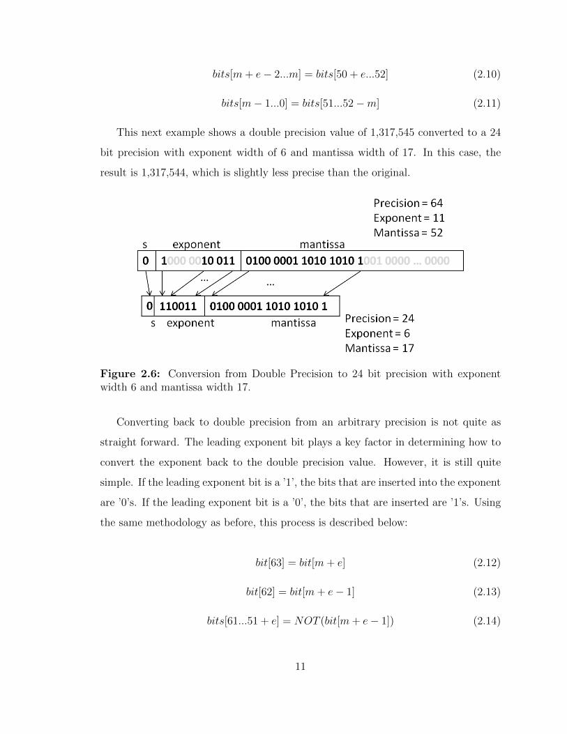
This next example shows a double precision value of 1,317,545 converted to a 24
bit precision with exponent width of 6 and mantissa width of 17. In this case, the
result is 1,317,544, which is slightly less precise than the original.
Figure 2.6: Conversion from Double Precision to 24 bit precision with exponentwidth 6 and mantissa width 17.
Converting back to double precision from an arbitrary precision is not quite as
straight forward. The leading exponent bit plays a key factor in determining how to
convert the exponent back to the double precision value. However, it is still quite
simple. If the leading exponent bit is a ’1’, the bits that are inserted into the exponent
are ’0’s. If the leading exponent bit is a ’0’, the bits that are inserted are ’1’s. Using
the same methodology as before, this process is described below:
bit[63] = bit[m + e] (2.12)
bit[62] = bit[m + e− 1] (2.13)
bits[61...51 + e] = NOT (bit[m + e− 1]) (2.14)
11

bits[50 + e...52] = bits[m + e− 2...m] (2.15)
bits[51...52 −m] = bits[m− 1...0] (2.16)
bits[51 −m...0] =′ 0′ (2.17)
Figure 2.7 shows the conversion when the leading exponent bit is a ’1’.
Figure 2.7: Conversion from 24 bit precision with exponent width 6 and mantissawidth 17 to Double Precision.
Figure 2.8 shows the conversion when the leading exponent bit is a ’0’.
Figure 2.8: Conversion from 24 bit precision with exponent width 6 and mantissawidth 17 to Double Precision.
The simple proof to show that the exponent conversion is correct is to show the
values of the exponent (2.6) in the floating point representation equation (2.4):
fp representation = 1.xxxx ∗ 2yyyy
yyyy = exponent− bias
12

Case 1 based on figure 2.7:
24-bit precision
bias = 2n−1 − 1 = 26−1 − 1 = 31
exponent = 51
yyyy = exponent− bias = 51 − 31 = 20
Double precision
bias = 2n−1 − 1 = 211−1 − 1 = 1023
exponent = 1043
yyyy = exponent− bias = 1043 − 1023 = 20
Case 2 based on figure 2.8:
24-bit precision
bias = 2n−1 − 1 = 26−1 − 1 = 31
exponent = 19
yyyy = exponent− bias = 19 − 31 = −12
Double precision
bias = 2n−1 − 1 = 211−1 − 1 = 1023
exponent = 1011
yyyy = exponent− bias = 1011 − 1023 = −12
Note: It is left up to the user to determine if the precision, mantissa, and exponent
are wide enough to satisfy a desired accuracy!
13
Performance
The most important aspect taken into account when designing the Memory Controller
was performance. If the Memory Controller is poorly designed, the overall acceleration
of the application will be limited. Two key aspects attributed to achieving better
performance: larger memory transfers and data reuse.
The reason that large memory transfers are needed is because there is a required
setup time to access the SDRAM. The PROCMultiport IP uses FIFO buffers to
shuttle data to and from memory to make connection and timing easier. When using
these FIFOs, enough data must fill up the FIFO before it can begin transferring
data to and from memory. As a result, every memory transaction incurs this delay
penalty to partially fill up the FIFO. Using larger memory transfers instead of smaller
transfers helps negate this delay factor. An example details this below.
The board used was a ProcStar III Board which defines the FIFO Depth as 256
words, so the delay required to fill up the FIFO before a memory transfer is:
delay = 16 + (FIFO depth ∗ 1/8) clocks (2.18)
delay = 16 + (256 ∗ 1/8) clocks (2.19)
delay = 48 clocks (2.20)
To show the difference between larger and smaller memory transfers, the read of a
128x128 matrix for different size transfers is explored. Assume a small transfer is 32
words and a large transfer is 1024 words. After the initial delay, one word per clock
is presented at the end of the FIFO.
Small Transfer (32 word blocks)
# of reads = 128 ∗ 128 = 16384
# of transfers = # of reads/32 = 512
14
total delay penalty = # of transfers ∗ delay = 512 ∗ 48 = 24576 clocks
total read time = total delay penalty + # of reads = 24576 + 16384 = 40960 clocks
Large Transfer (1024 word blocks)
# of reads = 128 ∗ 128 = 16384
# of transfers = # of reads/1024 = 16
total delay penalty = # of transfers ∗ delay = 16 ∗ 48 = 768 clocks
total read time = total delay penalty + # of reads = 768 + 16384 = 17152 clocks
As shown above, the bottleneck for small memory transfers quickly becomes the
delay penalty. For larger transfers, the delay penalty is almost completely negated.
speedup = 40960/17152 = 2.39
In order to take advantage of this aspect for different designs, the size of the
memory transfer is configurable. A memory transfer can be viewed as reading in
a very large cache line. The top level package list has a configurable parameter
LINE SIZE which dictates the size of the memory transfer. Based on the size and
requirements of the design, this parameter can be as large as it needs to be to achieve
better performance.
The second method for achieving better performance from the memory controller is
memory caching for data reuse. For applications that require data reuse, caching can
significantly increase performance. FPGAs also have the benefit that the cache can
be manually controlled for optimal usage. The performance improvement provided by
caching will vary based on the application, but caching will always be useful. The user
design section and results will cover the benefits provided by caching. This section
merely shows how it works.
15
The cache is set up based on the memory transfer size (or LINE SIZE) that was
discussed earlier. Without caching, every memory reference will read the data from
SDRAM resulting in a 48 clock delay time and 1 clock per word that is read. With
caching, this same penalty occurs for the first time a line of data is read. However,
when this line is read, the address (or tag) is stored. When a consecutive memory
reference to the same location is made, a cache hit is generated and the data is
immediately ready for use avoiding the cost to read it from the SDRAM again. The
parameter LINE SIZE determines how big the cache line is and the size of the tag.
Therefore, each memory reference checks the tag associated with it and determines
whether there is a hit or a miss. Cache misses read in LINE SIZE words from the
SDRAM and stores the upper part of the address in the tag field. The cache initially
starts out invalid to avoid the situation where the tag is equal to the address being
read at the start.
2.2.3 User Design
The user design is the main piece of the design that dictates how the memory
controller should be customized and used. Based on the application, certain design
choices can be made to improve performance. The user design that was used in this
research was matrix multiplication. This design was used in order to show both the
memory controller’s correctness and effectiveness. First, the overview of the design
will be given. Second, the design will be used to introduce how to interface the
memory controller in general. Finally, the customizations to the memory controller
based on the design will be shown.
Recall that matrix multiplication is:
C = A ∗B (2.21)
The data used for the matrix multiplication is controlled by software, so it can
easily be manipulated and transferred intelligently to the FPGA by the software
16
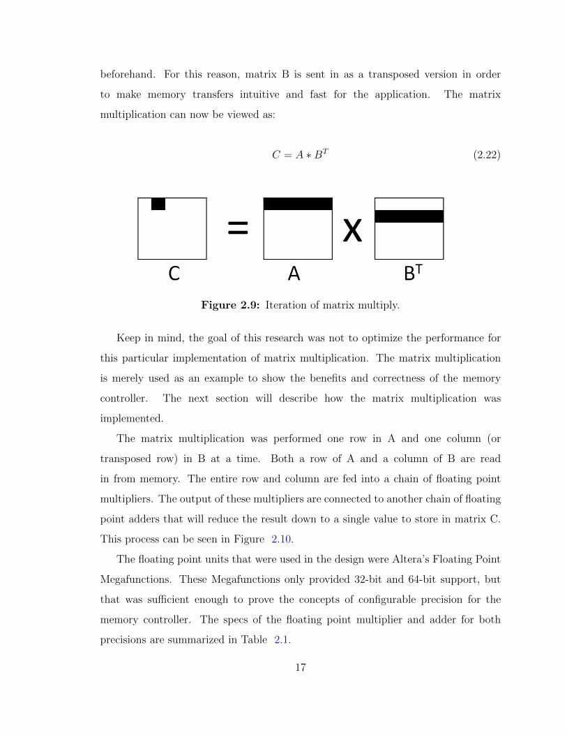
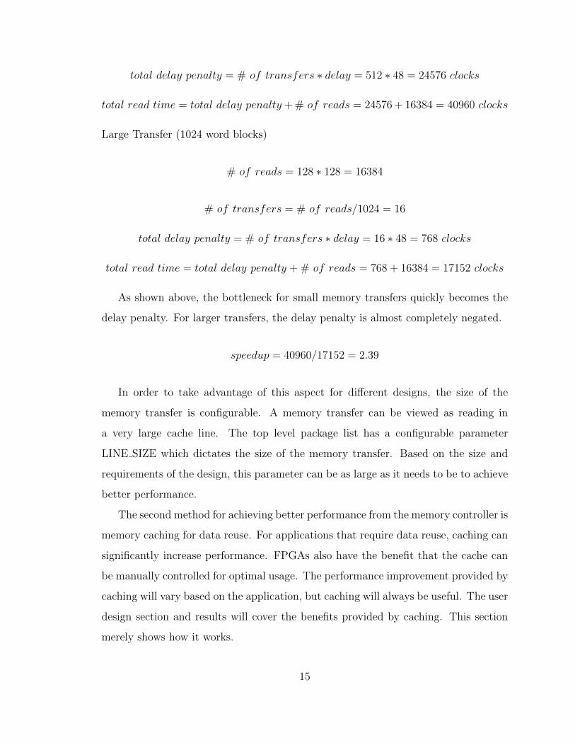
beforehand. For this reason, matrix B is sent in as a transposed version in order
to make memory transfers intuitive and fast for the application. The matrix
multiplication can now be viewed as:
C = A ∗BT (2.22)
Figure 2.9: Iteration of matrix multiply.
Keep in mind, the goal of this research was not to optimize the performance for
this particular implementation of matrix multiplication. The matrix multiplication
is merely used as an example to show the benefits and correctness of the memory
controller. The next section will describe how the matrix multiplication was
implemented.
The matrix multiplication was performed one row in A and one column (or
transposed row) in B at a time. Both a row of A and a column of B are read
in from memory. The entire row and column are fed into a chain of floating point
multipliers. The output of these multipliers are connected to another chain of floating
point adders that will reduce the result down to a single value to store in matrix C.
This process can be seen in Figure 2.10.
The floating point units that were used in the design were Altera’s Floating Point
Megafunctions. These Megafunctions only provided 32-bit and 64-bit support, but
that was sufficient enough to prove the concepts of configurable precision for the
memory controller. The specs of the floating point multiplier and adder for both
precisions are summarized in Table 2.1.
17
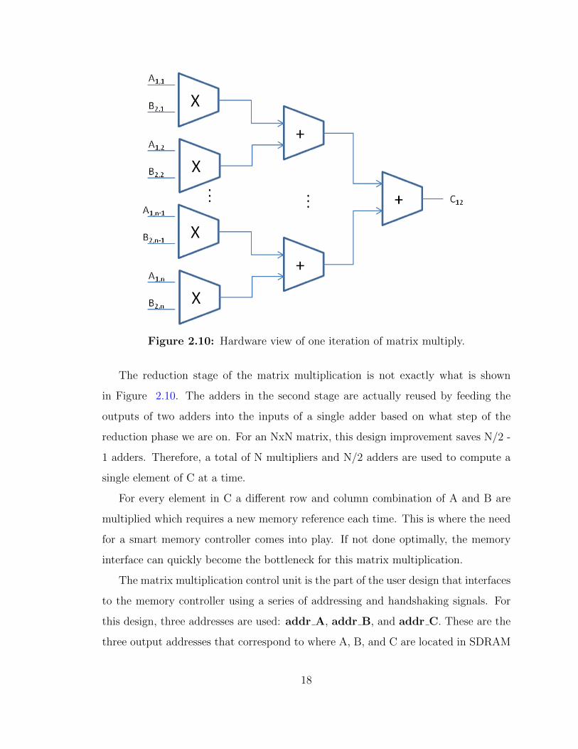
Figure 2.10: Hardware view of one iteration of matrix multiply.
The reduction stage of the matrix multiplication is not exactly what is shown
in Figure 2.10. The adders in the second stage are actually reused by feeding the
outputs of two adders into the inputs of a single adder based on what step of the
reduction phase we are on. For an NxN matrix, this design improvement saves N/2 -
1 adders. Therefore, a total of N multipliers and N/2 adders are used to compute a
single element of C at a time.
For every element in C a different row and column combination of A and B are
multiplied which requires a new memory reference each time. This is where the need
for a smart memory controller comes into play. If not done optimally, the memory
interface can quickly become the bottleneck for this matrix multiplication.
The matrix multiplication control unit is the part of the user design that interfaces
to the memory controller using a series of addressing and handshaking signals. For
this design, three addresses are used: addr A, addr B, and addr C. These are the
three output addresses that correspond to where A, B, and C are located in SDRAM
18
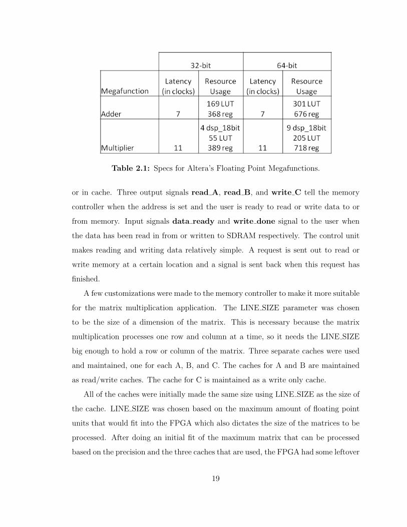
Table 2.1: Specs for Altera’s Floating Point Megafunctions.
or in cache. Three output signals read A, read B, and write C tell the memory
controller when the address is set and the user is ready to read or write data to or
from memory. Input signals data ready and write done signal to the user when
the data has been read in from or written to SDRAM respectively. The control unit
makes reading and writing data relatively simple. A request is sent out to read or
write memory at a certain location and a signal is sent back when this request has
finished.
A few customizations were made to the memory controller to make it more suitable
for the matrix multiplication application. The LINE SIZE parameter was chosen
to be the size of a dimension of the matrix. This is necessary because the matrix
multiplication processes one row and column at a time, so it needs the LINE SIZE
big enough to hold a row or column of the matrix. Three separate caches were used
and maintained, one for each A, B, and C. The caches for A and B are maintained
as read/write caches. The cache for C is maintained as a write only cache.
All of the caches were initially made the same size using LINE SIZE as the size of
the cache. LINE SIZE was chosen based on the maximum amount of floating point
units that would fit into the FPGA which also dictates the size of the matrices to be
processed. After doing an initial fit of the maximum matrix that can be processed
based on the precision and the three caches that are used, the FPGA had some leftover
19

space. Rather than wasting the space, the space was used to increase the cache size of
matrix B. The reason matrix B’s cache was chosen to be enlarged was because matrix
B is strided through more frequently than A or C. The nature of matrix multiply
already creates a solid foundation of cache hits for both A and C. Therefore, the
cache for matrix B is targeted to achieve a better performance improvement. The
size of the cache for B should be the largest multiple of 2 that will fit into the design.
This parameter is called CACHE SIZE in the top level package list.
20
Chapter 3
Software Design
The ability of FPGAs to be coprocessors relies heavily on the software design. For
large problem sizes, many FPGAs will need to be used and scaled together. The
management and coordination of these FPGAs must be maintained through software.
The following chapter will describe the development of the software design and how
it interfaces with the FPGA to achieve an efficient and scalable design.
3.1 Software and FPGA Interface
As stated in previous sections, GiDEL’s PROCDeveloper’s Kit provides the software
tools PROCWizard and PROC API. The PROCWizard tool creates the C++ class
application driver. PROC API provides a set of functions to access the PROC board
and to use the objects created by the application driver.
The C++ class application driver is essentially a header file that provides an
object for every variable on the FPGA that needs to have an interface to software.
The driver allocates a location in memory that is tied to the FPGA design through
the PCIe to communicate through variables. When an object is changed in software,
this change also takes place on the FPGA.
The objects that were used as directly shared variables were START, DONE, and
HW SW CONTROL. The other objects were referenced using the PROC API for
21

simplicity and will be described later. The object, START, was used as input to the
FPGA to signal when to begin processing. DONE was connected as output from the
FPGA to signal to the software when it was done processing. HW SW CONTROL
was used as input to the FPGA to give control to either the FPGA or software for
memory transactions. Clearly, each of these signals are easy to manipulate and only
require a 1 or 0 to coordinate the software with the FPGA.
The more difficult part is preparing the FPGA so that it is equipped with
everything that it needs to begin processing. This is where the PROC API is used.
Many other objects were created by PROCWizard for the application driver. These
objects are meant to be used by the functions provided by the API and not directly
manipulated like the signals above. The functions used for the design are described
in Table 3.1.
Table 3.1: Functions from PROC API used in design.
The functions above are very helpful. The LoadIC function allows for designs to
be loaded onto an FPGA on the fly on a specific FPGA. The DMA functions enable
the software to quickly and easily send large chunks of data to the FPGA or read
large chunks out. With the interface mechanism described above, the FPGA now has
the capability to function as a coprocessor.
22

3.2 Program Overview
This section will describe the software program that was written to control the matrix
multiplication performed by the FPGAs. The program is built around the application
driver described above. Essentially, the program will configure and initialize the
FPGA, perform the matrix multiplication, obtain the results, and compare the results
to a known solution.
The FPGA can only handle a maximum size matrix. However, from the software
side, a blocked version of matrix multiply can be implemented to multiply any size
matrices by using the FPGA multiple times. The following is a summary of the steps
required to carry out a matrix multiplication on one FPGA from the software side. A
more detailed implementation is described later which includes using multiple FPGAs
and certain design choices to enhance performance.
1. Initialize C++ class driver which loads the FPGA with the design using LoadIC
and ties it to software.
2. Allocate and initialize matrices A, B, and C on the host processor with random
values.
3. Create read and write buffers between host and PROC board using Creat-
eDMABuffer.
4. Fill write buffer with blocks of matrices A, B, and C (a block being the size of
matrix that the FPGA is configured to multiply).
5. Send buffer to PROC board DRAM using RunDMA on the write buffer.
6. Wait for transfer to complete using WaitDMADone.
7. Signal memory control to the FPGA by changing the signal HW SW CONTROL
to a 1.
8. Signal the FPGA to begin matrix multiply by changing START to a 1.
23

9. Wait for FPGA to change signal DONE to a 1.
10. Signal memory control to the host by changing the signal HW SW CONTROL
back to a 0.
11. Read buffer from PROC board DRAM using RunDMA on the read buffer.
12. Wait for transfer to complete using WaitDMADone.
13. Accumulate new C matrix with current C matrix on host.
14. Reset START signal to 0 which resets DONE signal on the FPGA so another
iteration can be performed.
15. Repeat steps 4-14 as needed until the entire matrix has been iterated through
and multiplied.
16. Check resulting matrix C against a software computed known solution.
17. Free buffers and memory.
The program described above allows the execution of any size of matrix
multiplication. It can be easily manipulated to work for functions other than matrix
multiplication. The foundation of the program is to be able to configure the FPGA,
perform the desired function by communicating with the FPGA, transfer data back
and forth, and observe the results.
24
Chapter 4
Implementation and Results
The following chapter will present the implementations used to test and validate the
memory controller. In particular, certain design choices will be compared against each
other and the results will be shown. The implementation is based on the user design
which is matrix multiplication. Design choices will vary based on the user design,
but the implementations used for matrix multiplication should be easy to modfiy or
extend for different designs.
4.1 Hardware Implementation and Performance
Models
The hardware design choices that were made for the memory controller were based on
two key factors: precision and area. These two factors happen to directly affect each
other. As stated in Chapter 2 in the User Design section, N floating-point multipliers
and N/2 floating-point adders are used for the design. The goal is to choose the
highest value of N that is a power of 2 that will fit into the design. The FPGA
area factor comes into play determining this N value. However, the precision of the
floating-point units determines the size of the units, so the precision also comes into
play. Consequently, the overall goal is now to minimize the precision to a desired
25
accuracy and maximize the N parameter. Once these values have been optimized,
the remaining space should be used to maximize the cache size. As a result, the
FPGA should be almost fully utilized and perform better.
Altera provides megafunctions for single (32-bit) and double (64-bit) precision,
but they do not provide configurable precision floating-point units for arbitrary
precisions. Therefore, the two implementations that were used for testing were single
and double precision. Even so, single and double precision floating-point units provide
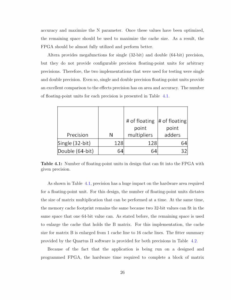
an excellent comparison to the effects precision has on area and accuracy. The number
of floating-point units for each precision is presented in Table 4.1.
Table 4.1: Number of floating-point units in design that can fit into the FPGA withgiven precision.
As shown in Table 4.1, precision has a huge impact on the hardware area required
for a floating-point unit. For this design, the number of floating-point units dictates
the size of matrix multiplication that can be performed at a time. At the same time,
the memory cache footprint remains the same because two 32-bit values can fit in the
same space that one 64-bit value can. As stated before, the remaining space is used
to enlarge the cache that holds the B matrix. For this implementation, the cache
size for matrix B is enlarged from 1 cache line to 16 cache lines. The fitter summary
provided by the Quartus II software is provided for both precisions in Table 4.2.
Because of the fact that the application is being run on a designed and
programmed FPGA, the hardware time required to complete a block of matrix
26

Table 4.2: Fitter Summary provided by Quartus II Software.
multiply can be directly calculated in clock cycles. The runtime consists of two
primary components: calculation time and memory time. Calculation time is less
variable and much easier to compute, so it will be looked at first. However, the
purpose of this research is tied to the memory portion, so many improvements can be
made to the calculation time. The calculation time is merely discussed for reference
and to be thorough.
The multiplication time is technically broken up into subsections as shown in
Figure 4.1. The overall matrix is divided into smaller blocks that are multiplied
together. Inside of these blocks, each row is multiplied by each column as a vector
multiply. Distinguishing these parts makes describing the model for runtime easier
to understand.
The following variables will be used in the runtime models:
N = square matrix size
blocksize = size of block from original matrix
timeadd = number of clocks to complete a floating point add
timemultiply = number of clocks to complete a floating point multiply
27
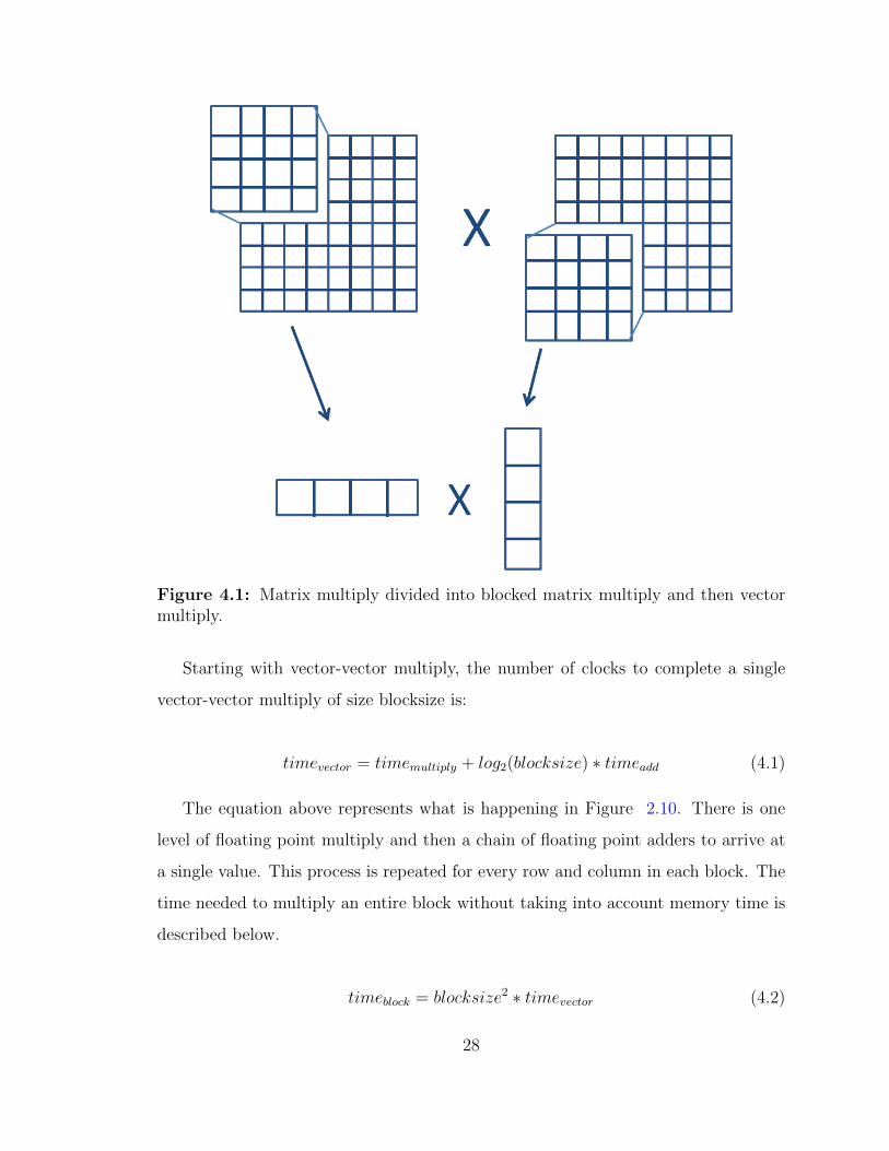
Figure 4.1: Matrix multiply divided into blocked matrix multiply and then vectormultiply.
Starting with vector-vector multiply, the number of clocks to complete a single
vector-vector multiply of size blocksize is:
timevector = timemultiply + log2(blocksize) ∗ timeadd (4.1)
The equation above represents what is happening in Figure 2.10. There is one
level of floating point multiply and then a chain of floating point adders to arrive at
a single value. This process is repeated for every row and column in each block. The
time needed to multiply an entire block without taking into account memory time is
described below.
timeblock = blocksize2 ∗ timevector (4.2)
28
The memory time required to perform this blocked matrix multiply is a bit more
complicated. There are two memory transfers to consider: the time to transfer data
across the PCIe bus to and from the PROCBoard and the time spent reading and
writing memory using the FPGA. Transferring data across the PCIe bus is difficult
to model because it depends on the system that the platform is running on, so this
memory time will be referred to as overhead. The FPGA memory transfers can be
modeled in three parts for this application: reading the A matrix, reading the B
matrix, and writing the C matrix. The number of clocks used by the FPGA for
memory operations for one block of the matrix multiply defined below.
timereadA = (FIFO init time + blocksize/2) ∗ blocksize (4.3)
Inside of the parentheses is the amount of clocks required to read an entire row
of A. The FIFO init time is the setup time required to initialize the FIFO and read
from SDRAM. This time is required for every set of memory reads and writes. The
memory controller reads and writes two values to SDRAM per clock, so the blocksize
term inside of the parentheses is divided by 2. The other blocksize term is the number
of rows in A that need to be read. Each row of A is reused blocksize times before
having to move to the next row, so the memory does not need to be referenced as
frequently as the B matrix.
timereadB nocache = (FIFO init time + blocksize/2) ∗ blocksize2 (4.4)
Reading the B matrix from memory occurs more frequently. For each row of A,
every column of B has to be referenced, hence the extra blocksize term. When there
is enough room for caching part of the B matrix, part of the B matrix only needs to
be read once. Therefore, the time reduces to:
timereadB cache = (FIFO init time+blocksize/2)∗ (blocksize−cachesize)∗blocksize
29
+ (FIFO init time + cachesize ∗ blocksize/2) (4.5)
If the application operates on a smaller matrix and has enough hardware to cache
the entire matrix, the time becomes:
timeread fullcache = FIFO init time + (blocksize/2) ∗ blocksize (4.6)
The resulting matrix has the same timing model as reading the A matrix, but for
a different reason. A row of the C matrix is computed one element at a time. When
a full row is computed, the entire row is written back to SDRAM. Therefore, the
equation remains:
timewriteC = (FIFO init time + blocksize/2) ∗ blocksize (4.7)
Combining all of the factors from above, the required memory time to perform a
single block of a blocked matrix multiply is
timememory = timereadA + timereadB + timewriteC + overhead (4.8)
where overhead is the memory time required to transfer memory from software as
stated before.
4.2 Software Implementation
In order to make the hardware design useful, the FPGA must be controlled by
software as described in Chapter 3. This section describes how the software should
be implemented based on the platform used in order to achieve a more efficient and
scalable design.
A given platform will have a certain number of FPGAs, X, connected to it through
the PCIe bus. The goal is to achieve a parallelism of X based on the number
of FPGAs. This would require completely overlapping the software portion with
30

the hardware portion. This is not possible, but can be approached using two key
optimizations: overlapping software control and reduction with FPGA computation
and threading FPGA control between processors.
Overlapping software with FPGA computation is quite simple. For a blocked
matrix multiply, each FPGA is given blocks of the matrices to multiply. The results
are read back and have to be reduced into a single matrix before moving on to the next
iteration. In addition, the buffer to transfer the next iteration’s data has to be filled
with new blocks. This process and the reduction can be overlapped by performing
them while the next iteration is run on the FPGA using a simple three step process:
1. Send data to the FPGAs and begin FPGA computation. 2. Fill buffer with
next iteration’s data and reduce last iteration’s result. 3. Wait for FPGAs to finish
computation and read data from FPGAs. As a result, step 2 is completely overlapped
by the computation on the FPGAs.
Another way to increase the performance of the software design is to assign
seperate threads to control different FPGAs. Doing this allows each thread to
control its own data transfer between the CPU and FPGA and communicate with
its FPGA. This eliminates a single thread having to sequentially transfer data and
control communications between each FPGA which would slow down each iteration
because of blocking calls. Ideally, there will be one processor per FPGA. If there is
not, threading will still be benefitial because threads will context switch on longer
blocking calls.
The software implementation can be optimized to partially overlap with the FPGA
computation. Therefore, the software performance will be viewed as a constant term,
overheadsoftware. Overheadsoftware occurs for every iteration of the blocked matrix
multiply, so it becomes a significant term. Another term that is needed, but mitigated
when larger matrix computations are performed, is the initialization time required to
load the FPGAs and initialize the matrices. This term is very small in comparison
to the rest of the computation, especially on larger matrices, but will be included as
timeinitialize.
31
4.3 Overall Performance Model
The models for both the software and hardware can be combined to obtain the overall
performance model for a single matrix multiplication on a single FPGA. The first term
will be the initialization time required by software and only occurs once. The next
term is a combination of the software and hardware terms for each iteration of blocked
matrix multiply. These terms will have to be iterated through as outlined below:
timeoverall per block = (timememory + timeblock + overheadsoftware) (4.9)
timeoverall = (timeoverall per block) ∗ (N/blocksize)3 + timeinitialize (4.10)
The equation above is mostly predicated on the blocksize that is chosen. A smaller
blocksize will result in a much larger term to be cubed. However, it can also result in a
smaller timeoverall per block. For larger matrices, though, the goal is to fit the maximum
blocksize matrix multiplication in order to achieve the best performance.
When multiple FPGAs are used, the models change slightly. When there is at least
one processor for each FPGA, the parallelism nearly equals the number of FPGAs
and approaches the equation below:
timeoverall parallel = timeoverall/(# of FPGAs) (4.11)
4.4 Expected Results
Numerous tests were performed to validate the memory controller for correctness and
performance. Performance will be compared against various sizes of cache, single and
double precision, different levels of software optimization, and the number of FPGAs.
32
For correctness, the matrix multiplication is performed and the resulting matrix is
compared to a known result.
The environment that this was tested on is a GiDEL PROCStar III system that
combines 4 ALTERA Stratix III 260E FPGAs onto a PCI Express board connected
to an Intel Xeon CPU with 8 processors running at 2.27 GHz. Table 4.3 gives the
parameters that were used for testing.
Table 4.3: Parameters used for different precisions.
The parameters shown in 4.3 lead to the following expected runtimes:
For single precision (32-bit):
timevector = timemultiply + log2(blocksize) ∗ timeadd
= 11 + log2(128) ∗ 7 = 60 clocks
timeblock = blocksize2 ∗ timevector = 1282 ∗ 60 = 983, 040 clocks
timereadA = (FIFO init time+blocksize/2)∗blocksize = (48+128/2)∗128 = 14, 336 clocks
timereadB nocache = (FIFO init time + blocksize/2) ∗ blocksize2
= (48 + 128/2) ∗ 1282 = 1, 835, 008 clocks
33

timereadB cache = (FIFO init time+blocksize/2)∗ (blocksize−cachesize)∗blocksize
+(FIFO init time + cachesize ∗ blocksize/2)
timereadB cache = (48+128/2)∗ (128−16)∗128+(48+16∗128/2) = 1, 606, 704 clocks
timeread fullcache = FIFO init time+(blocksize/2)∗blocksize = 48+(128/2)∗128 = 8240 clocks
timewriteC = (FIFO init time+blocksize/2)∗blocksize = (48+128/2)∗128 = 14, 336 clocks
timememory = timereadA + timereadB + timewriteC + overhead = 1, 635, 376 + overhead
timeoverall per block = (timememory + timeblock) clocks + overheadsoftware
timeoverall per block = (1, 635, 376 + 983, 040) clocks + overheadsoftware
timeoverall per block (in sec) = 2, 618, 416/87, 500, 000Hz
34

= 0.0299 + overheadsoftware seconds
Therefore, the overall time to compute the product of two 1024 by 1024 matrices
on the FPGA becomes:
timeoverall = (N/blocksize)3 ∗ timeoverall per block + timeinitialize
= (1024/128)3 ∗ (0.0299 + overheadsoftware) + timeinitialize
= 512 ∗ (0.0299 + overheadsoftware) + timeinitialize
= 15.3088 + 512 ∗ overheadsoftware + timeinitialize seconds
The timeinitialize becomes a negligible term, but the overheadsoftware is still quite
noticeable. The overheadsoftware is small when using a single FPGA, but it is
introduced everytime a new block is needed to be loaded onto the FPGA. This term
does not increase linearly with the number of FPGAs, because much of the time
gets overlapped with itself and computation. This makes it hard to model the actual
overheadsoftware for different instances, but after many tests, the overhead for this
particular hardware will be modeled as approximately 0.002 seconds per block. The
calculation time is not much larger, so this becomes a significant term. The equations
now become:
overheadsoftware = 0.002 seconds
timeoverall per block = 0.0299 + overheadsoftware seconds
35
≈ 0.0299 + 0.002 ≈ 0.0319 seconds
timeoverall = 512 ∗ (0.0319) + timeinitialize
≈ 512 ∗ (0.0319) ≈ 16.3328 seconds
As mentioned earlier, using multiple FPGAs affects the models slightly, but still
achieves almost linear speedup with the number of FPGAs being used making the
final equation for computing a 1024 by 1024 matrix multiplication become:
timeoverall parallel = timeoverall/(# of FPGAs)
≈ 16.3328/(# of FPGAs) seconds
For this system, a maximum of 4 FPGAs can be used, making the runtime model
as approximately:
timeoverall parallel ≈ 16.3328/4 ≈ 4.0832 seconds
For double precision the blocksize is cut in half, which means that there are more
blocks to compute, but each block calculation is faster. Using the same models, the
overall runtime becomes:
timememory = timereadA + timereadB + timewriteC + overhead = 258, 048 + overhead
36

timeoverall per block = (timememory + timeblock) clocks + overheadsoftware
timeoverall per block = (258, 048 + 217, 088) clocks + overheadsoftware
timeoverall per block (in sec) = 475, 136/87, 500, 000Hz
= 0.00543 + overheadsoftware seconds
The overheadsoftware term is now a much more prominent term because the FPGA
cannot handle enough computation per block to cover it up. Therefore, the overall
time to compute the product of two 1024 by 1024 matrices on the FPGA becomes:
timeoverall = (N/blocksize)3 ∗ timeoverall per block + timeinitialize
≈ (1024/64)3 ∗ (0.00543 + 0.002)
≈ 4096 ∗ (0.00743) ≈ 30.433 seconds
timeoverall parallel = timeoverall/(# of FPGAs)
timeoverall parallel ≈ 30.433/4 ≈ 7.608 seconds
37
4.5 Results
A number of different results will be presented to verify the runtime models, compare
design choices, and show certain attributes of the memory controller on this particular
problem (matrix multiplication). Ten trials were run for each type of timed execution
and the results were averaged to get a more accurate model than a single test could
achieve.
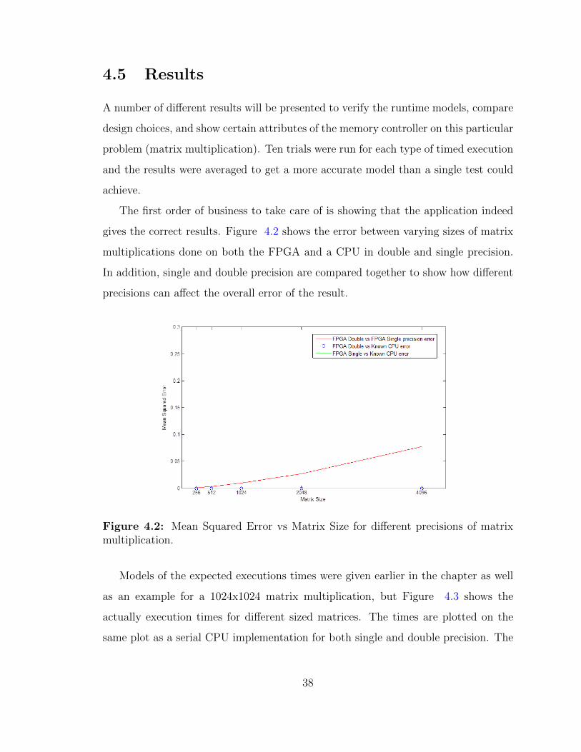
The first order of business to take care of is showing that the application indeed
gives the correct results. Figure 4.2 shows the error between varying sizes of matrix
multiplications done on both the FPGA and a CPU in double and single precision.
In addition, single and double precision are compared together to show how different
precisions can affect the overall error of the result.
Figure 4.2: Mean Squared Error vs Matrix Size for different precisions of matrixmultiplication.
Models of the expected executions times were given earlier in the chapter as well
as an example for a 1024x1024 matrix multiplication, but Figure 4.3 shows the
actually execution times for different sized matrices. The times are plotted on the
same plot as a serial CPU implementation for both single and double precision. The
38
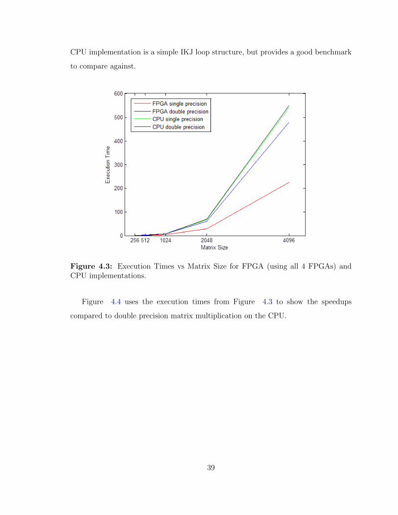
CPU implementation is a simple IKJ loop structure, but provides a good benchmark
to compare against.
Figure 4.3: Execution Times vs Matrix Size for FPGA (using all 4 FPGAs) andCPU implementations.
Figure 4.4 uses the execution times from Figure 4.3 to show the speedups
compared to double precision matrix multiplication on the CPU.
39
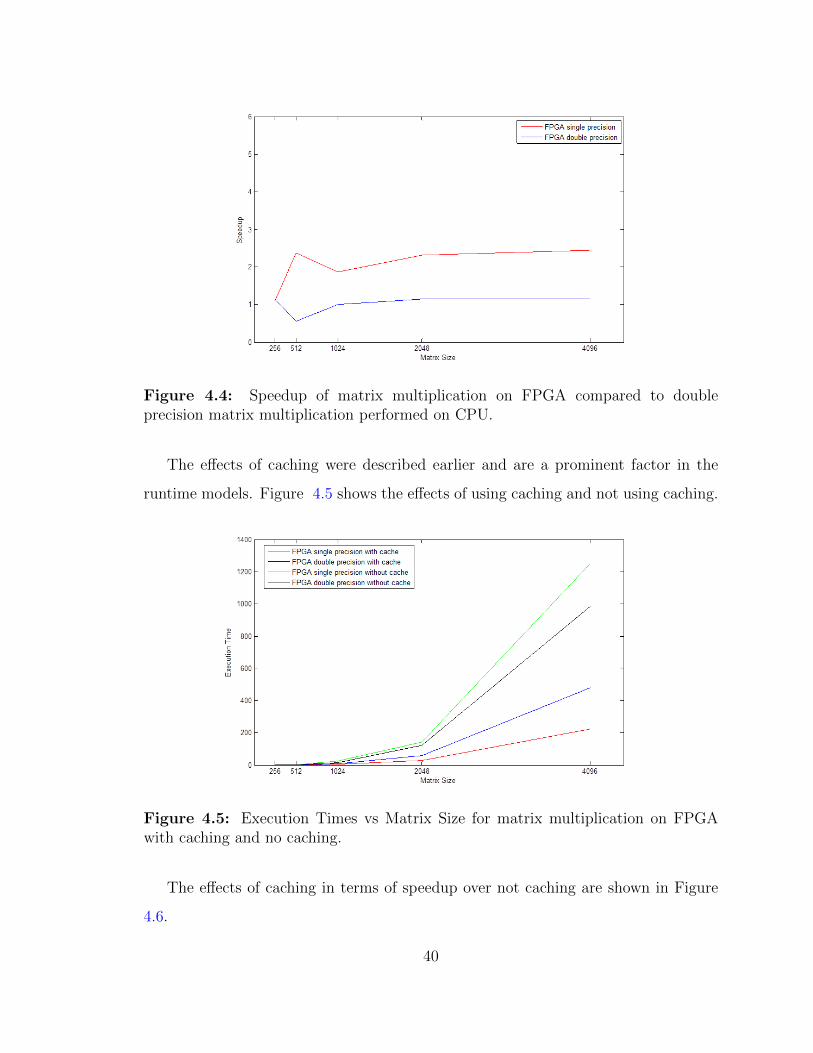
Figure 4.4: Speedup of matrix multiplication on FPGA compared to doubleprecision matrix multiplication performed on CPU.
The effects of caching were described earlier and are a prominent factor in the
runtime models. Figure 4.5 shows the effects of using caching and not using caching.
Figure 4.5: Execution Times vs Matrix Size for matrix multiplication on FPGAwith caching and no caching.
The effects of caching in terms of speedup over not caching are shown in Figure
4.6.
40
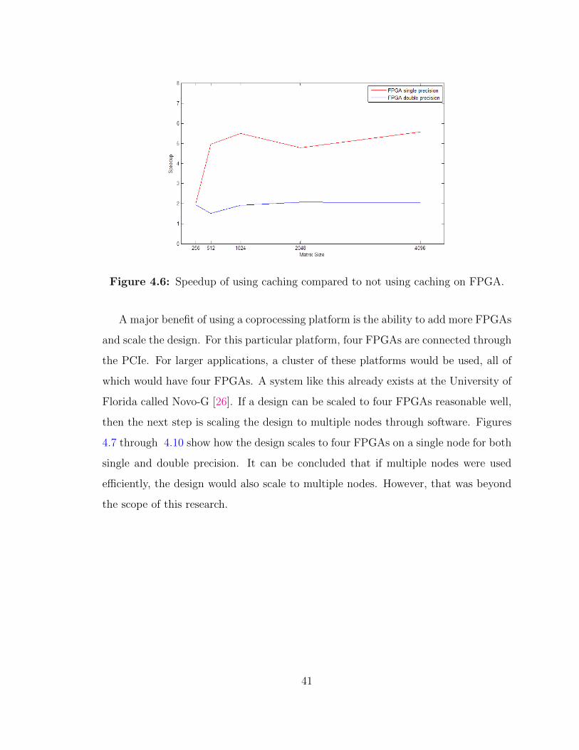
Figure 4.6: Speedup of using caching compared to not using caching on FPGA.
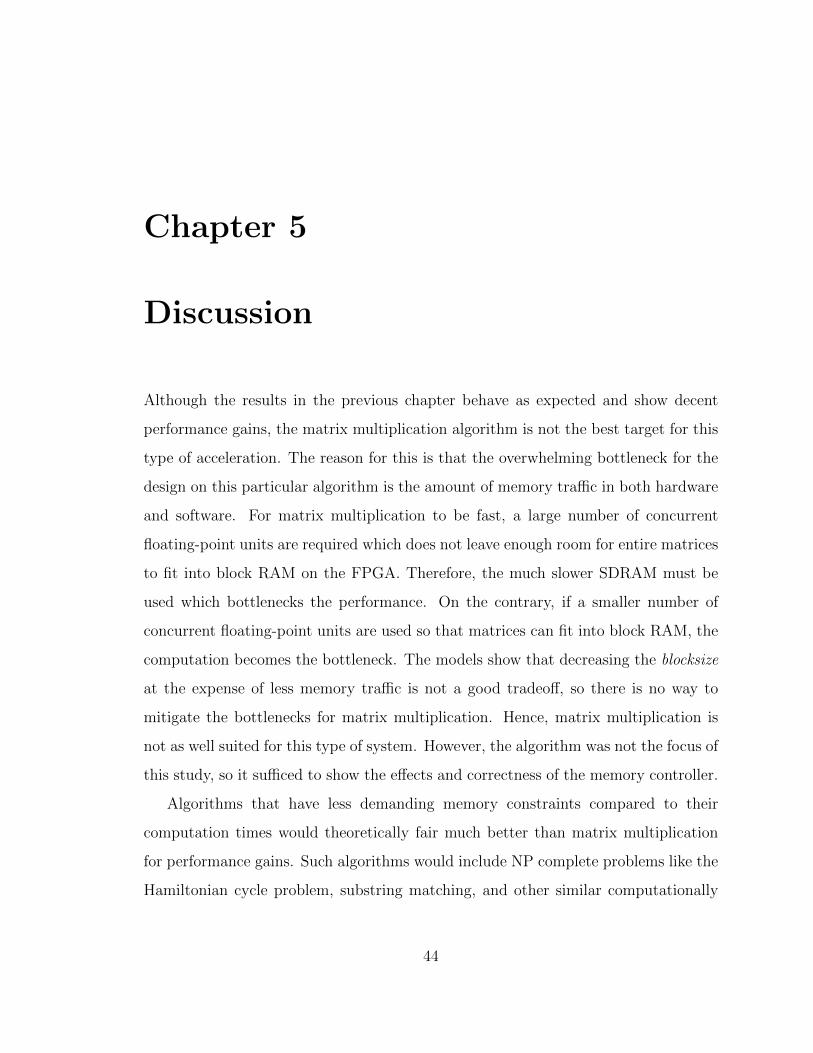
A major benefit of using a coprocessing platform is the ability to add more FPGAs
and scale the design. For this particular platform, four FPGAs are connected through
the PCIe. For larger applications, a cluster of these platforms would be used, all of
which would have four FPGAs. A system like this already exists at the University of
Florida called Novo-G [26]. If a design can be scaled to four FPGAs reasonable well,
then the next step is scaling the design to multiple nodes through software. Figures
4.7 through 4.10 show how the design scales to four FPGAs on a single node for both
single and double precision. It can be concluded that if multiple nodes were used
efficiently, the design would also scale to multiple nodes. However, that was beyond
the scope of this research.
41
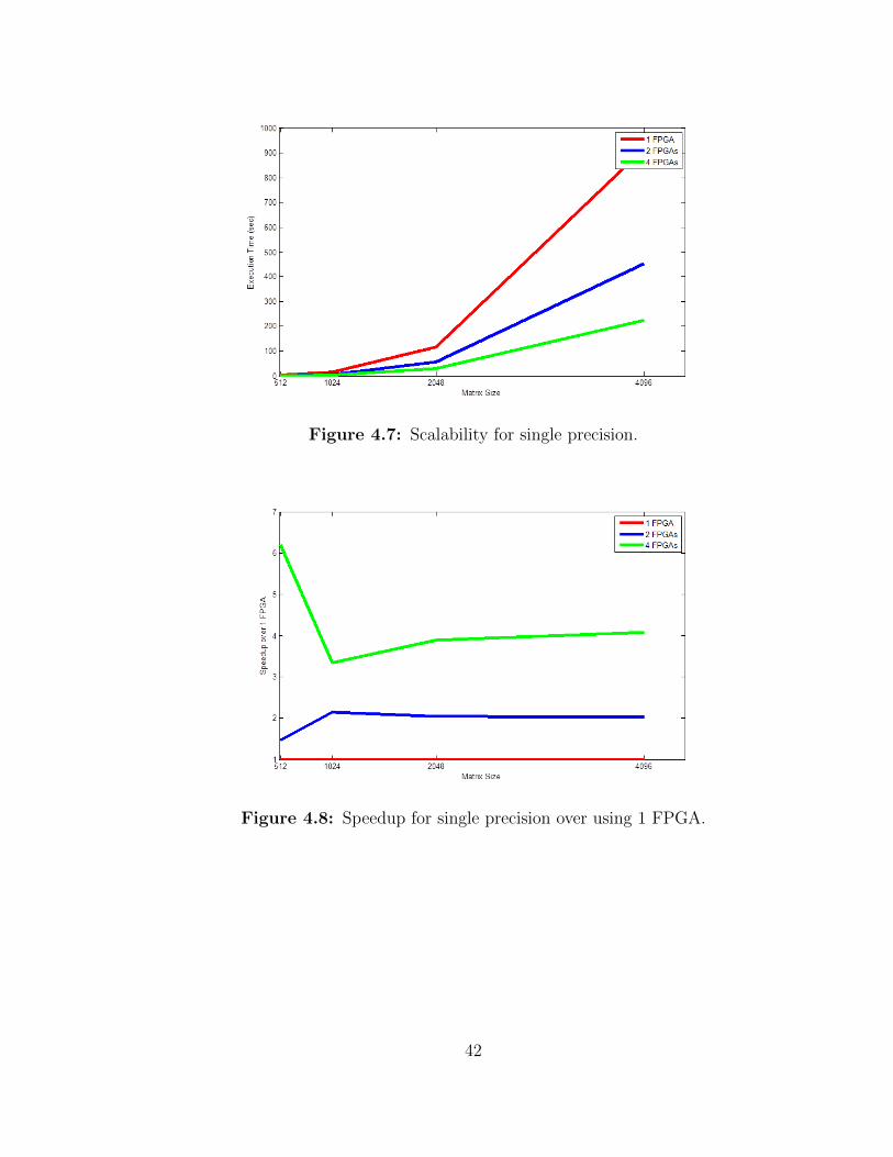
Figure 4.7: Scalability for single precision.
Figure 4.8: Speedup for single precision over using 1 FPGA.
42

Figure 4.9: Scalability for double precision.
Figure 4.10: Speedup for double precision over using 1 FPGA.
43
Chapter 5
Discussion
Although the results in the previous chapter behave as expected and show decent
performance gains, the matrix multiplication algorithm is not the best target for this
type of acceleration. The reason for this is that the overwhelming bottleneck for the
design on this particular algorithm is the amount of memory traffic in both hardware
and software. For matrix multiplication to be fast, a large number of concurrent
floating-point units are required which does not leave enough room for entire matrices
to fit into block RAM on the FPGA. Therefore, the much slower SDRAM must be
used which bottlenecks the performance. On the contrary, if a smaller number of
concurrent floating-point units are used so that matrices can fit into block RAM, the
computation becomes the bottleneck. The models show that decreasing the blocksize
at the expense of less memory traffic is not a good tradeoff, so there is no way to
mitigate the bottlenecks for matrix multiplication. Hence, matrix multiplication is
not as well suited for this type of system. However, the algorithm was not the focus of
this study, so it sufficed to show the effects and correctness of the memory controller.
Algorithms that have less demanding memory constraints compared to their
computation times would theoretically fair much better than matrix multiplication
for performance gains. Such algorithms would include NP complete problems like the
Hamiltonian cycle problem, substring matching, and other similar computationally
44

intensive problems [21, 22, 23, 24]. The reason for this is because matrix multiplication
has a computational complexity of O(n3), but its memory complexity is O(n2). The
size, n, needs to be large to warrant acceleration for matrix multiplication which
means the memory footprint is too large to fit entirely on the FPGA. However, with
an algorithm of higher computational complexity, say O(2n), n does not have to
be very large to warrant acceleration. The memory footprint fits entirely into the
FPGA and the acceleration has no major bottlenecks. Therefore, the SDRAM is
only needed to initially read the values onto the FPGA, and does not need to be
continuously referenced.
The performance benefits of using an FPGA as a coprocessor have been thoroughly
explored and shown, but there is still another alluring quality that using an FPGA
presents. FPGAs are well-documented for their low energy consumption because they
operate at slower clock rates [5, 9], while CPUs run at substantially higher clock rates
and consume more power. For this reason, FPGAs are targetted by applications that
require less power consumption than can be achieved through CPUs.
45
Chapter 6
Conclusion
The research presented in this thesis discussed the design and implementation
of a memory controller for FPGA applications that use floating-point numbers.
In particular, the memory controller was designed to be flexible for all floating-
point representations, scalable to any number of FPGAs, user-friendly for target
applications, and fast for memory transactions that are usually slow. These design
objectives were confirmed by performing tests with different parameters applied to
a target application, matrix multiplication. In conclusion, the results were excellent
for every aspect of the memory controller. However, the performance results could
have been much higher if a different target application were used as stated in the
Discussion chapter.
46
Chapter 7
Related Work
The related work that I completed alongside my thesis dealt with computer security.
I worked closely with Dr. Gregory D. Peterson and Dr. Nathanael Paul to perform
this research and submit a paper to the National Security Innovation Competition.
We received 11th place in this competition. The sections below summarize the paper
that was submitted for the competition.
Remote identification and authentication are challenging issues often solved
by password-based systems. Because adversaries can often guess user passwords,
a second step of a login process is used. Today, two-factor authentication is
an established method of identity management. Instead of solely relying on
authentication through something that you know (e.g., a password), an additional
login requirement must be met including (1) something that you have (e.g., a token-
generated value) or (2) something that you are (e.g., a fingerprint). Each of these
three authentication approaches is independent; a failure in one is independent of
another.
These types of two-factor systems have now been largely deployed and were
believed to be secure until recent attacks on one of the largest manufacturers
in March 2011. At that time, EMCs RSA companys SecureID hardware tokens
were compromised, and approximately all 40 million of its tokens needed (or need)
47

replacement [28]. Many companies use these tokens for secure logins. A company will
issue a hardware token for each of its users (e.g., a hardware device that is typically
kept on a keychain), and the user will use a password and the tokens computed values
for logging into a remote machine. The token will compute and display a new value
every 30 seconds. This increases authentication security, because the only devices
that can compute the token-generated values are the token and the authentication
server to check for valid logins. Our approach mitigates the damage from a potential
attack and facilitates simpler, cheaper recovery. While our primary example is the
well-known RSA two-factor authentication hardware token system (has 50% of the
market with 40 million customers [29]), the architecture is generally applicable to
two-factor authentication systems in general. Our system uses custom circuitry to
perform token-based authentication, but with additional policies implemented to limit
vulnerability to previously employed classes of attacks.
In March 2011, RSA employees received phishing email that contained malware.
In this email, the attacker used a zero-day flash vulnerability that was embedded
in a Microsoft document [31]. This malware successfully defeated the token-based
authentication system, but the specific details of how this happened have not been
revealed. A token generates a new token value by computing a function as shown in
Figure 7.1. The user supplies a userid, password, PIN code, and token code (i.e.,
login data), and the authentication server (at right) checks the login data by using
the secret key to generate and check the supplied login data.
48

Figure 7.1: Authentication with Traditional Two-factor Hardware Security Tokens.[30]
As long as the secret key is kept secret and authentication servers are synchronized
with the user tokens, then the system can authenticate users. Thus, replacing tokens
only must be done when secret keys are compromised, or a large amount of future
token values are revealed. If the tokens are not replaced, then an adversary could use
computed or stored token values to login as someone else if the attacker knew or could
break the password. In the March 2011 security breach, L-3 and Lockheed Martin
both blame their respective security breaches on this RSA token breach [33]. We must
assume that either the secret key for the RSA SecurID tokens were compromised, or
a large amount of future token values were compromised.
Our goal in this work is to mitigate attacks where a remote adversary learns login
information (i.e., secret key or future token values). We accomplish this through using
the token generation server to artificially delay token values to an authentication
server. Figure 7.2 shows our changed design for key management and token value
management. The authentication server requests a token value whenever a user
attempts to login. If a new token value has not been requested for a specified user
within the last time period, t, then the new token authentication value is released by
the token management device. If a token value has been released for a user within
a time period t, then the previous token value is released. To ensure that a remote
adversary cannot compromise the key or future token values, the delay for this time
49
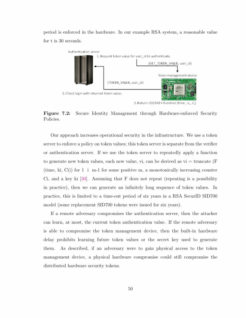
period is enforced in the hardware. In our example RSA system, a reasonable value
for t is 30 seconds.
Figure 7.2: Secure Identity Management through Hardware-enforced SecurityPolicies.
Our approach increases operational security in the infrastructure. We use a token
server to enforce a policy on token values; this token server is separate from the verifier
or authentication server. If we use the token server to repeatedly apply a function
to generate new token values, each new value, vi, can be derived as vi = truncate (F
(time, ki, Ci)) for 1 i m-1 for some positive m, a monotonically increasing counter
Ci, and a key ki [30]. Assuming that F does not repeat (repeating is a possibility
in practice), then we can generate an infinitely long sequence of token values. In
practice, this is limited to a time-out period of six years in a RSA SecurID SID700
model (some replacement SID700 tokens were issued for six years).
If a remote adversary compromises the authentication server, then the attacker
can learn, at most, the current token authentication value. If the remote adversary
is able to compromise the token management device, then the built-in hardware
delay prohibits learning future token values or the secret key used to generate
them. As described, if an adversary were to gain physical access to the token
management device, a physical hardware compromise could still compromise the
distributed hardware security tokens.
50
To demonstrate a proposed protection scheme against physical hardware compro-
mise, we assume that each token uses a unique key to generate token values for
one year (the time period is arbitrary). For keys used in year two, we encrypt
them until they are needed. A hardware compromise would then yield, at most,
one years worth of token values (i.e., the keys used to generate those token values).
The encryption keys used to encrypt the token-generating keys can be split using a
threshold cryptographic scheme. For example, if each year of a tokens lifespan was
encrypted with a key split into multiple parts, then a collusion between the holders of
these key parts would be needed for reassembly. Once these keys were reassembled,
the token-generating keys could be decrypted and used for each subsequent year.
The parties holding the future keys to unlock later authentication codes could
involve multiple parties at the manufacturer, or it could involve parties at user
organizations. With these added parties involved in the authentication process, the
threshold cryptographic storage of keys adds additional complexity. Key parts could
be mislabeled (e.g., year 2 could be switched with year 3) and extra management
is needed to reassemble keys. However, this will be an attractive solution, even
if only done for some subset of the user population. Given that these token
authentication schemes are used to defend access to critical data, involving multiple
parties that include the token manufacturer, the users, and government officials help
further protect future token values by requiring collusion across organizations for key
assembly.
With this new approach, recovery is now made possible. Assume that a remote
adversary gains physical access to a token management device. Once this is detected,
all token values that would be generated for the next calendar year are compromised
(i.e., the keys used to generate those values have been compromised). If we can
force tokens to switch to a new token-generating key early, then this avoids great
costs. To do this, we augment current tokens with a new feature that can reset the
token-generating key that also synchronizes with the token management device. One
51
possible way of doing this is through a hardware button where a user presses the
button according to some specified sequence to switch to a new key.
This architecture now enables new security guarantees. If an attacker were to
remotely compromise a device that receives a token value from a token generating
device, the attacker can only read a value every t time units. The hardware delay
cannot be circumvented remotely. This increases two-factor authentication security by
moving the key to a location that should only be compromised under physical access
(assuming that predicting future token values is computationally infeasible without
the key used to generate those values). We can quantify how many token values an
attacker can have obtained by computing how many values have been released from
the time of compromise. For example, if a compromise was a result of a particular
email, we know that the earliest point of compromise could not have happened before
the first SPAM email was delivered. To be safe, a new token-generating key can be
used by switching to a future time period (e.g., an early switch to year ks token-
generating key is made before the end of year k-1). This is accomplished through the
reassembling of the token-generation key.
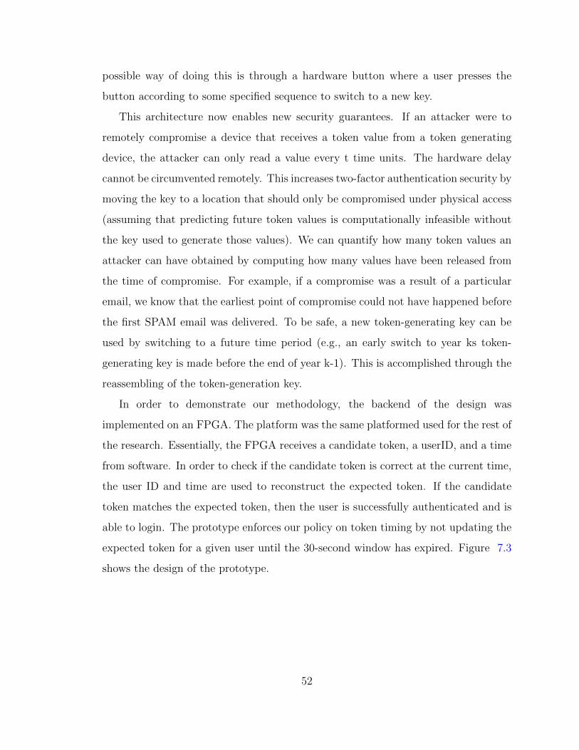
In order to demonstrate our methodology, the backend of the design was
implemented on an FPGA. The platform was the same platformed used for the rest of
the research. Essentially, the FPGA receives a candidate token, a userID, and a time
from software. In order to check if the candidate token is correct at the current time,
the user ID and time are used to reconstruct the expected token. If the candidate
token matches the expected token, then the user is successfully authenticated and is
able to login. The prototype enforces our policy on token timing by not updating the
expected token for a given user until the 30-second window has expired. Figure 7.3
shows the design of the prototype.
52
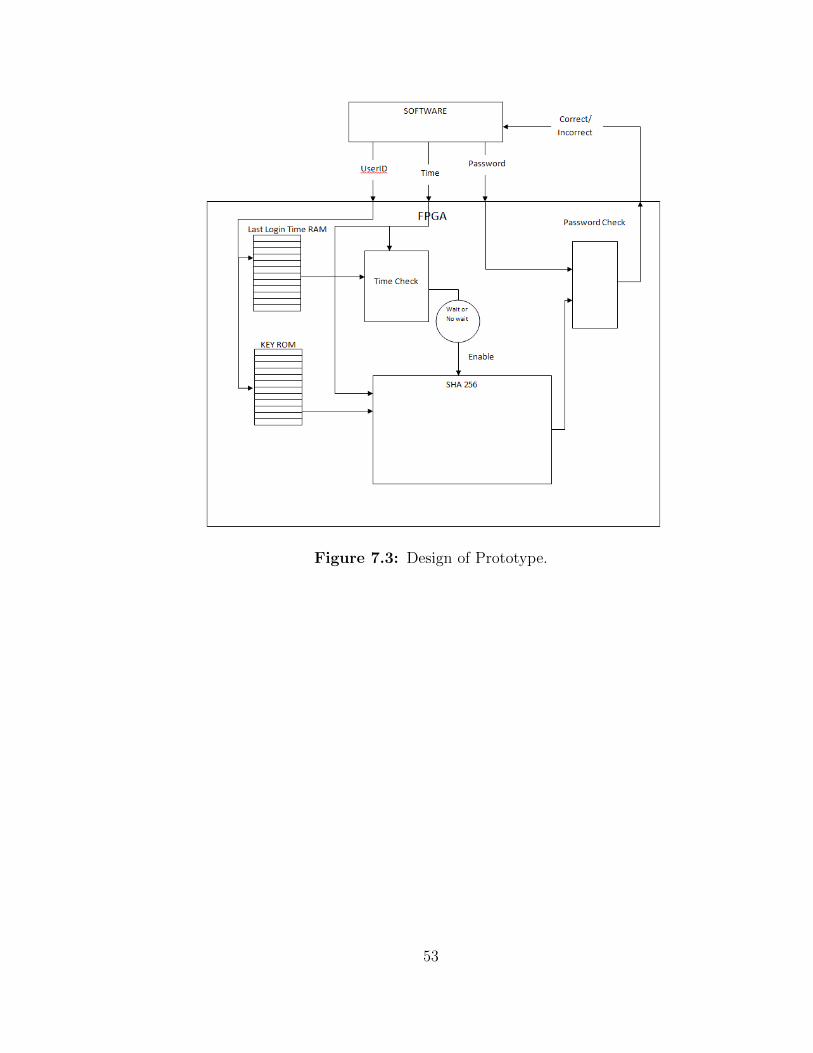
Figure 7.3: Design of Prototype.
53

Bibliography
54
Bibliography
[1] Pong P. Chu, ”FPGA Prototyping by VHDL Examples: Xilinx Spartan-3
Version”, John Wiley & Sons, Inc., 2008.
[2] Hartmut F.-W. Sadrozinski and Jinyuan Wu, ”Applications of Field-
Programmable Gate Arrays in Scientific Research”, Taylor & Francis, 2010. 1
[3] Levinson H. Simmle and Reinhard Manner, ”Multitasking on FPGA
Coprocessors”, FPL ’00 Proceedings of the The Roadmap to Reconfigurable
Computing, 10th International Workshop on Field-Programmable Logic and
Applications, 2000, pp. 121–130. 1
[4] G. Govindu, L. Zhuo, S. Choi, and V. Prasanna. ”Analysis of High-performance
Floating-point Arithmetic on FPGAs”. In Proceedings of the 18th International
Parallel and Distributed Processing Symposium (IPDPS04), pages 149156, April
2004.
[5] J. Jang, S. Choi, and V. K. Prasanna, ”Energy-Efficient Matrix Multiplication
on FPGAs”. In Proceedings of the 12th International Workshop on Field
Programmable Logic and Application (FPL 2002), pages 534544. LNCS 2438,
August 2002. 45
[6] J. Jang, S. Choi, and V. K. Prasanna. ”Area and Time Efficient Implementations
of Matrix Multiplication on FPGAs”. In Proceedings of the IEEE International
Conference on Field-Programmable Technology (FPT 2002), pages 93100,
December 2002.
55
[7] G. Lienhart, A. Kugel, and R. Manner. ”Using Floating-Point Arithmetic on
FPGAs to Accelerate Scientific N-Body Simulations”. In Proceedings of the IEEE
Symposium on Field-Programmable Custom Computing machines (FCCM 2002),
pages 182191, April 2002.
[8] W. B. Ligon III, S. McMillan, G. Monn, K. Schoonover, F. Stivers, and K. D.
Underwood. ”A Re-evaluation of the Practicality of Floating-Point Operations on
FPGAs”. In Proceedings of the IEEE Symposium on Field-Programmable Custom
Computing machines (FCCM 1998), pages 206215, April 1998.
[9] R. Scrofano, S. Choi, and V. K. Prasanna. ”Energy Efficiency of FPGAs and
Programmable Processors for Matrix Multiplication”. In Proceedings of the IEEE
International Conference on Field-Programmable Technology (FPT 2002), pages
422425, December 2002. 45
[10] GiDEL, ”Proc API”, Data Book, 2012. 4
[11] GiDEL, ”ProcWizard”, User’s Manual Version 8.8, 2010. 3
[12] GiDEL, ”ProcMultiport IP SDRAM Controller”, User’s Guide, 2011. viii, 4, 7,
8
[13] Altera, ”Floating-Point Megafunctions”, User Guide, 2011.
[14] Altera, ”Accelerating High-Performance Computing with FPGAs”, Altera White
Paper, 2007. 1
[15] Lattice Semiconductor, ”Developing High-speed Memory Interfaces: The
LatticeSCM FPGA Advantage”, A Lattice Semiconductor White Paper,
February 2006.
[16] Ashley Brown, Paul Kelly, and Wayne Luk, ”Profiling floating point value ranges
for reconfigurable implementation”, Proceedings of the 1st HiPEAC Workshop on
Reconfigurable Computing, Ghent, Belgium, January 2007. 1
56

[17] Haru Shimada and Akinori Kanasugi, ”A Dynamically Reconfigurable
Arithmetic Circuit for Complex Number and Double Precision Number”, World
Academy of Science, Engineering and Technology, Vol. 54, 2009.
[18] Michael Lam, Jeffrey Hollingsworth, and Akinori Kanasugi, ”Dynamic
Floating-Point Cancellation Detection”, First International Workshop on High-
performance Infrastructure for Scalable Tools, Tuscon AZ, June 2011.
[19] Nirav Dave , Kermin Fleming, Myron King, Michael Pellauer, and Muralidaran
Vijayaraghavan, ”Hardware Acceleration of Matrix Multiplication on a Xilinx
FPGA”, Computer Science and Artificial Intelligence Lab, Massachusetts
Institute of Technology.
[20] P. M. Zhong, Martonosi, P. Ashar, and S. Malik, Using Configurable Computing
to Accelerate Boolean Satisfiability, IEEE Transactions on CAD of Integrated
Circuits and Systems, vol. 18, No. 6, June 1999.
[21] K. B. Kent, S. Van Schaick, J. E. Rice, and P. A. Evans, ”Hardware-based
implementation of the common approximate substring algorithm, Digital System
Design, 2005. Proceedings. 8th Euromicro Conference, September 2005. 45
[22] K. B. Kent and M. Serra, Using FPGAs to Solve the Hamiltonian Cycle Problem,
International Symposium on Circuits and Systems (ISCAS) 2003, May 2003. 45
[23] K. B. Kent and M. Serra, Using Instance-Specific Circuits to Compute
Autocorrelation Coefficients, First Northeast Workshop on Circuits and Systems,
2003. 45
[24] K. B. Kent, B. C. Iaderoza, and M. Serra, ”Codesign of a Computationally
Intensive Problem in GF(3)”, Rapid Systems Prototyping, 2007. RSP 2007. 18th
IEEE/IFIP International Workshop, May 2007. 45
[25] Manuel Jimenez, Nayda Santiago, and Diane Rover, ”Development of a Scalable
FPGA-Based Floating Point Multiplier”, December 1995.
57
[26] Novo-G: Adaptively Custom Research Supercomputer. Retrieved June 7, 2012
from http://www.chrec.org/facilities.html. 41
[27] Battle.net Authenticator. Blizzard Entertainment. Available at http://us.
blizzard.com/store/search.xml?q=authenticator.
[28] Siobhan Gorman and Ghara Tibken. ”Security Tokens Take Hit”. The Wall Street
Journal. June 7, 2011. 48
[29] Rachael King. ”EMC’s RSA Security Breach May
Cost Bank Customers 100 Million”. Bloomberg.
Available at http://www.bloomberg.com/news/2011-06-08/
emc-s-rsa-security-breach-may-cost-bank-customers-100-million.
html. 48
[30] D. M’Raihi, S. Machani, M. Pei, and J. Rydell. ”TOTP: Time-Based One-
Time Password Algorithm”. Internet Engineering Task Force (IETF) Request
for Comments 6238, May 2011. ix, 49, 50
[31] Uri Rivner. ”Anatomy of an Attack.” Speaking of Security: The Offi-
cial RSA Blog and Podcast. Available at http://blogs.rsa.com/rivner/
anatomy-of-an-attack. 48
[32] Keith Stuart. ”PlayStation hack: network will be back in
days, says Sony.” theguardian. April 28, 2011. Available at
http://www.guardian.co.uk/technology/gamesblog/2011/apr/28/
playstation-hack-network-sony-psn.
[33] Jaikumar Vijayan. ”Cyberattacks fuel concerns about RSA SecurID breach.”
Computerworld. June 1, 2011. Available at http://www.computerworld.com/
s/article/9217216/Cyberattacks_fuel_concerns_about_RSA_SecurID_
breach. 49
58
Vita
Bryan Jacob Hunter was born in Nashville, TN on 3 March 1988. He graduated from
Mt. Juliet High School in 2006 where he went on to the University of Tennessee in
Knoxville, TN. He received his Bachelor of Science in Electrical Engineering in May
2010. He continued his education at UTK where he is currently pursuing his Master
of Science degree in Computer Engineering.
59