Embed Size (px)
Citation preview
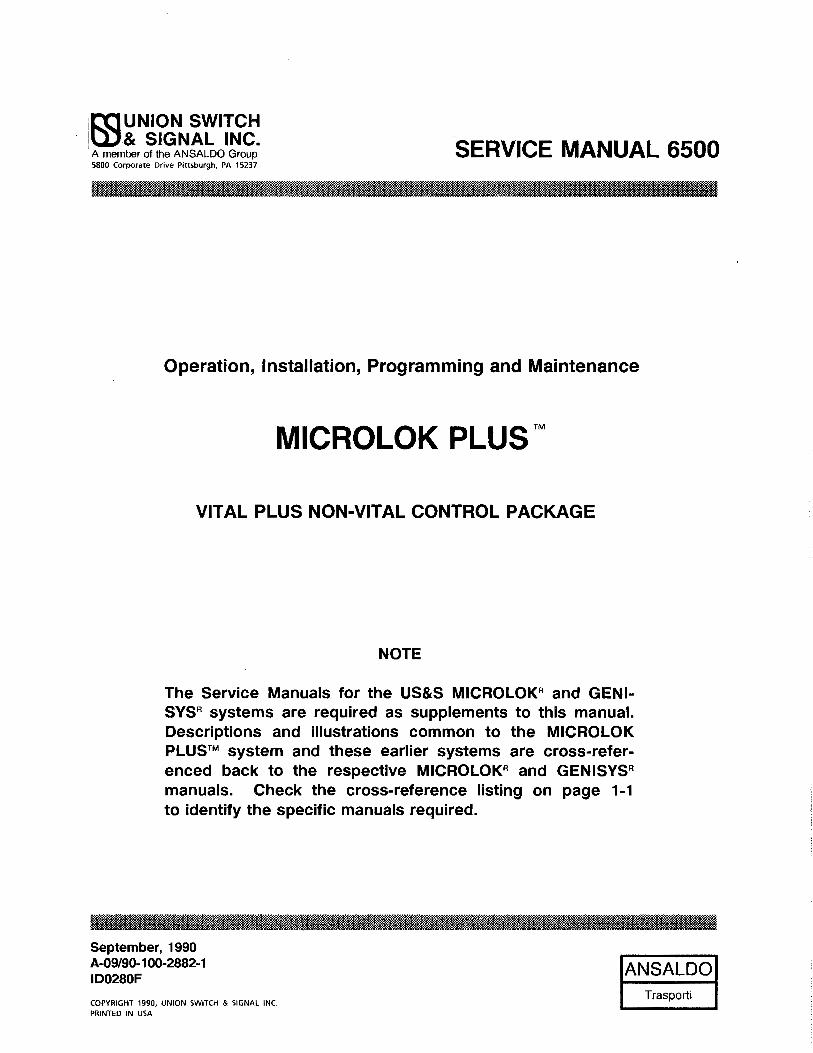
00 UNION SWITCH llJ & SIGNAL INC. A member of the ANSALDO Group 5800 Corporate Drive Pittsburgh, PA 15237
SERVICE MANUAL 6500
Operation, Installation, Programming and Maintenance
MICROLOK PLUS TM
VITAL PLUS NON-VITAL CONTROL PACKAGE
NOTE
The Service Manuals for the US&S MICROLQKR and GENISVSR systems are required as supplements to this manual. Descriptions and illustrations common to the MICROLOK PLUS™ system and these earlier systems are cross-referenced back to the respective MICROLOKR and GENISVSR manuals. Check the cross-reference listing on page 1-1 to identify the specific manuals required.
September, 1990 A-09/90-100-2882-1 ID0280F
AN SAL DO
COPYRIGHT 1990, UNION SWITCH & SIGNAL INC. PRINTED IN USA
Trasporti
Revised and new pages of this manual are listed by page number and date:
Page No. Date Page No. Date
Section
I GENERAL 1.1 1.2 1. 2 .1 1.2.2 1. 2 .3 1. 2. 4 1.2.4.1 1.2.4.2 1. 2. 5 1.2.5.1 1.2.5.2 1. 2. 6 1.3 1.3.1 1. 3. 2 1.3.2.1 1.3.2.2 1.3.2.3 1.3.2.4 1.3.2.5 1.4 1.4.1 1. 4. 2 1.5 1. 5.1 1. 5.2 1.5.2.1 1.5.2.2 1.5.2.3 1.5.3 1. 5.4
CONTENTS
INFORMATION PURPOSE AND SCOPE OF MANUAL INTRODUCTION General Vital Section Basic Functions Non-Vital Section Basic Functions Serial Data Systems Vital Section Non-Vital Section Executive and Application Software Application Executive Power Requirements and Applications HARDWARE DESCRIPTION Card file Plug-In Printed Circuit Boards General Arrangement Vital CPU PCBs Vital I/0 PCBs Non-Vital Controller PCB Non-Vital I/0 PCBs AUXILIARY EQUIPMENT Vital Cut-Off Relay (VCOR) Serial Communications Adapter Panel SPECIFICATIONS Physical/Mechanical Electrical Power Supply converter Vital I/0 PCBs Non-Vital I/0 PCBs Environmental Miscellaneous
II INSTALLATION 2.1 SHIPMENT HANDLING 2.2 UNIT MOUNTING AND ENVIRONMENT 2.3 FACILITY WIRING 2.4 POWER AND GROUND CIRCUITS 2.4.1 Power Sources 2.4.2 Wiring and Surge/Noise Protection 2.4.3 Equipment Grounding 2.4.3.1 Rack and Cardfile Grounding 2.4.3.2 O Volts Connection to Earth Ground 2.4.3.3 Serial and Local Cable Connection to 2.4.4 Power Supply 5 Volt Adjustment 2.4.5 Auxiliary Power for RFL Modem 2.5 PCB PREPARATION 2.5.1 Vital CPU 2.5.2 Vital I/0 2.5.3 Non-Vital Controller
i
1-1 1-1 1-2 1-2 1-2 1-4 1-4 1-4 1-6 1-6 1-6 1-7 1-8 1-8 1-8 1-10 1-10 1-11 1-11 1-12 1-12 1-13 1-13 1-13 1-13 1-13 1-14 1-14 1-15 1-15 1-15 1-15
2-1 2-1 2-1 2-1 2-2 2-2 2-2 2-4 2-4 2-4
Earth Ground 2-4 2-6 2-7 2-7 2-7 2-7 2-8
CONTENTS (Cont'd)
Section
2.5.4 2.6 2.7 2.8 2.9 2.9.1 2.9.2 2.9.3 2.9.4 2.9.5 2.9.6 2.10 2 .11
Non-Vital I/0 PCBs PCB INSTALLATION ECHO ENABLE JUMPERS (VITAL I/0) VITAL SECTION LOCAL INTERFACES VITAL SECTION SERIAL INTERFACES Serial Ports Cabling General Notes Modem Recommendations Vital Master and Satellite EIA Interfaces Vital Section - Code System Interface current Loop Interface NON-VITAL SECTION LOCAL INTERFACES NON-VITAL SECTION SERIAL INTERFACE SPECIFICATIONS
III FUNCTIONAL DESCRIPTION 3.1 VITAL SECTION 3.2 NON-VITAL SECTION
IV APPLICATION PROGRAMMING
v
4.1 VITAL SECTION 4.2 NON-VITAL SECTION
FIELD MAINTENANCE 5.1 VITAL SECTION 5.1.1 General Requirements 5.1.2 Periodic Inspection 5.1.3 Troubleshooting Guide 5.1.3.1 Required Test Equipment and Materials 5.1.3.2 Power-Off Checks 5.1.3.3 Power-On Checks 5.1.3.4 5.1.3.5 5.1.3.6
5.1.3.7 5.1.3.8 5.1.4 5.2 5.2.1 5.2.2 5.2.2.1 5.2.2.2 5.2.2.3 5.3
Power-On System Tests Displaying and Clearing Error Codes Reading Error Codes, Error Code Descriptions and Troubleshooting PCB Descriptions Code System Interface Troubleshooting Retesting Guidelines NON-VITAL SECTION Basic Maintenance Systematic Troubleshooting Introduction Recommended Test and Repair Equipment Initial Checks and Diagnostics Via Board LEDs POWER SUPPLY DRAWER
VI SHOP MAINTENANCE 6.1 VITAL SECTION PCBS 6.2 NON-VITAL SECTION PCBS 6.3 POWER SUPPLY DRAWER
ii
2-8 2-8 2-8 2-9 2-10 2-10 2-10 2-12 2-12 2-14 2-16 2-16 2-17/18
3-1 3-1 3-1
4-1 4-1 4-3
5-1 5-1 5-1 5-1 5-1 5-1 5-2 5-2 5-3 5-3 5-5
5-7 5-9 5-9 5-10 5-10 5-10 5-10 5-10 5-11 5-13/14
6-1/2 6-1/2 6-1/2 6-1/2
CONTENTS (Cont'd)
Section
APPENDIX A A.1
PARTS LIST CARDFILE N451796-0102 A-2
A.2 A. 3 A.3.1 A.3.2 A.3.2.1 A.3.2.2
A.5 A.6 A.7
PLUG-IN PRINTED CIRCUIT BOARDS A-4 VITAL SECTION SERIAL LINK CABLE ASSEMBLIES A-5 Complete Assemblies A-5 Standard Components A-6 37-Pin D Connector/Cable Assemblies (Master/Satellite) A-6 Cable Assembly: Vital Code System Port to Non-Vital A-7 Controller VITAL SECTION LOCAL I/0 CABLE ASSEMBLIES A-8 NON-VITAL SECTION SERIAL AND LOCAL CABLE ASSEMBLIES A-8 DEVELOPMENT SYSTEM HARDWARE AND SOFTWARE A-8
APPENDIX B KEY COMPARISONS OF MICROLOK PLUS, MICROLOK, GENISYS
Figure
1-1
1-2
1-3
1-4
2-1
2-2
2-3
2-4
2-5
2-6
3-1
4-1
4-2
4-3
ILLUSTRATIONS
Basic Configuration and Applications
Serial Communication System Configurations
Application and Executive Software
Cardfile General Design and PCB Arrangements
Typical MICROLOK PLUS Power Input Wiring
Summary of MICROLOK PLUS Ground Circuits
Power Supply 5 Volt Output Check and Adjustment
Echo Enable Jumper Position Check
Serial Data Ports and Cables
Standard MICROLOK PLUS Vital Section/Non-Vital Interface
Vital Section serial Link to Non-Vital controller
Sample for Source Listing MICROLOK PLUS Vital Section Application Program
Sample Symbol Table for MICROLOK PLUS Vital Section Application Program
Sample Source Listing for MICROLOK PLUS Non-Vital Section Application Program
iii
1-3
1-5
1-7
1-9
2-3
2-5
2-6
2-9
2-11
2-15
3-2
4-2
4-3
4-6
Figure
4-4
5-1
5-2
5-3
A-1
A-2
ILLUSTRATIONS (Cont'd)
Sample Symbol Table for MICROLOK PLUS Non-Vital Section Application Program
Configuration of Vital Section LEDs
Typical Long Error Codes
Configuration of Non-Vital section LEDs
Cardfile Assembly
Code System/Controller Cable Assembly N451458-980X
MICROLOK PLUS Cardfile
vi
4-7/8
5-4
5-6
5-12
A-3
A-7
SECTION I GENERAL INFORMATION
1.1 PURPOSE AND SCOPE OF MANUAL
This manual provides and cross references information on the installation, programming, operation and field maintenance of the MICROLOK PLUS Vital and Non-Vital Control Package.
Because the MICROLOK PLUS system shares much of the hardware and software of the US&S MICROLOK and GENISYS systems, the service manuals for these other systems are extensively cross-referenced in this manual. Common descriptions and procedures are cited by section, and page number in the respective MICROLOK or GENISYS manual. If the MICROLOK PLUS system is only equipped with a vital section, the following US&S Service Manuals are required to supplement this manual (latest revision dates as of 8-1-90):
Manual No. & Rev. Date
SM-6400A (12/88)
SM-6400B ( 11/89)
SM-6400C (3/89)
Product
MICROLOK Vital Interlocking Control System
MICROLOK Vital Interlocking Control System
MICROLOK Vital Interlocking Control System
Scope
Application Logic Programming
Hardware Installation
Field Maintenance
If the MICROLOK PLUS system is equipped with a vital section and a non-vital section, the following US&S Service Manuals are also required to supplement this manual:
SM-6300A (7/89)
SM-6300B (6/90)
SM-6300C (9/88)
GENISYS Non-Vital Logic Emulator
GENISYS Non-Vital Logic Emulator
GENISYS Non-Vital Logic Emulator
Application Logic Programming
Hardware Installation and Field Maintenance
Shop Maintenance of Plug-In Printed Circuit Boards
Following is an example of the standard format for the cross-reference notations in this manual:
Subject
DC Lamp Driver PCB -Specifications
Topic covered in cross reference.
SM-6400B,
• US&S
Service Manual
No.
6500, p. 1-1
Cross Reference
section 2.8.2.2, page 2-25
• • Section Page no. Number or first in that page no. Manual of that
section
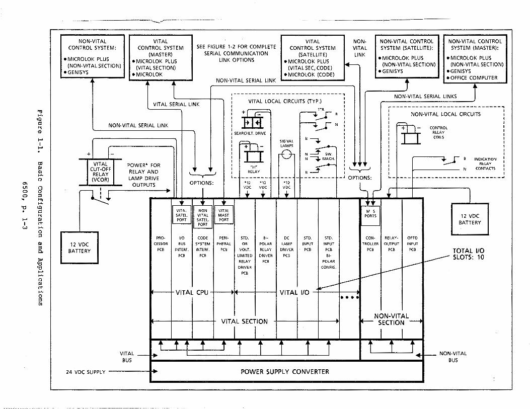
1.2 INTRODUCTION (See Figures 1-1 and 1-2)
1.2.1 General
The MICROLOK PLUS Vital and Non-Vital Control Package is a multi-purpose, microprocessor-based device designed for use in both vital and/or non-vital railroad control systems. It is typically used for smaller applications, such as a single end-of-siding, that do not require the large input/output capabilities of seperate vital and non-vital controllers. The device can be configured with a vital control section only, or with vital and non-vital control sections. (A non-vital-only configuration is also possible, but not typical.)
In a typical single end-of-siding application, both sections are utilized. The vital section controls the interlocking logic, manages switch machines, signals and track circuits in the control area; while the non-vital section provides an interface point for a local control panel, processes CTC office commands, and transmits indications from the vital section. Another typical end-of-siding configuration could consist of the vital section only, with code system inputs and outputs processed within the vital section (no local control panel).
The MICROLOK PLUS system is derived from the US&S MICROLOK Vital Interlocking Control System and the GENISYS Non-Vital Logic Emulator. It uses the same plug-in printed circuit boards (logic and interface), the same Executive software, and the same application logic compilers as the MICROLOK and GENISYS systems.
1.2.2 Vital Section Basic Functions
The vital section of MICROLOK PLUS unit is designed specifically for railroad vital interlocking applications. Its basic function is to process various inputs according to a program designed by the application engineer, and create the appropriate outputs. This program takes inputs, performs logic and timing functions on those inputs and produces an output. The program operates in the same manner as a conventional vital relay logic system.
Inputs and outputs consist of "local" and "serial". Local inputs typically include track circuit occupancy, state of switch machine point contacts, state of signal relay or mechanism contacts, and traffic and line circuits. Local outputs eventually interface to control signal mechanism drives, signal lamp drives, switch control contactors and traffic and line control circuits. Serial inputs and outputs typically carry vital and non-vital control and indication messages between the MICROLOK PLUS system and other vital and non-vital controllers, or between the vital and non-vital sections of the unit.
Local input options include standard off/on (bit 0/1) voltage inputs, or bi-polar voltage inputs (bit O or 1 for each polarity). Two voltage input ranges are available with these options: 12 or 24 Vdc (nominal). Local vital output options include standard (single pole) relay drive, or bi-polar relay drive. Lamp-compatible outputs are available to drive 18, 25 or 36 watt, 10 volt signal lamps.
6500, p. 1-2
'%J ..... lQ c t'1 CD
...... I ...... . 0, Ill Cll ..... n
°' u, (") 0 0 0 ::s ... Ht .....
'O lQ . c t'1
...... Ill I rt w .....
0 ::s Ill
5. > 'O 'O ...... ..... n Ill rt ..... 0 ::s Cll
NON-VITAL CONTROL SYSTEM:
• MICROLOK PLUS (NON-VITAL SECTION)
•GENISYS
...
.·....___,,.,,,-,
VITAL CONTROL SYSTEM
(MASTER) • MICROLOK PLUS
(VITAL SECTION) •MICROLOK
...
SEE FIGURE 1-2 FOR COMPLETE SERIAL COMMUNICATION
LINK OPTIONS
NON-VITAL SERIAL LINK
VITAL CONTROL SYSTEM
(SA TE LUTE) • MICROLOK PLUS
(VITAL SEC, CODE) • MICROLOK (CODE)
NONVITAL LINK
~
NON-VITAL CONTROL SYSTEM (SATELLITE):
• MICROLOK PLUS (NON-VITAL SECTION)
•GENISYS
j
NON-VITAL CONTROL SYSTEM (MASTER):
• MICROLOK PLUS (NON-VITAL SECTION)
•GENISYS •OFFICE COMPUTER
.----------------------------~ NON-VITAL SERIAL LINKS j
+
12 VDC BATTERY
VITAL SERIAL LINK
NON-VITAL SERIAL LINK
r-
VITAL II NON Ill VITAL SATEL. VITAL MAST. PORT SA TEL. PORT
PORT
PRO· 1/0 CODE PERI· STD. Bl· DC I STD.
CESSOR BUS SYSTEM PHERAL OR POLAR LAMP INPUT
PCB INTERF. INTERF. PCB VOLT. RELAY DRIVER PCB
PCB PCB LIMITED DRIVER PCB
RELAY PCB
DRIVER
PCB
N I VITAL CPU I •14 I I VITAL 1/0
VITAL SECTION
I I v:~~L --t. t ! t}~t ~~ j 1
STD.
INPUT
PCB
Bl·
POLAR
CONFIG.
j
24 VDC SUPPLY I llo POWER SUPPLY CONVERTER
. ••••
... •
~----------------------------~ NON-VITAL LOCAL CIRCUITS
M S PORTS
rB L- ... ---
CON· I RELA y. I OPTO TROLLER OUTPUT INPUT
PCB PCB PCB
a..__ NON-VITAL ...---- SECTION ____.
I I
CONTROL RELAY COILS
~B INDICATION RELAY
CONTACTS N
12 VDC BATTERY
TOTAL 1/0 SLOTS: 10
D ~ NON-VITAL
BUS
1.2.3 Non-Vital Section Basic Functions
The non-vital section of MICROLOK PLUS unit can perform the functions of various non-vital relay logic and digital logic systems, according to a program designed by the application engineer. This program takes inputs, performs logic and timing functions on those inputs and produces an output. The program operates in the same manner as a conventional non-vital relay logic system.
Inputs and outputs consist of •1ocal" and "serial•. Local inputs include all non-vital relay or switch contact signals, such as from a local control panel or code system field circuits. Local output options include internally strobed or non-strobed delivery and constant state at power off. Serial inputs and outputs typically carry non-vital control and indication messages between the MICROLOK PLUS system and other vital and non-vital controllers, or between the non-vital and vital sections of the unit.
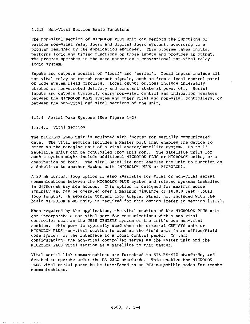
1.2.4 Serial Data Systems (See Figure 1-2)
1.2.4.1 Vital Section
The MICROLOK PLUS unit is equipped with •ports• for serially communicated data. The vital section includes a Master port that enables the device to serve as the managing unit of a vital Master/Satellite system. Up to 16 Satellite units can be controlled from this port. The Satellite units for such a system might include additional MICROLOK PLUS or MICROLOK units, or a combination of both. The vital Satellite port enables the unit to function as a Satellite to another Master unit (MICROLOK PLUS or MICROLOK).
A 20 mA current loop option is also available for vital or non-vital serial communications between the MICROLOK PLUS system and related systems installed in different wayside houses. This option is designed for maximum noise immunity and may be operated over a maximum distance of 10,000 feet (total loop length). A separate current Loop Adapter Panel, not included with the basic MICROLOK PLUS unit, is required for this option (refer to section 1.4.2).
When required by the application, the vital section of the MICROLOK PLUS unit can incorporate a non-vital port for communications with a non-vital controller such as the US&S GENISYS system or the unit's own non-vital section. This port is typically used when the external GENISYS unit or MICROLOK PLUS non-vital section is used as the field unit in an office/field code system, or the interface to a local control panel. In this configuration, the non-vital controller serves as the Master unit and the MICROLOK PLUS vital section as a Satellite to that Master.
Vital serial link communications are formatted to EIA RS-423 standards, and aerated to operate under the RS-232C standards. This enables the MICROLOK PLUS vital serial ports to be interfaced to an EIA-compatible modem for remote communications.
6500, p. 1-4
VITAL MASTER/SATELLITE SERIAL LINK - CENTRALIZED CONTROL (ALL EIA RS-423)
MASTER
VITAL SECTION
N-VITAL SECTION
MICROLOK PLUS
SATELLITE #1
VITAL SECTION
N-VITAL SECTION
MICROLOK PLUS
SATELLITE #2
VITAL SECTION
N-VITAL SECTION
MICROLOK PLUS
v SP
SATELLITE #3
MICROLOK (CPU)
UP TO 16
MICROLOK
PLUS AND/OR
MICROLOK
SATELLITES
VITAL MASTER/SATELLITE SERIAL LINK - DISTRIBUTED CONTROL (ALL EIA RS-423)
VITAL SECTION
N-VITAL SECTION
MICROLOK PLUS
VITAL SECTION
N-VITAL SECTION
MICROLOK PLUS
v v SP MP
MICROLOK (CPU)
CURRENT LOOP INTERFACE (VITAL LINK)
VITAL SECTION
N-VITAL SECTION
MICROLOK PLUS
r----------------------------1 r----------------------------1
VITAL SECTION
MASTER
VITAL SECTION
EIA RS-423
SERIAL COMM. ADAPTER
N-VITAL SECTION
MICROLOK PLUS
L----------------------------l
20 mA CURRENT LOOP
10,000 FT. CABLE LENGTH MAX.
(PER LOOP)
MICROLOK PLUS
VITAL SECTION
SA TEL
N-VITAL SECTION
L----------------------------NON-VITAL INTERFACES (INTERNAL AND EXTERNAL) TO VITAL SECTION (ALL EIA RS-423)
N-VITAL SECTION
VITAL SECTION
N-VITAL SECTION
VITAL SECTION
M S NVP
N-VITAL SECTION
VITAL SECTION
N-VllAL SECTION
M S NVP
MICROLOK PLUS MICROLOK PLUS MICROLOK PLUS MICROLOK PLUS GENISYS OR COMPUTER
INTERFACES TO NON-VITAL SECTION (EIA OR TTL)
MASTER SATELLITE tfl SATELLITE #2 SATELLITE #3
ABBREVIATIONS M S NVP
M S M S NVP
M S NVP
v SP
VITAL SATELLITE PORT
NV NON-VITAL P PORT
v MP
VITAL MASTER PORT
M S MASTER & SATEL. NVP NON-VITAL
PORTS
GENISYS OR COMPUTER
MASTER
VITAL SECTION
M S NVP
N-VITAL SECTION
MICROLOK PLUS
VITAL SECTION
NVP
N-VITAL SECTION
MICROLOK PLUS
SATELLITE #1
VITAL SECTION
M S NVP
N-VITAL SECTION
MICROLOK PLUS
VITAL SECTION
N-VITAL SECTION
MICROLOK PLUS
M S NVP
SATELLITE #2
GENISYS
VITAL SECTION
N-VITAL SECrlON
MICROLOK PLUS
UP TO 255 MICROLOK PLUS
AND/OR GENISYS UNITS
(PRACTICAL LIMIT: 50 UNITS)
PREFERRED CONFIGURATION:
DISTRIBUTED CONTROL
(SEE VITAL EXAMPLE ABOVE)
Figure 1-2. Serial Communication System Configurations
6500, p. 1-5
1.2.4.2 Non-Vital Section
The non-vital section of MICROLOK PLUS incorporates a Master port that enables the device to serve as the managing unit of a non-vital Master/Satellite system. Up to 255 Satellite units can be controlled from this port, although the practical upper limit is about 40 to 50 units. The Satellite units for such a system might include additional MICROLOK PLUS or GENISYS units, or a combination of both. The non-vital Satellite port enables the unit to function as a Satellite to another Master unit. The Master unit can include another MICROLOK PLUS unit (non-vital section), a GENISYS system or an office mainframe or microcomputer.
When the application requires a serial link between the non-vital and vital sections of the MICROLOK PLUS unit, the non-vital Master port is used for this purpose, while the Satellite is used for external communications.
Non-vital serial link communications are formatted to EIA RS-423 standards, and aerated to operate under the RS-232C standards. This enables the MICROLOK PLUS non-vital vital serial ports to be interfaced to an EIA-compatible modem for remote communications.
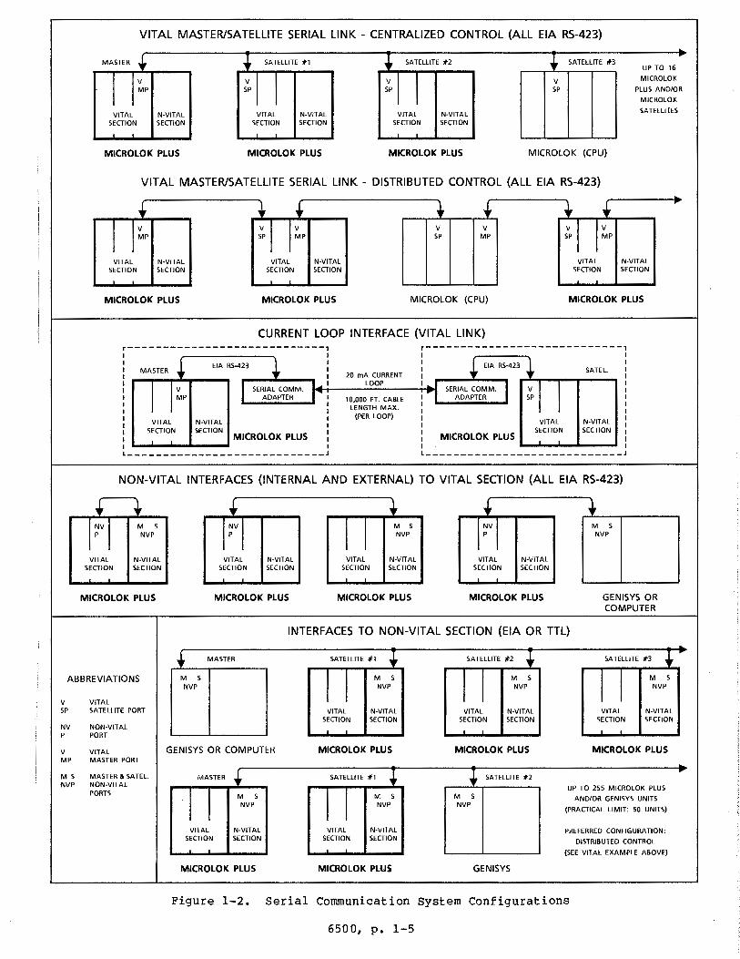
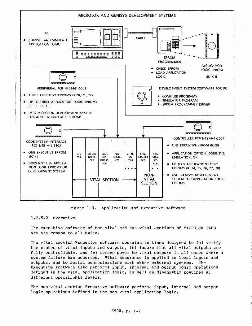
1.2.5 Executive and Application Software (See Figure 1-3)
Each section (vital and non-vital) of the MICROLOK PLUS unit incorporates its own, independent Application and Executive software. These are contained in EPROM chips on the logic boards of the respective sections.
1.2.5.1 Application
The Application software or logic in each section is developed for the specific installation, either by US&S or the customer. The source program is written and "compiled" on a computer, using a language that enables the system logic to be expressed in terms familiar to the railroad engineer. The finished program is converted into a form that can be entered or "burned" into the EPROM chips.
The MICROLOK PLUS vital application logic can be developed using the optional MICROLOK Development System (M.D.S.), which consists of a personal computer, EPROM programmer, EPROM eraser, and software program disks. This system allows the user to conduct all phases of application program development, including compilation on a personal computer, debugging, and final checking (simulation) and programming into the vital application logic EPROMs.
The non-vital application logic can be developed using the optional GENISYS Development System (G.D.S.). This system provides the same program development, testing and EPROM-loading features as the M.n.s., and uses the same programming and loading equipment. However, the G.D.S. uses different development software for its non-vital logic function.
6500, p. 1-6
MICROLOK AND GENISYS DEVELOPMENT SYSTEMS
PC
• COMPILE AND SIMULA TE APPLICATION LOGIC.
lliO[OOIJD=CABLE D -· (g)
I ~========= I - - -:
PERIPHERAL PCB N451441-5502
• THREE EXECUTIVE EPROMS (IC20, 21, 22)
• UP TO THREE APPLICATION LOGIC EPROMS (IC 15, 16, 19)
• USES MICROLOK DEVELOPMENT SYSTEM FOR APPLICATION LOGIC EPROMS
CODE SYSTEM INTERFACE PCB N451441-5302
• ONE EXECUTIVE EPROM (IC14)
• DOES NOT USE APPLICATION LOGIC EPROMS OR DEVELOPMENT SYSTEM
CPU PCB
1/0 BUS
INTERF.
PCB
•
CODE PERI· SYS. PHERAL
INTERF. PCB
PCB
VITAL SECTION
VITAL
110
PCBS
. . . . ~
~
EPROM PROGRAMMER
• CHECK EPROM
---
• LOAD APPLICATION LOGIC.
--- - - - "'---J""
APPLICATION LOGIC EPROM
BK X 8
DEVELOPMENT SYSTEM SOFTWARE FOR PC
• COMPILER PROGRAMS • SIMULATOR PROGRAM • EPROM PROGRAMMER DRIVER
CONTROLLER PCB N451441-5602
• ONE EXECUTIVE EPROM (IC29)
CON· NON· • APPLICATION OPTION: CODE SYS. TROLLER VITAL
PCB 110
PCBS
• • NONVITAL
SECTION
I
EMULATION, OR:
• UP TO 5 APPLICATION LOGIC EPROMS (IC 24, 25, 26, 27, 28)
• USES GENISYS DEVELOPMENT SYSTEM FOR APPLICATION LOGIC EPROMS
Figure 1-3. Application and Executive Software
1.2.5.2 Executive
The executive software of the vital and non-vital sections of MICROLOK PLUS are are common to all units.
The vital section Executive software contains routines designed to (a) verify the states of vital inputs and outputs, (b) insure that all vital outputs are fully controllable, and (c) remove power to vital outputs in all cases where a system failure has occurred. Vital assurance is applied to local inputs and outputs, and to serial communications with other external systems. The Executive software also performs input, internal and output logic operations defined in the vital application logic, as well as diagnostic routines at different operational levels.
The non-vital section Executive software performs input, internal and output logic operations defined in the non-vital application logic.
6500, p. 1-7
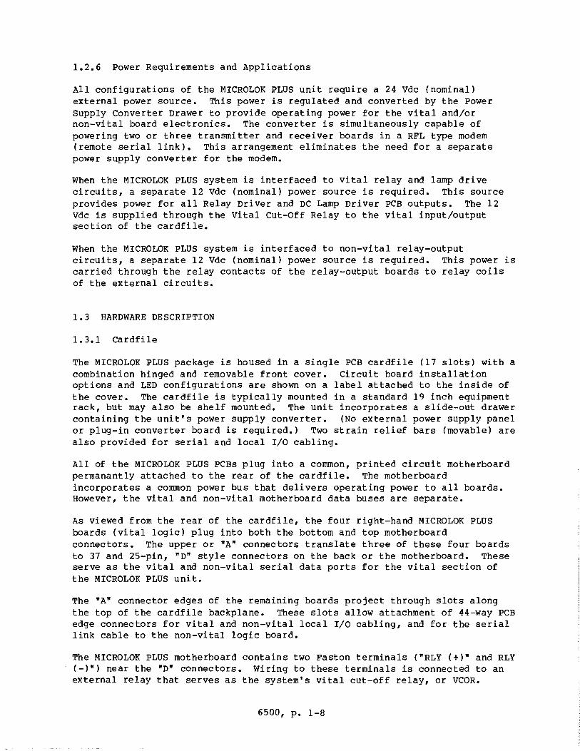
1.2.6 Power Requirements and Applications
All configurations of the MICROLOK PLUS unit require a 24 Vdc (nominal) external power source. This power is regulated and converted by the Power Supply Converter Drawer to provide operating power for the vital and/or non-vital board electronics. The converter is simultaneously capable of powering two or three transmitter and receiver boards in a RFL type modem (remote serial link). This arrangement eliminates the need for a separate power supply converter for the modem.
When the MICROLOK PLUS system is interfaced to vital relay and lamp drive circuits, a separate 12 Vdc (nominal) power source is required. This source provides power for all Relay Driver and DC Lamp Driver PCB outputs. The 12 Vdc is supplied through the Vital cut-Off Relay to the vital input/output section of the cardfile.
When the MICROLOK PLUS system is interfaced to non-vital relay-output circuits, a separate 12 Vdc (nominal) power source is required. This power is carried through the relay contacts of the relay-output boards to relay coils of the external circuits.
1.3 HARDWARE DESCRIPTION
1.3.1 Cardfile
The MICROLOK PLUS package is housed in a single PCB cardfile (17 slots) with a combination hinged and removable front cover. Circuit board installation options and LED configurations are shown on a label attached to the inside of the cover. The cardfile is typically mounted in a standard 19 inch equipment rack, but may also be shelf mounted. The unit incorporates a slide-out drawer containing the unit's power supply converter. (No external power supply panel or plug-in converter board is required.) Two strain relief bars (movable) are also provided for serial and local I/0 cabling.
All of the MICROLOK PLUS PCBs plug into a common, printed circuit motherboard permanantly attached to the rear of the cardfile. The motherboard incorporates a connnon power bus that delivers operating power to all boards. However, the vital and non-vital motherboard data buses are separate.
As viewed from the rear of the cardfile, the four right-hand MICROLOK PLUS boards (vital logic) plug into both the bottom and top motherboard connectors. The upper or "A" connectors translate three of these four boards to 37 and 25-pin, "D" style connectors on the back or the motherboard. These serve as the vital and non-vital serial data ports for the vital section of the MICROLOK PLUS unit.
The "A" connector edges of the remaining boards project through slots along the top of the cardfile backplane. These slots allow attachment of 44-way PCB edge connectors for vital and non-vital local I/0 cabling, and for the serial link cable to the non-vital logic board.
The MICROLOK PLUS motherboard contains two Faston terminals ("RLY (+)" and RLY (-)") near the "D" connectors. Wiring to these terminals is connected to an external relay that serves as the system's vital cut-off relay, or VCOR.
6500, p. 1-8
t"lj ..... LO s:: t'1 CD
..... I ~ . n $11 t'1 0. Hl ..... ..... CD
°' G) U1 CD 0 :::, 0 CD ... t'1
$11 'Cl ..... .
t1 ..... (1) I. C/l
"° .....
LO :::,
$11 :::, 0.
"d n tl1
> t'1 t'1 $11 :::,
LO CD :I CD :::, rt C/l
VITAL SECTION PCBS - CPU FRONT NON-VITAL SECTION PCB - LOGIC
SLOT PART NO. DESCRIPTION A B C D E F G H K L M N OPQ SLOT PART NO. DESCRIPTION A N451441·5701 PROCESSOR NON-VITAL SECTION 0 N451441·5602 CONTROLLER B N451441·6001 1/0 BUS INTERFACE
c N451441·5302 CODE SYSTEM INTERFACE D N451441·5502 PERIPHERAL
INSTALLATION
PROCESSOR SLOT A, ALL VITAL APPLICATIONS 110 BUS INTERFACE SLOT B, ALL VITAL APPLICATIONS CODE SYSTEM INTERFACE SLOT C, WHEN REQ'D BY APPLICATION PERIPHERAL SLOT D, ALL VITAL APPLICATIONS
J,T~L ~ 111 CPU
~-- ..... VITAL "W I I I
-.1 I I VITAL SECTION
INSTALLATION
SLOT 0, ALL NON-VITAL APPLICATIONS
NON-VITAL SECTION PCBS - 1/0
SLOT PART NO. DESCRIPTION
P, Q N451441·3601 CONTROL DEVLIVERYT N451441·7101 CONSTANT DELIVERY
VITAL SECTION PCBS - 1/0 N451441-4701 CONTROL & DELIVERY
N451441·7202 OPTO·INPUT (HIGH THRESHOLD)
SLOT PART NO. DESCRIPTION N451441·5802 OPTO·INPUT (WIDE RANGE)
f • N N451441·6501 STANDARD RELAY DRIVER INSTALLATION N451441·8601 STANDARD RELAY DRIVER W/LEDS ONE RELAY-OUTPUT: SLOT P N451441·7401 VOLT.·LIMIT. RELAY DRIVER ONE OPTO·INPUT: SLOT P N451441·8501 VOLT.·LIMIT. RELAY DRIVER W/LEDS ONE RELAY·OUTPUT AND ONE OPTO·INPUT: N451441·6601 Bl·POLAR RELAY DRIVER RELAY IN SLOT P, OPTO IN SLOT Q N451441·8701 Bl·POLAR RELAY DRIVER W/LEDS N451441·6702 DC LAMP DRIVER, 18 W LAMP N451441·6703 DC LAMP DRIVER, 25 W LAMP N451441·7301 DC LAMP DRIVER, 36 W LAMP N451441·6402 STANDARD INPUT, 12 V NOM.
+12V ·12V +SV ·SV 24V OUTPUT OUTPUT OUTPUT OUTPUT INPUT
44·WAY PCB VITAL CODE VITAL
LED LED LED LED LED EDGE CONNECTORS MASTER SYSTEM SLAVE
(VITAL 1/0 AND PORT PORT PORT N451441 ·6403 STANDARD INPUT, 24 V NOM. N451441 ·8802 STANDARD INPUT, 12 V NOM., W/LEDS
POWER SUPPLY DRAWER ALL NON-VITAL PCBS) 37·PIN "D" 25·PIN "D" 37·PIN "D"
N451441·8803 STANDARD INPUT, 24 V NOM, W/LEDS
INSTALLATION: SEE EXAMPLES BELOW
CARD SLOT ID --+- 0 P Q N M
VITAL 1/0 INSTALLATION EXAMPLES
EXAMPLE: 6 OUTPUT PCBS ONLY
I I I 1::: ' ' I ~1111
VITAL 1/0 "ft: j j j I I I I I I I I I I I I I I I I
I I I
L 1 ST OUTPUT PCB IN SLOT E
'--y-)
t NO EMPTY SLOTS
BETWEEN PCBS
EXAMPLE: 5 INPUT PCBS ONLY
I I I ! ! ! I VITAL 1/0 "ft: j j j
I I I I I I I I I I I I I I I I I I I I I I I I I I I
1 ST INPUT PCB IN SLOT E
'--y-)
t NO EMPTY SLOTS
BETWEEN PCBS
EXAMPLE: 4 OUTPUT PCBS 3 INPUT PCBS
I II I I ! I VITAL 1/0 "ft: j j j
I I I I I I I I I
1ST INPUT PCB IN SLOT I
1ST OUTPUT PCB IN SLOT E
~
NO EMPTY SLOTS BETWEEN PCBS
MOTHERBOARD (COVER OFF)
24 V INPUT TERMINALS
REAR
VCOR OUTPUT TERMINALS
1.3.2 Plug-In Printed Circuit Boards
1.3.2.1 General Arrangement
A. Vital Section
Slots A through D of the MICROLOK PLUS cardfile contain the vital section logic or "CPU".
a. All MICROLOK PLUS units used for vital control applications are always equipped with a Processor PCB in slot A and a Peripheral PCB in slot D.
b. When the unit is connected to another vital controller (MICROLOK PLUS or MICROLOK) through a serial data link, or local vital inputs/outputs are required, an I/0 Bus Interface PCB is installed in slot B.
c. When the unit is connected to an external non-vital controller (GENISYS) or cross-connected to its own non-vital section, a Code System Interface PCB is installed in slot c.
When the MICROLOK PLUS system is interfaced to vital local circuits, various arrangements of vital-output (relay-driver, lamp-driver) and vital-input boards are installed in slots E through N, according to the application.
a. When the application requires relay and/or lamp driver boards only, these are always installed starting in slot E.
b. When the application requires vital input boards only, these are also installed starting in slot E.
c. When the application requires both vital output (relay and/or lamp driver) and vital input boards, the output boards are always installed starting in slot E. The first input board is installed after the last output board.
d. No empty slots are permitted between vital output and input boards.
B. Non-Vital Section
Slots O through Q contain the MICROLOK PLUS non-vital section boards.
All MICROLOK PLUS units used for non-vital control functions are equipped with a Controller PCB in slot o.
When the MICROLOK PLUS unit is interfaced to non-vital local circuits, different combinations of non-vital relay-output and optical-input boards are installed in slots P and Q, according to the application.
a. When the application requires only one relay-output or optical-input board, this board is always installed in slot P.
b. When the application requires one relay-output and optical-input board, the relay-output board is always installed in slot P and the optical-input board is always installed in slot Q.
6500, p. 1-10
1.3.2.2 Vital CPU PCBs
The MICROLOK PLUS vital section uses the same Vital CPU boards as the MICROLOK system. For general descriptions of these boards, refer to:
Subject Cross Reference
Processor PCB (N451441-5701) SM-6400C, section 3.3.8.1, page 3-57
Peripheral PCB (N451441-5502) SM-6400C, section 3.3.8.2, page 3-60
NOTE
The Failover circuitry and LOCK-ON/AUTO/LOCK OFF switch on the Peripheral PCB are not used in the MICROLOK PLUS unit.
I/0 Bus Interface PCB (N451441-6001)
Code System Interface PCB (N451441-5302)
1.3.2.3 Vital I/0 PCBs
SM-6400C, section 3.3.8.3, page 3-64
SM-6400C, section 3.3.8.4, page 3-67
The MICROLOK PLUS vital section uses the same Vital I/0 boards as the MICROLOK system. For general descriptions of these boards, refer to:
Subject Cross Reference
Standard Relay Driver PCBs (N451441-6501 and -8601)
SM-6400C, section 3.3.8.5, page 3-72
Voltage-Limited Relay Driver (PCBs N451441-7401 and -8501)
SM-6400C, section 3.3.8.5, page 3-72
Bipolar Relay Driver PCBs (N451441-6601 and -8701)
SM-6400C, section 3.3.8.6, page 3-75
DC Lamp Driver PCBs (N451441-6702, -6703 and -7301)
SM-6400C, section 3.3.8.7, page 3-78
Standard Input PCBs SM-6400C, section 3.3.8.8, page 3-85 (N451441-6402, -6403, -8802, -8803)
The May 1987 (revised March, 1989) edition of SM-6400C only describes the following vital I/0 boards:
Standard Relay Driver Voltage-Limited Relay Driver Bipolar Relay Driver Standard Input Standard Input
6500, p. 1-11
US&S Part No.
N451441-6501 N451441-7401 N451441-6601 N451441-6402 N451441-6403
Both MICROLOK and MICROLOK PLUS also use new vital I/0 boards equipped with LEDs on the individual input or output lines. These boards are as follows:
US&S Part No.
Standard Relay Driver Voltage-Limited Relay Driver Bipolar Relay Driver Standard Input
N451441-8601 N451441-8501 N451441-8701 N451441-8802 N451441-8803 Standard Input
The descriptions of the vital I/0 boards in sections 3.3.8.5, 3.3.8.6 and 3.3.8.8 of SM-6400C are applicable to the above boards, except that no reference is made to LEDs on the I/0 lines.
1.3.2.4 Non-Vital Controller PCB
The MICROLOK PLUS non-vital section uses the same Controller PCB as the GENISYS system. For a general description of this board, refer to:
Subject Cross Reference
Controller PCB (N451441-5602) SM-6300C, section 1.2.2.1, page 1-4
1.3.2.5 Non-Vital I/0 PCBs
The MICROLOK PLUS non-vital section uses the same non-vital I/0 PCBs GENISYS system. For general descriptions of these boards, refer to:
Subject
Constant Delivery PCB (N451441-7101)
Control Delivery PCB (N451441-3601)
Control and Delivery PCB (N451441-4701)
Optical-Input PCB - High Threshold Type (N451441-7202)
Optical-Input PCB - Wide Range Type (N451441-5802)
Cross Reference
SM-6300C, section 1.2.2.2, page 1-5
SM-6300C, section 1.2.2.2, page 1-5
SM-6300C, section 1.2.2.2, page 1-5
SM-6300C, section 1.2.2.3, page 1-6
SM-6300C, section 1.2.2.3, page 1-6
6500, p. 1-12
1.4 AUXILIARY EQUIPMENT
1.4.1 Vital Cut-Off Relay (VCOR)
The MICROLOK PLUS system requires an external vital relay to serve as the cut-off mechanism for its vital outputs. This relay is controlled by the vital section microprocessor (Processor PCB) and is operated by a separate driver circuit on the I/0 Bus Interface PCB. A US&S PN-150HD relay is used for this purpose. For a general description of this relay, refer to:
Subject
Vital Cut-Off Relay (VCOR) PN-150HD (N322505-701)
Cross Reference
SM-6400B, section 1.2.2.4, page 1-9
1.4.2 Serial Communications Adapter Panel N451460-3001
When the MICROLOK PLUS application requires a 20 mA Current Loop communications link to another controller (i.e. in separate wayside houses), the system is augmented with the Serial Communications Adapter Panel.
For a general description of the Serial Communications Adapter Panel, refer to:
Subject
Serial Communications Adapter Panel (N451460-3001)
Cross Reference
SM-6400B, section 1.2.2.5, page 1-10
NOTE
When used with MICROLOK PLUS, the Serial Communications adapter panel requires a separate external power source.
1.5 SPECIFICATIONS
1.5.1 Physical/Mechanical
Cardfile Dimensions:
Cardfile Mounting:
Cardfile Access:
Standard 19" rack or shelf
To plug-in PCBs: Hinged/removable front cover.
To power supply converter: Slide-out drawer.
To motherboard PCB backplane connectors and jumpers: Removable cover.
6500, p. 1-13
External Connections:
1.5.2 Electrical
1.5.2.1 Power Supply Converter
Power Input:
Power Supply Output:
Fuse:
Overvoltage Protection:
Common Mode Filtering:
Differential Mode Filtering:
Vital Section/CPU:
Two 37-pin "D" connectors, female (vital Master and Satellite ports)
One 25-pin "D" connector, female (vital interface to non-vital controller for EIA/code system interface)
Vital Section I/0:
Slots for up to ten 44-pin PCB edge connectors (vital local input and local output drive)
Non-Vital Section (Controller and I/0)
Slots for up to three 44-pin PCB edge connectors (serial and local I/0)
Power Supply Converter (Drawer)
Two dual-Faston terminals (male) for 24 Vdc power input.
One AAR stud on rear of cardfile (for earth ground)
19.8 to 32.4 Vdc (24 Vdc nom.)
120 Vac input, externally converted to 24 Vdc output@ 7 amps
24 Vdc external battery source@ 7 amp/hr.
12 Vdc available for RFL modem 270 mA on +12 Vdc 135 mA on -12 Vdc
Fuse: 6.25 amp, 250 Vdc, 3 AG style
Transzorb on input, overvoltage clamping on +5V output
Provided on power input and outputs
Provided on power input
6500, p. 1-14
Power Converter Characteristics:
1.5.2.2 Vital I/0 PCBs
Isolation (input to output): 500V Isolation (terminal to case): 500V Switching frequency: 200 kHz, typ. Efficiency: 80%, typ. Fault protection: Reverse polarity, overvoltage (clamping) main, short circuit (indefinite, autorecovery)
The MICROLOK PLUS vital section uses the same vital I/0 PCBs as MICROLOK. For electrical specifications on these PCBs, refer to:
Subject
Standard, Voltage-Limited and Bipolar Relay Driver PCBs -Specifications
DC Lamp Driver PCB -Specifications
1.5.2.3 Non-Vital I/0 PCBs
Cross Reference
SM-6400B, section 2.8.2.1, page 2-21
SM-6400B, section 2.8.2.2, page 2-25
The MICROLOK PLUS non-vital section uses the same non-vital I/0 PCBs as GENISYS. For electrical specifications on these PCBs, refer to the following:
Subject
Control Delivery, Constant Delivery, Control and Delivery PCBs - Specifications
Optical-Input PCBs -Specifications
1.5.3 Environmental
Temperature Range:
Cardfile Cooling:
1.5.4 Miscellaneous
Vital Section CPU Capacity:
Vital Section I/0 Capacity:
Cross Reference
SM-6300B, section 1.3.2.3, page 1-7
SM-6300B, section 1.3.2.4, page 1-7
-400 to +7o0c@ 90% noncondensing humidity
Convection through louvers
Up to four PCBs (application dependent)
Up to 10 PCBs (application dependent)
6500, p. 1-15
Non-Vital Section Capacity:
Master/Satellite System Capacities:
Up to three PCBs (application dependent)
Vital section: Up to 16 MICROLOK PLUS or MICROLOK Satellite units on Master port.
Non-Vital Section: Up to 255 MICROLOK PLUS or GENISYS units on Controller PCB Master port. Practical limit: 50 Satellite units.
Serial Comm. Modes, Vital Section: - Vital Master and Satellite Ports:
Serial Comm. Modes, Non-Vital Section:
Serial Interfaces, Vital Section:
Serial Interfaces, Non-Vital Section:
Serial Bit Rates, Vital Section:
Full duplex (standard)
Data Security: BCH, 24 Bits
Non-Vital Port: Half or full duplex
Half or full duplex
Vital Master and Satellite Ports:
EIA RS-423, RS-232C compatible
Optional: 20 mA current loop (EIA converted at optional Serial Communications Adapter)
Non-Vital Port: EIA RS-423, RS-232C compatible
EIA RS-423, RS-232C compatible
Optional: 20 mA current loop (EIA converted at optional Serial Communications Adapter)
Vital Master and Satellite Ports:
EIA: 150, 300, 600, 1200, 1800, or 2400
20 mA current loop: Distance d~e~e~
Non-Vital Port:
EIA: 50, 75, 110, 134, 150, 300, 600, 1200, 1800, 2400, 3600, 4800, 7200 or 9600
20 mA current loop: Distance dependent
6500, p. 1-16
Serial Bit Rates, Non-Vital
current Loop Total Cable Length:
Maintenance Aids:
Top Part Numbers:
Cardfile w/P. s. and Cable Cardfile wo/P. s. P. s. Drawer Power Input Cable
Vital Section:
Processor PCB I/0 BUS Interface PCB Code System Interface PCB Peripheral PCB
Standard Input (wo/LEDs) Standard Input (wo/LEDs) Standard Input (w/LEDs) Standard Input (w/LEDs) standard Relay Driver (wo/LEDs) Standard Relay Driver (w/LEDs) Volt.-Ltd. Relay Driver (wo/LEDs) Volt.-Ltd. Relay Driver (w/LEDs) Bipolar Relay Driver (wo/LEDs) Bipolar Relay Driver Cw/LEDs) DC Lamp Driver DC Lamp Driver DC Lamp Driver
Non-Vital Section:
Controller Control Delivery Constant Delivery Control and Delivery Indication Opto (High Threshold) Indication Opto (Wide Range)
EIA: 50, 75, 110, 134, 150, 300, 600, 1200, 1800, 2400, 3600, 4800, 7200 or 9600
20 mA current loop: Distance dependent
10,000 feet (max.)
Plug-In PCBs (for PCB swapping) Diagnostic/Status LEDs PCB test points IC plug-in sockets (for res with 24 or more pins)
- N451796-0102 N451796-0101 N451796-0301 N451795-1401
N451441-5701 N451441-6001 N451441-5302 N451441-5502
N451441-6402 (12 V nom. input) N451441-6403 (24 V nom. input) N451441-8802 (12 V nom. input) N451441-8803 (24 V nom. input) N451441-6501
- N451441-8601 N451441-7401 N451441-8501 N451441-6601 N451441-8701 N451441-6702 (18 W lamp) N451441-6703 (25 w lamp) N451441-7301 (36 w lamp)
N451441-5602 - N451441-3601 - N451441-7101
N451441-4701 N451441-7202 N451441-5802
6500, p. 1-17
Misc.
Serial Communications Adapter PN-150HD Relay (VCOR) Application Logic Blank EPROM* Serial Link Cables
N451460-3001 N322505-701 J715029-0409 (Refer to section A.3.1)
*Used for both Vital and Non-Vital section application logic
6500, p. 1-18
2.1 SHIPMENT HANDLING
SECTION II INSTALLATION
The MICROLOK PLUS cardfile is shipped without plug-in PCBs. These PCBs are delivered in separate packages, with types and quantities determined by the application. If storing MICROLOK PLUS equipment for an extended period prior to installation, make certain storage area temperatures keep within the range of -40 to +as0 c. If any equipment is damaged in shipping, do not attempt to make repairs. Such equipment should be returned to US&S for repair or replacement.
For testing of newly received or stored MICROLOK PLUS hardware, refer to:
Subject Cross Reference
Equipment Retesting Guidelines SM-6400C, section 3.4, page 3-108
2.2 UNIT MOUNTING AND ENVIRONMENT
The MICROLOK PLUS cardfile is designed for mounting in a standard 19 inch equipment rack. The unit may also be shelf-mounted.
Environmental requirements for the MICROLOK PLUS unit are the same as those for the MICROLOK rack. For environmental recommendations, refer to:
Subject Cross Reference
Equipment Environment SM-64008, section 2.2, page 2-1
2.3 FACILITY WIRING
Facility wiring practices for the MICROLOK PLUS unit are the same as those for the MICROLOK system. For circuit practices, refer to:
Subject Cross Reference
Facility Wiring Practices SM-64008, section 2.3, page 2-2
6500, p. 2-1
PO:;;T~N:UT { 824-1 #10 t4
TERMINALS 824 ON
POWER SUPPLY If DRAWER
(CARDFILE N24-I #10 ELECTRONICS) a,-----------,.==::::::ir------°', 1:,,..,.-•3
824
.,,, N
24 TRANSZORBS (QTY = 2) i'
N24
VCOR ~--_.___..--_- - - - - , I 812-2
812-ZA
7(
N12-2
N12-2A
TO VITAL 1/0 WIRING ONLY
812~3
B12-3A
N12-3
N12-3A
NON-VITAL SECTION
_j_ TO EARTH GROUND
® TWISTED PAIR WIRES
4 e TERMINAL STRIP
~ '11 : CONNECTOR STRAP
ALL WIRING #12 UNLESS OTHERWISE INDICATED
PROVIDE SEPARATE B TERMINAL FOR EACH
VITAL OUTPUT. STRAP TOGETHER
PROVIDE SEPARATE N TERMINAL FOR EACH
VITAL OUTPUT. STRAP TOGETHER
NON-VITAL OUTPUT RELAY
TYPE 5KP40A
II
US&S PART NO. J792736-0036
#10
0.1 to 0.15 mFd 50V(HIQ)
#10 ,:.,"
TRANSZORBS (QTY = 2) TYPE 5KP16A
.,, ,
US&S PART NO. J792736-0030
W:---
#6 812
3 #6 N12
KEEP WIRE RUNS FROM BATTERY TO USSP AND FROM USSP TO MICROLOK PLUS TERMINAL STRIP AS SHORT AS POSSIBLE.
z
44-WAY CONN.
y
STANDARD RELAY DRIVER VOL T.-LIMIT. RELAY DRIVER Bl-POLAR RELAY DRIVER DC LAMP DRIVER
~---1-----;.._ ___ _:...,, •4.;----
II
W:---
""'
21 I
I 4 L-------...l
STANDARD MICROLOK 1/0 CABLES
4
#14
#14 3
USSP-11 32 VD( 15 AMP
N451552-0515
VITAL SECTION
#10 824
#10 N24
n ~'------·--------'(4: ON-BOARD RELAY M - 1FORBCONTACT II
W:::::a
II
W:::::a
REFER TO SECTION 2.10
FOR BOARD APPLICA·
44-WAY CONN.
1..-------STANDARD GENISYS 1/0 CABLES
I I
: CONTROL DELIVERY I CONSTANT DELIVERY : CONTROL & DEVLIVERY I I ON-BOARD RELAY
: HEEL
L--------
Figure 2-1. Typical MICROLOK PLUS Power Input Wiring
6500, p. 2-3
2.4 POWER AND GROUND CIRCUITS
2.4.1 Power Sources
The MICROLOK PLUS system requires a single 24 Vdc source for operating power. Basic power specifications are the same as those for the MICROLOK system. For power input specifications, refer to:
S~j&t Cross Reference
Power source Specifications SM-6400B, section 2.4.1, page 2-2
NOTES
The input voltage range for the MICROLOK PLUS power supply converter is 19.8 to 32.4 Vdc, 24 Vdc nominal.
SM-6400B, section 2.4.1, page 2-2: The vital I/0 power requirements described in this section are applicable to the vital section of the MICROLOK PLUS unit.
When the non-vital section of MICROLOK PLUS is interfaced to local relay I/0 circuits, a separate 12 Vdc power source is required to energize individual inputs and outputs. If the vital section includes local relay and/or lamp driver outputs, the 12 Vdc power bus for these outputs can also be used to power the non-vital relay circuits. Make certain to wire the non-vital relay load according to Figure 2-1 of SM-6400B (as "OTHER LOAD").
2.4.2 Wiring and Surge/Noise Protection
Wiring and surge/noise recommendations for the MICROLOK PLUS unit are the same as those for the MICROLOK system. For these recommendations, refer to:
Subject
Wiring and Surge/Noise Protection
Cross Reference
SM-6400B, section 2.4.2, pages 2-3 through 2-5
NOTES
Section 2.4.2.2, part c, Note 3: The MICROLOK PLUS 24 Vdc power input does not require a HI-Q filtering capacitor.
Figure 2-1 on the following page is a typical power input wiring schematic for the complete MICROLOK PLUS system. Refer to this figure in place of Figure 2-2 of the MICROLOK manual SM-6400B.
6500, p. 2-2
2.4.3 Equipment Grounding (See Figure 2-2)
2.4.3.1 Rack and Cardfile Grounding
When the MICROLOK PLUS unit is installed in an equipment rack (rather than shelf mounted), rack grounding requirements are the same as those for the MICROLOK system. For these requirements, refer to:
S~j&t Cross Reference
Equipment Rack Grounding SM-6400B, section 2.4.3.1, page 2-6
NOTES
The MICROLOK PLUS cardfile is equipped with a single AAR stud for chassis grounding to the equipment rack. Run a minimum of #6 wire from the stud to the rack prime ground stud. Keep this wire as short as possible.
2.4.3.2 0 Volts Connection to Earth Ground
MICROLOK PLUS does not require an AC ground (0 volts connection to earth ground through capacitor) for noise protection; this is provided internally.
However, if the unit is used with a Serial Communications Adapter Panel or vital serial link modem, 0 volts on these units should be connected together and run to the rack prime ground stud through a 0.1 to 0.15 mFd, 200 volt (or greater) capacitor. Acceptable types of capacitors include polystyrene, polypropylene, polycarbonate or metalized polyester (Mylar). When the installation is complete, check the O volts to make sure it is still electrically isolated from the prime ground.
2.4.3.3 Serial and Local Cable Connection to Earth Ground
Each of the MICROLOK PLUS vital section serial communications cables (Master, Satellite and non-vital link) must be shielded. Connect the shields on these cables to earth ground on one end only. For vital serial interface cable schematics, refer to:
Subject
Vital Serial Cable Schematics
Cross Reference
SM-6400B, section 2.9.4, pages 2-46 through 2-59
NOTE
The redundant-CPU schematics in this section are not applicable to the MICROLOK PLUS system.
6500, p. 2-4
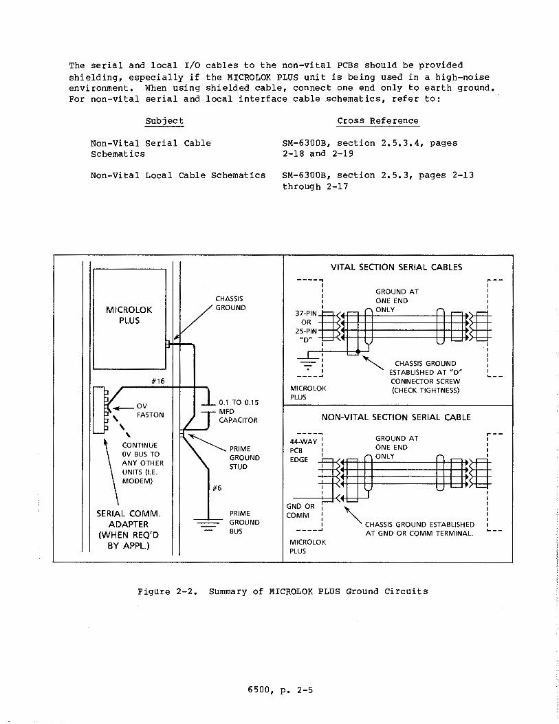
The serial and local I/0 cables to the non-vital PCBs should be provided shielding, especially if the MICROLOK PLUS unit is being used in a high-noise environment. When using shielded cable, connect one end only to earth ground. For non-vital serial and local interface cable schematics, refer to:
Subject Cross Reference
Non-Vital Serial Cable Schematics
Non-Vital Local Cable Schematics
MICRO LOK PLUS
#16
.......-ov ' FAS TON
' " CONTINUE OV BUS TO ANY OTHER UNITS (I.E. MODEM)
SERIAL COMM. ADAPTER
(WHEN REQ'D BY APPL.)
CHASSIS GROUND
0.1 TO 0.15 MFD CAPACITOR
#6
PRIME GROUND BUS
SM-63008, section 2.5.3.4, pages 2-18 and 2-19
SM-63008, section 2.5.3, pages 2-13 through 2-1 7
VITAL SECTION SERIAL CABLES
----~ ~--I I I GROUND AT I I I I ONE END I I I
3~;1Ni ONLY ~ 25-PIN 4+-t-+-1-------+-+-+--++
"D" I I
____ .... MICROLOK PLUS
CHASSIS GROUND ESTABLISHED AT "D" CONNECTOR SCREW (CHECK TIGHTNESS)
NON-VITAL SECTION SERIAL CABLE
----~ 44_WAY : GROUND AT
I I I I I
I I I ::l!D ~g~~v'ND ~ms I I I I I
GND OR 1 '
COMM : "' I CHASSIS GROUND ESTABLISHED
____ ..., AT GND OR COMM TERMINAL.
MICROLOK PLUS
I I ,... __
Figure 2-2. Summary of MICROLOK PLUS Ground Circuits
6500, p. 2-5
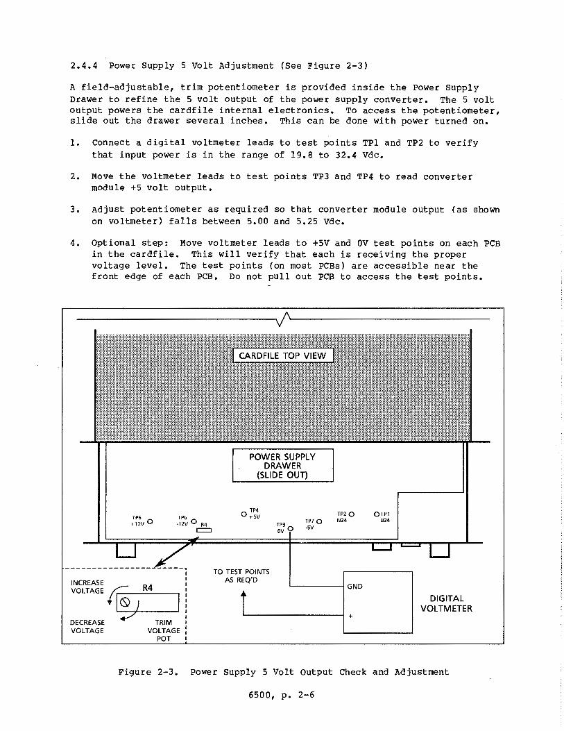
2.4.4 Power Supply 5 Volt Adjustment (See Figure 2-3)
A field-adjustable, trim potentiometer is provided inside the Power supply Drawer to refine the 5 volt output of the power supply converter. The 5 volt output powers the cardfile internal electronics. To access the potentiometer, slide out the drawer several inches. This can be done with power turned on.
1. Connect a digital voltmeter leads to test points TPl and TP2 to verify that input power is in the range of 19.8 to 32.4 Vdc.
2. Move the voltmeter leads to test points TP3 and TP4 to read converter module +5 volt output.
3. Adjust potentiometer as required so that converter module output (as shown on voltmeter) falls between 5.00 and 5.25 Vdc.
4. Optional step: Move voltmeter leads to +5V and OV test points on each PCB in the cardfile. This will verify that each is receiving the proper voltage level. The test points (on most PCBs) are accessible near the front edge of each PCB. Do not pull out PCB to access the test points.
TP6 ·12V O R4
[:=:::J
INCREASE R4
VOLTAGE C----~ •101
DECREASE ;_;, VOLTAGE
TRIM VOLTAGE
POT
POWER SUPPLY DRAWER
(SLIDE OUT)
Q TP4 +5V
TO TEST POINTS AS REQ'D
TP3Q ov
TP7 0 ·5V
TP2 0 N24
'-------1GND
~--------~ +
QTP1 824
DIGITAL VOLTMETER
Figure 2-3. Power supply 5 Volt output Check and Adjustment
6500, p. 2-6
2.4.5 Auxiliary Power for RFL Modem
MICROLOK PLUS is capable of powering two or three transmitter and receiver boards in an RFL modem used in the vital and/or non-vital serial link(s). This eliminates the need for a separate power connection and converter board in the modem. Auxiliary power from MICROLOK PLUS is provided through Faston terminals on the Power Supply. Output specifications are: 270 mA on +12 Vdc, 135 mA on -12 Vdc. This power source may also be used to operate other types of modems and devices used in conjunction with the MICROLOK PLUS non-vital serial interface; contact US&S for addition information.
2.5 PCB PREPARATION
2.5.1 Vital CPU
MICROLOK PLUS uses the same vital CPU boards as MICROLOK. For vital CPU board set-up procedures, refer to the following:
Subject
Peripheral PCB (N451441-5502) Switch/Jumper Set-Up
Cross Reference
SM-6400B, section 2.5.1.1, page 2-10
NOTE
The LOCK ON/AUTO/LOCK OFF switch (SW5) on the Peripheral PCB is not used in MICROLOK PLUS. However, always keep this switch in the AUTO position. If the LOCK LED is on, SW5 is not in the required AUTO position.
Peripheral PCB (N451441-5502) EPROM Installation
Code System Interface PCB (N451441-5302) Switch/Jumper Set-Up
SM-6400B, section 2.5.1.2, page 2-12
SM-6400B, section 2.5.1.3, page 2-13
The Processor and I/0 Bus Interface PCBs do not require any adjustments prior to installation in the MICROLOK PLUS cardfile.
2.5.2 Vital I/0
None of the vital input or output PCBs used in the MICROLOK PLUS cardfile requires any adjustments prior to installation.
6500, p. 2-7
2.5.3 Non-Vital Controller
MICROLOK PLUS uses the same non-vital Controller PCB as GENISYS. For set-up of the Controller PCB, refer to the following:
Subject
Controller PCB (N451441-5602) EPROM Installation
Controller PCB (N451441-5602) Switch/Jumper Set-Up
Cross Reference
SM-6300B, section 2.2.1, page 2-1
SM-6300B, sections 2.2.2 through 2.2.9, pages 2-1 through 2-6.
NOTE
Section 2.2.7: The EIA RS-423 mode is required when Controller PCB is interfaced with the vital section Code System port of the same MICROLOK PLUS unit.
2.5.4 Non-Vital I/0 PCBs
None of the MICROLOK PLUS non-vital section optical-input or relay-output PCBs require any adjustments prior to installation.
2.6 PCB INSTALLATION
Install the MICROLOK PLUS vital and non-vital PCBs as required by the the application and according to the guidelines in section 1.2.2.1 and Figure 1-4.
CAUTION
DO NOT INSTALL OR REMOVE ANY MICROLOK PLUS PLUG-IN PCBS WITH POWER TURNED ON, OTHERWISE FAULTY SYSTEM OPERATION AND/OR COMPONENT DAMAGE MAY RESULT.
For testing of the MICROLOK PLUS vital section PCBs prior to installation, refer to the following:
Subject Cross Reference
Equipment Retesting Guidelines SM-6400C, section 3.4, page 3-108
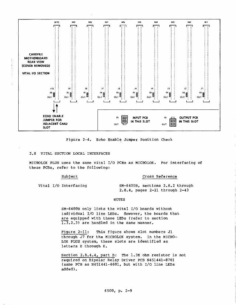
2.7 ECHO ENABLE JUMPERS (VITAL I/0)
Each vital I/0 card slot location that contains a PCB must be equipped with a blue Echo Enable Jumper on the cardfile back panel. These are installed at the factory per the application, but should be checked prior to putting the MICROLOK PLUS unit into service. As shown in Figure 2-4, place each jumper in the "INw position when a Standard Input board is installed in the corresponding card slot. Place the jumper in the "OUT" position when the card slot contains a standard Relay Driver, Voltage-Limited Relay Driver, Bipolar Relay Driver or DC Lamp Driver PCB.
6500, p. 2-8
M10 M9 MS M7 M6 MS M4 M3 M2 Ml
r:-:, r:-:, r:-:, r:-:, r:-:, r:-:, r:-:, r:-:, r:-:, r:-:,
CARDFILE MOTHERBOARD
REAR VIEW {COVER REMOVED)
VITAL 1/0 SECTION
J10: J9 : JS: J7 : J6 : JS : J4: J3 : J2: J1
IN :
OUT §1 IN :
OUT §1 IN 8: IN :
OUT §1 IN :
OUT §1 IN :
OUT §1 IN :
OUT §1 IN :
OUT §i IN :
OUT §i IN :
OUT ~i OUT C;
L_J L-...J L_J L_J L_J L_J L_J L-...J L-...J
it ECHO ENABLE IN INPUT PCB IN OUTPUT PCB JUMPER FOR I IN THIS SLOT I IN THIS SLOT . ADJACENT CARD OUT OUT
SLOT
Figure 2-4. Echo Enable Jumper Position Check
2.8 VITAL SECTION LOCAL INTERFACES
MICROLOK PLUS uses the same vital I/0 PCBs as MICROLOK. For interfacing of these PCBs, refer to the following:
Subject
Vital I/0 Interfacing
Cross Reference
SM-6400B, sections 2.8.2 through 2.8.4, pages 2-21 through 2-43
NOTES
SM-6400B only lists the vital I/0 boards without individual I/0 line LEDs. However, the boards that are equipped with these LEDs (refer to section 1.3.2.3) are handled in the same manner.
Figure 2-11: This figure shows slot numbers Jl through J7 for the MICROLOK system. In the MICROLOK PLUS system, these slots are identified as letters E through K.
Section 2.8.4.4, part D: The l.3K ohm resistor is not required on Bipolar Relay Driver PCB N451441-8701 (same PCB as N451441-6601, but with I/0 line LEDs added).
6500, p. 2-9
L_J
2.9 VITAL SECTION SERIAL INTERFACES
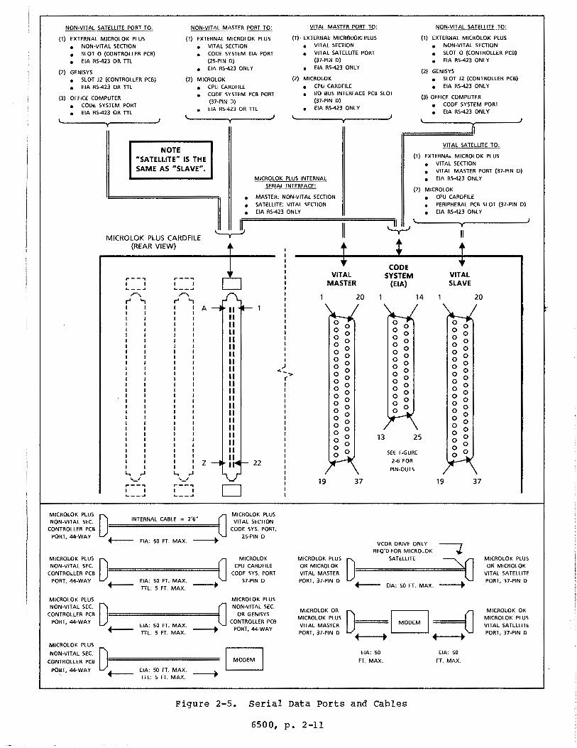
2.9.1 Serial Ports (See Figure 2-5)
When the vital section of MICROLOK PLUS is configured for serial communications with another vital control system (another MICROLOK PLUS or MICROLOK), cable connections are made on either or both of the two 37-pin "D" connectors (female) on the right hand side (rear view) of the cardfile. This can include EIA signal cables that go directly to another system or modem, or EIA cables that go to an external serial communications Adapter Panel for conversion to 20 mA current loop mode.
When the vital section of MICROLOK PLUS is also configured for non-vital serial communications with the non-vital section or an external GENISYS system, the external cable connection is made on the single 25-pin "D" connector located between the two 37-pin "D" connectors. The 25-pin connector is the external interface for the Code System PCB, and is hardwired to only support EIA communications.
When the unit's vital section is linked to the non-vital section, a serial data cable is run between the vital section 25-pin "D" connector and the 44-pin PCB edge connector on the non-vital Controller PCB. This particular link can only be configured for EIA communications, even though the Controller PCB has jumpers that also allow TTL communications.
2.9.2 Cabling General Notes
US&S provides standard cables for the following serial data interfaces from the MICROLOK PLUS vital section:
Link Type Mode
MICROLOK PLUS-to-MICROLOK PLUS Vital EIA*** MICRO LOK PLUS-to-MICRO LOK Vital EIA*** MICROLOK PLUS-to-MICROLOK PLUS* Non-Vital EIA only MICRO LOK PLUS-to-GEN I SYS Non-Vital EIA only MICROLOK PLUS Internal** Non-Vital EIA only
* From Code System port (vital section) of one MICROLOK PLUS to Controller PCB Port (non-vital section) of other MICROLOK PLUS.
** Vital section (Code System Interface PCB) to non-vital section (Controller PCB).
*** Can be converted to 20 mA current loop communications via Serial Communications Adapter Panel.
Two basic types of EIA cables are available; those that allow direct connection of two or more units, and those which interface MICROLOK PLUS to a serial data modem. US&S recommends these cables be used for all vital and non-vital serial links from the MICROLOK PLUS vital section.
6500, p. 2-10
NON-VITAL SATELLITE PORT TO: NON-VITAL MASTER PORT TO: VITAL MASTER PORT TO: NON-VITAL SATELLITE TO:
(1) EXTERNAL MJCROLOK PLUS (1) EXTERNAL MICROLOK PLUS (T) EXTERNAb MICROLO~ PLUS (1) EXTERNAL MICROLOK PLUS
• NON-VITAL SECTION • VITAL SECTION • VITAL SECTION • NON-VITAL SECTION
• SLOT O (CONTROLLER PCB) • CODE SYSTEM EIA PORT • VITAL SATELLITE PORT • SLOT O (CONTROLLER PCB)
• EIA RS-423 OR TIL (25-PIN D) (37-PIN D) • EIA RS-423 ONLY
(2) GENISYS • EIA RS-423 ONLY • EIA RS-423 ONLY (21 GENISYS
• SLOT J2 (CONTROLLER PCB) (2) MICROLOK (2) MICROLOK • SLOT J2 (CONTROLLER PCB)
• EIA RS-423 OR TIL • CPU CARDFILE • CPU CARDFILE • EIA RS-423 ONLY
• CODE SYSTEM PCB PORT • 110 BUS INTERFACE PCB SLOT (3) OFFICE COMPUTER (3) OFFICE COMPUTER
(37-PIN DJ (37·PIN D)
• CODE SYSTEM PORT EIA RS-423 OR TIL EIA RS-423 ONLY • CODE SYSTEM PORT
• • EIA RS-423 ONLY • EIA RS-423 OR TIL •
MICROLOK PLUS NON·VIT AL SEC.
CONTROLLER PCB PORT, 44-WAY
MICROLOK PLUS NON-VITAL SEC.
CONTROLLER PCB
PORT, 44·WAY
MICROLOK PLUS NON·VITAL SEC.
CONTROLLER PCB PORT, 44·WAY
MICROLOK PLUS
NON·VIT AL SEC.
CONTROLLER PCB
PORT, 44-WAY
NOTE "SATELLITE" IS THE SAME AS "SLAVE".
MICROLDK PLUS INTERNAL
SERIAL INTERFACE:
• MASTER: NON·VIT AL SECTION
• EIA RS-423 ONLY
VITAL SATELLITE TO:
(1) EXTERNAL MICROLOK PLUS
• VITAL SECTION • VITAL MASTER PORT (37-PIN D) • EIA RS-423 ONLY
(2) MICROLOK
• • •
CPU CARDFILE PERIPHERAL PCB SLOT (37-PIN D) EIA RS-423 ONLY
MICROLOK PLUS CARDFILE {REAR VIEW)
I a SATELLITE: VITAL SECTION
~·=,===========1=1 =====~'--~----v-11~~~-'
,..---. r---, I I I I
,,..., ,,..., r' .., r' .., I A II I I II I II I II
II II II II II II II II II
I II I II I II I I II I II I I II I II I II I z I 22 I
L, ,.J L, ,.J ... _/ ... _/
,----. ,..---, D I I I I
""--"" L.--.J
O INTERNAL CABLE 2'~ 0 +-- EIA: 50 FT. MAX. ~
MICROLOK PLUS VITAL SECTION
CODE SYS. PORT, 25·PIN D
EIA: 50 FT. MAX. TIL: 5 FT. MAX.
EIA: 50 FT. MAX. TIL: 5 FT. MAX.
EIA: 50 FT. MAX. TIL: 5 FT. MAX.
MICROLOK CPU CARDFILE
CODE SYS. PORT 37-PIN D
MICROLOK PLUS O NON-VITAL SEC. OR GENISYS
CONTROLLER PCB ---+ PORT, 44·WAY
"~.,,. (
CODE VITAL SYSTEM
MASTER (EIA}
20 14
0 0 0
0 0 0 0 0 0 0 0 0 0 0 0 0
0 0 0
0 0 0 0 0 0
0 0 0
0 0 0 0 0 0
0 0 0
0 0 0 0
0 0
0 13 25 0 0 0
0 0 SEE FIGURE
2·6 FOR
PIN·OUTS
19 37
MICROLOK PLUS OR MICROLOK VITAL MASTER PORT, 37-PIN D
MICROLOK OR MICROLOK PLUS VITAL MASTER PORT, 37-PIN D
VCOR DRIVE ONLY REQ'D FOR MICROLOK
EIA: 50
FT. MAX.
SATELLITE
EIA: 50 FT. MAX.
Figure 2-5. Serial Data Ports and Cables
6500, p. 2-11
VITAL SLAVE
0 0 0 0 0 0 0 0 0 0 0 0 0 0 0 0 0 0 0
19
EIA: 50
FT. MAX.
0 0 0 0 0 0 0 0 0 0 0 0 0 0 0 0 0 0
20
37
MICROLOK PLUS OR MICROLOK
VITAL SATELLITE
PORT, 37-PIN D
MICROLOK OR MICROLOK PLUS VITAL SATELLITE PORT, 37-PIN D
Direct-link EIA cables are available from US&S in various lengths up to 45 feet. Fifty feet is the US&S recommended maximum cable separation between two units in EIA communications. At greater lengths, line resistance and transient signals may cause interference with serial communications. A modem should be used when EIA cable length exceeds 50 feet, and/or the communications line leaves the equipment house containing the MICROLOK PLUS unit. MICROLOK PLUS-to-EIA modem cables are available in 20 foot lengths to allow cutting to the desired length.
2.9.3 Modem Recommendations
Consult US&S for recommendations on the modem used with MICROLOK PLUS vital and non-vital sections serial ports.
2.9.4 Vital Master and Satellite EIA Interfaces
For serial interfacing of the MICROLOK PLUS vital CPU, refer to the following:
Subject
Vital CPU Serial Interfacing
Cross Reference
SM-6400B, section 2.9.4, pages 2-46 through 2-55
NOTES
MICROLOK PLUS does not utilize redundant CPU serial interfaces. Ignore sections 2.9.4.2, 2.9.4.4, and 2.9.4.6 of SM-6400B.
Section 2.9.4.1, part A: In a MICROLOK PLUS/MICROLOK interface, the cable assembly contains two separate wires available at the connector housing. These wires are provided for the MICROLOK Satellite unit (I/0 Bus Interface PCB) to supply the VCOR drive+ and - wires. For MICROLOK PLUS, the VCOR wires may be connected from this cable assembly also, or from the Faston terminals (RLY (+), RLY (-)) on the motherboard.
6500, p. 2-12
This page intentionally left blank.
6500, p. 2-13
2.9.5 Vital Section - Code System Interface
A. Design
NOTE
In this section, the term "non-vital controller" refers to an:
External GENISYS unit Non-vital section of an external MICROLOK PLUS unit Non-vital section of the same MICROLOK PLUS unit.
Figure 2-6 shows the standard interface between the non-vital port of the MICROLOK vital section, and a non-vital controller. In this interface, the MICROLOK PLUS vital section functions as a Satellite to the non-vital controller. The left-hand pin-outs are on the 25-pin "D" connector of the MICROLOK PLUS unit. The right-hand pin-outs are on the 44-pin connector of the non-vital controller.
Note that the shielded cable is grounded at the non-vital controller end of the interface. The MICROLOK PLUS end does not require shield grounding. Note also that various carrier control lines on the MICROLOK PLUS end are jumpered on the MICROLOK PLUS motherboard. Therefore, jumpers are not required within the 25-pin "D" connector.
The non-vital interface can only be configured for EIA communications, even though a TTL option is available on the non-vital Controller PCB.
B. Ordering References
The following tabulation lists the standard US&S connector/cable assemblies available for this interface. The 2 ft., 6 in. cable is intended for the direct interface between the vital section (Code System Interface) and non-vital section of the same MICROLOK PLUS unit.
Length US&S Part No.
2 ft. 6 in. N451458-9801 5 ft. N451458-9802
10 ft. N451458-9803 15 ft. N451458-9804 20 ft. N451458-9805
6500, p. 2-14
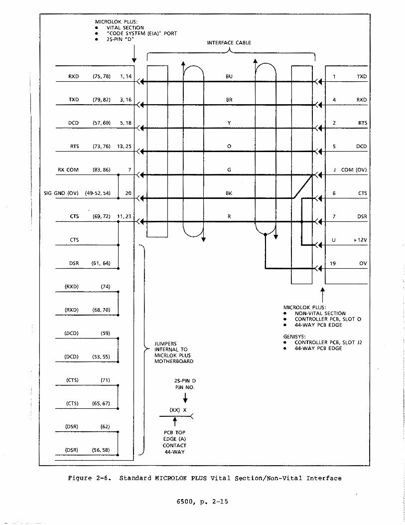
MICROLOK PLUS: • VITAL SECTION • "CODE SYSTEM (EIA)" PORT • 25-PIN "D"
INTERFACE CABLE
·~ ·~ RXD (75, 78) 1, 14 ... BU
.ii 1 TXD
.... ,...,
TXD (79, 82) 3, 16 ... BR .ii
4 RXD ' .... ' ....
DCD (57, 60) 5, 18 ... y .ii
2 RTS
" .... ' ....
RTS (73, 76) 13, 25 ... 0 ... 5 DCD
'~ -~ RX COM (83, 86) 7 ... G ... J COM (OV)
SIG
~
/_ ~
GND (OV) (49-52, 54) 20 ... BK k·~
6 CTS ....
CTS (69, 72) 11,23 / ... R
.ii 7 DSR
, .... ' ....
~' ~' CTS u +12V - k·~
DSR (61, 64) ... 19 ov ' .....
(RXD} (74)
i (RXD) (68, 70) MICROLOK PLUS:
• NON-VITAL SECTION
• CONTROLLER PCB, SLOT O
• 44-WA Y PCB EDGE
(DCD} (59) GENISYS:
JUMPERS • CONTROLLER PCB, SLOT J2
INTERNAL TO • 44-WA Y PCB EDGE
(DCD} (53, 55) MICRLOK PLUS MOTHERBOARD
(CTS) (71) 25-PIN D PIN NO .
(CTS) (65, 67) • (XX) X
t (
(DSR) (62) PCB TOP EDGE (A) CONTACT
(DSR) (56,58) ~ 44-WAY
Figure 2-6. Standard MICROLOK PLUS Vital section/Non-Vital Interface
6500, p. 2-15
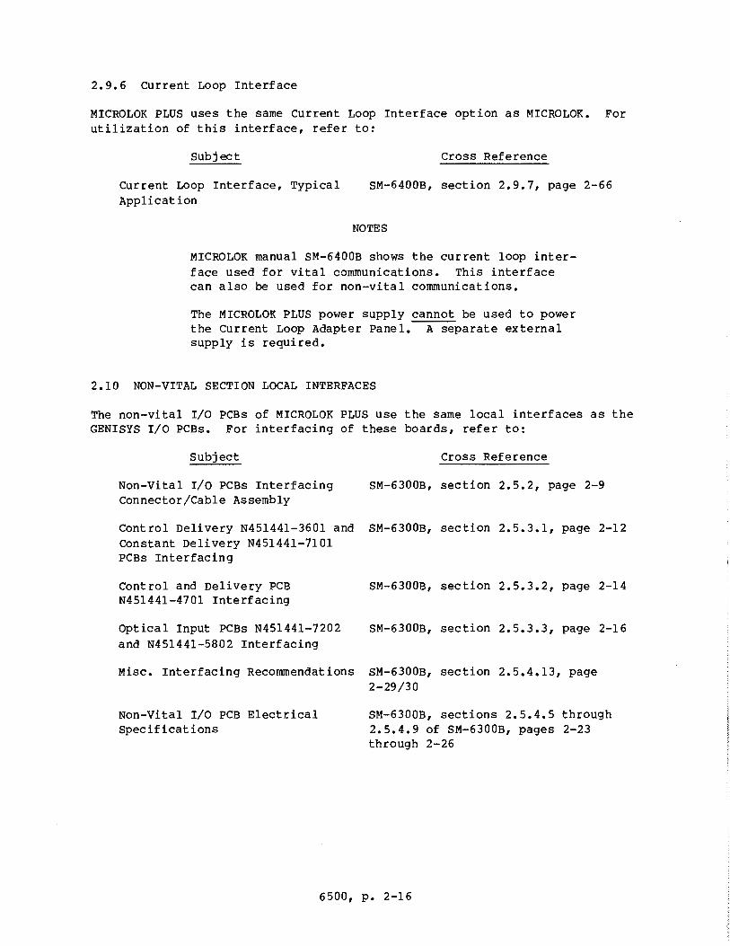
2.9.6 current Loop Interface
MICROLOK PLUS uses the same Current Loop Interface option as MICROLOK. For utilization of this interface, refer to:
Cross Reference
Current Loop Interface, Typical Application
SM-6400B, section 2.9.7, page 2-66
NOTES
MICROLOK manual SM-6400B shows the current loop interface used for vital communications. This interface can also be used for non-vital communications.
The MICROLOK PLUS power supply cannot be used to power the Current Loop Adapter Panel. A separate external supply is required.
2.10 NON-VITAL SECTION LOCAL INTERFACES
The non-vital I/0 PCBs of MICROLOK PLUS use the same local interfaces as the GENISYS I/0 PCBs. For interfacing of these boards, refer to:
Subject Cross Reference
Non-Vital I/0 PCBs Interfacing SM-6300B, section 2.5.2, page 2-9 Connector/Cable Assembly
Control Delivery N451441-3601 and SM-6300B, section 2.5.3.1, page 2-12 Constant Delivery N451441-7101 PCBs Interfacing
Control and Delivery PCB SM-6300B, section 2.5.3.2, page 2-14 N451441-4701 Interfacing
Optical Input PCBs N451441-7202 SM-6300B, section 2.5.3.3, page 2-16 and N451441-5802 Interfacing
Misc. Interfacing Recommendations SM-6300B, section 2.5.4.13, page 2-29/30
Non-Vital I/0 PCB Electrical SM-6300B, sections 2.5.4.5 through Specifications 2.5.4.9 of SM-6300B, pages 2-23
through 2-26
6500, p. 2-16
2.11 NON-VITAL SECTION SERIAL INTERFACE SPECIFICATIONS
NOTE
See Figure 2-5 for physical arrangement of all MICROLOK PLUS serial data ports and cables.
The following table summarizes the interface options available to the non-vital section Controller PCB:
Interface To
External MICROLOK PLUS
External MICROLOK PLUS
External MICROLOK
External GENISYS
Office Computer
Same MICROLOK PLUS
Remote Port Modem Options
Controller PCB (Non-Vital Section) EIA or TTL (Master and Satellite ports)
Code System PCB (Vital Section) EIA Only
Code System PCB EIA or TTL
Controller PCB EIA or TTL (Master and Satellite ports)
EIA or TTL
Code System PCB (Vital Section) EIA Only
The non-vital Controller PCB of MICROLOK PLUS use the same serial interfaces as the GENISYS Controller PCB. For interfacing of this board, refer to:
Subject Cross Reference
Master/Satellite System Configua- SM-6300B, section 2.4, page 2-7 tion Guidelines
Non-Vital Controller PCB (N451441-5602) Connector/Cable Assembly
Non-Vital Controller PCB (N451441-5602) Interfacing
Non-Vital Controller PCB (N451441-5602) Electrical Specifications
SM-6300B, section 2.5.2, page 2-9
SM-6300B, section 2.5.3.4, page 2-18
SM-6300B, section 2.5.4.4, page 2-22
6500, p. 2-17/18

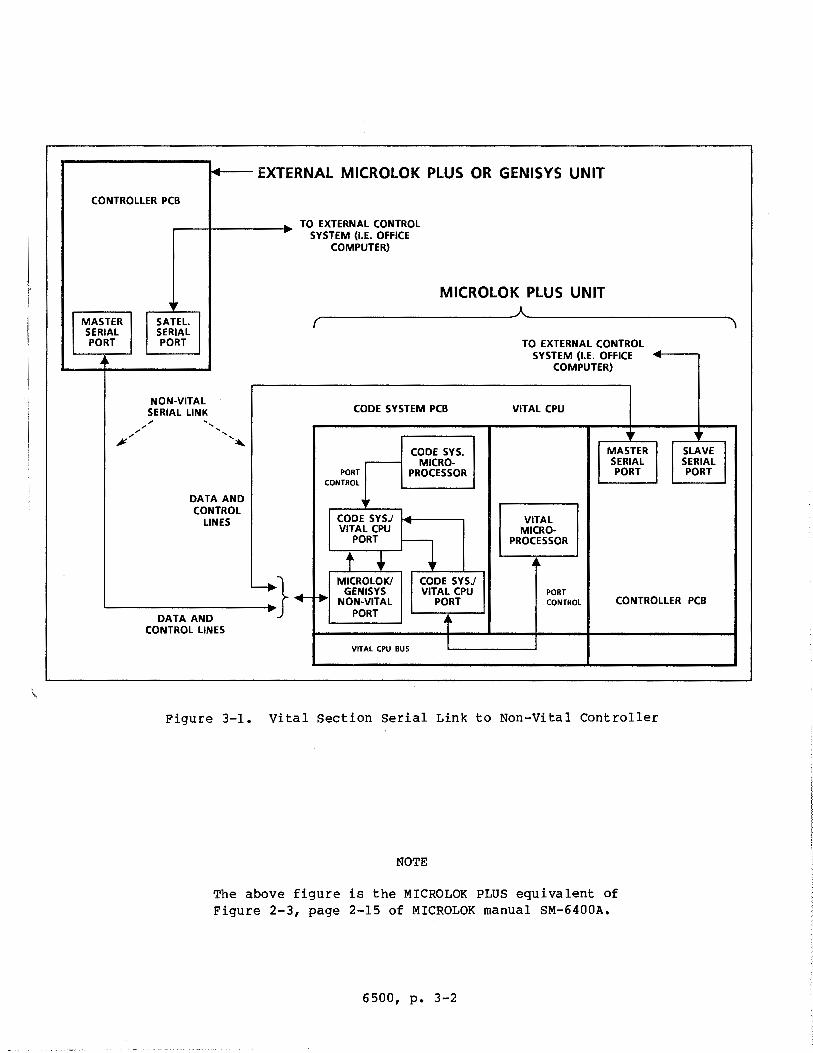
SECTION III FUNCTIONAL DESCRIPTION
3.1 VITAL SECTION
The MICROLOK PLUS vital section utilizes the same operating principles as the MICROLOK system. For functional descriptions, refer to:
Subject
Basic Vital Operating Principles
Non-Vital Serial Communications
Cross Reference
SM-6400A, sections 2.1 through 2.3, pages 2-1 through 2-11
SM-6400A, section 2.5, pages 2-14 through 2-17/18
NOTES
Section 2.4: This section describes the redundant CPU function of MICROLOK. Since MICROLOK PLUS cannot be equipped with redundant CPUs, section 2.4 is not applicable.
Figure 3-1 on the following page is MICROLOK PLUS equivalent of Figure 2-3, page 2-15, of MICROLOK manual SM-6400A.
3.2 NON-VITAL SECTION
The MICROLOK PLUS non-vital section utilizes the same operating principles as the GENISYS system. For functional descriptions, refer to:
Subject
Serial Port Operation Data and Control Lines LEDs carrier Control Modes
Controller PCB (N451441-5602) Functions
Relay-Output PCBs (N451441-3601) and N451441-7101 Functions
Relay-Output PCB (N451441-4701) Functions
Optical Input PCBs (N451441-7202) and N451441-5802 Functions
Cross Reference
SM-6300B, section III, pages 3-1 through 3-7/8
SM-6300C, section 2.1, pages 2-1 through 2-9
SM-6300C, section 2.2.1, pages 2-10 through 2-13/14
SM-6300C, section 2.2.2, pages 2-16 through 2-17/18
SM-6300C, section 2.3, pages 2-20 through 2-23/24
6500, p. 3-1
--- EXTERNAL MICROLOK PLUS OR GENISYS UNIT
CONTROLLER PCB
MASTER SERIAL PORT
~--+-----• TO EXTERNAL CONTROL SYSTEM (I.E. OFFICE
COMPUTER)
MICROLOK PLUS UNIT
SA TEL. SERIAL PORT
NON-VITAL SERIAL LINK
DATA AND CONTROL
LINES
CODE SYSTEM PCB
CODE SYS. ~ MICRO-
PORT PROCESSOR CONTROL
,Ir
CODE SYSJ ~ ... VITAL CPU
PORT
-i t .. MICROLOK/ CODE SYSJ
GENISYS VITAL CPU
TO EXTERNAL CONTROL SYSTEM (I.E. OFFICE
COMPUTER)
VITAL CPU
,. MASTER SERIAL PORT
VITAL MICRO-
PROCESSOR
a
PORT
~
~
,, SLAVE SERIAL PORT
~}.-~ NON-VITAL PORT CONTROL CONTROLLER PCB
DATA AND CONTROL LINES
PORT
VITAL CPU BUS
t I
Figure 3-1. Vital Section Serial Link to Non-Vital Controller
NOTE
The above figure is the MICROLOK PLUS equivalent of Figure 2-3, page 2-15 of MICROLOK manual SM-6400A.
6500, p. 3-2
SECTION IV APPLICATION PROGRAMMING
4.1 VITAL SECTION
The MICROLOK PLUS vital section uses the same application logic as the MICROLOK system. For programming procedures and guidelines, refer to:
Subject Cross Reference
Programming Formats, Guidelines SM-6400A, sections 3.1 through 3.6, pages 3-1 through 3-28
MICROLOK Development System Introduction
SM-6400A, sections 3.7 through 3.12, pages 3-29 through 3-58
Files Compiler Simulator EPROM Programmer Scan Time Estimates
Supplemental Data Application Logic Compiler Switches Status Byte Allocation in Non-Vital Controller Compiler Error Messages
SM-6400A, section IV, pages 4-1 through 4-12
NOTES
The MICROLOK Development System compiler permits up to 15 I/0 PCBs to be defined. However, the MICROLOK PLUS vital section only allows 10 vital I/0 PCBs. This aspect of MICROLOK PLUS programming should be noted in the following sections of SM-6400A:
Section
3.3.1.3, part B 3.5, step 4
3-10 3-24
Section 4.3.3, page 4-11 of SM-6400A: Semantic Error Code number 10 will be displayed when more than 15 local I/0 boards are specified. However, no error will be displayed if 11 to 15 local I/0 boards are specified for MICROLOK PLUS.
Figures 4-1 and 4-2 on the following pages show a sample symbol table and source listings for a MICROLOK PLUS vital section application program. Refer to these listings in place of of the listings on pages 3-34 and 3-35 of SM-6400A.
6500, p. 4-1
MICROLOK SOURCE LISTING ( VERSION 4.00) 18-APR-1989 COPYRIGHT 1985, REVISED 1989 UNION SWITCH & SIGNAL INC.
1 %$D+ DEBUG ON' 2 % THIS IS A SAMPLE PROGRAM\ 3 4 %$Ll 1 MINUTE RESET OUTPUT INHIBIT TIME'\ 5 6 MICROLOK PROGRAM EXAMPLEl; 7 8 INTERFACE 9 LOCAL
10 OUTPUT DC.STANDARD WORD: 01,02,03; 11 OUTPUT DC.LAMP WORD: Ll,L2,L3; 12 LAMPOUT: L01,L02,L03; 13 INPUT DC.STANDARD WORD: Il, I2, I3, I4, IS, I6; 14 15 VAR 16 Vl; 17
TIMER Vl 01 03
SET=lOO:MSEC SET=56 0 :MSEC SET=O:MSEC
CODED OUTPUT TOGGLE L2 AT 10:CPM
20:CPM
BEGIN ASSIGN Il ASSIGN Il AND I2 ASSIGN I3 XOR I2 ASSIGN I6
IF IF
CLEAR=lOO:MSEC; CLEAR=SO:MSEC; CLEAR=SO:MSEC;
I3; I4;
TO 01; TO 02; TO 03, Vl; TO L3;
18 19 20 21 22 23 24 25 26 27 28 29 30 31 32 33
ASSIGN L2 AND (I3 or I4) TO Ll; END
ERRORS DETECTED : 0 UNASSIGNED INTERNAL/OUTPUT BITS 3
PAGE:
Figure 4-1. Sample Source Listing for MICROLOK PLUS Vital Section Application Program
6500, p. 4-2
1
'-.:! ..... <Q s;::: rs Cl)
""' I 1-J .
:i:,, Cl)
:g !!J 1--''0 ..... I-' n Cl) QJ rt Cl) ..... '< 0 :I ::s tr
0 'i:::t I-' rs 0 8
<Q QJ O'I rs tr l11 QJ I-' 0 :I Cl) 0 .. I:"' .....
'Cl rn . rt" ..... ""' ::s I <Q w
111 0 rs :;:: H ()
~ I:"'
~ 'i:::t
8 Cl)
<: ..... rt QJ I-'
Cl) Cl) n rt ..... 0 ::s
MlCROL.OK Symbol Table Listing [ Vers i ,:,n 4.00
Bit Bit Bit Equations Using Nurnbet· Name Type Front Back
01 OUTPUT 2 02 OUTPUT 3 0:3 OUTPUT 4 L1 OUTPlJT 5 L';> OUTPUT 1 0 6 L:3 OUTPUT 7 L01 SYSTEM BIT 8 L02 SYSTEM BIT 9 UJ::::: SYSTEM BIT
10 11 INPUT 2 0 11 I·" '- INPUT 2 0 12 1·-:> •J INPUT 2 0 1:3 14 INPUT 1 (I
14 15 INPUT 15 16 INPUT 1 0 11.::, V1 INTERNAL 17 KILL *UNASSIGNED 18 RESET *UNASSIGNED 19 SYSERR.CLEAR *UNASSIGNED 20 SYSERR SYSTEM BIT 21 SYSERR.1 SYSTEM BIT ·":--":-"-"- SYSERR.2 SYSTEM BIT 23 SYSERR.3 SYSTEM BIT 24 SYSERR.4 SYSTEM BIT :2:5 SYSERR.5 SYSTEM BIT 26 SYSERR.6 SYSTEM BIT 27 SYSERR.7 SYSTEM BIT 28 SYSERR.8 SYSTEM BIT 29 SYSERR.9 SYSTEM BIT :30 SYSERR.10 SYSTEM BIT
MICROLOK Symbol Table Listing Version 4.00 J
Bit Number
Bit Name
SWITCH Settings
Debus Initial Output Delay MIP Sum No Response Time MASTER
Time Out Baud Rate f<ey On Key Off
SLAVE Time Out Baud Rate f<ey On Key Off
Bit Type
ON 1 MIN 1.0 SEC 116 MSEC
4.0 SEC 1200 BPS O MSEC O MSEC
4.0 SEC 1200 BPS O MSEC O MSEC
Equations Using Front Back
Program: "E}(AMPLE1
Intet·face Inf,)nnat ion Type Station Position
LOCAL 1 0 LOCAL 1 1 LOCAL 1 2 LOCAL 2 0 LOCAL 2 1 LOCAL 2 2
LOCAL 3 0 LOCAL 3 1 LOCAL 3 2 LOCAL 3 3 LOCAL 3 4 LOCAL 3 5
Program: "EXAMPLE1
Interface Information Type Station Position
Bit Attribute
TIMER BIT
TIMER BIT
CODED OUTPUT
TIMER BIT
II
Bit Attribute
Page: SYM-1
Time Delay Set Clear
560:MSEC 50:MSEC
O:MSEC 50:MSEC
100:MSEC 100:MSEC
Page: SYM-2
Time Delay Set Clear
4.2 NON-VITAL SECTION
The MICROLOK PLUS non-vital section uses the same application logic as the GENISYS system. For programming procedures and guidelines, refer to:
Subject
Programming Formats, Guidelines
GENISYS Development System Introduction Files Compiler Simulator EPROM Size Estimates Program EPROM Programmer
Program Design Notes Logic and Timing Overflows Timing Elements Validation Option Logic Queuing and Execution
Misc. Application Information Local I/0 serial communications Timing
Serial Communications Protocols Introduction to Formats Detailed Descriptions
Error/Warning Messages Token and Parsing Semantic
Cross Reference
SM-6300A, sections 2.1 and 2.2, pages 2-1 through 2-23
SM-6300A, sections 2.3 through 2.8, pages 2-24 through 2-60
SM-6300A, section III, pages 3-1 through 3-7/8
SM-6300A, section IV, pages 4-1 and 4-2
SM-6300A, section V, pages 5-1 through 5-10
SM-6300A, sections 6.1 and 6.2, pages 6-1 through 6-4.
NOTES
The GENISYS Development System compiler permits up to 16 I/0 PCBs to be defined. However, the MICROLOK PLUS non-vital section only allows two I/0 PCBs. This aspect of MICROLOK PLUS programming should be noted in the following sections of SM-6300A:
Section
2.2.3.1 2 • 7 • 1 , " NI OB " 2.7.2, "How many local I/0 boards?"
2-8 2-50 2-51
Section 6.2, page 6-21 of SM-6300A: Semantic Error Code number 1 will be displayed when more than 16 local I/0 boards are specified. However, no error will be displayed if 3 to 16 local I/0 boards are specified for MICROLOK PLUS.
6500A, p. 4-4
NOTES (Cont'd)
Figures 4-3 and 4-4 on the following pages show sample symbol table and source listings for a MICROLOK PLUS non-vital section application program. Refer to these listings in place of of the listings on pages 2-30 and 2-31 of SM-6300A.
In the Symbol Table Listing, note that the I/0 slots are numbered 3 and 4. These are the first two slot numbers used in the GENISYS compiler. In MICROLOK PLUS these slots are numbered P and Q.
6500, p. 4-5
GENISYS SOURCE LISTING VERSION 2.06 20-MAR-1989
1 2 3 4 5 6 7 8 9
10 11 12 13 14 15 16 17 18 19 20 21 22 23 24 25 26 27 28 29 30 31 32 33 34 35 36 37
COPYRIGHT 1984 - 1988, UNION SWITCH & SIGNAL, INC.
%
\
THIS IS AN EXAMPLE OF A BASIC GENISYS PROGRAM.
%$D+ %$Q+
DEBUG ON\ TWO QUEUE OPTION\
PROGRAM NBR3; INTERFACE
LOCAL OUTPUT WORD: OUT.I, OUT.2, OUT.3,
SPARE, SPARE, SPARE, SPARE, SPARE, OUT.4, OUT.5, OUT.6, OUT.7, OUT.8;
INPUT WORD: IN.A, IN.B, IN.C, IN.D;
VAR STICK, Tl;
TIMER Tl: OUT.7 OUT.8
BEGIN
SET=l:SEC SET=l:SEC SET=O:SEC
ASSIGN IN.A AND IN.B ASSIGN IN.A XOR IN.B ASSIGN IN.A OR IN.B ASSIGN NOT IN.A
CLEAR=l:SEC; CLEAR =l:SEC; CLEAR =500:MSEC;
ASSIGN IN.C OR (STICK AND NOT IN.D) ASSIGN STICK
TO OUT. l; TO OUT.2; TO OUT.3; TO OUT.4; TO STICK; TO OUT.6; TO Tl; ASSIGN NOT Tl
ASSIGN Tl ASSIGN NOT Tl
END
TO OUT.7; TO OUT.8;
WARNINGS DETECTED: 0 ERRORS DETECTED: 0
Figure 4-3. Sample source Listing for MICROLOK PLUS Non-Vital Section Application Program
6500, p. 4-6
PAGE 1
BIT SYMBOL TABLE FOR "NRB3"
IDENTIFIER BIT NUMBER & TYPE
LOCAL I/0 BOARDS OUTPUT - SLOT 3
OUT.l 1 OUTPUT OUT.2 2 OUTPUT OUT.3 3 OUTPUT SPARE 4 SPARE 5 SPARE 6 SPARE 7 SPARE 8 OUT.4 9 OUTPUT OUT.5 10 UNASSIGNED OUT.6 11 OUTPUT OUT.7 12 OUTPUT OUT.8 13 OUTPUT
INPUT - SLOT 4 IN.A 14 INPUT IN.B 15 INPUT IN.C 16 INPUT IN.D 17 INPUT
LOCAL VARS STICK 18 INTERNAL Tl 19 INTERNAL
SWITCH SETTINGS
SLAVE BAUD RATE MASTER BAUD RATE POLLING TIME OUT CONTROL DELIVERY TIME SECURITY DEBUG SYMBOL TABLE LISTING VALIDITY CHECK TWO QUEUE OPTION
HARDWARE SWITCH 1200 BPS 1000 MSEC HARDWARE SWITCH AUTOMATIC ON ON ON ON
20-MAR-1989. PAGE SYM- 1
TIMER SET
1.0: SEC 0.0: MSEC
1.0: SEC
CLEAR
1. 0: SEC 400.0: MSEC
1. 0: SEC
Notes: "OUTPUT - SLOT 3" is slot "P" in MICROLOK PLUS cardfile. "INPUT - SLOT 4" is slot "Q" in MICROLOK PLUS cardfile.
Figure 4-4. Sample Symbol Table for MICROLOK PLUS Non-Vital Section Application Program
6500, p. 4-7/8

5.1 VITAL SECTION
5.1.1 General Requirements
SECTION V FIELD MAINTENANCE
The MICROLOK PLUS unit is subject to the same general maintenance requirements as the MICROLOK system. For these requirements, refer to:
Subject Cross Reference
Gene·-·al Maintenance Requirement SM-6400C, section 3.1, page 3-1
NOTE
The MICROLOK PLUS power supply drawer is subject to the same maintenance requirements as the MICROLOK CPU and I/0 power supplies. No attempt should be made to shop repair the drawer in the field. The drawer should be returned to US&S for repair or
eplacement.
5.1.2 Periodic Inspection
For periodic inspection of the MICROLOK PLUS unit, refer to:
Subject Cross Reference
Periodic Inspection SM-6400C, section 3.2, page 3-2
5.1.1 Troubleshooting Guide
5.1.3.l Required Test Equipment and Materials
The M!CROLOK PLUS unit uses the same test equipment and materials as the MICROLOK system. For a listing of these items, refer to:
Subject
Required Test Equipment and Materials
Cross Reference
SM-6400C, section 3.3.1, page 3-3
6500, p. 5-1
5.1.3.2 Power-Off Checks
The power-off checks of the MICROLOK PLUS unit are the same as those for the MICROLOK system. For these checks, refer to:
Subject Cross Reference
Power-Off Checks SM-6400C, section 3.3.2, pages 3-4 and 3-5
NOTES
Step 1: Unlike the MICROLOK system, the order of the vital CPU boards in MICROLOK PLUS is fixed.
Step 4: This step only lists the vital I/0 boards without individual I/0 line LEDs. The equivalent boards with I/0 line LEDs are as follows:
Standard Relay Driver Voltage-Limited Relay Driver Bipolar Relay Driver Standard Input Standard Input
US&S Part No. N451441-
w/o LEDs w/LEDs
-6501 -8601 -7401 -8501 -6601 -8701 -6402 -8802 -6403 -8803
Step 5: The Echo Enable jumpers on MICROLOK PLUS are labelled differently than the MICROLOK CPU cardfile. Refer to section 2.7 of this manual when performing the jumper position check.
Refer to Figure 1-4 of this manual in place of Figure 3-1 of SM-6400C.
5.1.3.3 Power-On Checks
The power-on checks of the MICROLOK PLUS unit are the same as those for the MICROLOK system. For these checks, refer to:
Subject
Power-On Checks
Cross Reference
SM-6400C, section 3.3.3, pages 3-7 and 3-8
6500, p. 5-2
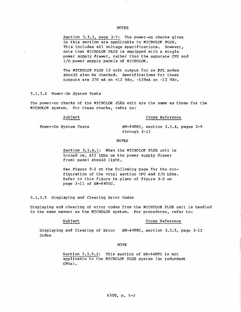
NOTES
Section 3.3.3, page 3-7: The power-on checks given in this section are applicable to MICROLOK PLUS. This includes all voltage specifications. However, note that MICROLOK PLUS is equipped with a single power supply drawer, rather than the separate CPU and I/0 power supply panels of MICROLOK.
The MICROLOK PLUS 12 volt output for an RFL modem should also be checked. Specifications for these outputs are 270 mA on +12 Vdc, -135mA on -12 Vdc.
5.1.3.4 Power-On System Tests
The power-on checks of the MICROLOK PLUS unit are the same as those for the MICROLOK system. For these checks, refer to:
Subject
Power-On System Tests
Cross Reference
SM-6400C, section 3.3.4, pages 3-9 through 3-11
NOTES
Section 3.3.4.1: When the MICROLOK PLUS unit is turned on, all LEDs on the power supply drawer front panel should light.
See Figure 5-1 on the following page for the configuration of the vital section CPU and I/0 LEDs. Refer to this figure in place of Figure 3-2 on page 3-11 of SM-6400C.
5.1.3.5 Displaying and Clearing Error Codes
Displaying and clearing of error codes from the MICROLOK PLUS unit is handled in the same manner as the MICROLOK system. For procedures, refer to:
Subject
Displaying and Clearing of Error Codes
Cross Reference
SM-6400C, section 3.3.5, page 3-12
NOTE
Section 3.3.5.2: This section of SM-6400C is not applicable to the MICROLOK PLUS system (no redundant CPUs).
6500, p. 5-3
',;l ..... t.Q s::: l"'I <D
U1 I ~ . : n 0 ::, HI
°' .....
u, t.Q 0 s::: 0 l"'I'
... ~ 'U
..... 0 ::,
u, I 0
"'" HI
~ ..... rt DI 1--'
Cl)
<D (')
rt ..... 0 ::,
t"' t>l t:, en
RED
LED
NO.
t
ORANGE
LED
NO.
+
YELLOW WHITE BLUE
DLED NO. .. !
LED
NO.
t 7 (RTS)
8 (WTCHDG)
1 (DCD}
2 (DIAG.)
3 (DIAG.)
4 (DIAG)
5 (DIAG.)
6 (DIAG.)
7 (WTCHDG)
6 (NOT USED}
5 (NOT USED}
LED
NO.
! 4 (SYS. STAT.) NO.
3 (SYS. STAT.) + 2 (SYS. STAT.)
BLUE PINK PINK AQUA AQUA VIOLET GREEN GREEN
D D D D D D D 9 (INRUSH 1)
8 (VOLT. 1)
7 (INRUSH 2)
6 (VOLT. 2)
5 (INRUSH 3)
4 (VOLT. 3)
LED LED
II II I~ 3 (INRUSH 4} NO. NO. 2 (VOLT. 4)
+ t 2 (INPUT 1)
2 (OUTPUT 1) 2 (OUTPUT 1) 2 (OUT IN} 3 (INPUT 2)
3 (OUTPUT 2) 3 (OUTPUT 2) 3 (OUT IR 4 (INPUT 3)
4 (OUTPUT 3) 4 (OUTPUT 3) 4 (OUT 2N} 5 (INPUT 4)
5 (OUT 2R) LED LED 5 (OUTPUT 4) 5 (OUTPUT 4) NO. NO. 6 (INPUT 5)
6 (OUTPUT 5) 6 (OUTPUT 5) 6 (OUT 3N)
+ + 7 (INOUT 6)
7 (OUTPUT 6) 7 (OUTPUT 6) 7 (OUT 3R) 8 (INPUT 7)
1 (BD. ADR.) 1 (BD. ADR.) 9 (INPUT 8)
NO. NO. NO. NO. NO. NO.
1 (CLOCK) 1(0N·LINE)
l= 1 (SYS. STAT.) 1 (BD. ADR.}
l"" ~ (BD. ADR.}
l"" ~ (BD. ADR.)
l "" ~ (SD. ADR.)
l "" ~ (BD. ADR.)
l"" ~ (BD. ADR.)
l"" ~ (BD. ADR.}
PROCESSOR 1/0 BUS CODE SYS. PERIPHERAL STANDARD STANDARD VOL T.-LIMIT. VOLT.-LIMIT. Bl-POLAR Bl-POLAR DC LAMP STANDARD STANDARD N451441- INTERFACE INTERFACE N451441- RELAY RELAY RELAY RELAY RELAY RELAY DRIVER INPUT INPUT
5701 N451441- N451441- 5502 DRIVER DRIVER DRIVER DRIVER DRIVER DRIVER N451441· N451441- N451441-6001 5302 N451441- N451441- N451441- N451441- N451441- N451441- 6702, 6703, 6402, 6403, 8802, 8803
6501 8601 7401 8501 6601 8701 7301
SLOT A SLOT B SLOT C SLOT D SLOTS E-N SLOTS E-N SLOTS E-N SLOTS E-N SLOTS E-N SLOTS E-N SLOTS E-N SLOTS E-N SLOTS E-N
r VITAL CPU VITAL 1/0 ~, SEE FIG. 5-3 FOR NON-VITAL PCB LEDS
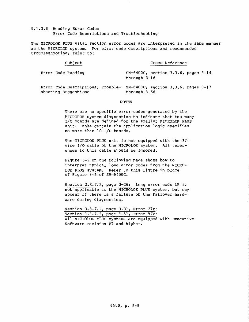
5.1.3.6 Reading Error Codes Error Code Descriptions and Troubleshooting
The MICROLOK PLUS vital section error codes are interpreted in the same manner as the MICROLOK system. For error code descriptions and recommended troubleshooting, refer to:
Subject
Error Code Reading
Cross Reference
SM-6400C, section 3.3.6, pages 3-14 through 3-16
Error Code Descriptions, Troubleshooting Suggestions
SM-6400C, section 3.3.6, pages 3-17 through 3-56
NOTES
There are no specific error codes generated by the MICROLOK system diagnostics to indicate that too many I/0 boards are defined for the smaller MICROLOK PLUS unit. Make certain the application logic specifies no more than 10 I/0 boards.
The MICROLOK PLUS unit is not equipped with the 37-wire I/0 cable of the MICROLOK system. All references to this cable should be ignored.
Figure 5-2 on the interpret typical LOK PLUS system. of Figure 3-5 of
following page shows how to long error codes from the MICRORefer to this figure in place
SM-6400C.
Section 3.3.7.2, page 3-26: Long error code lE is not applicable to the MICROLOK PLUS system, but may appear if there is a failure of the failover hardware during diagnostics.
Section 3.3.7.2, page 3-31, Error 27x: Section 3.3.7.2, page 3-51, Error 97x: All MICROLOK PLUS systems are equipped with Executive Software revision #7 and higher.
6500, p. 5-5
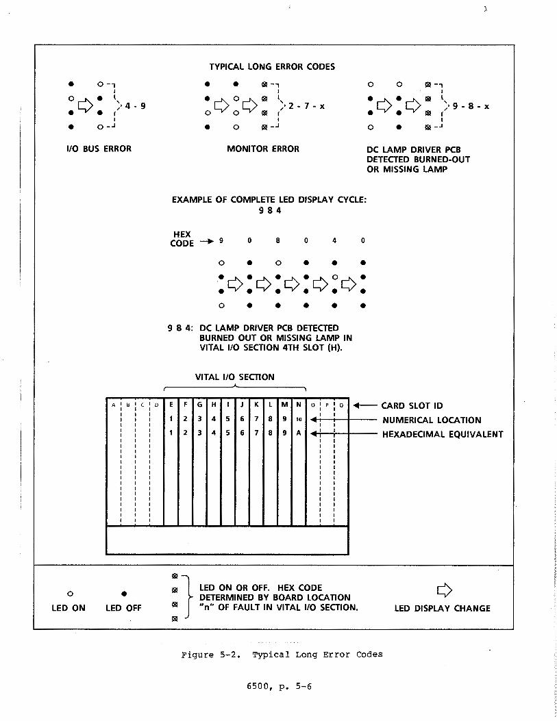
• 0 -, I
0 • l r-1'. >4-9
eY • ' I
• o-.J
1/0 BUS ERROR
0
LED ON
A B I C I D I I I I I I I I I I I I I I I I I I I I I I I I I I I I I I I I I I I I I I I I I I I I
• LED OFF
I
TYPICAL LONG ERROR CODES
• • 181 -, I
erl\,.Orl\,.l8I \2-7-x oYoYl!!! r
I
e O 181-.J
MONITOR ERROR
EXAMPLE OF COMPLETE LED DISPLAY CYCLE: 984
HEX CODE~ 9
0
0
• 8
0
0 4 0
• • • .• r-1'. • r-1'. • r-1'. • r-1'. 0 r-1'. • eYeYeYeYeYe
0 • • • • 9 8 4: DC LAMP DRIVER PCB DETECTED
BURNED OUT OR MISSING LAMP IN VITAL 1/0 SECTION 4TH SLOT (H).
VITAL 1/0 SECTION l
•
0 0 !SI -, I
•¢•¢181 l '• 9 - 8 - x • • 181 ,~ I
0 • !SI _.J
DC LAMP DRIVER PCB DETECTED BURNED-OUT OR MISSING LAMP
E F G H K L M N o P o .__ CARD SLOT ID
2 3 4 5
2 3 4 5
6 7 8 9 10 4.,1-+--+---t---
6 7 8 9 A -, I I
:1 !SI
LED ON OR OFF. HEX CODE DETERMINED BY BOARD LOCATION "n" OF FAULT IN VITAL 1/0 SECTION.
Figure 5-2. Typical Long Error Codes
6500, p. 5-6
NUMERICAL LOCATION
HEXADECIMAL EQUIVALENT
LED DISPLAY CHANGE
5.1.3.7 PCB Descriptions
The circuit and functional descriptions of the MICROLOK PLUS vital section PCBs are the same as those for the MICROLOK system. For these descriptions, refer to:
Subject
Processor PCB (N451441-5701) Description
Peripheral PCB (N451441-5502) Description
Cross Reference
SM-6400C, section 3.3.8.1, pages 3-57 through 3-59
SM-6400c, section 3.3.8.2, pages 3-60 through 3-63
NOTE
Page 3-60: Part B, section b: The failover hardware is present on the Peripheral board used in the MICROLOK PLUS unit, however this hardware is not used by the system.
Figure 3-7, page 3-63: The LOCK ON/AUTO/LOCK OFF switch (SW5) is not used in MICROLOK PLUS. However, always keep this switch in the AUTO position. If the LOCK LED is on, SW5 is not in the required AUTO position.
I/0 Bus Interface PCB (N451441-6001) Description
Code System Interface PCB (N451441-5302) Description
SM-6400C, section 3.3.8.3, pages 3-64 through 3-66
SM-6400C, section 3.3.8.4, pages 3-67 through 3-71
NOTE
The descriptions of the Code System PCB Interface to an external GENISYS unit also apply to an intra-unit interface to the MICROLOK PLUS non-vital section.
6500, p. 5-7
Subject Cross Reference
Vital I/0 PCB Descriptions SM-6400C, sections 3.3.8.5 through 3.3.8.8, pages 3-72 through 3-87.
NOTE
SM-6400C only describes the vital I/0 boards without out individual I/0 line LEDs. However, these descriptions are also applicable to the boards that are equipped with the line LEDs. Equivalent boards are as follows:
Standard Relay Driver Voltage-Limited Relay Driver Bipolar Relay Driver Standard Input Standard Input
US&S Part No. N451441-
w/o LEDs w/LEDs
-6501 -8601 -7401 -8501 -6601 -8701 -6402 -8802 -6403 -8803
Each of the "-8000" series boards is equipped with eight output monitoring LEDs. A given LED lights when the respective circuit is energized. See Figure 5-1 for the configurations of these LEDs.
6500, p. 5-8
5.1.3.8 Code System Interface Troubleshooting
The MICROLOK PLUS system uses the same Code System interface troubleshooting procedures as the MICROLOK system.
Subject
Code System Interface Troubleshooting
Cross Reference
SM-6400C, section 3.3.9, pages 3-90 through 3-107
NOTES
Section 3.3.9.2, part c, page 3-96: This section is not applicable to the MICROLOK PLUS system. All systems are equipped with Code System Executive Software revision 2 and higher.
The descriptions of the Code System PCB Interface to an external GENISYS unit also apply to an intra-unit interface to the MICROLOK PLUS non-vital section.
5.1.4 Retesting Guidelines
Retesting guidelines for the MICROLOK PLUS hardware and software are basically the same as those for the MICROLOK system. For these guidelines, refer to:
Subject
Hardware and Software Retesting Guidelines
Cross Reference
SM-6400C, section 3.4, pages 3-108 through 3-114
NOTES
Section 3.4.4, page 3-113: The I/0 Bus Interface cable checkout procedure is not applicable to the MICROLOK PLUS system.
Section 3.4.5, page 3-113: The power supply replacement procedure applies to the single MICROLOK PLUS power supply drawer.
Section 3.4.6, page 3-113: The cardfile replacement procedure applies to the single MICROLOK PLUS cardfile.
6500, p. 5-9
5.2 NON-VITAL SECTION
5.2.1 Basic Maintenance
Basic field maintenance of the MICROLOK PLUS non-vital section is the same as that for the GENISYS system. For maintenance recommendations, refer to:
Subject
Basic Maintenance of Non-Vital Section
5.2.2 Systematic Troubleshooting
5.2.2.1 Introduction
Cross Reference
SM-6300B, section v, page 5-1/2
The troubleshooting information referenced in this section is intended for new MICROLOK PLUS installations with a non-vital section that is experiencing start-up or initial operating difficulties. However, this section may also be used to troubleshoot problems with in-service MICROLOK PLUS installations.
All plug-in boards in the MICROLOK PLUS non-vital section, except the Controller PCB, may be directly swapped with spares, as long as the correct option is chosen for each type. A spare Controller PCB must contain the same application logic and hardware switch settings as the replaced board to insure proper system operation. Faulty boards may be returned to US&S for repair or replacement.
If repairing boards in the field, refer to SM-6300C (GENISYS) for board-level troubleshooting information.
5.2.2.2 Recommended Test and Repair Equipment
The MICROLOK PLUS non-vital section uses the same test and repair equipment as the GENISYS system. For a list of this equipment, refer to:
Subject
Test and Repair Equipment for Non-Vital Section
Cross Reference
SM-6300B, section 4.2, pages 4-2 through 4-4
6500C, p. 5-10
5.2.2.3 Initial Checks and Diagnostics Via Board LEDs
Initial checks of the MICROLOK PLUS non-vital section are the basically the same as those for the GENISYS system. For these checks, refer to:
Subject
Initial Checks of Non-Vital Section
LED Checks on Operational System
Cross Reference
SM-6300B, section 4.3, page 4-5
SM-6300B, section 4.4, pages 4-6 through 4-27/28
NOTES
Parts of this test procedure are written in accordance with the 15 I/0 slots of the GENISYS cardfile. The MICROLOK PLUS non-vital section has only two I/0 slots. Note this difference when performing the test procedure. For example, the non-vital I/0 section cannot have empty slots between boards.
The non-vital section of the MICROLOK PLUS unit is not equipped with a Power Supply Converter PCB. Board operating power is obtained from the power supply drawer. Where the GENISYS test procedure calls for turn-on and turn-off of the Power Supply Converter PCB, perform this step with the main power switch on the MICROLOK PLUS unit.
Figure 5-3 on the next page shows the configuration of the non-vital section LEDs. Refer to this figure in place of Figure 4-4 of SM-6300B.
Section 4.5, page 4-8: Steps 1 through 4 of this section are not applicable to MICROLOK PLUS. Use the following steps in their place:
1. Check the input voltage from the power source.
a. The input voltage should be in the range of 19.8 to 32.4 Vdc.
b. Make sure the supply current is sufficient and the voltage is steady when a load is placed on the supply.
2. Check the power supply converter module outputs by attaching a digital voltmeter ground to test point TP3 and the meter probe to test points TP4, TP5, TP6 and TP7. See Figure 2-3 on page 2-6 of this manual for locations.
6500, p. 5-11
WHITE
Dr~ D or~ D D or~ 1 (M TXD) 13 (BITS 1-4) 13 (BITS 1-4)
2 (M RTS) 14 (BITS 5-8) 14 (BITS S·B) 3 (M RXD)
4 (M DCD) Is (BITS 9·12) I s (BITS 9-12)
5 (S TXD) 16 (BITS 13·16) 16 (BITS 13·16) 6 (S RTS)
7 (S RXD)
8 (S DCD)
9 (WTCHDG.)
10 (DELIVER)
SEE FIGURE 5-1 FOR VITAL SECTION PCB LEDS.
LED
LED LED NO.
LED LED
NO. NO. t NO. NO.
t t t t 1 (ADDRESS)
2 (DELIVER) 2 (DELIVER) 1 (LO BYTE) 1 (LO BYTE)
2 (DELIVER)
1 (ADDRESS) 1 (ADDRESS) 2 (HI BYTE) 2 (HI BYTE)
CONTROLLER CONTROL CONSTANT CONTROL & INDICATION INDICATION N451441· DELIVERY DELIVERY DELIVERY OPTO OPTO
5602 N451441- N451441- N451441- N451441- N451441· 3601 7101 4701 5802 7202
SLOT O SLOTPORQ SLOTPORQ SLOTPORQ SLOTPORQ SLOT PORQ ,~ NON-VITAL 1/0
Figure 5-3. Configuration of Non-Vital Section LEDs
6500, p. 5-12
a. The power supply should show the following outputs:
TP4 = +5 Vdc, + 0.25 Vdc, -o.o Vdc TP5 = +12 Vdc, + 0.25 Vdc. TP6 = -12 Vdc, ~ o.25 Vdc. TP7 -5 Vdc, ±_ 0.25 Vdc.
b. If the 5 volt output on TP4 is out of specification, it may be adjusted using the procedure in section 2.4.4 of this manual.
c. If the 5 volt output cannot be brought into specification, or if any of the remaining outputs are out of specification, replace the power supply drawer with a good spare and repeat the test. If the readings do not repeat, the original unit is faulty and should be serviced.
5.3 POWER SUPPLY DRAWER
Field troubleshooting of the MICROLOK PLUS power supply drawer consists of making output voltage checks at test points within the drawer. Refer to the preceding section (5.2.2.3) for the test procedure. Do not attempt any field repairs to the supply. If output voltages are not to specification, replace the complete assembly and return the faulty unit to US&S for service.
6500, p. 5-13/14

6.1 VITAL SECTION PCBS
SECTION VI SHOP MAINTENANCE
US&S recommends against attempting shop repairs on any of the MICROLOK PLUS vital section PCBs. Such repairs might degrade the vital performance qualities of the system after the PCB is returned to service. Any repairs made to any vital CPU or vital I/0 PCBs within the warranty period will invalidate the warranty for the entire system.
6.2 NON-VITAL SECTION PCBS
Shop repairs of the MICROLOK PLUS non-vital section PCBs are the same as those for the GENISYS PCBs. For repair procedures, refer to the following:
Subject
Non-Vital PCBs - Shop Maintenance
6.3 POWER SUPPLY DRAWER
Cross Reference
SM-6300C, sections II and III
US&S recommends against attempting shop repairs on any of the MICROLOK PLUS power supply drawer, other than adjusting the 5 volt output (refer to section 2.4.4 of this manual). Such repairs might affect the performance of the vital section PCBs after the drawer is returned to service. Any repairs made to the power supply drawer within the warranty period will invalidate the warranty for the entire system.
6500, p. 6-1/2

it:CI UNION SWITCH '1\JJ & SIGNAL INC. A member of the ANSALDO Group 5800 Corporate Drive Pittsburgh, PA 15237
SERVICE MANUAL 6500
APPENDIX A
PARTS LIST
MICROLOK PLUS TM
VITAL PLUS NON-VITAL CONTROL PACKAGE
September, 1990 A-09/90-100-2882-1 ID0280F
COPYRIGHT 1990, UNION SWITCH & SIGNAL INC. PRINTED IN USA
AN SAL DO Trasporti
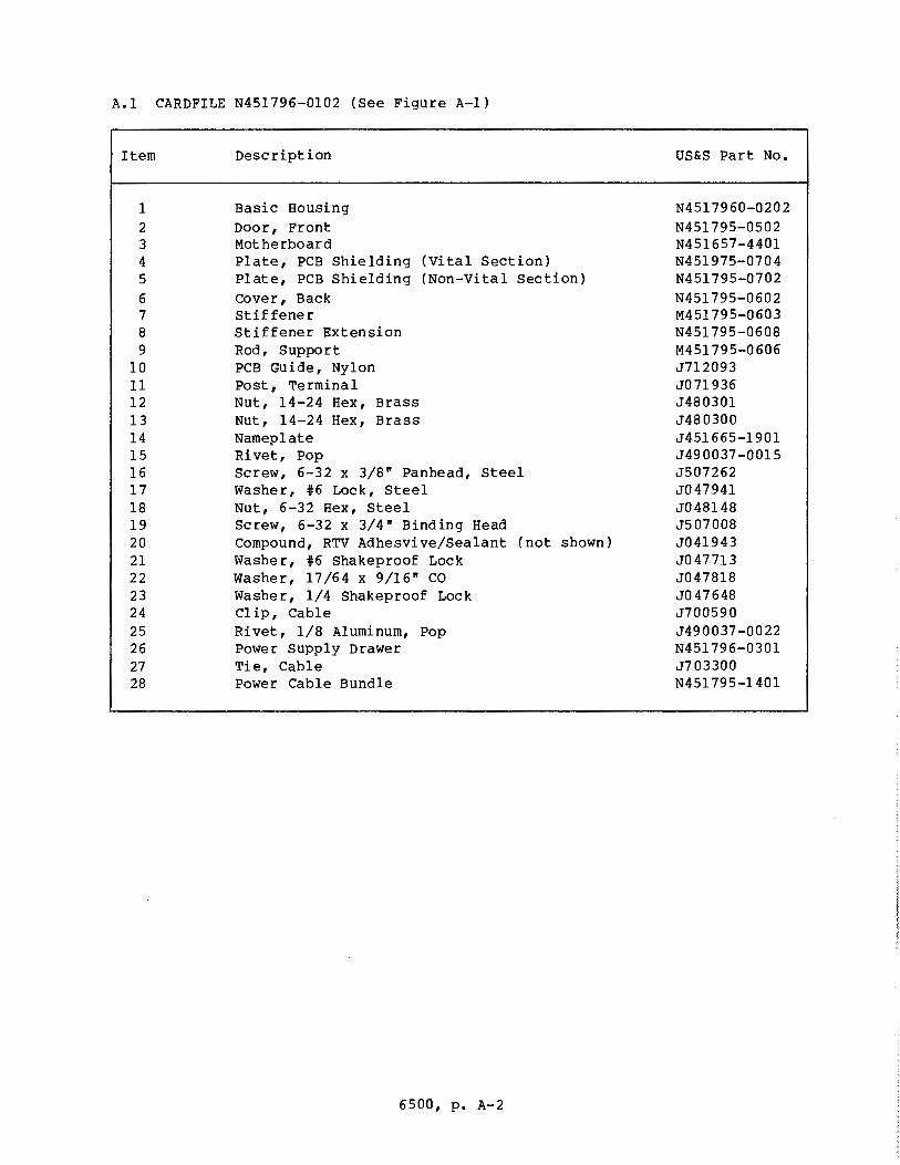
A.l CARDFILE N451796-0102 (See Figure A-1)
Item
1 2 3 4 5 6 7 8 9
10 11 12 13 14 15 16 17 18 19 20 21 22 23 24 25 26 27 28
Description
Basic Housing Door, Front Motherboard Plate, PCB Shielding (Vital Section) Plate, PCB Shielding (Non-Vital Section) Cover, Back Stiffener Stiffener Extension Rod, Support PCB Guide, Nylon Post, Terminal Nut, 14-24 Hex, Brass Nut, 14-24 Hex, Brass Nameplate Rivet, Pop Screw, 6-32 x 3/8n Panhead, Steel Washer, #6 Lock, Steel Nut, 6-32 Hex, Steel Screw, 6-32 x 3/4n Binding Head Compound, RTV Adhesvive/Sealant (not shown) Washer, #6 Shakeproof Lock Washer, 17/64 x 9/16n CO Washer, 1/4 Shakeproof Lock Clip, Cable Rivet, 1/8 Aluminum, Pop Power Supply Drawer Tie, Cable Power Cable Bundle
6500, p. A-2
US&S Part No.
N4517960-0202 N451795-0502 N451657-4401 N451975-0704 N451795-0702 N451795-0602 M451795-0603 N451795-0608 M451795-0606 J712093 J071936 J480301 J480300 J451665-1901 J490037-0015 J507262 JO 47941 J048148 J507008 J041943 J047713 J047818 J047648 J700590 J490037-0022 N451796-0301 J703300 N451795-1401
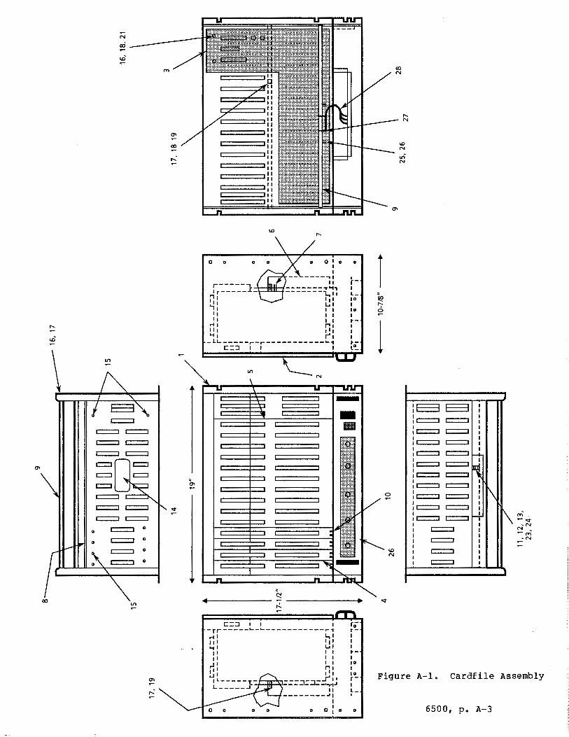
0
~
N
cxi
c:::::J
c:::::J c:::::J
c:::::J c::::::J
c::::::J c::::::J
c::::::J c::::::J
c::::::J O
0
0
0
.:iii c:====-;t!Hii
I I I I I I
0 0 0 O I o I I
-----,1
r-----, II I r-----i- --------.'-!, .,, -------1.,11
111 1,1 ,I ~: 1 1 I I 1 1 I I
~: r.: '-t I r' I -L~-----r-~-----------~~ C::J I I I
0
I r-1 LIO I IO I ~I I I ~L'!...
~--~--~ ....... \~~~~--:--------y-,r -
C::J I -rr-----~-~-----------r~ nl ~· 111 111 '-ti L..I
11 I I 11 I I
,JI I I 111 i.1 ,J I I I
I L-----T- ---::i-::i-I 1 1
L------'- --------•-:-i --------JI
I
-llllll1lll
r;; ~I I I ~I 10 I IO ,-1 L-
O O : 0 0
r
l
'° N
"' N
E::::::3 E::::::3 c::::::J c:::::J
c::::::J c::::::J
c::::::J c::::::J
c::::::J c:::::J
c::::::J c:::::J
c:::::J c:::::J
c:::::J c:::::J
c::::::J c::::::J
c:::::J c::::::J
c:::::J c::::::J
c::::::J
c::::::J
c::::::J
c:::::J
J I I I I I I I I I
1-1-
~ I I
f\ I I I I
I'\ ~ I I I I I I I I I
11
Figure A-1. cardfile Assembly
6500, p. A-3
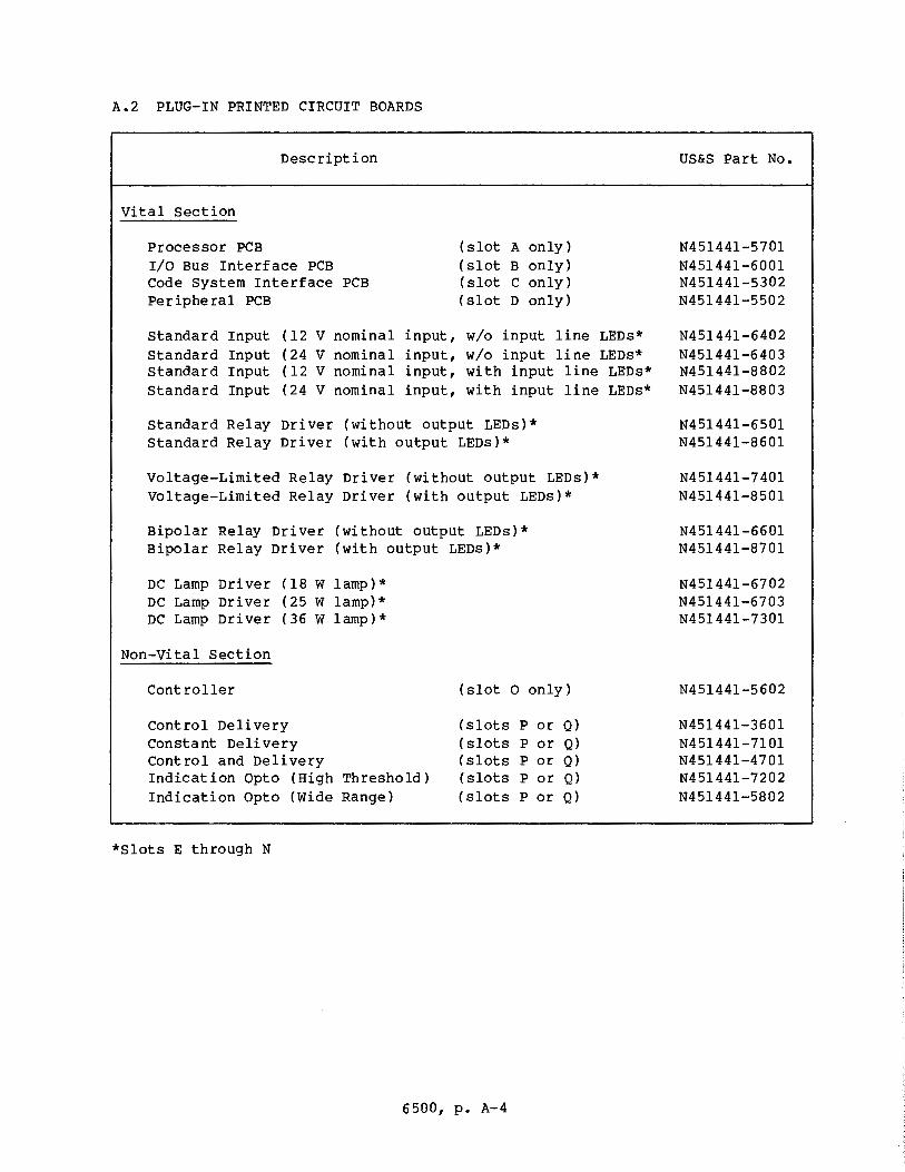
A.2 PLUG-IN PRINTED CIRCUIT BOARDS
Description
Vital Section
Processor PCB I/0 Bus Interface PCB Code System Interface PCB Peripheral PCB
Standard Input Standard Input Standard Input Standard Input
(12 (24 (12 (24
V nominal v nominal v nominal v nominal
input, input, input, input,
( slot A only) (slot B only) ( slot C only) (slot D only)
w/o input line LEDs* w/o input line LEDs* with input line LEDs* with input line LEDs*
Standard Relay Driver (without output LEDs)* Standard Relay Driver (with output LEDs)*
Voltage-Limited Relay Driver (without output LEDs)* Voltage-Limited Relay Driver (with output LEDs)*
Bipolar Relay Driver (without output LEDs)* Bipolar Relay Driver (with output LEDs)*
DC Lamp Driver (18 W lamp)* DC Lamp Driver (25 W lamp)* DC Lamp Driver (36 W lamp)*
Non-Vital Section
Controller ( slot O only)
Control Delivery Constant Delivery Control and Delivery Indication Opto (High Threshold) Indication Opto (Wide Range)
*Slots E through N
(slots (slots (slots (slots (slots
6500, p. A-4
P or Q) P or Q) p or Q) p or Q) p or Q)
US&S Part No.
N451441-5701 N451441-6001 N451441-5302 N451441-5502
N451441-6402 N451441-6403 N451441-8802 N451441-8803
N451441-6501 N451441-8601
N451441-7401 N451441-8501
N451441-6601 N451441-8701
N451441-6702 N451441-6703 N451441-7301
N451441-5602
N451441-3601 N451441-7101 N451441-4701 N451441-7202 N451441-5802
A.3 VITAL SECTION SERIAL LINK CABLE ASSEMBLIES
A.3.1 Complete Assemblies
Description
MICROLOK PLUS Vital Master Port (EIA RS-423) to: External MICROLOK PLUS Satellite Port or, External MICROLOK Satellite Port
MICROLOK PLUS Vital Master Port to Modem (EIA RS-423)
MICROLOK PLUS Vital Satellite Port to Modem (EIA RS-423)
MICROLOK PLUS Code System Port (EIA RS-423) to: External MICROLOK PLUS Non-Vital Controller or, External GENISYS Non-Vital Controller or, Intra-Unit*
Length
10 ft. 15 ft. 25 ft. 35 ft.
2.5 ft. 5 ft.
10 ft. 15 ft. 20 ft.
US&S Part No.
N451458-8201 N451458-8202 N451458-8203 N451458-8204
N451458-8301
N451458-8001
N451458-9801* N451458-9802 N451458-9803 N451458-9804 N451458-9805
*Used for intra-unit connection between vital Code System and non-vital Controller PCBs.
6500, p. A-5
A.3.2 Standard Components
A.3.2.1 37-Pin D Connector/Cable Assemblies (Master/Satellite)
The MICROLOK PLUS vital CPU uses the same serial data cable assemblies as the MICROLOK system, except for the code system interface. For standard parts lists, refer to:
Subject
37-Pin "D" Connector to MICROLOK PLUS Vital Master Port - Parts List
37-Pin "D" Connector to MICROLOK PLUS Vital Satellite Port -Parts List
Cross Reference
SM-64008, section A.2.2.1, page A-5
SM-6400B, section A.2.2.2, page A-6
NOTE
Refer to section 2.9.4 of this manual for application of the VCOR drive wires.
6500, p. A-6
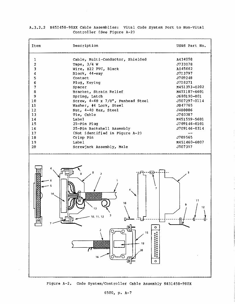
A.3.2.2 N451458-98XX Cable Assemblies: Vital Code System Port to Non-Vital Controller (See Figure A-2)
Item
1 2 3 4 5 6 7 8 9
10 11 12 13 14 15 16 17 18 19 20
4
7
Description
Cable, Multi-Conductor, Shielded Tape, 3/4 W Wire, #22 PVC, Black Block, 44-way contact Plug, Keying Spacer Bracket, Strain Relief Spring, Latch Screw, 4-40 x 7/s•, Panhead Steel Washer, #4 Lock, Steel Nut, 4-40 Hex, Steel Tie, Cable Label 25-Pin Plug 25-Pin Backshell Assembly (Not identified in Figure A-2) Crimp Pin Label Screwjack Assembly, Male
---El--
\ 4 7
""' 10
i_ __ 0
2 15 0
Oo Oo Oo Oo Oo Oo Oo Oo Oo Oo Oo Oo
0
US&S Part No.
A434058 J733078 A045662 J713797 J709248 J718271 M451393-0202 M451187-6601 J680190-001 J507297-0114 J047765 J480006 J7 0338 7 M451559-5601 J709146-0101 J709146-0314
J709565 M451460-6007 J507357
3
11
-- -1}---j-~ I"
Figure A-2. Code System/Controller Cable Assembly N451458-980X
6500, p. A-7
A.4 VITAL SECTION LOCAL I/0 CABLE ASSEMBLIES
The MICROLOK PLUS vital I/0 section uses the same connector/cable assemblies as the MICROLOK system. For top assemblies and standard parts lists, refer to:
Subject
Vital I/0 Connectors - Parts Lists
Cross Reference
SM-6400C, section A.2.6, page A-18
NOTE
Add the following connector/cable assembly top part number to the listing in SM-6400C:
Voltage Limited Output Cable - N451458-6702
The tag (item 11) for this assembly is as follows:
Tag, "Voltage-Limited Outputs" - M451640-3906
A.5. NON-VITAL SECTION SERIAL AND LOCAL CABLE ASSEMBLIES
The MICROLOK PLUS non-vital section uses the same connector/cable assembly as the GENISYS system. For standard parts lists, refer to:
Subject
Non-Vital Serial and Local Connector Assembly - Parts List
Cross Reference
SM-6300B, section 2.5.2.2, page 2-11 (Figure 2-2)
A.6 DEVELOPMENT SYSTEM HARDWARE AND SOFTWARE
The MICROLOK PLUS vital CPU uses the same development system equipment as the MICROLOK system. For standard parts lists, refer to:
Subject
MICROLOK Development System, Hardware and Software Part Lists
Cross Reference
SM-6400A, Appendix A, page A-1
The MICROLOK PLUS non-vital Controller uses the same development system equipment as the GENISYS system. For standard parts lists, refer to:
Subject
GENISYS Development System, Hardware and Software Part Lists
Cross Reference
SM-6300A, Appendix A, page A-1
6500, p. A-8
lc::<]UNION SWITCH 1UJ& SIGNAL INC. A· member of the ANSALDO Group 5800 Corporate Drive Pittsburgh, PA 15237
SERVICE MANUAL 6500
APPENDIX B
KEY COMPARISONS OF:
MICROLOK PLUS TM
VITAL PLUS NON-VITAL CONTROL PACKAGE
September, 1990 A-09/90-100-2882-1 100280F
MICROLOK R
VITAL INTERLOCKING CONTROL SYSTEM
GENISYSR NON-VITAL LOGIC EMULATOR
COPYRIGHT 1990, UNION SWITCH & SIGNAL INC. PRINTED IN USA
AN SAL DO Trasporti

°' u, 0 0 ... -a . 0, I
f--0
COMPONENT OR FUNCTION MICROLOK PLUS
Cardfile Single cardfile - 17 slots:
card Slot Numbering
PCB Arrangements
P• B-1
Vital CPU: A through D
Vital I/0: E through N
Non-Vital Control: 0 Non-Vital I/0: P and Q
Vital CPU: Fixed Locations 3 or 4 PCBs Code System PCB optional
Vital I/0: - Up to 10 PCBs - Output PCBs left of input
PCBs - No empty slot(s) between
PCBs
Non-Vital Controller: Fixed location
Non-Vital I/0: - 1 or 2 PCBs - Output PCB left of
input PCB
MICROLOK
CPU cardfile - 16 slots I/0 Cardfile - 15 slots
CPU: Jl through Jl6 (JS to Jl2 active)
I/0 Jl through Jl5
----
CPU: - Variable locations - 8 slots active - 1 or 2 CPUs - 3 or 4 PCBs per CPU - Code System PCB optional
I/0: - Up to 15 PCBs - Output PCBs left of input
PCBs - No empty slot(s) between
PCBs
GENISYS
Single cardfile, 18 slots
Controller: J2 I/0: J3 through Jl8
- Power Supply - fixed location
- Controller - fixed location - Up to 16 non-vital I/0 PCBs - Output PCBs left of input
PCBs - Empty slot(s) between PCBs
permitted
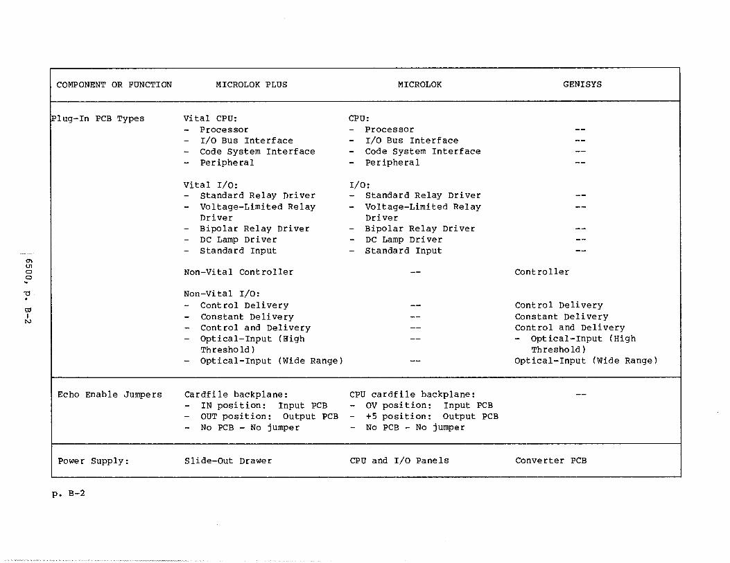
°' U1 0 0 ..
'Cl . tel I
[',.)
COMPONENT OR FUNCTION
Plug-In PCB Types
Echo Enable Jumpers
Power Supply:
P• B-2
MICROLOK PLUS
Vital CPU: - Processor - I/0 Bus Interface - Code System Interface - Peripheral
Vital I/0: - standard Relay Driver - Voltage-Limited Relay
Driver - Bipolar Relay Driver - DC Lamp Driver - standard Input
Non-Vital Controller
Non-Vital I/0: - Control Delivery - Constant Delivery - Control and Delivery - Optical-Input (High
Threshold) - Optical-Input (Wide Range)
Cardfile backplane: - IN position: Input PCB - OUT position: Output PCB - No PCB - No jumper
Slide-Out Drawer
MICROLOK
CPU: - Processor - I/0 Bus Interface - Code System Interface - Peripheral
I/0: - Standard Relay Driver - Voltage-Limited Relay
Driver - Bipolar Relay Driver - DC Lamp Driver - Standard Input
CPU cardfile backplane: - OV position: Input PCB - +5 position: Output PCB - No PCB - No jumper
CPU and I/0 Panels
GENISYS
Controller
Control Delivery Constant Delivery Control and Delivery - Optical-Input (High
Threshold) Optical-Input (Wide Range)
Converter PCB
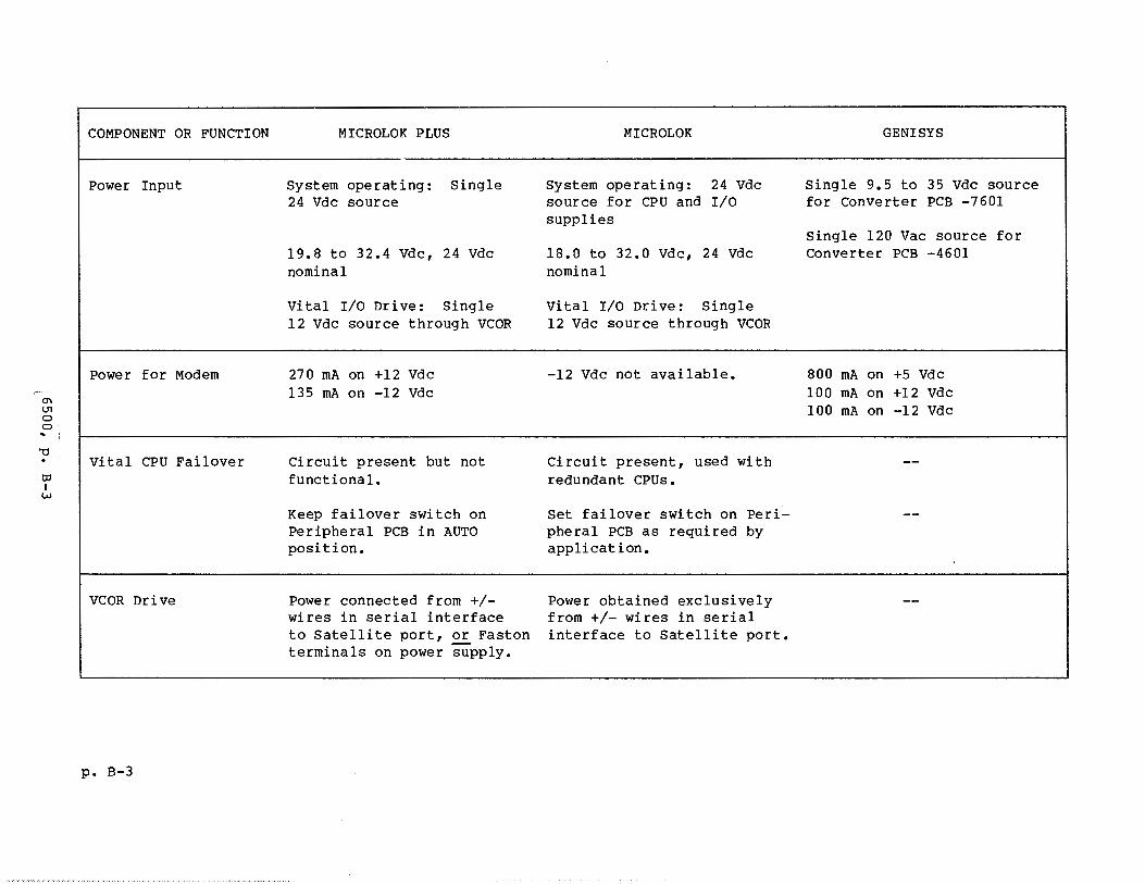
°' (.11
0 0 ..
'O . 0, I w
COMPONENT OR FUNCTION
Power Input
Power for Modem
Vital CPU Failover
VCOR Drive
P• B-3
MICROLOK PLUS
System operating: Single 24 Vdc source
19.8 to 32.4 Vdc, 24 Vdc nominal
Vital I/0 Drive: Single 12 Vdc source through VCOR
270 mA on +12 Vdc 135 mA on -12 Vdc
Circuit present but not functional.
Keep failover switch on Peripheral PCB in AUTO position.
Power connected from+/wires in serial interface to Satellite port, or Faston terminals on power supply.
MICROLOK
System operating: 24 Vdc source for CPU and I/0 supplies
18.0 to 32.0 Vdc, 24 Vdc nominal
Vital I/0 Drive: Single 12 Vdc source through VCOR
-12 Vdc not available.
Circuit present, used with redundant CPUs.
Set failover switch on Peripheral PCB as required by application.
Power obtained exclusively from+/- wires in serial interface to Satellite port.
GENISYS
Single 9.5 to 35 Vdc source for Converter PCB -7601
Single 120 Vac source for Converter PCB -4601
800 mA on +5 Vdc 100 mA on +12 Vdc 100 mA on -12 Vdc
O'\ U1 0 0 .. 'U . ttJ I
""'
COMPONENT OR FUNCTION MICROLOK PLUS
Serial Interfaces Vital CPU, Master and Satellite Ports:
37-pin "D" EIA RS-423 No redundant CPUs
MICROLOK
CPU, Master and Satellite Ports:
37-pin "D" EIA RS-423 Redundant CPU options
Vital CPU, Code System port: CPU, Code System Port: - 25-pin "D" - EIA RS-423 - No redundant CPUs
Non-Vital Controller port: - 44-pin PCB edge connector - EIA RS-423 or sv TTL - No redundant CPUs
Current Loop Communi- Via optional Serial Comm • cations Adapter panel:
P• B-4
- Separate external power supply required.
- Use for vital or nonvital communications.
- 37-pin "D" - EIA RS-423 or sv TTL - Redundant CPU option
Via optional Serial Comm. Adapter panel: - Power can be obtained
from CPU or I/0 power supplies.
GENISYS
Controller PCB Port: - 44-pin PCB edge connector - EIA RS-423 or sv TTL - No redundant CPUs
°' V1 0 0 ...
'? 01 I
V1
COMPONENT OR FUNCTION
Application Logic
Executive Software
P• B-5
MICROLOK PLUS
Vital Section: Uses MICROLOK Development System Maximum I/0 boards specified: 10
Non-Vital Section: Uses GENISYS Development System Maximum I/0 boards specified: 2
Vital CPU: Revision 8 and higher
MICROLOK
CPU: Uses MICROLOK Development System Maximum I/0 boards specified: 15
CPU: Revisions 1 through 8 and higher as determined by delivery date.
Code System: higher
Revision 3 and Code System: Revisions 1 through 3 and higher, as determined by delivery date.
Non-Vital Controller: Revision 9
GENISYS
Controller Uses GENISYS Development system Maximum I/0 boards specified: 16
Controller: Revisions 1 through 9 and higher as determined by delivery date.