Embed Size (px)
Citation preview

1 of 27
Rafael J. Betancourt ZamoraCenter for Integrated Systems
Department of Electrical EngineeringStanford University
ABabcdfghiejkl
October 29, 1997
A Low Power Frequency Synthesizer for Wireless
Biotelemetry
2 of 27
A Low Power Frequency Synthesizer for Wireless Biotelemetry
Rafael J. Betancourt Zamora • Center for Integrated Systems • Department of Electrical Engineering • Stanford University
ABabcdfghiejkl Outline
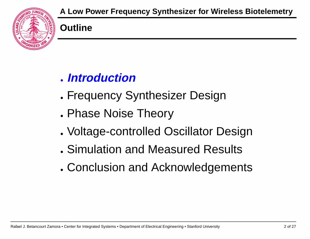
• Introduction• Frequency Synthesizer Design
• Phase Noise Theory
• Voltage-controlled Oscillator Design
• Simulation and Measured Results
• Conclusion and Acknowledgements

3 of 27
A Low Power Frequency Synthesizer for Wireless Biotelemetry
Rafael J. Betancourt Zamora • Center for Integrated Systems • Department of Electrical Engineering • Stanford University
ABabcdfghiejkl Biotelemetry is Crucial for Space Life Sciences
• On the ground, animals can be housed separately for data collection, and tethered systems are feasible. In space, where volume is very costly, animals must be group-housed, making tethers undesirable.
• In vivo experiments often require anesthetized animals and hard-wired connections to the implant, creating a risk of infection due to transcutaneous leads.
• NASA-Ames Research Center is developing the Advanced BioTelemetry System (ABTS) to conduct space-based animal research.
• Implantable biotelemetry supports real-time data gathering. It allows experiments with awake and unrestrained animals, and eliminates problems with lead breakage, movement artifacts, and ground loops.
• NASA needs a low power implantable transmitter that can relay biosensor data using the 174-216MHz band.

4 of 27
A Low Power Frequency Synthesizer for Wireless Biotelemetry
Rafael J. Betancourt Zamora • Center for Integrated Systems • Department of Electrical Engineering • Stanford University
ABabcdfghiejkl Human Applications for Biotelemetry
• NASA researchers are collaborating with doctors at the University of California-San Francisco's (UCSF) Fetal Treatment Center to adapt space biosensor and biotelemetry technology for the monitoring of fetuses with life-threatening congenital conditions.
• At UCSF’s Fetal Treatment Center there is a need for telemetry of physiological parameters of human fetuses for monitoring and identifying distress after surgery.
• A telemetry implant that will monitor heart rate, temperature, pH, and amniotic fluid pressure is required to operate in utero for up to 3 months.

5 of 27
A Low Power Frequency Synthesizer for Wireless Biotelemetry
Rafael J. Betancourt Zamora • Center for Integrated Systems • Department of Electrical Engineering • Stanford University
ABabcdfghiejkl200MHz
Fre q uenc ySynthesizer
QPSKModulator
I Q
DATA
Power &Control
RFAm p
Goal: An Implantable Biotelemetry Transmitter
• Frequency: 174-216MHz
• Data Rate: 100 kbps
• Modulation: Quadrature Phase Shift Keying (QPSK)
• Range: 1 meter
• Power source: 3.6 V, 750mAH lithium
• Implant lifetime: 100 hours (continuous)
• Implant volume: 5 cm3 (including battery)
• Our goal is to design and build a low-power radio transmitter in CMOS suitable for short range biosensor and implantable use.

6 of 27
A Low Power Frequency Synthesizer for Wireless Biotelemetry
Rafael J. Betancourt Zamora • Center for Integrated Systems • Department of Electrical Engineering • Stanford University
ABabcdfghiejkl Outline
• Introduction
• Frequency Synthesizer Design
• Phase Noise Theory
• Voltage-controlled Oscillator Design
• Simulation and Measured Results
• Conclusion and Acknowledgements

7 of 27
A Low Power Frequency Synthesizer for Wireless Biotelemetry
Rafael J. Betancourt Zamora • Center for Integrated Systems • Department of Electrical Engineering • Stanford University
ABabcdfghiejklFrequenc y
PhaseDetector
Frequenc yPhase
Detector
Char g e Pum p& Loo p Filter
Rin gVCO
Divide-b y -2
Pro g rammableDivider
UP
DOWN
FREF
FOUT
2µA 10µA
800µA
50µA
240µA
• The most important parameter of an implanted biotelemetry system is power dissipation.
• A significant portion of the power budget is allocated to the generation of the RF carrier.
• Traditionally, frequency synthesizers have been implemented using phase-locked loops (PLLs).
• The major sources of power dissipation are the VCO (73%) and the frequency divider (22%).
Phase-locked Loop Frequency Synthesizer
Power budget for a typical CMOS PLL frequency synthesizer used in microprocessor clock generation 1.
1V. Kaenel, et al., “A 320MHz, 1.5mW at 1.35V CMOS PLL for Microprocessor Clock Generation", Intl. Solid-State Circuits Conference, Feb. 1996, pp.132-133.

8 of 27
A Low Power Frequency Synthesizer for Wireless Biotelemetry
Rafael J. Betancourt Zamora • Center for Integrated Systems • Department of Electrical Engineering • Stanford University
ABabcdfghiejklLoo p Filter
Rin gVCO
FREF
FOUT
Fre q uenc yPhase
Detector
DifferentialFrequenc y
Discriminator
VD
VC
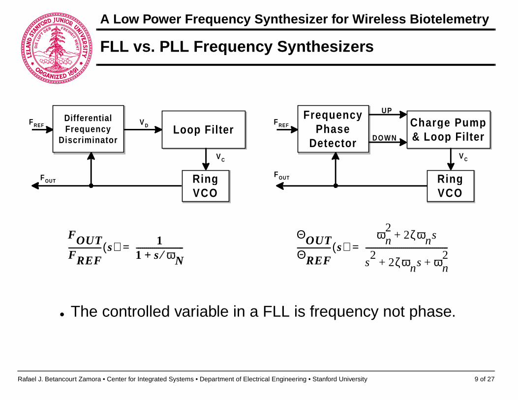
• A linear analysis using a single pole filter shows that this is a first order system, and thus inherently stable (neglecting sampled-data effects).
Frequency-locked Loop Frequency Synthesizer
LF s( ) 1sC------=
FOUT s( ) KV VC s( )⋅=
VD s( ) KD FREF FOUT–( )⋅=
FOUTFREF----------------- s( ) 1
1 s ωN⁄+------------------------= ωN
KV KD⋅
C---------------------=
• Closed loop response: • where ωΝ (rad/s) is the loop bandwidth
9 of 27
A Low Power Frequency Synthesizer for Wireless Biotelemetry
Rafael J. Betancourt Zamora • Center for Integrated Systems • Department of Electrical Engineering • Stanford University
ABabcdfghiejklLoo p Filter
Rin gVCO
FREF
FOUT
Fre q uenc yPhase
Detector
DifferentialFrequenc y
Discriminator
VD
VC
Fre q uenc yPhase
Detector
Fre q uenc yPhase
Detector
Char g e Pum p& Loo p Filter
Rin gVCO
UP
DOWN
FREF
FOUT
VC
FLL vs. PLL Frequency Synthesizers
ΘOUTΘREF----------------- s( )
ωn2
2ζωns+
s2
2ζωns ωn2
+ +------------------------------------------=
• The controlled variable in a FLL is frequency not phase.
FOUTFREF----------------- s( ) 1
1 s ωN⁄+------------------------=

10 of 27
A Low Power Frequency Synthesizer for Wireless Biotelemetry
Rafael J. Betancourt Zamora • Center for Integrated Systems • Department of Electrical Engineering • Stanford University
ABabcdfghiejklV C O
F REF
LF
D F D
C 1
C 2
F O U T
• This FLL does not require a frequency divider, which represents 22% of the power budget for the PLL example just shown.
• The FLL can perform frequency comparison directly without a divider by using a DFD implemented with switched capacitor circuits.
• The output frequency is determined by the capacitor ratio, C1/C2, and the reference frequency.
Differential Frequency Discriminator
FOUT FREF
C1C2-------
⋅=

11 of 27
A Low Power Frequency Synthesizer for Wireless Biotelemetry
Rafael J. Betancourt Zamora • Center for Integrated Systems • Department of Electrical Engineering • Stanford University
ABabcdfghiejkl• In a synthesizer application, the reference frequency source
is usually a crystal oscillator with very low phase noise.
• A PLL tracks the phase noise of the reference signal, relaxing the close-in phase noise requirements of the VCO.
• However, a FLL tracks the VCO’s frequency, not phase, forcing more stringent requirements on the VCO.
• The VCO’s power dissipation is determined by the frequency of operation and the phase noise performance required.
• In biotelemetry, data rates are low (10-100kbps), and channel spacing wide (3MHz), relaxing the phase noise requirements for the VCO.
Power Dissipation vs. Phase Noise

12 of 27
A Low Power Frequency Synthesizer for Wireless Biotelemetry
Rafael J. Betancourt Zamora • Center for Integrated Systems • Department of Electrical Engineering • Stanford University
ABabcdfghiejkl Outline
• Introduction
• Frequency Synthesizer Design
• Phase Noise Theory
• Voltage-controlled Oscillator Design
• Simulation and Measured Results
• Conclusion and Acknowledgements
13 of 27
A Low Power Frequency Synthesizer for Wireless Biotelemetry
Rafael J. Betancourt Zamora • Center for Integrated Systems • Department of Electrical Engineering • Stanford University
ABabcdfghiejkl
fo + ∆f
L ∆f( )
1
f3----
1
f2----
Noise Floor
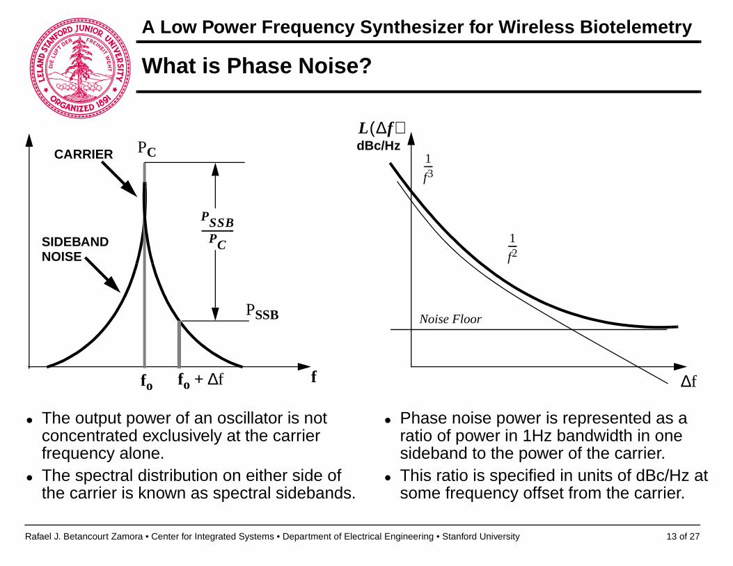
What is Phase Noise?
fo
SIDEBAND NOISE
CARRIER
• The output power of an oscillator is not concentrated exclusively at the carrier frequency alone.
• The spectral distribution on either side of the carrier is known as spectral sidebands.
PC
∆f f
PSSB
PSSBPC
---------------
• Phase noise power is represented as a ratio of power in 1Hz bandwidth in one sideband to the power of the carrier.
• This ratio is specified in units of dBc/Hz at some frequency offset from the carrier.
dBc/Hz

14 of 27
A Low Power Frequency Synthesizer for Wireless Biotelemetry
Rafael J. Betancourt Zamora • Center for Integrated Systems • Department of Electrical Engineering • Stanford University
ABabcdfghiejklt
Vout
t
Vout
∆V
∆V
Oscillators are Time-Variant Systems
• A current impulse injected at the peak only changes the amplitude and has no effect on the phase.
• A current impulse injected at the zero-crossing only changes the phase and has minimal effect on the amplitude.
hφ t τ,( )Γ ω0τ( )
qmax-------------------u t τ–( )=
• where the Impulse Sensitivity Function Γ(x) is a periodic function.
• and qmax is the maximum charge displacement in the tank.
C Li(t)

15 of 27
A Low Power Frequency Synthesizer for Wireless Biotelemetry
Rafael J. Betancourt Zamora • Center for Integrated Systems • Department of Electrical Engineering • Stanford University
ABabcdfghiejkl Impulse Sensitivity Function for Ring Oscillators
t
Vout t( )
t
Γ ωt( )
• Γ(x) can be calculated directly from the waveform.
• Since Γ(x) is periodic, it may be expressed as a Fourier series, and used in a superposition integral to determine the phase noise spectrum resulting from known device and circuit noise1.
1T. Lee, "CMOS RF: No Longer an Oxymoron", IEEE GaAs IC Symp., Oct. 1997, pp.244-247.
φ t( ) 1qmax--------------
c02----- i τ( )dτ
∞–
t
∫ cn in τ( ) nωτ( )cos dτ∞–
t
∫n 1=
∞∑+=

16 of 27
A Low Power Frequency Synthesizer for Wireless Biotelemetry
Rafael J. Betancourt Zamora • Center for Integrated Systems • Department of Electrical Engineering • Stanford University
ABabcdfghiejklc0
c1c2
c3
2f0f0 3f0f
f
N f( ) 1f--- Noise
2f0f0 3f0f
Upconversion of Device 1/f Noise
• Phase noise close to the carrier results from the folding of device noise centered at integer multiples of the carrier frequency.
• The upconversion of device 1/f noise occurs through c0, the DC value of the ISF.
• The DC value of the ISF is governed by the symmetry properties of the waveform.

17 of 27
A Low Power Frequency Synthesizer for Wireless Biotelemetry
Rafael J. Betancourt Zamora • Center for Integrated Systems • Department of Electrical Engineering • Stanford University
ABabcdfghiejkl Hajimiri Phase Noise Model 2
2A. Hajimiri, T. Lee, "A General Theory of Phase Noise in Oscillators", IEEE Journal of Solid-State Circuits (in press).
L ∆ω{ } 10ΓRMS
2
qmax2
-----------------in2 ∆f⁄
4∆ω2---------------⋅
log⋅=
• Phase Noise in 1/f2 region is due to device thermal noise.
• Phase Noise in 1/f3 region is due to device 1/f noise.
• It is commonly assumed that the 1/f3 corner of phase noise is the same as the 1/f corner of the device noise spectrum.This is NOT the case.
ω1 f
3⁄ω1 f⁄
c0c1-----
2
⋅≈
f
Sφ f( )
1
f2----
c0
c1
ω1 f⁄ω
1 f3⁄
1
f3----
18 of 27
A Low Power Frequency Synthesizer for Wireless Biotelemetry
Rafael J. Betancourt Zamora • Center for Integrated Systems • Department of Electrical Engineering • Stanford University
ABabcdfghiejkl Outline
• Introduction
• Frequency Synthesizer Design
• Phase Noise Theory
• Voltage-controlled Oscillator Design
• Simulation and Measured Results
• Conclusion and Acknowledgements

19 of 27
A Low Power Frequency Synthesizer for Wireless Biotelemetry
Rafael J. Betancourt Zamora • Center for Integrated Systems • Department of Electrical Engineering • Stanford University
ABabcdfghiejkl
• The VCO design is critical in the performance of the FLL synthesizer as the phase noise at the output of the FLL is solely a function of the phase noise of the VCO.
• The VCO consists of a 4-stage differential ring oscillator3.
• Frequency control is achieved by changing the biasing of the buffer stages which determines the delay through each cell.
Voltage-controlled Oscillator Design
3 A.W. Buchwald, K.W.Martin, "High Speed Voltage Controlled Oscillators with Quadrature Outputs", Electronics Letters, 14 Feb. 1991, Vol. 27 No. 4, pp.309-310.

20 of 27
A Low Power Frequency Synthesizer for Wireless Biotelemetry
Rafael J. Betancourt Zamora • Center for Integrated Systems • Department of Electrical Engineering • Stanford University
ABabcdfghiejkl Differential Delay Buffer Design
• The differential buffers used have been shown to have excellent noise and power supply rejection characteristics4.
• The layout of the ring oscillator is symmetrical and load balanced to avoid any skewing between the phases.
4 M. Horowitz, et al., "PLL Design for a 500MB/s Interface", Intl. Solid-State Circuits Conference, Feb. 1993, pp.160-161.
VCO BIAS
DECODER
MODULATOR BIAS
30µm
Vctl
inp
outm
inm
outp
Vpbias
Vnbias
Vdd

21 of 27
A Low Power Frequency Synthesizer for Wireless Biotelemetry
Rafael J. Betancourt Zamora • Center for Integrated Systems • Department of Electrical Engineering • Stanford University
ABabcdfghiejkl
• IDD is the tail current of a single stage
• EC is the critical field (e.g., 4.918 V/µm)
• LEFF is the gate length of the differential-pair devices (e.g., 0.5µm)
• We selected the 100µA curve, for a total current drain of 500µA at 200MHz.
Phase Noise Analysis of Ring Oscillator VCO
L ∆ω{ } 1064kT
IDDECLEFF-----------------------------------
fo2
∆ω2-----------
log⋅=
Single-sideband phase noise (dBc/Hz) for a differential ring oscillator in the 1/f2 region
104
105
106
−140
−120
−100
−80
−60
−40
Offset Frequency, Hz
Pha
se N
oise
, dB
c/H
z
Single−sideband Phase Noise Spectral Density
10uA
100uA
1000uA

22 of 27
A Low Power Frequency Synthesizer for Wireless Biotelemetry
Rafael J. Betancourt Zamora • Center for Integrated Systems • Department of Electrical Engineering • Stanford University
ABabcdfghiejkl Outline
• Introduction
• Frequency Synthesizer Design
• Phase Noise Theory
• Voltage-controlled Oscillator Design
• Simulation and Measured Results
• Conclusion and Acknowledgements

23 of 27
A Low Power Frequency Synthesizer for Wireless Biotelemetry
Rafael J. Betancourt Zamora • Center for Integrated Systems • Department of Electrical Engineering • Stanford University
ABabcdfghiejkl
0.8 0.9 1 1.1 1.2 1.3 1.4 1.550
100
150
200
250
300
350
Control Voltage, V
Out
put F
requ
ency
, MH
z
VCO Voltage−to−Frequency Transfer Characteristic
3.0V
2.7V
1.8V
Test Results: VCO Transfer Characteristic
• Fabricated through MOSIS using the HP 0.5µm CMOS process.
• The VCO voltage-to-frequency transfer characteristic was measured for different supply voltages.
• Tuning Range: 350kHz-707MHz @3V
• VCO Gain = 321MHz/V @3V

24 of 27
A Low Power Frequency Synthesizer for Wireless Biotelemetry
Rafael J. Betancourt Zamora • Center for Integrated Systems • Department of Electrical Engineering • Stanford University
ABabcdfghiejkl• Using an HP8590B
spectrum analyzer, the phase noise was measured at -82dBc/Hz for 100kHz offset from a 200MHz carrier.
• These measurements are within 2dB of the predicted values for frequency offsets between 10Hz and 1MHz.
Test results using RDI’s NTS-1000A phase noise measurement test set, along with the theoretical phase noise performance predicted by the Hajimiri model (fc=150.9MHz).
Test Results: Phase Noise
101
102
103
104
105
106
−150
−100
−50
0
50
Offset Frequency, Hz
Pha
se N
oise
, dB
c/H
z
Single−sideband Phase Noise Spectral Density
measuredtheory

25 of 27
A Low Power Frequency Synthesizer for Wireless Biotelemetry
Rafael J. Betancourt Zamora • Center for Integrated Systems • Department of Electrical Engineering • Stanford University
ABabcdfghiejkl Outline
• Introduction
• Frequency Synthesizer Design
• Phase Noise Theory
• Voltage-controlled Oscillator Design
• Simulation and Measured Results
• Conclusion and Acknowledgements

26 of 27
A Low Power Frequency Synthesizer for Wireless Biotelemetry
Rafael J. Betancourt Zamora • Center for Integrated Systems • Department of Electrical Engineering • Stanford University
ABabcdfghiejkl
• The frequency-locked loop (FLL) synthesizer imposes more stringent phase noise requirements on the VCO.
• A design technique using the Hajimiri phase noise model was presented.
• A 200MHz ring oscillator VCO was designed and fabricated in 0.5µm CMOS.
• Measurements of phase noise show good agreement with the theory.
Conclusions
Loo p Filter
Rin gVCO
FREF
FOUT
Fre q uenc yPhase
Detector
DifferentialFrequenc y
Discriminator
VD
VC20µA
500µA

27 of 27
A Low Power Frequency Synthesizer for Wireless Biotelemetry
Rafael J. Betancourt Zamora • Center for Integrated Systems • Department of Electrical Engineering • Stanford University
ABabcdfghiejkl• This work was partially supported by NASA-Ames
Research Center through a Training Grant No. NGT 2-52211.
• We gratefully acknowledge the support of John W. Hines, manager of the Sensors 2000! program at NASA-Ames Research Center.
Acknowledgements