Embed Size (px)
DESCRIPTION
A Low-Power Analog Bus for On-Chip Digital Communication Master’s Thesis Defense Farah Naz Taher Thesis Advisor: Dr. Vishwani D. Agrawal Committee Members: Dr. Victor P. Nelson, Dr. Adit D. Singh. June 21, 2013. Outline. Motivation Background Problem Statement Concept Result - PowerPoint PPT Presentation
Citation preview

A Low-Power Analog Bus for On-Chip Digital Communication
Master’s Thesis DefenseFarah Naz Taher
Thesis Advisor: Dr. Vishwani D. AgrawalCommittee Members:
Dr. Victor P. Nelson, Dr. Adit D. Singh
June 21, 2013

Outline
Motivation
Background
Problem Statement
Concept
Result
Future Work
Reference
2 April 19, 2023Farah Naz Taher
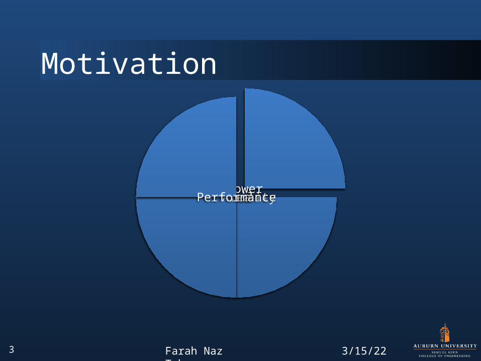
Motivation
3 April 19, 2023Farah Naz Taher
Power
TestabilityArea
Performance

Motivation• Moore’s Law: Empirical observation that component density
and performance of integrated circuits doubles every year
4 April 19, 2023Farah Naz Taher
G. E. Moore, 1965S. E. Thompson et. al., Materials Today 2006.

Motivation• Pollack's Rule: Each technology generation doubles the
number of transistor on a chip which enables that performance increase is roughly proportional to square root of increase in complexity.
5 April 19, 2023Farah Naz Taher
S. Borkar, DAC 2007

Motivation
More Transistors
More Blocks
More Cores
More on-chip Communication More Power
6 April 19, 2023Farah Naz Taher

Outline
Motivation
Background
Problem Statement
Concept
Result
Future Work
Reference
7 April 19, 2023Farah Naz Taher

Bus Structure
8 April 19, 2023Farah Naz Taher
• A bus is a collection of signals (wires) that connects one or more IP components for the purpose of data communication.

Issues With Parallel Bus
• Power Dissipation
• Routing Complexity
• Area
• Signal Integrity and Crosstalk
• Performance
9 April 19, 2023Farah Naz Taher

Dynamic Power
• For low swing signaling:
Average dynamic power for a single wire:
10 April 19, 2023Farah Naz Taher
DDswingDDavgdynamic .Vf.C.V.=V I=P
Weste and Harris, 2010

Dynamic Power
• If there are n-lines in the bus with similar activity, then the total power consumed by such a bus will be n-times of a single bit line
11 April 19, 2023Farah Naz Taher
n
1i
iiswing,DDibus parallel .f..V.V C=P
Weste and Harris, 2010

Dynamic Power
• Analysis shows that interconnect power can be over 50% of the dynamic power, over 90% of the interconnect power is consumed by only 10% of the interconnections
12 April 19, 2023Farah Naz Taher
n
1i
iiswing,DDibus parallel .f..V.V C=P
Weste and Harris, 2010

The SerDes Option• SerDes is a widely used technique for replacing multiple-lines on-chip
bus with a single on-chip line to achieve high speed serial communication.
• In serial bus architecture, n parallel data bits are serialized at the transmitter side. The data transfer takes place at a speed which is n times higher than the data rate of the parallel data.
• At the receiver side, the data has to be de-serialized to reproduce the n-bit parallel word.
13 April 19, 2023Farah Naz Taher
A. Kedia et. al., ISCAS 2007 N. Hatta et. al. ISPJ 2006

Disadvantages of SerDes
Increase in the number
of transitions
n times faster frequency
More Power Consumption
14 April 19, 2023Farah Naz Taher
• Encoding scheme needs to be employed to reduce power consumption. Some proposed methods are:
• Silent: Low energy transmission• LOUD: Bit ordering

Outline
Motivation
Background
Problem Statement
Concept
Result
Future Work
Reference
15 April 19, 2023Farah Naz Taher

Problem Statement
• The objective of this work is to develop a low power analog bus for on-chip communication to replace existing parallel digital bus.
16 April 19, 2023Farah Naz Taher

Outline
Motivation
Background
Problem Statement
Concept
Result
Future Work
Reference
17 April 19, 2023Farah Naz Taher

Analog Bus• Replace n wires of an n-bit digital bus carrying data
between cores with just one (or few) wire(s) carrying analog signal(s) encoded into 2n levels of voltage
• Analog bus uses digital-to-analog converter (DAC) drivers and analog-to-digital converter (ADC) receivers.
18 April 19, 2023Farah Naz Taher

Parallel Bus vs. Analog Bus
19 April 19, 2023Farah Naz Taher
n
1i
iiswing,DDibus parallel .f..V.V C=P

Parallel bus vs. Analog Bus
20 April 19, 2023Farah Naz Taher
)(.f..VC.V=P swingDDbus analog DACADC PP

Analog Bus
21 April 19, 2023Farah Naz Taher
Parallel Bus Digital Data (Volt)
1 0 1 0 0 1 0 0 1 1 0 1 1 0 0 0
1 0 0 0 0 1 1 0 0 1 1 0 1 1 0 0
1 0 1 0 0 1 0 1 0 0 0 1 0 0 1 1
1 1 0 0 1 0 0 0 1 1 0 0 1 1 0 0
Converted Analog Bus (Volt)
1.000.06
70.67 0.00
0.06
7
0.93
3
0.26
7
0.13
3
0.60
0
0.86
7
0.26
70.67
0.86
7
0.33
3
0.13
3
0.13
3

Vswing
22 April 19, 2023Farah Naz Taher

Vswing
23 April 19, 2023Farah Naz Taher
Total number of possible variations
Total possible voltage swing
Average Voltage swing
DDn
n
V2.3
12
DDnn 1)V (22
3
1
n22

Proposition
24 April 19, 2023Farah Naz Taher
• The analog bus can be used in cases where:i. Power consumed by analog bus architecture < Power consumed
by parallel bus
ii. The signal can be reproduced without any error
• The choice of resolution for substituting the number of lines in digital buses with proposed analog bus depends on two criteria.
• i. Power consumed by the ADC and DAC• ii. Noise margin of signal line

Proposition
25 April 19, 2023Farah Naz Taher
• The analog bus can be used in cases where:i. Power consumed by analog bus architecture < Power consumed
by parallel bus
ii. The signal can be reproduced without any error
• The choice of resolution for substituting the number of lines in digital buses with proposed analog bus depends on two criteria:
• i. Power consumed by the ADC and DAC• ii. Noise margin of signal line

Proposition
26 April 19, 2023Farah Naz Taher
• Corollary 1: Analog bus is effective only if the power consumed by the analog bus
architecture is less than the power consumption of the digital bus.
• Corollary 2:• To reproduce the signal in the digital bus without any error, the noise
level should be less than half of the resolution of the ADC.
)P (P )P - (P DACADCAnalogBusDigitalBus

Proposition
27 April 19, 2023Farah Naz Taher
• Corollary 1: Analog bus is effective only if the power consumed by the analog bus
architecture is less than the power consumption of the digital bus.
• Corollary 2: To reproduce the signal in the digital bus without any error, the noise
level should be less than half of the resolution of the ADC.
)P (P )P - (P DACADCAnalogBusDigitalBus

Advantages
28 April 19, 2023Farah Naz Taher
Less Number of
wires
Lower Capacitance
Lower Voltage Swing
Power Saving

Advantages
29 April 19, 2023Farah Naz Taher
Potential Savings
Power
Crosstalk
Multiple
Drivers/
Buffers
Routing Complexity
Wire Area

Outline
Motivation
Background
Problem Statement
Concept
Experimental Result
Future Work
Reference
30 April 19, 2023Farah Naz Taher
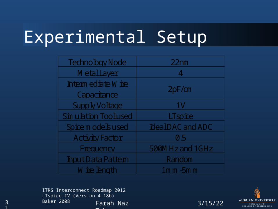
Experimental Setup
31 April 19, 2023Farah Naz Taher
Technology Node 22nmMetal Layer 4
Intermediate Wire Capacitance
2pF/cm
Supply Voltage 1VSimulation Tool used LTspice
Spice models used Ideal DAC and ADCActivity Factor 0.5
Frequency 500MHz and 1GHzInput Data Pattern Random
Wire length 1mm-5mm
ITRS Interconnect Roadmap 2012LTspice IV (Version 4.18b)Baker 2008

Replacement of 4-Line Parallel Bus
32 April 19, 2023Farah Naz Taher

Replacement of 4-Line Parallel Bus
33 April 19, 2023Farah Naz Taher
• Digital Data: Bus Input
• Analog Data: Simulated DAC Output

Replacement of 4-line Parallel Bus
34 April 19, 2023Farah Naz Taher
Bus Length Parallel Bus Analog Bus1mm 464.23µW 36.7µW2mm 928.32µW 67.2µW3mm 1.39mW 97.1µW4mm 1.85mW 126.5µW5mm 2.31mW 155.9µW
• Bus width = 4, Frequency = 1GHz

Replacement of 4-line Parallel Bus
35 April 19, 2023Farah Naz Taher
• Bus width = 4, Frequency = 1GHz
1mm 2mm 3mm 4mm 5mm0
500
1000
1500
2000
2500
Parallel Bus
Analog Bus
Bus Length
Po
wer
Co
nsu
mp
tio
n (
µW)

Replacement of 4-line Parallel Bus
36 April 19, 2023Farah Naz Taher
• Bus width = 4, Frequency = 500MHz
Bus Length Parallel Bus Analog Bus1mm 219.22µW 19.3µW2mm 438.95µW 33.73µW3mm 658.13µW 46.87µW4mm 875.34µW 59.28µW5mm 1.095mW 71.44µW

Replacement of 4-line Parallel Bus
37 April 19, 2023Farah Naz Taher
• Bus width = 4, Frequency = 500MHz
1mm 2mm 3mm 4mm 5mm0
500
1000
1500
2000
2500
Parallel Bus
Analog Bus
Bus Length
Po
wer
Co
nsu
mp
tio
n (
µW)

Replacement of 8-Line Parallel Bus
38 April 19, 2023Farah Naz Taher

Replacement of 8-Line Parallel Bus
39 April 19, 2023Farah Naz Taher
• Digital Data
• Analog Data

Replacement of 8-Line Parallel Bus
40 April 19, 2023Farah Naz Taher
• Bus width = 8, Frequency = 500MHz
Bus Length Parallel Bus Analog Bus1mm 469.8µW 19.2µW2mm 939µW 36.82µW3mm 1.4mW 54.4µW4mm 1.88mW 71.84µW5mm 2.35mW 89.2µW

Replacement of 8-Line Parallel Bus
41 April 19, 2023Farah Naz Taher
• Bus width = 8, Frequency = 500MHz
1mm 2mm 3mm 4mm 5mm0
500
1000
1500
2000
2500
Parallel Bus
Analog Bus
Bus Length
Po
wer
Co
nsu
mp
tio
n(µ
W)

Analysis for f = 500MHz
42 April 19, 2023Farah Naz Taher
Parallel Bus
Analog Bus
Power Margin
Available
Parallel Bus
Analog Bus
Power Margin
Available1mm 219.22µW 18.3µW 200.92µW 469.8µW 19.2µW 450.6 µW2mm 438.95µW 33.73µW 405.22µW 939µW 36.82µW 902.18µW3mm 658.13µW 46.87µW 611.26µW 1.4mW 54.4µW 1.345mW4mm 875.34µW 59.28µW 816.06µW 1.88mW 71.84µW 1.808mW5mm 1.095mW 71.44µW 1.023mW 2.35mW 89.2µW 2.261mW
Bus Length
4-Line Bus Power Consumption 8-Line Bus Power Consumption

Analysis
43 April 19, 2023Farah Naz Taher
• Bus Width: 4, Frequency: 500MHz, Length = 1mm• The average power consumption per mm for the analog bus is
around 16.17 µW. • The average power consumption for a 4-bit bus is 219 µW.
• Bus Width: 8, Frequency: 500MHz, Length = 1mm• The average power consumption per mm for the analog bus is
around 18.3 µW. • The average power consumption for an 8-bit bus is 469.2 µW.

Analysis
44 April 19, 2023Farah Naz Taher
• The power consumption in the parallel bus has an exponential increase with respect to the bus length whereas the power consumption in the analog bus is increasing slowly.
• SPICE simulation for an ideal case shows that, the ratio of bus power consumed by the proposed analog scheme to a typical parallel digital scheme is given by Panalog/Pdigital = 1/(3n).

Analysis
45 April 19, 2023Farah Naz Taher
• The power consumption of the ADC/DAC can be a design challenge for analog bus.
• ADC/DAC with a power consumption in µW range exists already. Example:
• ADC (ADS7924 from Texas Instruments): 5.5µW• DAC (LTC1591 from Linear technology): 10µW
• In the 4-Bit and 8-Bit cases we has an available power margin of 200µW and 450µW respectively.
• The analog bus architecture will be power beneficial even after addition of 15.5µW power consuming elements.

Outline
Motivation
Background
Problem Statement
Concept
Experimental Result
Future Work
Reference
46 April 19, 2023Farah Naz Taher

Future Work
47 April 19, 2023Farah Naz Taher
• This thesis examined the feasibility of the scheme, much work remains to be done
Design Suitable
Converters
Design Encoding Scheme
Analyze the Scheme in
Digital Testing
Fabricate the System on a Chip

Outline
Motivation
Background
Problem Statement
Concept
Experimental Result
Future Work
Reference
48 April 19, 2023Farah Naz Taher

Reference
49 April 19, 2023Farah Naz Taher
• “14-Bit and 16-Bit Parallel Low Glitch Multiplying DACs with 4-Quadrant Resistors,“ White Paper, Linear Technology Corporation, Feb. 1999. http://cds.linear.com/docs/en/datasheet/15917fa.pdf.
• “2.2V, 12-Bit, 4-Channel, microPOWER Analog-to-Digital converter With I2C Interface,“ White Paper, Texas Instruments Incorporated, Jan. 2012. http://www.ti.com/lit/ds/symlink/ads7924.pdf.
• “LTspice IV (Version 4.18b)," 2013. Linear Technology Corporation, http://www.com/designtools/software/#LTspice.• R. J. Baker, CMOS Mixed-signal Circuit Design. John Wiley & Sons, 2008.• S. Borkar, “Thousand Core Chips: A Technology Perspective," in Proc. 44th Design Automation Conference, 2007, pp.
746-749.• N. Hatta, N. D. Barli, C. Iwama, L. D. Hung, D. Tashiro, S. Sakai, and H. Tanaka, “Bus Serialization for Reducing
Power Consumption," ISPJ Trans. Advanced Computing Systems, vol. 47, no. SIG-3, pp. 686-694, Mar. 2006.• A. Kedia and R. Saleh, “Power Reduction of On-Chip Serial Links," in IEEE International Symp. Circuits and Systems,
2007, pp. 865-868.• B. Li, V. D. Agrawal, and B. Zhang, “Mixed-Signal Compression of Digital Test Data.“ Personal Communication, June
2013.• G. E. Moore, “Cramming More Components onto Integrated Circuits," Electronics. Vol. 38, no. 8, Apr. 1965.• Semiconductor Industry Association, “International Technology Roadmap for Semiconductors,“ 2012.
http://www.itrs.net/Links/2012ITRS/Home2012.htm.• F. N. Taher and V. D. Agrawal, “A Low-Power Analog Bus Approach for On-Chip Digital Communication," 31st IEEE
International Conf. Computer Design, 2013. Submitted• F. N. Taher, S. Sindia, and V. D. Agrawal, “An Analog Bus for Low Power On-Chip Digital Communication," in Work-in-
Progress Poster Session, Design Automation Conference, (Austin, Texas), June 2013.

April 19, 2023Farah Naz Taher

April 19, 2023Farah Naz Taher


![On-Chip Analog Trojan Detection Framework for ...jin.ece.ufl.edu/papers/TCAD18.pdf · A. Analog Hardware Trojans ... The transistor schematic of the A2 analog Trojan [2] circuit is](https://img.pdfslide.us/doc/110x75/5f09d7b37e708231d428c153/on-chip-analog-trojan-detection-framework-for-jineceufledupapers-a-analog.jpg)