Embed Size (px)
Citation preview
A LABVIEW BASED POWER CONVERTER DESIGN FOR TIME DOMAIN ELECTROMAGNETIC SYSTEM
HARJOT SINGH SAINI
A Thesis
in
The Department
Of
Electrical & Computer Engineering
Presented in Partial Fulfillment of the Requirements
for the Degree of Master of Applied Science
(Electrical & Computer Engineering) at
Concordia University
Montreal, Quebec, Canada
February 2014
© HARJOT SINGH SAINI, 2014
CONCORDIA UNIVERSITY SCHOOL OF GRADUATE STUDIES
This is to certify that the thesis prepared
By: Harjot Singh Saini
Entitled: “A LabVIEW based power converter design for time domain electromagnetic system” and submitted in partial fulfillment of the requirements for the degree of
Master of Applied Science
Complies with the regulations of this University and meets the accepted standards with respect to originality and quality.
Signed by the final examining committee:
________________________________________________ Chair
Dr. M. Z. Kabir
________________________________________________ Examiner, External
Dr. L. Wang (BCEE)
________________________________________________ Examiner
Dr. S. Williamson
________________________________________________ Supervisor
Dr. L. A. Lopes
Approved by: ___________________________________________
Dr. W. E. Lynch, Chair
Department of Electrical and Computer Engineering
____________20_____ ___________________________________
Dr. Christopher Trueman Interim Dean, Faculty of Engineering and
Computer Science
iii
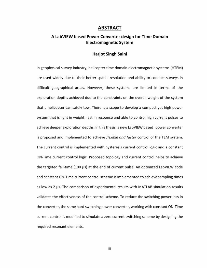
ABSTRACT
A LabVIEW based Power Converter design for Time Domain Electromagnetic System
Harjot Singh Saini
In geophysical survey industry, helicopter time domain electromagnetic systems (HTEM)
are used widely due to their better spatial resolution and ability to conduct surveys in
difficult geographical areas. However, these systems are limited in terms of the
exploration depths achieved due to the constraints on the overall weight of the system
that a helicopter can safely tow. There is a scope to develop a compact yet high power
system that is light in weight, fast in response and able to control high current pulses to
achieve deeper exploration depths. In this thesis, a new LabVIEW based power converter
is proposed and implemented to achieve flexible and faster control of the TEM system.
The current control is implemented with hysteresis current control logic and a constant
ON-Time current control logic. Proposed topology and current control helps to achieve
the targeted fall-time (100 μs) at the end of current pulse. An optimized LabVIEW code
and constant ON-Time current control scheme is implemented to achieve sampling times
as low as 2 μs. The comparison of experimental results with MATLAB simulation results
validates the effectiveness of the control scheme. To reduce the switching power loss in
the converter, the same hard switching power converter, working with constant ON-Time
current control is modified to simulate a zero current switching scheme by designing the
required resonant elements.

iv
ACKNOWLEDGEMENTS
First and foremost I would like to express my sincere gratitude to Dr. Luiz A.C. Lopes for
his invaluable guidance, ideas and motivation in my thesis work and his amazing lectures
in Power Electronics which have inspired me to continue my graduate studies in this area
of expertise. His humble attitude and helpful nature made my first steps in academic
research a fulfilling and exciting experience.
I would also like to thank Dr. Jose Martinez, a great human being and a true friend, for his
unconditional support and guidance in my research work. I deeply appreciate the way he
made my work at GDS a fun filled learning experience.
I would like to express my warm feelings of gratitude to Dr. Pragasen Pillay and Dr.
Sheldon Williamson for their time to time support and encouragement.
I am extremely grateful to my friends at Power Electronics and Energy Research (PEER)
Group at the P. D. Ziogas Laboratory for their support .I really enjoyed time to time idea
exchanges through technical discussions.
I am thankful to NSERC, Canada and Power Corporation of Canada in supporting my
studies through monetary funding.
Last but not the least thanks to the almighty God for always bestowing me with the
company of best people, in the form of family and friends who inspired my journey till
date.

v
Dedicated to my parents Sardar Mohinder Singh and Sardarni
Surinder Kaur

vi
TABLE OF CONTENTS
LIST OF FIGURES ........................................................................................................................................... viii
LIST OF TABLES ............................................................................................................................................... xi
LIST OF ACRONYMS ....................................................................................................................................... xii
LIST OF PRINCIPAL SYMBOLS ........................................................................................................................ xiii
CHAPTER 1. INTRODUCTION .......................................................................................................................... 1
1.1 AIRBORNE ELECTROMAGNETIC SYSTEMS ...................................................................................... 1
1.2 TEM SYSTEM AND PRINCIPLE ......................................................................................................... 3
1.3 THESIS OBJECTIVE AND CHALLENGES ............................................................................................ 6
1.4 THESIS CONTRIBUTIONS ................................................................................................................ 6
1.5 THESIS OUTLINE ............................................................................................................................. 7
CHAPTER 2. REVIEW OF POWER CONVERTER TOPOLOGIES IN AEM SYSTEMS ............................................... 9
2.1 INTRODUCTION .............................................................................................................................. 9
2.2 SELECTION OF CURRENT WAVEFORM ........................................................................................... 9
2.3 PRESENT CURRENT CONTROL TOPOLOGIES ................................................................................. 10
2.4 CONCLUSION ................................................................................................................................ 14
CHAPTER 3. THE PROPOSED POWER CONVERTER – DESIGN AND SIMULATIONS ........................................ 15
3.1 INTRODUCTION ............................................................................................................................ 15
3.2 IMPORTANT CONSIDERATIONS ................................................................................................... 15
3.3 PROPOSED CONVERTER TOPOLOGY ............................................................................................ 17
3.3.1 MODES OF OPERATION (HARD SWITCHING) ...................................................................... 17
3.3.2 CURRENT GOVERNING EQUATIONS .................................................................................... 20
3.3.3 SELECTION OF DC LINK CAPACITOR .................................................................................... 22
3.3.4 SELECTION OF DC POWER SOURCE ..................................................................................... 23
3.3.5 SELECTION OF IGBTS ........................................................................................................... 24
3.3.6 SIMULATION RESULTS ......................................................................................................... 25
3.4 CONSTANT ON - TIME CURRENT CONTROL SCHEME................................................................... 28
3.5 DESIGN OF SNUBBER CIRCUIT ...................................................................................................... 34
3.5.1 ADVANTAGES OF RCD SNUBBER ......................................................................................... 34
3.5.2 CALCULATION OF SNUBBER CAPACITANCE ........................................................................ 35
3.5.3 CALCULATION OF SNUBBER RESISTOR ................................................................................ 36
3.6 CONCLUSION................................................................................................................................ 37
CHAPTER 4. HARDWARE IMPLEMENTATION AND EXPERIMENTAL RESULTS ................................................ 39
4.1 INTRODUCTION ............................................................................................................................ 39
4.2 INTRODUCTION TO LABVIEW ...................................................................................................... 39
4.3 INTRODUCTION TO FPGA ............................................................................................................. 40
vii
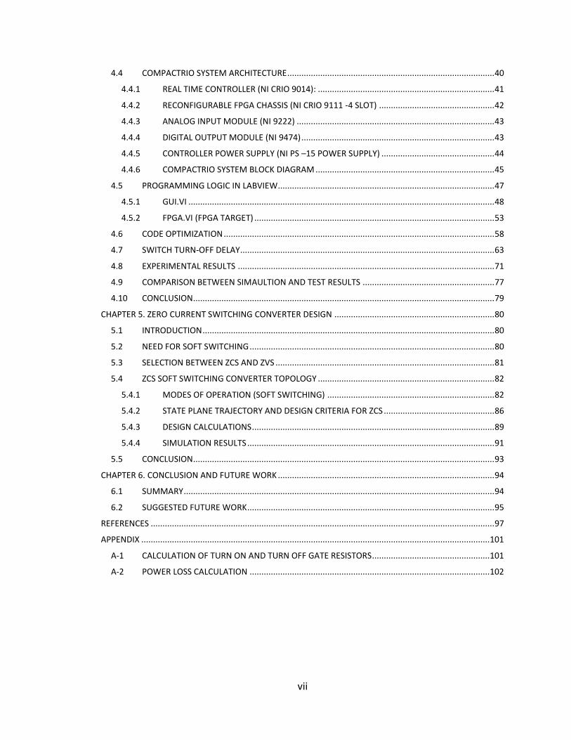
4.4 COMPACTRIO SYSTEM ARCHITECTURE ........................................................................................ 40
4.4.1 REAL TIME CONTROLLER (NI CRIO 9014): ........................................................................... 41
4.4.2 RECONFIGURABLE FPGA CHASSIS (NI CRIO 9111 -4 SLOT) ................................................. 42
4.4.3 ANALOG INPUT MODULE (NI 9222) .................................................................................... 43
4.4.4 DIGITAL OUTPUT MODULE (NI 9474) .................................................................................. 43
4.4.5 CONTROLLER POWER SUPPLY (NI PS –15 POWER SUPPLY) ................................................ 44
4.4.6 COMPACTRIO SYSTEM BLOCK DIAGRAM ............................................................................ 45
4.5 PROGRAMMING LOGIC IN LABVIEW ............................................................................................ 47
4.5.1 GUI.VI .................................................................................................................................. 48
4.5.2 FPGA.VI (FPGA TARGET) ...................................................................................................... 53
4.6 CODE OPTIMIZATION ................................................................................................................... 58
4.7 SWITCH TURN-OFF DELAY ............................................................................................................ 63
4.8 EXPERIMENTAL RESULTS ............................................................................................................. 71
4.9 COMPARISON BETWEEN SIMAULTION AND TEST RESULTS ........................................................ 77
4.10 CONCLUSION................................................................................................................................ 79
CHAPTER 5. ZERO CURRENT SWITCHING CONVERTER DESIGN .................................................................... 80
5.1 INTRODUCTION ............................................................................................................................ 80
5.2 NEED FOR SOFT SWITCHING ........................................................................................................ 80
5.3 SELECTION BETWEEN ZCS AND ZVS ............................................................................................. 81
5.4 ZCS SOFT SWITCHING CONVERTER TOPOLOGY ........................................................................... 82
5.4.1 MODES OF OPERATION (SOFT SWITCHING) ....................................................................... 82
5.4.2 STATE PLANE TRAJECTORY AND DESIGN CRITERIA FOR ZCS ............................................... 86
5.4.3 DESIGN CALCULATIONS ....................................................................................................... 89
5.4.4 SIMULATION RESULTS ......................................................................................................... 91
5.5 CONCLUSION................................................................................................................................ 93
CHAPTER 6. CONCLUSION AND FUTURE WORK ............................................................................................ 94
6.1 SUMMARY .................................................................................................................................... 94
6.2 SUGGESTED FUTURE WORK ......................................................................................................... 95
REFERENCES .................................................................................................................................................. 97
APPENDIX .................................................................................................................................................... 101
A-1 CALCULATION OF TURN ON AND TURN OFF GATE RESISTORS .................................................. 101
A-2 POWER LOSS CALCULATION ...................................................................................................... 102
viii
LIST OF FIGURES
Fig. 1.1 Fixed Wing TEM System1 .................................................................................................................... 2
Fig. 1.2 Helicopter Time Domain Electromagnetic (HTEM) system2 ............................................................... 2
Fig. 1.3 TEM Principle [4] ................................................................................................................................. 4
Fig. 1.4 TEM Waveforms ................................................................................................................................. 5
Fig. 2.1 TEM Converter Topology using two energy storage elements [7] ................................................... 10
Fig. 2.2 Load Current and capacitor voltage waveforms [7] ......................................................................... 10
Fig. 2.3 Converter Topologies for fast current reversal (a) unclamped topology (b) clamped Topology [8] 12
Fig. 2.4 Voltage and current waveforms- Unclamped Topology [8] .............................................................. 13
Fig. 3.1 Proposed Topology & Modes of Operation (Hard Switching)........................................................... 19
Fig. 3.2 Simulation waveforms with hysteresis current control .................................................................... 28
Fig. 3.3 Flow Chart for Constant ON Time Current Control ........................................................................... 30
Fig. 3.4 Simulation waveforms with Constant ON –Time .............................................................................. 33
Fig. 3.5 Converter circuit with RCD snubber ................................................................................................. 35
Fig. 4.1 NI cRIO-9014 RT controller ............................................................................................................... 42
Fig. 4.2 NI cRIO-9111 four –slot, reconfigurable embedded chassis ............................................................. 43
Fig. 4.3 NI-9222 Analogue Input Module (4- Channel) .................................................................................. 43
Fig. 4.4 NI-9474 Digital Output Module (8- Channel) .................................................................................... 44
Fig. 4.5 NI PS-15 Power Supply ...................................................................................................................... 44
Fig. 4.6 CompactRIO System.......................................................................................................................... 45
Fig. 4.7 System Block Diagram ....................................................................................................................... 45
Fig. 4.8 Circuit Diagram- Experimental Setup ................................................................................................ 47
Fig. 4.9 GUI.vi Front Panel (Hysteresis Current Control) ............................................................................... 49
Fig. 4.10 GUI.vi Front Panel (Constant ON-Time Control) ............................................................................. 50
Fig. 4.11 GUI.vi Block diagram (Indicators) ................................................................................................... 50
Fig. 4.12 GUI block Diagram (DMA- FIFO) ..................................................................................................... 52
ix
Fig. 4.13 Data Acquisition using User Controlled I/O sampling on the FPGA target side .............................. 54
Fig. 4.14 Reading Input channels with FPGA I/O node .................................................................................. 54
Fig. 4.15 User-Controlled I/O sampling ......................................................................................................... 54
Fig. 4.16 FPGA Control loop (Hysteresis Current Control) ............................................................................. 57
Fig. 4.17 Block Diagram for Timer sub VI....................................................................................................... 58
Fig. 4.18 Reading and writing data using individual FPGA I/ O nodes ........................................................... 59
Fig. 4.19 Reading and Writing data using Single I/O node ............................................................................ 59
Fig. 4.20 Implementation of hysteresis current control using (a) Relay VI (b) S-R flip flop ........................... 60
Fig. 4.21 Interchanging switch gate signals using cycle counter and logic gates .......................................... 61
Fig. 4.22 Interchanging gate signals using case structures ........................................................................... 62
Fig. 4.23 Experimental waveforms (Vdc= 125V, Iref =60A, ON-Time= 4 µs) .................................................... 64
Fig. 4.24 Experimental waveforms without pull down resistor..................................................................... 64
Fig. 4.25 Pull down Resistor and Ni 9474 digital output module .................................................................. 65
Fig. 4.26 Experimental waveforms (with pull down resistor of 1kΩ) ............................................................ 67
Fig. 4.27 Experimental Setup ......................................................................................................................... 69
Fig. 4.28 CompactRIO Assembly .................................................................................................................... 69
Fig. 4.29 IGBT Modules .................................................................................................................................. 70
Fig. 4.30 Power supply control interface ....................................................................................................... 70
Fig. 4.31 Experimental waveforms- (Vdc= 125V, Iref =60A, ON-Time= 4 µs) ................................................ 72
Fig. 4.32 Experimental waveforms- (Vdc= 125V, Iref =60A, ON-Time= 16µs) .................................................. 73
Fig. 4.33 Experimental waveforms (Vdc= 500 V, Iref =200 A, ON-Time= 4 µs) ................................................ 74
Fig. 4.34 Experimental waveforms- (Vdc= 500V, Iref =200A, ON-Time= 12µs) ............................................. 75
Fig. 4.35 Experimental waveforms- (Vdc= 500 V, Iref =200 A, ON-Time= 12 µs, Fund. Period = 30 Hz) .......... 76
Fig. 4.36 Experimental waveforms- (Vdc= 500 V, Iref =200 A, ON-Time= 12 µs, Fund. Period = 10Hz) ........... 77
Fig. 4.37 Comparison of simulation and test current waveforms ................................................................. 79
Fig. 5.1 Proposed Topology & Modes of Operation (Soft Switching) ............................................................ 85
Fig. 5.2 Soft Switching waveforms with zero current switching .................................................................... 86

x
Fig. 5.3 State Plane Trajectory ....................................................................................................................... 86
Fig. 5.4 Simulation waveforms with ZCS (Vdc= 500V, Iref =200A, ON-Time= 12µs) ..................................... 93
Fig. A.1 Semix IGBT module gating circuit ................................................................................................... 101
Fig. A.2 Switching loss versus collector current .......................................................................................... 103
Fig. A.3 Switching loss versus Gate resistor................................................................................................. 104
Fig. A.4 Measurement of Uceo and rc ............................................................................................................ 107
Fig. A.5 Ic versus Vce for Semix IGBT............................................................................................................. 108
Fig. A.6 Ic versus Vce for Semix Diode ........................................................................................................... 109

xi
LIST OF TABLES
Table 3-1 Simulation Parameters .................................................................................................................. 26
Table 4-1 Hardware Description.................................................................................................................... 68
Table 5-1 ZCS Design Summary ..................................................................................................................... 91
Table A-1 Test Parameters - Switching loss versus collector current .......................................................... 103
Table A-2 Test Parameters- Switching loss versus Gate resistor ................................................................. 104
Table A-3 Summary - Hard Switching Power loss ........................................................................................ 110

xii
LIST OF ACRONYMS
TEM Time Domain Electromagnetic
FEM Frequency domain electromagnetic
AEM Airborne Electromagnetic
HTEM Helicopter Time domain Electromagnetic
Tx- coil Transmitter coil
Rx- coil Receiver coil
GPS Global Positioning System
ZCS Zero current switching
ZVS Zero voltage switching
DC Direct current
AC Alternating current
IGBT Insulated Gate Bipolar Transistor
NI National Instruments
LabVIEW Laboratory Virtual Instrument Engineering Workbench
FPGA Field-Programmable Gate Array
VI Virtual Instrument
AISC Application-Specific Integrated Circuit
G- Programming Graphical Programming
GUI Graphical user interface
DMA Direct memory access
FIFO First in, first out
cRIO CompactRIO

xiii
LIST OF PRINCIPAL SYMBOLS
icoil Tx- coil instantaneous current
Lcoil Tx- coil inductance
Rcoil Tx-coil resistance
Vdc DC link capacitor voltage
Cdc DC Link Capacitor rating
Ix1 Tx-coil current at the beginning of Mode 2
Ix2 Tx-coil current at the beginning of Mode 3
σ Neper frequency
ω Damped natural frequency
M Dipole Moment
N Number of turns of Tx –coil
Ppeak Power Source peak power
Vps Output voltage rating of power source
Tc Capacitor Charging Time
Cs Snubber capacitance
Iband Hysteresis current band
Lstray DC loop stray inductance
Rs Snubber resistance
PRS Snubber resistor power rating
Iref Tx –coil reference current
Vpk Peak voltage allowed across switches
fsw Switching frequency
f’sw Effective switching frequency
Tsim Simulation time step
Tctr Controller sampling time
TON Constant ON-Time for the switch
Lr Resonant Inductor
Cr Resonant Capacitor
Zr Resonant Impedance
ωr Resonant angular frequency

xiv
iLr Instantaneous resonant inductor current
vCr Instantaneous resonant capacitor voltage
ILr,peak Resonant inductor peak current
VCr,peak Resonant capacitor peak current

1
CHAPTER 1. INTRODUCTION
1.1 AIRBORNE ELECTROMAGNETIC SYSTEMS
Airborne Electromagnetic (AEM) systems were built initially for the use in mining industry
to explore new mineral land areas. However over the years, AEM systems find extensive
use in natural resource management activities such as ground water salinity or water
quality investigations. Also these survey techniques are used to explore new freshwater
reserves in various countries. The ever increasing application of AEM systems has led to
the need for better and efficient systems that are more powerful with deeper exploration
depths and at the same time are lighter to carry by an aircraft or a helicopter. The
available literature [1, 2] consolidates the journey of evolution of the Airborne
Electromagnetic survey systems over the past 50-60 years.
AEM surveys are generally conducted by putting the equipment onboard an aircraft or a
helicopter. Time domain electromagnetic (TEM) is the widely used technique in these
survey applications [3]. Based on the architecture, the TEM systems are further divided
into two categories - Fixed – Wing TEM system and Helicopter TEM system. Due to better
spatial resolution and ability to conduct survey in severe terrains, helicopter based
systems known as HTEM are preferred over their fixed wing aircraft counterparts. Fig. 1.1
shows a Fixed Wing TEM System and Fig. 1.2 shows a Helicopter TEM system.
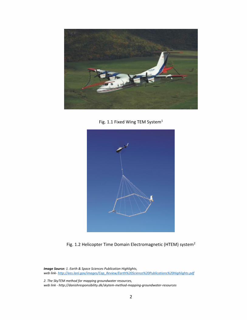
2
Fig. 1.1 Fixed Wing TEM System1
Fig. 1.2 Helicopter Time Domain Electromagnetic (HTEM) system2
Image Source: 1. Earth & Space Sciences Publication Highlights, web link- http://ees.lanl.gov/images/Cap_Review/Earth%20Science%20Publications%20Highlights.pdf
2. The SkyTEM method for mapping groundwater resources, web link - http://danishresponsibility.dk/skytem-method-mapping-groundwater-resources
3
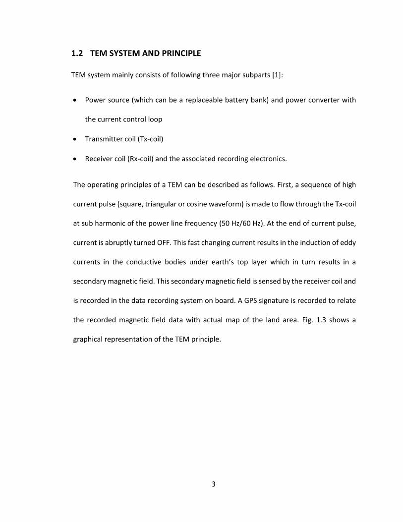
1.2 TEM SYSTEM AND PRINCIPLE
TEM system mainly consists of following three major subparts [1]:
Power source (which can be a replaceable battery bank) and power converter with
the current control loop
Transmitter coil (Tx-coil)
Receiver coil (Rx-coil) and the associated recording electronics.
The operating principles of a TEM can be described as follows. First, a sequence of high
current pulse (square, triangular or cosine waveform) is made to flow through the Tx-coil
at sub harmonic of the power line frequency (50 Hz/60 Hz). At the end of current pulse,
current is abruptly turned OFF. This fast changing current results in the induction of eddy
currents in the conductive bodies under earth’s top layer which in turn results in a
secondary magnetic field. This secondary magnetic field is sensed by the receiver coil and
is recorded in the data recording system on board. A GPS signature is recorded to relate
the recorded magnetic field data with actual map of the land area. Fig. 1.3 shows a
graphical representation of the TEM principle.

4
Fig. 1.3 TEM Principle [4]
Fig. 1.4 shows the ideal waveforms for Tx- coil current, voltage and secondary field
response as recorded by the receiver in TEM systems [5]. It can be seen that the current
through the transmitter coil goes from zero to the peak reference value by applying a high
DC voltage. This peak reference current is maintained near its reference value by applying
current control techniques. After predefined ON period, the current through the coil is
made to fall sharply to zero. This sudden fall induces eddy current in the mineral target
which in turn produces secondary magnetic field. The secondary field response, as sensed
by the receiver is recorded once the OFF period starts. The secondary field due to
conductive mineral is highest just after the coil current goes to zero and it decays
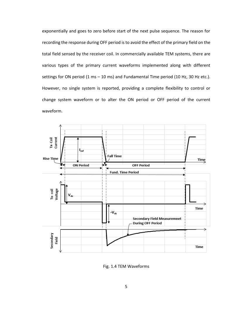
5
exponentially and goes to zero before start of the next pulse sequence. The reason for
recording the response during OFF period is to avoid the effect of the primary field on the
total field sensed by the receiver coil. In commercially available TEM systems, there are
various types of the primary current waveforms implemented along with different
settings for ON period (1 ms – 10 ms) and Fundamental Time period (10 Hz, 30 Hz etc.).
However, no single system is reported, providing a complete flexibility to control or
change system waveform or to alter the ON period or OFF period of the current
waveform.
Fig. 1.4 TEM Waveforms

6
1.3 THESIS OBJECTIVE AND CHALLENGES
This thesis deals with the following objectives
To design the power converter and control scheme to inject trapezoidal, unipolar
current pulses into transmitter coil of the TEM system.
Minimum current fall times (< 100 µs) for high reference current (200 A) shall be
achieved to generate better secondary response from mineral targets.
The converter control and data acquisition system shall be fast, providing a
sampling time in the range of 2 µs – 4 µs to provide better data resolution and
better current regulation.
The overall weight and size of the system are limited by the helicopter towing
capacity and hence the weight and size of the system shall be kept to minimum
(< 200 kg).
The power losses in the converter shall be minimized.
1.4 THESIS CONTRIBUTIONS
Design of a power converter and associated control to establish high current
trapezoidal pulses in the transmitter coil with current fall time less than 100 µs at
high current (200 A) with resultant di/dt of 2000 kA/s.
Maintaining a predefined constant current magnitude for the duration of
predefined pulse width using constant ON-Time control.
Implementation of LabVIEW based CompactRIO system to perform the data
acquisition and current control at a fast sampling rate (500 kHz).
7
Balancing the thermal stress in the IGBT switches by interchanging the gating
signals in alternate cycles.
Proposal of zero current switching technique to reduce the switching losses.
1.5 THESIS OUTLINE
The content of this thesis is organized into 5 Chapters.
Chapter 1 presents basic introduction to the AEM methods used in airborne survey
systems along with brief explanation of the TEM system components and working
principle.
Chapter 2 presents the review of the present power converter topologies used in airborne
electromagnetic survey systems along with the advantages and shortcomings of these
systems. A brief introduction is presented on the selection of the type of current
waveform for the transmitter coil.
Chapter 3 presents the simulation analysis of proposed converter topology with
hysteresis current control and constant ON-time control. Different modes of the
converter and the associated equations, governing the current waveform are discussed.
MATLAB simulation results are presented at low current and high current levels to
simulate the converter operation. Design procedure are presented to select DC link
capacitor, DC power source and RCD snubber components.
Chapter 4 presents the details about the implementation of the converter control scheme
by introducing various subsystems of NI CompactRIO architecture. LabVIEW programming
approach is presented for the proposed system in detail. Code optimization is discussed

8
to show the improvement steps followed during implementation stage to reduce the
sampling time. A problem of switch turn OFF delay is discussed along with the solution,
implemented using pull down resistors. The test results obtained from the system tests,
carried out at low power (125V, 60 A) and high power (500V, 200 A) are presented to
show the effectiveness of the designed system.
Chapter 5 presents the selection of the soft switching scheme to reduce the switching
power loss in the converter. The operation of soft switching converter topology is
discussed using state plane trajectory and design calculations are presented to select the
resonant elements considering the design criteria. MATLAB simulation results are
presented to verify the zero current switching design.
Chapter 6 summarizes the overall research conducted in this thesis and presents the final
conclusions. Suggestions for future work on this topic are presented.
9
CHAPTER 2. REVIEW OF POWER CONVERTER TOPOLOGIES IN
AEM SYSTEMS
2.1 INTRODUCTION
The AEM applications need a particular attention to the power converter design, to
control the excitation of current pulses in the transmitter coil (Tx-coil). Although AEM
systems are used for geophysical surveys for a long time and there is great amount of
work published and reported in the design optimization and configuration of transmitter
coil (Tx-coil) and receiver coil (Rx-coil) but there is very limited work published and
reported on the design of the power stage of these systems .However an attempt was
made to collect presently available literature pertaining to design of power converters for
TEM applications.
2.2 SELECTION OF CURRENT WAVEFORM
One of the starting point to design a TEM survey system is to select a current waveform
that results in the maximum response from the mineral target. Different type of current
waveforms (Triangular, Trapezoidal, Square, Cosine, Half – sine) are historically used in
airborne TEM methods. The previous work by [6] investigates the effect of different
transmitter coil waveforms on the system response recorded from the mineral deposit
and concludes that for the current pulses of same amplitude and width, the maximum
response is generated by a square current waveform. However due to the load time
constant, a perfect square waveform cannot be achieved in reality. Therefore in this work
the power stage is designed to provide a trapezoidal current pulse.
10
2.3 PRESENT CURRENT CONTROL TOPOLOGIES
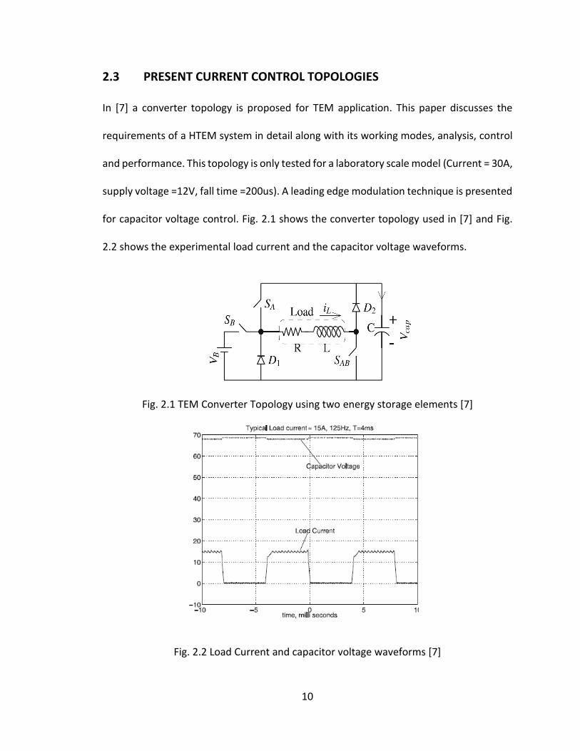
In [7] a converter topology is proposed for TEM application. This paper discusses the
requirements of a HTEM system in detail along with its working modes, analysis, control
and performance. This topology is only tested for a laboratory scale model (Current = 30A,
supply voltage =12V, fall time =200us). A leading edge modulation technique is presented
for capacitor voltage control. Fig. 2.1 shows the converter topology used in [7] and Fig.
2.2 shows the experimental load current and the capacitor voltage waveforms.
Fig. 2.1 TEM Converter Topology using two energy storage elements [7]
Fig. 2.2 Load Current and capacitor voltage waveforms [7]

11
Advantages:
1. Use of two energy storage elements reduces the current overshoot irrespective of
the sampling rate of the control system.
2. Good capacitor voltage regulation at different load current values (low current).
3. The topology presents low power loss due to recycling of the coil energy at the
end of pulse.
The information on the sampling rate of data acquisition and rate of the control system
is not presented.
Disadvantages:
1. The voltage of the capacitor is regulated to a reference value through energy
recovery from load to the capacitor during fall time. At high current levels the
capacitor voltage cannot be regulated at the reference value due to losses in the
circuit.
2. Absence of snubber circuits and implementation with hard switching technique
risks system safety.
3. The performance at high current levels is highly uncertain with this topology.
4. Data is not presented on the use of any special technique for data acquisition and
control and an important factor of sampling rate is not considered.
In [8], an inverter topology with clamped and unclamped circuit is presented for airborne
surveying systems. The main feature of the proposed topology is the fast reversal of the
12
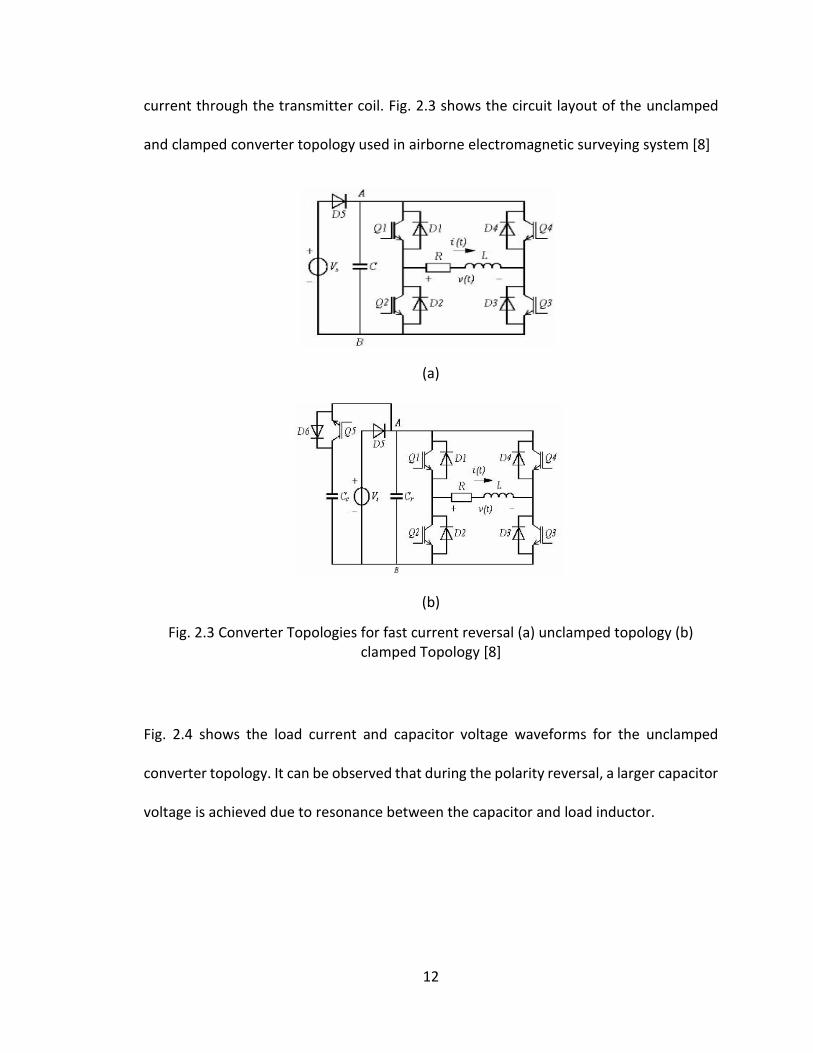
current through the transmitter coil. Fig. 2.3 shows the circuit layout of the unclamped
and clamped converter topology used in airborne electromagnetic surveying system [8]
(a)
(b)
Fig. 2.3 Converter Topologies for fast current reversal (a) unclamped topology (b) clamped Topology [8]
Fig. 2.4 shows the load current and capacitor voltage waveforms for the unclamped
converter topology. It can be observed that during the polarity reversal, a larger capacitor
voltage is achieved due to resonance between the capacitor and load inductor.
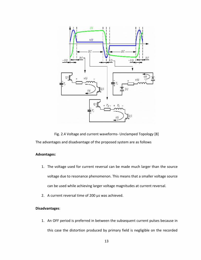
13
Fig. 2.4 Voltage and current waveforms- Unclamped Topology [8]
The advantages and disadvantage of the proposed system are as follows
Advantages:
1. The voltage used for current reversal can be made much larger than the source
voltage due to resonance phenomenon. This means that a smaller voltage source
can be used while achieving larger voltage magnitudes at current reversal.
2. A current reversal time of 200 µs was achieved.
Disadvantages:
1. An OFF period is preferred in between the subsequent current pulses because in
this case the distortion produced by primary field is negligible on the recorded

14
secondary field. However in the present work there is no provision for the OFF
period between the subsequent current pulses.
2. Clamped topology requires an additional capacitor and controlled switch that
adds to the cost, weight and additional losses in the system.
3. Bad switch utilization, no snubber protection, no soft switching mechanism
available.
2.4 CONCLUSION
Observing the work discussed in literature review it can be summarized that there is a
scope to design a new system that comprise a power source, converter topology,
transmission coil, receiver coil and data acquisition system that is efficient , utilizes less
number of system components, provides better control and performance. With the
improvement in semiconductor technology along with wider use of control and
acquisition tools such as LabVIEW, a new high power yet lighter and efficient system is
proposed. For implementation of the converter control scheme, a trapezoidal current
waveform is selected as the desired current waveform.

15
CHAPTER 3. THE PROPOSED POWER CONVERTER – DESIGN
AND SIMULATIONS
3.1 INTRODUCTION
This chapter presents the detailed design and simulation analysis of the power circuit and
the control scheme for controlling the current waveform in the transmitter coil. MATLAB
Simulink is used to simulate the performance of the proposed converter and associated
control before implementing the system. An attempt is made to provide the information
on important starting points defining the scope or the final output. The power converter
(Type – D chopper) topology modes are presented along with two current control
strategies. First, the current control is achieved by implementing widely used hysteresis
current control. However to limit the current overshoots caused by high di/dt and to
implement soft switching techniques later in the project work it is very important to have
a precise timing control over Turn - ON duration of the switch, which cannot be controlled
precisely by hysteresis current control. To achieve better switch timing control, a novel
constant ON-time control logic is developed and simulated in MATLAB Simulink and
successfully implemented during implementation phase. In the end of this chapter
concluding remarks are provided based on the simulation results.
3.2 IMPORTANT CONSIDERATIONS
The following points are considered at the start of the design procedure to define the
targeted performance from the system.

16
The transmitter coil is designed and optimized in different work. Already known
resistance value (55 mΩ) and inductance value (200 µH) are used for simulation
purposes.
Although a bipolar (positive and negative) current pulse waveform is a preferred
choice to cancel out the noise in the secondary field recorded by the receiver,
unipolar current sequences are considered in this work due to design simplicity
and cost effectiveness of the converter.
To avoid interference with the power line frequency, the fundamental time period
of the current waveform is selected as sub harmonic of the power line frequency
(50 Hz/60 Hz) [9]. To implement unipolar current waveforms in this work, the
fundamental time period is selected as 50 Hz/60 Hz. In next stage of development,
system will be modified to generate bipolar current pulses at 25 Hz/30 Hz
fundamental frequency.
Ideally a square current waveform, to achieve maximum secondary field response
from the mineral target would be used [10].However due to presence of high coil
inductance, a trapezoidal pulse waveform with sharp rise and fall times is a
practically feasible choice.
The time for which the current is maintained near the peak reference value is
referenced as pulse width and is fixed to 2 ms [11].
As the final system implementation is based on CompactRIO Platform from NI
hence the simulation time step and the controller time step (same as sampling
17
time) are selected considering the FPGA clock rate of 25 ns and analogue Input
module rate of 500 KS/s/channel respectively.
The final target for the fall time is fixed at 100 µs based on other available system
studies [13].
The ideal Simulink models are considered for the IGBTs, diodes and other passive
elements.
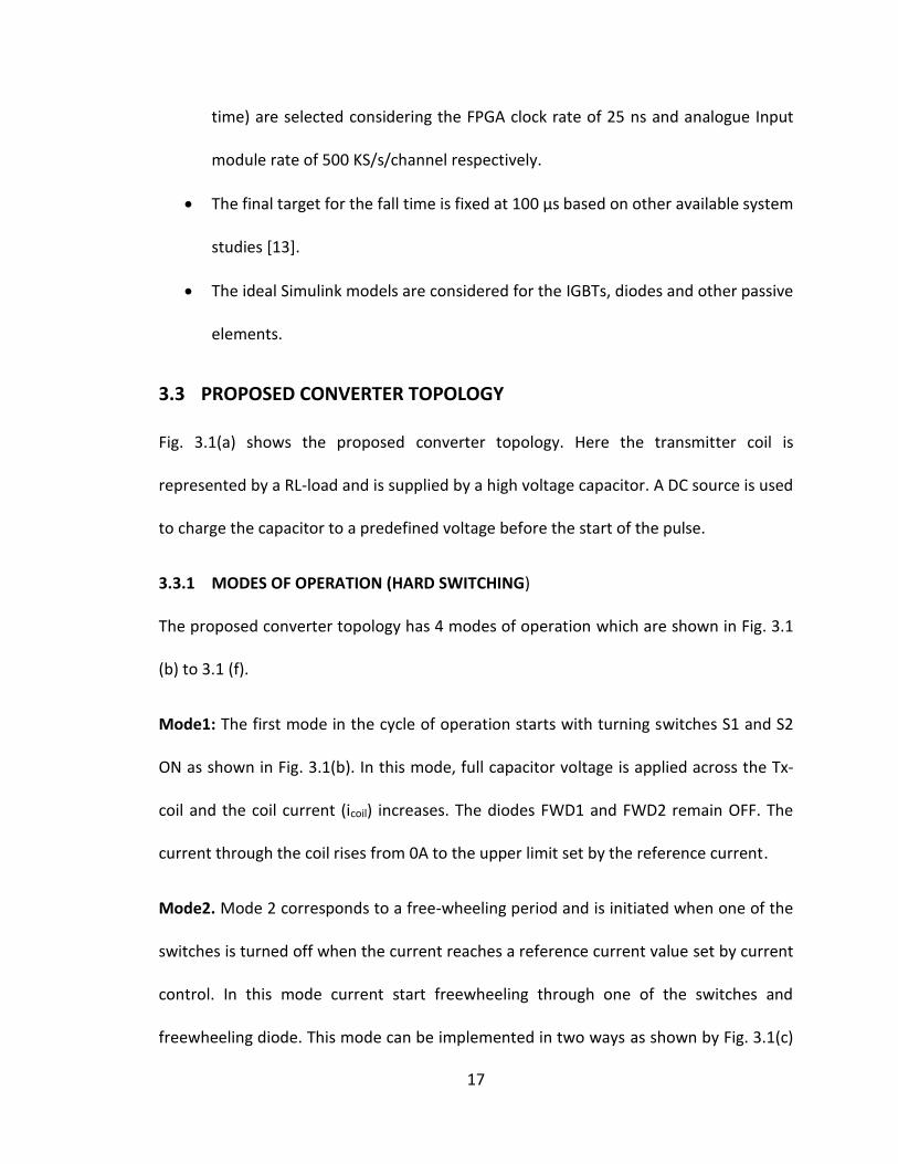
3.3 PROPOSED CONVERTER TOPOLOGY
Fig. 3.1(a) shows the proposed converter topology. Here the transmitter coil is
represented by a RL-load and is supplied by a high voltage capacitor. A DC source is used
to charge the capacitor to a predefined voltage before the start of the pulse.
3.3.1 MODES OF OPERATION (HARD SWITCHING)
The proposed converter topology has 4 modes of operation which are shown in Fig. 3.1
(b) to 3.1 (f).
Mode1: The first mode in the cycle of operation starts with turning switches S1 and S2
ON as shown in Fig. 3.1(b). In this mode, full capacitor voltage is applied across the Tx-
coil and the coil current (icoil) increases. The diodes FWD1 and FWD2 remain OFF. The
current through the coil rises from 0A to the upper limit set by the reference current.
Mode2. Mode 2 corresponds to a free-wheeling period and is initiated when one of the
switches is turned off when the current reaches a reference current value set by current
control. In this mode current start freewheeling through one of the switches and
freewheeling diode. This mode can be implemented in two ways as shown by Fig. 3.1(c)

18
and Fig. 3.1(d). In first case, switch S2 is kept ON and switch S1 is commutated to maintain
the current near the reference value for the required duration of pulse width. In second
case, switch S1 is kept ON and switch S2 is commutated to achieve current control. Case
1 and case 2 are applied in alternate pulse cycles to share the switching losses and thermal
stress among the two IGBTs.
Mode 3: Once the desired pulse width is reached, both the switches S1 and S2 are turned
OFF (Fig. 2(e)). Due to inductive nature of the circuit, diode FWD1 and FWD2 are turned
ON at this instant and a negative DC link voltage is applied across the coil. This results in
sharp decay in current from reference value to zero. During this mode, part of the energy
stored in the coil is fed back to the DC link capacitor. As the current reaches 0A, the diodes
are naturally commutated to OFF state and this marks the end of Mode 3.
Mode 4: In the next mode, Mode 4 , the coil remains isolated form the DC link capacitor
hence there is no transfer of energy from the capacitor to coil or vice versa. During this
mode the response from the mineral deposit is sensed by the receiver coil and is recorded
for post processing. Also at the end of Mode 3, due to energy losses in circuit elements
the capacitor voltage is not fully recovered back to the initial value. Hence the power
supply is enabled to bring the DC link capacitor voltage back to the reference value. The
circuit for this condition is shown in Fig. 3.1 (f). The end of fundamental time cycle marks
the end of Mode 4 and initiates next cycle of operation.
19
Vdc
Lcoil
S2
S1
FWD1
FWD2
RcoilCdcDC
SourceDC
Vdc
Lcoil
S2
S1
FWD1
FWD2
RcoilCdcDC
Source
DC
(a) Proposed Hard Switching Topology (b) Mode-1
Vdc
Lcoil
S2
S1
FWD1
FWD2
RcoilCdc
DC Source
DC
Vdc
Lcoil
S2
S1
FWD1
FWD2
RcoilCdc
DC Source
DC
(c) Mode-2(a) (d) Mode- 2(b)
Vdc
Lcoil
S2
S1
FWD1
FWD2
RcoilCdcDC
SourceDC
Vdc
Lcoil
S2
S1
FWD1
FWD2
RcoilCdcDC
SourceDC
(e) Mode- 3 (f) Mode- 4
Fig. 3.1 Proposed Topology & Modes of Operation (Hard Switching)
20
3.3.2 CURRENT GOVERNING EQUATIONS
Before starting the simulation of the proposed converter topology, it is important to
model the governing equations and then design and select the system components based
on the system requirements. First of all as shown in Mode-1 (Fig. 3.1 (b)), the switches S1
and S2 are closed and the circuit becomes a series RLC resonant circuit. The equations
governing the series RLC resonance circuit defines the current flow through the load (Tx-
coil). The series RLC resonance circuit can be designed to act as over damped, critically
damped or underdamped state by selecting the value of circuit elements. However for a
given capacitor voltage, the system developed for underdamped conditions will result in
least current rise and fall times.
The current through the circuit in Mode-1 can be represented by following exponential
rise equation [14] [15]
𝑖𝑐𝑜𝑖𝑙 =𝑉𝑑𝑐
𝜔𝐿𝑐𝑜𝑖𝑙𝑒−𝜎𝑡 𝑠𝑖𝑛(𝜔𝑡) (3.1)
Where
𝜔 = √ 1
𝐿𝑐𝑜𝑖𝑙𝐶𝑑𝑐− (
𝑅𝑐𝑜𝑖𝑙
2𝐿𝑐𝑜𝑖𝑙)
2
(3.2)
𝜎 =𝑅𝑐𝑜𝑖𝑙
2𝐿𝑐𝑜𝑖𝑙 (3.3)
icoil = Instantaneous current through Tx- coil
Vdc = DC link capacitor voltage
Lcoil= Tx-coil inductance = 200 µH
Rcoil = Tx-coil resistance = 55 mΩ

21
Cdc = DC link capacitor rating
During Mode-2, the coil current freewheels and the zero voltage is applied across the coil,
the stored energy is dissipated mainly in the coil resistance. However the resistance of
the IGBT switches and the diodes also contribute to some energy loss but for this equation
modeling, the small contribution of these factors is not comparable and hence neglected.
The current in the Tx-coil during Mode2 is given by following equation [16]
𝑖𝑐𝑜𝑖𝑙 = 𝐼𝑥1 𝑒−𝜎′𝑡 (3.4)
Where Ix1= Tx- coil current at the beginning of Mode 2
And
𝜎′ =𝑅𝑐𝑜𝑖𝑙
𝐿𝑐𝑜𝑖𝑙 (3.5)
Similarly, in Mode-3, when both the switches are turned OFF and the diodes FWD1 and
FWD2 conducts , the stored energy of the coil is fed back to the DC link capacitor and coil
current decays from its peak value to zero.
The current in this phase is governed by following equation [16]
𝑖𝑐𝑜𝑖𝑙 = 𝐼𝑥2𝑒−𝜎𝑡 ((cos (ωt) −𝜎
𝜔sin(𝜔𝑡)) (3.6)
Where Ix2 = Tx-coil current at the beginning of Mode 3.
During Mode 4, the coil remains isolated from the power source and the DC link capacitor.
Hence no current flows through the Tx-coil for this period until the two switches are
turned ON at the start of next current cycle.

22
3.3.3 SELECTION OF DC LINK CAPACITOR
The Tx- coil fabricated for this work is a circular coil (stranded copper cable) with 4 turns
and diameter of 5m (Area = 19.6 m2). The dipole moment is fixed to 15000 N-m2 after
studying the present TEM systems [2]
So the required current can be calculated as
Dipole moment, M= N * Iref * A (3.7)
Where N = No. of turns of Tx-coil
Iref = Reference Tx- coil current
A = Area of Tx- coil
By using equation 3.7, the peak DC current is fixed at 200 A.
For driving this current to the coil, the DC link capacitor voltage is fixed to 500 V.
From equation (3.2), ω can be represented in terms of Cdc.
From equation (3.5) σ = 137.5 Nepers/s
Putting t= 100 µs, Ix2= 200 A, Icoil = 0 and solving for Cdc, the required value of Cdc is
calculated and the closest standard capacitor rating selected is 1000 µF.
The capacitor voltage rating is selected considering the future implementations with
higher current ratings.
The final capacitor ratings selected is, voltage rating =1500 VDC, Capacitance =1000 µF.

23
3.3.4 SELECTION OF DC POWER SOURCE
The next step is to select the DC power source that can efficiently charge the capacitor in
available time, in-between the current pulses. One of the important point is to select a
DC power supply with the provision of remote control i.e. to have a flexibility to control
the output voltage of the DC power supply through a user interface. The other important
factors to be considered are the output voltage rating and the output current. For this
purpose, high power capacitor charging power supplies from TDK Lambda Americas Inc.
are found suitable. The equations given in application note [17] are used to select the
power source rating for a given charging time of the capacitor.
As per the application note [17], the peak power required from the power source is given
by the following equation
𝑃𝑝𝑒𝑎𝑘 =0.5∗𝐶𝑑𝑐∗𝑉𝑝𝑠∗𝑉𝑑𝑐
𝑇𝑐 (3.8)
Where Cdc = DC link capacitor rating
Vps = Output voltage rating of power source
Vdc = DC link Capacitor voltage
Tc = Capacitor Charging Time
As pulse width and fundamental time period for the current pulse is fixed to 2ms and
16.67ms respectively. Therefore the capacitor charging time cannot be more than
16.67ms, if the power supply is always kept connected to the DC capacitor. However it’s
preferred to connect the power supply only during current OFF period as the power

24
supply can provide limited amount of current and if it is kept connected to the load all the
time the overload protection may cause inhibit action. Effectively maximum value for Tc
can be considered equal to 14 ms. Here, Vdc is the difference in the voltage that power
supply has to provide in between the current pulses. From the simulation results of next
section it can be seen that the drop in the voltage for 500V, 200A operation is around 15V
but a part of it is recovered by the energy recovery from the coil. Hence to calculate the
power rating of the power supply, Vdc can be considered around 12V. Using the earlier
calculated capacitance of DC link capacitor along with Vdc=12 V, and Tc = 14 ms, in
equation (3.8), a value of peak power was calculated for the power source. The power
supply finalized was 1KW, 3KV (102-3kV-POS-5V-LP) from TDK Lambda. A 15 pin D-type
female connector located on the power source provides the access to connect the remote
interface cable from manual control interface to the power source.
3.3.5 SELECTION OF IGBTS
As in all converter applications to select the IGBT switches, the important aspect is to
calculate or fix the current and voltage specifications as per the application needs.
However in this application additional constraints are put by weight and size of the power
converter and hence attention is given to choose the modular, light yet powerful switch
modules. Although there are various IGBT product families available from manufacturers
such as Infineon, Powerex and On Semiconductors, but for this application, Semix IGBT
modules from Semikron are selected due to their modular and compact design, Cost
effectiveness and superior performance at high power levels.
The other advantages of Semix modules are [18]

25
Single housing contains the IGBT and free-wheeling diode, and needs only one switch
assembly for each converter leg resulting in compact size and lower cost of the
converter.
The modular design of Semix IGBT modules result in low – inductance design as the
DC link connections can be short, resulting in reduced voltage overshoot.
Due to directly mounted driver board optimum gate drive performance can be
achieved (with minimum noise)
The reduced solder joints or the connections result in better system reliability.
Considering the future scope of testing at higher power levels, 1200V, 600A IGBT modules
are selected. These modules can handle switching frequencies up to 10 KHz with 100%
duty cycle. More details on implementation of these IGBT modules is provided in Chapter
4.
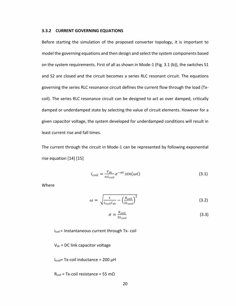
3.3.6 SIMULATION RESULTS
The simulation analysis was conducted using MATLAB Simulink. Table 3-1 shows the
major parameter values considered for the simulation with hysteresis current control
26
Table 3-1 Simulation Parameters
Parameter Symbol Value Units
Reference Tx- coil current Iref 200 A
Initial DC link capacitor voltage Vdc 500 V
DC Link capacitor rating Cdc 1000 µF
DC power source peak charging rate Ppeak 1100 J/s
DC power source output voltage rating Vrated 3 KV
Tx-coil inductance Lcoil 200 µH
Bus bar stray inductance Lstray 200 nH
Current pulse width T1 2 ms
Fundamental time period T2 16.67 ms
Simulation time step Tsim 25 ns
Controller sampling time Tctr 2 µs
Hysteresis band Iband ±5 A
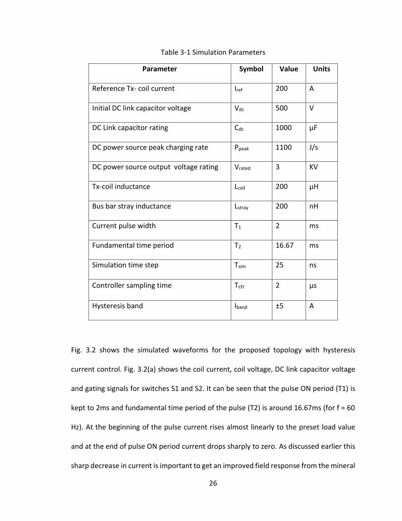
Fig. 3.2 shows the simulated waveforms for the proposed topology with hysteresis
current control. Fig. 3.2(a) shows the coil current, coil voltage, DC link capacitor voltage
and gating signals for switches S1 and S2. It can be seen that the pulse ON period (T1) is
kept to 2ms and fundamental time period of the pulse (T2) is around 16.67ms (for f = 60
Hz). At the beginning of the pulse current rises almost linearly to the preset load value
and at the end of pulse ON period current drops sharply to zero. As discussed earlier this
sharp decrease in current is important to get an improved field response from the mineral
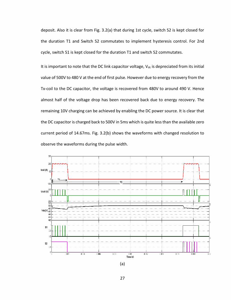
27
deposit. Also it is clear from Fig. 3.2(a) that during 1st cycle, switch S2 is kept closed for
the duration T1 and Switch S2 commutates to implement hysteresis control. For 2nd
cycle, switch S1 is kept closed for the duration T1 and switch S2 commutates.
It is important to note that the DC link capacitor voltage, Vdc is depreciated from its initial
value of 500V to 480 V at the end of first pulse. However due to energy recovery from the
Tx-coil to the DC capacitor, the voltage is recovered from 480V to around 490 V. Hence
almost half of the voltage drop has been recovered back due to energy recovery. The
remaining 10V charging can be achieved by enabling the DC power source. It is clear that
the DC capacitor is charged back to 500V in 5ms which is quite less than the available zero
current period of 14.67ms. Fig. 3.2(b) shows the waveforms with changed resolution to
observe the waveforms during the pulse width.
(a)
28
(b)
Fig. 3.2 Simulation waveforms with hysteresis current control
(a) Two pulse cycles (b) One pulse cycle (Simulation parameters shown in Table-3-1)
3.4 CONSTANT ON - TIME CURRENT CONTROL SCHEME
As discussed in earlier sections one of the important requirements of the TEM system is
to inject a trapezoidal current pulse through the Tx-coil. The current can be maintained
near the reference value by applying widely used digital hysteresis current control. A
digital hysteresis current control was implemented using standard Relay function of
LabVIEW and alternatively by using S-R flip-flop logic. However in each case the minimum
achievable sampling time was 6 μs. This leads to current overshoot beyond the values set
by control input (a common problem associated with hysteresis current control) [19]. Also
high sampling times will result in low data resolution of the secondary field survey data

29
as same system is to be used for recording the secondary field response. The high
sampling time is contributed to the more processing power utilized by the control code
implementation using flip-flops and Relay function. This condition is also not favorable to
design a soft switching scheme for the converter, as the ON- time or OFF time cannot be
controlled effectively by employing hysteresis current control.
To avoid these problems, a time based control strategy is needed where the switch is
allowed to stay ON for a predefined time interval. To achieve this, a novel control strategy
referred as Constant ON time control was conceptualized and implemented.
The main attributes of this new technique are
Results in a better control where the ON- Time for the IGBT switch is directly
controlled by passing a numerical control on the host screen.
Constant ON- Time logic can be implemented in the LabVIEW using case structure
architecture which uses less processing power of the controller and is fast to
execute as compared to sequential logic control (Hysteresis control using relay VI
or SR flip Flops).
A MATLAB Simulink standard function block was used to write a function to perform this
control logic. Fig. 3.3 shows the flow chart explaining the logic of constant ON-time
current control scheme.
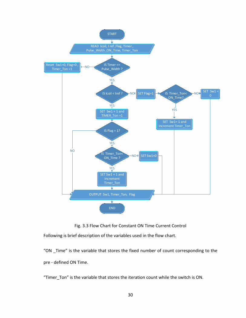
30
START
IS Timer <= Pulse_Width ?
YES
IS Icoil < Iref ?
READ Icoil, I ref ,Flag, Timer , Pulse_Width ,ON_Time, Timer_Ton
YES
SET Sw1 = 1 and TIMER_Ton =1
IS Flag = 1?
SET Sw1 = 1 and Increment Timer_Ton
NO SET Flag=1 IS Timer_Ton< ON_Time?
YES
SET Sw1= 1 and Increment Timer_Ton
SET Sw1 = 0
NOReset Sw1=0, Flag=0 ,
Timer_Ton =1
YES
IS Timer_Ton< ON_Time ?
YES
NO SET Sw1=0
OUTPUT Sw1, Timer_Ton, Flag
END
NO
NO
Fig. 3.3 Flow Chart for Constant ON Time Current Control
Following is brief description of the variables used in the flow chart.
“ON _Time” is the variable that stores the fixed number of count corresponding to the
pre - defined ON Time.
“Timer_Ton” is the variable that stores the iteration count while the switch is ON.

31
“Timer” is the counter that counts the number of iterations for the fundamental time
period.
“Pulse_Width” represents the fixed time for which the square current waveform is
present.
“Flag” is used as a memory element to store the information when the coil current
exceeds the reference current first time. It is activated whenever the coil current crosses
the value of reference peak current first time. Variable “Flag” is reset when the end of the
desired current pulse is reached.
The operation of the TEM with the constant ON-time current control scheme was
simulated in MATLAB Simulink. At the start, the parameters such as coil current,
reference peak current, pulse width, flag status and timer values are read from the
MATLAB workspace and are passed to the function block containing the constant ON-
Time program logic. In the initial phase, when the coil current is less than the reference
current, the switch stays ON.
After the initial rise of the current, whenever coil current crosses the reference peak
current, “Timer _Ton” is incremented and is compared with “ON_Time” for each loop
iteration. Switch S1 remains ON until “Timer_Ton” is less than “ON_Time”, resulting in
current rise and “Timer_Ton” keep on updating. Switch S1 is turned-OFF when
“Timer_Ton” becomes equal to “ON_Time”, resulting in freewheeling of coil current
through freewheeling diode and Switch S2. The coil current is decayed slowly and when
it reaches a value less than reference peak current the “Timer_Ton” is reset, Switch S1 is

32
turned - ON again and value of “Timer_Ton” is incremented in subsequent Iterations for
the defined duration of “ON_Time”.
To balance the thermal stress of the IGBT modules, the alternate switch operation (used
with hysteresis current control) is retained in constant ON – Time control technique.
Fig. 3.4 (a) shows the overall waveforms for one pulse width period. The coil current and
DC capacitor voltage waveforms are similar to the one achieved with hysteresis current
control. From Fig. 3.4 (b), it can be observed that as soon as the coil current falls below
the reference current, the value of “Timer_Ton” start increasing and Switch S1 is turned
ON resulting in increase in coil current. After a time of 4 µs the value of “Timer_Ton”
becomes equal to 160 (i.e. 4 µs/ 25 ns) and the switch S1 is turned-OFF, and “Timer_Ton”
keeps its value until the coil current falls below reference current. The converter was
simulated with different values of ON_Time and corresponding effect was observed in the
simulation results.
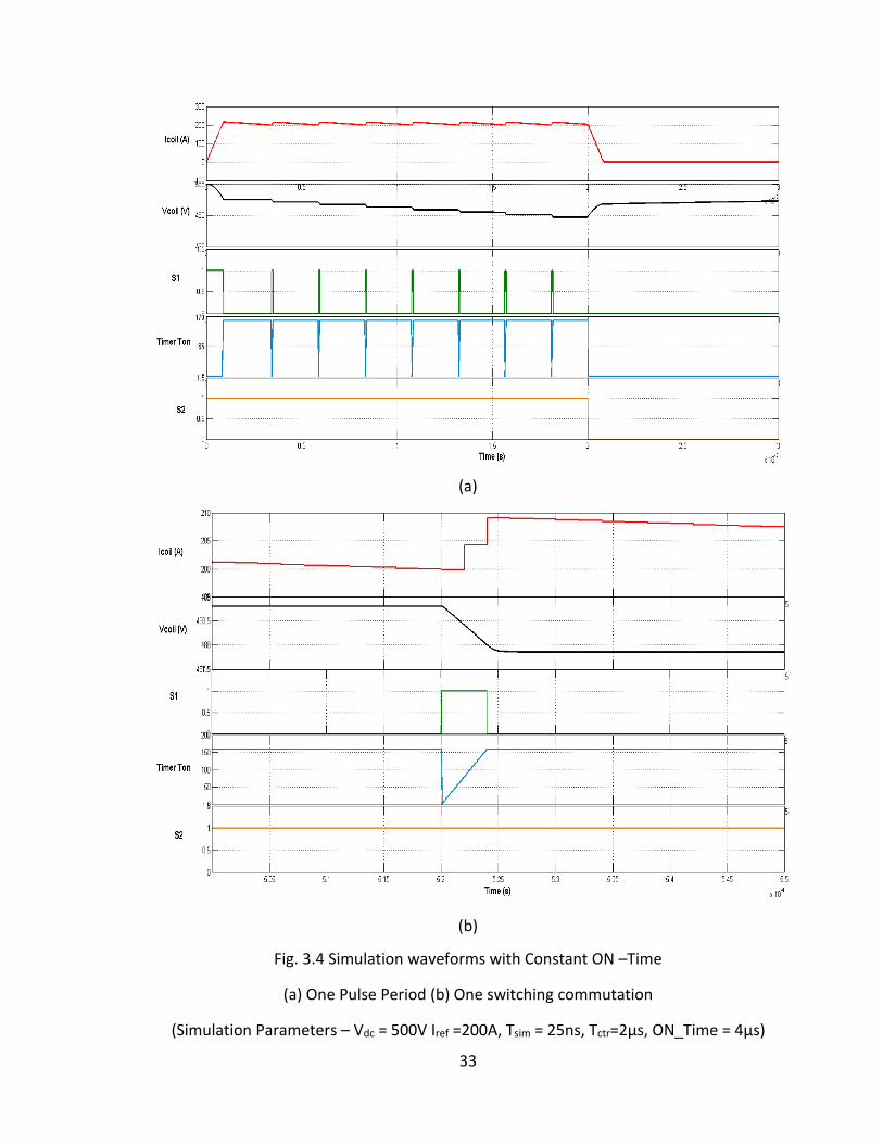
33
(a)
(b)
Fig. 3.4 Simulation waveforms with Constant ON –Time
(a) One Pulse Period (b) One switching commutation
(Simulation Parameters – Vdc = 500V Iref =200A, Tsim = 25ns, Tctr=2µs, ON_Time = 4µs)
34
3.5 DESIGN OF SNUBBER CIRCUIT
During the discussion of operating modes of the converter in section 3.3.1 the stray
inductance due to DC bus was neglected. However in practice, there is always a DC loop
stray inductance associated with the DC bus and whenever the IGBT switch is turned OFF,
the trapped energy in the stray inductance results in voltage overshoot. In high power
applications similar to the case under consideration, this voltage overshoot can reach to
a magnitude that can possibly damage the switch and other circuitry. One of the ways to
keep the stray inductance to minimum is to keep the DC link conductor lengths to
minimum and to carefully design the DC link conductors with minimum overlap lengths.
But these design considerations can’t completely eliminate the stray inductance and
hence a solution is required to suppress the voltage overshoot at the IGBT terminals. To
protect the circuit elements from switching transients the solution proposed in literature
[20] [21] is to use a snubber circuit.
3.5.1 ADVANTAGES OF RCD SNUBBER
There are various type of snubber circuits that can be used in different applications and
their advantages and disadvantages are discussed in detail in [20]. For this application,
RCD snubber is used due to following advantages:
1. Suitable for medium and high power applications
2. Suitable for high frequency operation.
3. Can be implemented by using direct mount snubber modules with minimum
circuit length and hence minimum parasitic and stray inductance.
35
4. The snubber diode prevents any oscillations between snubber capacitor and DC
capacitor. These oscillations are otherwise present in the case of Decoupling
Capacitor.[21]
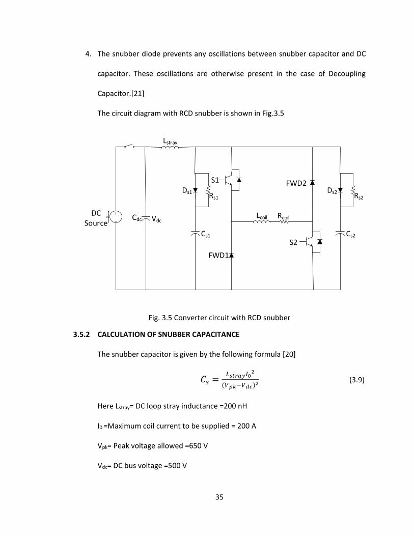
The circuit diagram with RCD snubber is shown in Fig.3.5
VdcLcoil
S2
S1
FWD1
FWD2
RcoilCdc
Ds1 Rs1
Cs1
Lstray
DC
Ds2
Cs2
Rs2
DC Source
Fig. 3.5 Converter circuit with RCD snubber
3.5.2 CALCULATION OF SNUBBER CAPACITANCE
The snubber capacitor is given by the following formula [20]
𝐶𝑠 =𝐿𝑠𝑡𝑟𝑎𝑦𝐼0
2
(𝑉𝑝𝑘−𝑉𝑑𝑐)2 (3.9)
Here Lstray= DC loop stray inductance =200 nH
I0 =Maximum coil current to be supplied = 200 A
Vpk= Peak voltage allowed =650 V
Vdc= DC bus voltage =500 V

36
Putting these values in equation (3.9)
Cs = 0.35µF
A near standard capacitor rating available is 0.47 µF and the voltage rating of the
capacitor selected is 1200 V
3.5.3 CALCULATION OF SNUBBER RESISTOR
The snubber resistor can be calculated by formula [21]
𝑅𝑠 = 1
6 𝐶𝑠𝑓𝑠𝑤 (3.10)
Where Cs = snubber capacitor (calculated above)
fsw= switching frequency of Switch S1
Here the switch S1 is commutating for a period of 2 ms and then remains in OFF state till
the end of fundamental time period. For a pulse ON period of 2ms and fundamental time
period of 16.67ms the switch S1 behavior during switching is observed in the MATLAB
simulation. It is seen that for a load current of 200A , DC capacitor voltage 500V and ON-
Time of 4 µs, the switching period of switch S1 is 200 µs giving a switching frequency, fsw=
5000 Hz. Using this value in equation (3.10) snubber resistor value of 71 ohm is calculated.
Power rating of the snubber resistor is given by
𝑃𝑅𝑠 = 0.5𝐶𝑠(𝑉𝑝𝑘2 − 𝑉𝑑𝑐
2)𝑓′𝑠𝑤 (3.11)
Here the effective frequency f’𝑠𝑤 = f𝑠𝑤 ∗𝑇1
𝑇2 (3.12)
Where T1 = Pulse ON Time = 2ms

37
And T2 = Fundamental Time Period = 16.67ms
Hence from equation (3.12), f’sw = 588 Hz
Substituting these values in equation (3.11) yield
PRs = 61 W
A standard resistor with ratings 75ohm, 100W (non- inductive design) with product no.
“MP9100-75.0F-ND” from Caddock Electronics Inc. was selected.
While implementing the snubber design, it is always advantageous to keep the parasitic
inductance of the snubber circuit layout to minimum. With individual element R, C and
diode there will be unavoidable inductance associated with the circuit layout. To
effectively implement the snubber design, the direct mount IGBT capacitor module
“SCM474K122H8N24-F” from Cornell Dubillier was used .The direct mounting results in
minimum parasitic inductance resulting in a better snubber implementation. It is a direct
mount module containing snubber capacitor and snubber diode in a single housing and
having an external connection to install the snubber resistor. The module’s DC voltage
rating is 1200V.
3.6 CONCLUSION
In this chapter, based on predefined scope the operating modes are discussed for the
class -D converter along with the equations defining the current waveform during these
modes. A detailed design approach is described to select the system components.
MATLAB Simulink analysis is presented to evaluate the performance of the power

38
converter. A constant ON –time control technique is explained to achieve better timing
control. In the end, to protect the IGBT and the converter circuitry from switching voltage
overshoots, a RCD snubber design is presented. The verification of the snubber design
cannot be performed in MATLAB simulation due to ideal component behavior. However
the effect of snubber circuit is evaluated in experimental tests presented in Chapter 4.

39
CHAPTER 4. HARDWARE IMPLEMENTATION AND
EXPERIMENTAL RESULTS
4.1 INTRODUCTION
This chapter presents the implementation of the proposed converter scheme along with
the associated digital control and data acquisition hardware. The LabVIEW programming
logic implemented to control the current waveform is presented in detail. The experiment
results are presented to display the performance of the entire system at different
development stages. An attempt is made to describe the process of LabVIEW code
optimization to achieve least possible sampling rates as per the installed hardware
capabilities. A problem of switch turn OFF delay was observed and a solution was
implemented using pull down resistances. In the end the conclusions are stated.
NOTE: The experimental setup was developed and tested at Laval facility of Geo Data
Solutions GDS Inc. Canada.
4.2 INTRODUCTION TO LABVIEW
LabVIEW (Laboratory Virtual Instrumentation Engineering Workbench) is a graphical
programming environment that, with help from logic blocks and other components,
makes it possible to test, simulate and control flowchart-type model [23]. It is easily
integrated with hardware devices such as the FPGA. Mostly the block diagram (where the
logic circuit is drawn) and the front panel (the input/output data and the programmatic
interface) is used when dealing with this program. Except the fact that a graphical

40
programming language is more user-friendly, the LabVIEW software has benefits
considering the following two big differences from other programming languages:
Graphical programming is realized with help from graphical icons, combined in a
diagram and is then directly compiled to machine code, so that the processor can
understand and execute the orders created in the diagram.
Data flow is transmitted in form of data (not lines of text). This makes it easier to
control different executions done separately and consecutively
4.3 INTRODUCTION TO FPGA
Field-programmable gate arrays (FPGAs) are reprogrammable silicon chips. In contrast to
processors in a PC, programming an FPGA rewires the chip itself to implement the
functionality rather than run a software application.
Benefits of Using FPGAs:
Faster I/O response times and specialized functionality
Exceeding the computing power of digital signal processors
Implementing custom functionality with the reliability of dedicated deterministic
hardware
Rapid prototyping and verification without the fabrication process of custom ASIC design
Field-upgradable eliminating the expense of custom ASIC re-design and maintenance
4.4 COMPACTRIO SYSTEM ARCHITECTURE
To implement the digital control of the proposed converter and to acquire the current
and voltage signals, National Instrument’s CompctRIO platform was selected.

41
CompactRIO is a reconfigurable embedded control and acquisition system and is vastly
used in modern control applications. The CompactRIO system’s hardware architecture
includes I/O modules, a reconfigurable FPGA chassis, and an embedded real time
controller [24]. CompactRIO is programmed with NI LabVIEW graphical programming
tools also known as G- Programming.
Due to faster control and data acquisition possible with embedded controller and the
modular design approach and the option to expand the cRIO architecture at any time by
adding additional input output modules with the same platform, CompactRIO was
selected to perform the control and acquisition tasks for this application.
The standard CompactRIO system selected for this application consists of following sub
parts [24]:
4.4.1 REAL TIME CONTROLLER (NI CRIO 9014):
It’s an embedded controller that runs the application code in the FPGA target and
interfaces FPGA target with C series I/O modules. It has 400 MHz processor, 2GB non
volatile storage and 128 MB DRAM. It supports RS 232 serial port for connection to the
peripherals. Alternatively an Ethernet port is used in this application for communication
between the real time controller and the host Computer. Also a USB slot can be used to
attach an external memory.

42
Fig. 4.1 NI cRIO-9014 RT controller
4.4.2 RECONFIGURABLE FPGA CHASSIS (NI CRIO 9111 -4 SLOT)
A four slot reconfigurable chassis is used to provide rugged modular housing to the Real
time controller and the C –series I/O modules. A backplane in the chassis contains the
FPGA target, and system’s data, timing and triggering buses. The FPGA chassis with
internal clock frequency of 40MHz is used in this application. In other words, FPGA
internal clock runs at a time step of 25ns that correspond to the FPGA tick rate and is used
as a unit to check the execution speed of the FPGA code. The application code is written
on the host computer and is compiled and downloaded to the reconfigurable FPGA target.
Xilinx Virtex-5 LX30 is the type of FPGA used in this chassis. The chassis comes with Din-
Rail Mounting or Panel Mounting options. In this application Din-Rail Mounting is selected
due to ease of mounting.

43
Fig. 4.2 NI cRIO-9111 four –slot, reconfigurable embedded chassis
4.4.3 ANALOG INPUT MODULE (NI 9222)
To acquire the Tx- coil current and DC capacitor voltage signals, a C- series 4- channel,
16 bit simultaneous analogue input module is selected. It has a sampling rate of 500
KS/s/ch which translates to a sampling time of 2us per channel. The input voltage range
for this module is ± 10V and comes with screw terminal connectivity.
Fig. 4.3 NI-9222 Analogue Input Module (4- Channel)
4.4.4 DIGITAL OUTPUT MODULE (NI 9474)
After acquiring the data from input channels the program code is executed in the FPGA
target and the output signals are generated for the IGBT switches and the Power Supply
Control. A C series, 8 channel, 1 us high speed digital output module is used for this
purpose. It has an output voltage range of 5 -30V.

44
Fig. 4.4 NI-9474 Digital Output Module (8- Channel)
4.4.5 CONTROLLER POWER SUPPLY (NI PS –15 POWER SUPPLY)
The function of this power supply is to power the CompactRIO controller and associated
hardware devices. The nominal input of this power supply is 115/230V AC and the output
is regulated 24VDC at 5A.
Fig. 4.5 NI PS-15 Power Supply
Fig. 4.6 shows the example of CompactRIO system assembly
45
Fig. 4.6 CompactRIO System
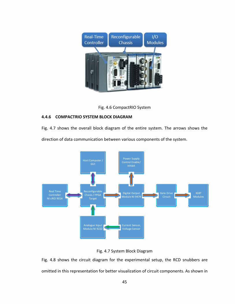
4.4.6 COMPACTRIO SYSTEM BLOCK DIAGRAM
Fig. 4.7 shows the overall block diagram of the entire system. The arrows shows the
direction of data communication between various components of the system.
Real Time Controller
NI cRIO 9014
Reconfigurable Chasis / FPGA
Target
Digital Output Module NI 9474
Host Computer / GUI
Current Sensor, Voltage Sensor
Gate Drive Circuit
IGBT Modules
Power Supply Control Enable/
Inhibit
Analogue Input Module NI 9222
Fig. 4.7 System Block Diagram
Fig. 4.8 shows the circuit diagram for the experimental setup, the RCD snubbers are
omitted in this representation for better visualization of circuit components. As shown in

46
Fig. 4.8, NI 9222 input module is connected to two sensors i.e. current sensor sensing the
Tx-coil current and voltage sensor sensing the DC capacitor voltage the same module can
be used to connect the input from the Rx-coil sensing the EM response from the target.
This input data is passed to the cRIO 9014 digital controller which is connected to the host
computer for two way data communication. CRIO9014 executes the control logic in the
FPGA target on reconfigurable chassis (FPGA code compiled in the host computer and
downloaded to the FPGA memory).Based on the real time input and the control logic, the
output control signals are sent to NI 9474 digital output module. There are three output
channels used, two to provide the gating pulses to the IGBTs gate drive circuits based on
the current control logic and one to enable or inhibit the DC Power Source based on the
capacitor voltage level.
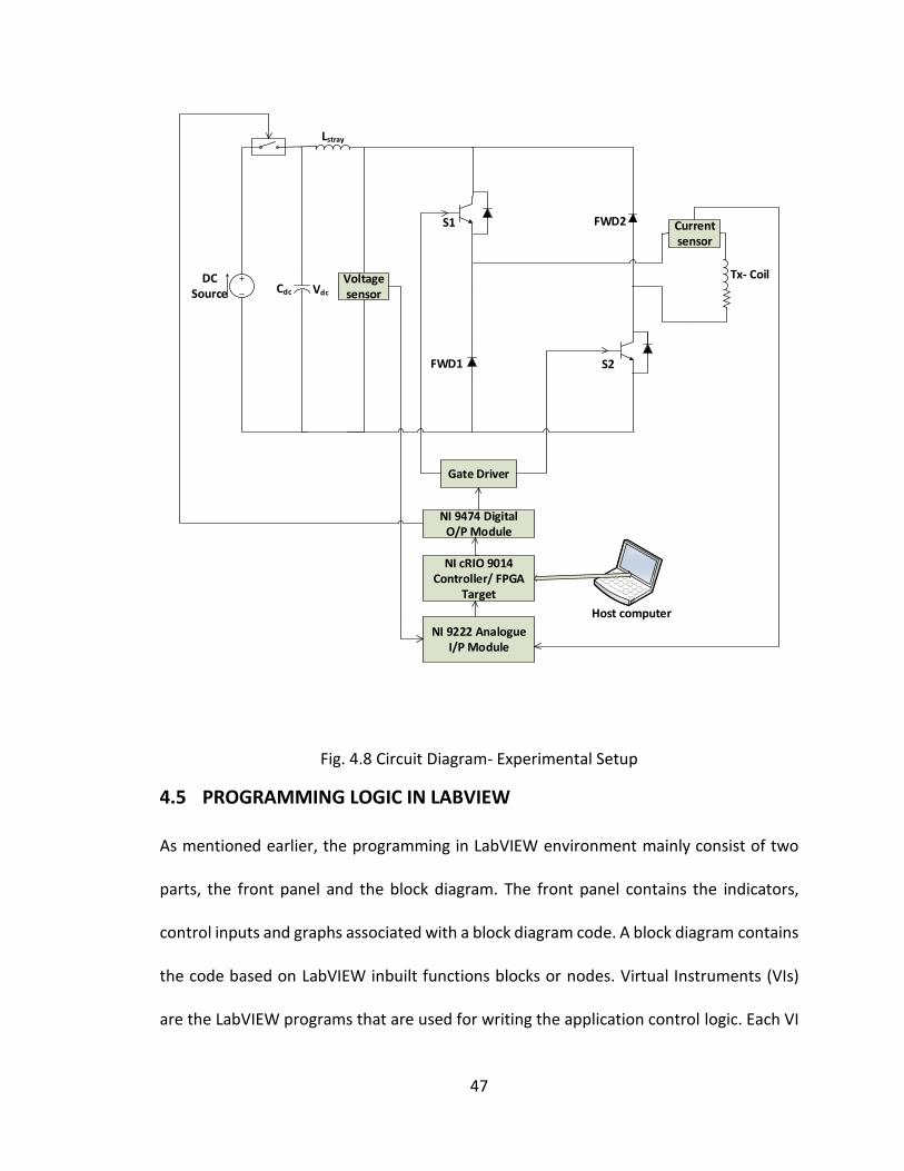
47
Vdc
Tx- Coil
S2
S1
FWD1
FWD2
Cdc
DC Source
Current sensor
Voltage sensor
Gate Driver
NI 9474 Digital O/P Module
NI cRIO 9014 Controller/ FPGA
Target
NI 9222 Analogue I/P Module
Host computer
Lstray
Fig. 4.8 Circuit Diagram- Experimental Setup
4.5 PROGRAMMING LOGIC IN LABVIEW
As mentioned earlier, the programming in LabVIEW environment mainly consist of two
parts, the front panel and the block diagram. The front panel contains the indicators,
control inputs and graphs associated with a block diagram code. A block diagram contains
the code based on LabVIEW inbuilt functions blocks or nodes. Virtual Instruments (VIs)
are the LabVIEW programs that are used for writing the application control logic. Each VI

48
has three main subparts – the front panel window, the block diagram and the icon/
connector pane. The front panel window acts as the user interface for the VI. The front
panel window may contains controls and indicators that interact with the VI to pass or
receive the data. Block Diagram window is used to write the application code using
graphical representation of functions to control the front panel objects. The block
diagram window contains the graphical source code for an application. Front panel
objects appear as terminals on the block diagram. The connector pane allows to use and
view a VI in another VI as a sub –VI.
The LabVIEW program code for this application contains 2 main virtual instruments (VIs)
1. GUI.vi 2.FPGA.vi
4.5.1 GUI.VI
In this work, a separate GUI as shown in Figure 4.9, is created on the host computer to
pass the user defined control parameters to the FPGA code (hysteresis current control).
GUI shown in Fig. 4.10 is used for the application using constant ON-Time control. The
parameters controlled through GUI are reference current, DC bus voltage, ON-time (Band
timer), Pulse Width, Sampling Rate and No of channels read by DMA FIFO. Graphical user
interface, GUI is also used to display the DC bus voltage, FPGA loop tick rate and actual
sampling rate achieved during run time. Three buttons are created with individual
function to start the firing of the converter switches , reset the power supply in case the
Power Supply goes into inhibit state and to give a stop command to the data acquisition
loop . A data file path selection window is provided to select the path where a data file
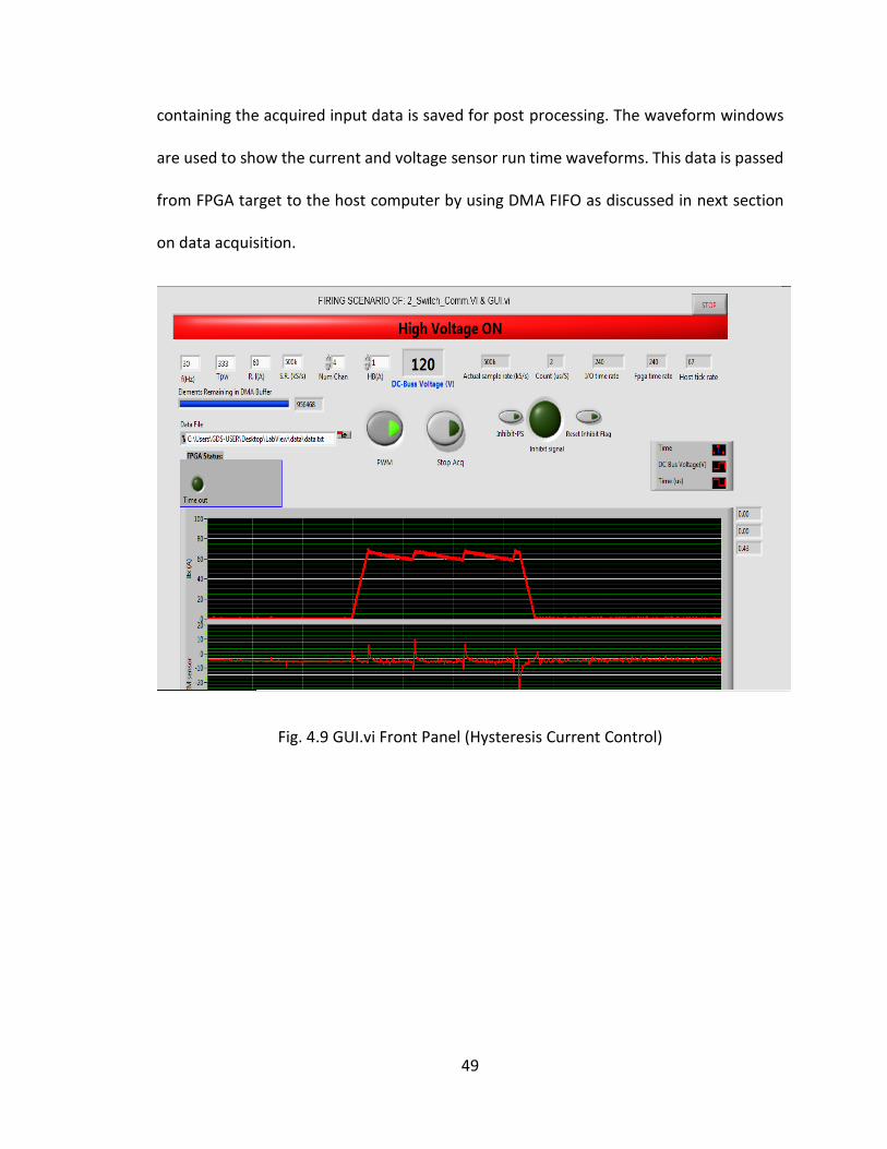
49
containing the acquired input data is saved for post processing. The waveform windows
are used to show the current and voltage sensor run time waveforms. This data is passed
from FPGA target to the host computer by using DMA FIFO as discussed in next section
on data acquisition.
Fig. 4.9 GUI.vi Front Panel (Hysteresis Current Control)
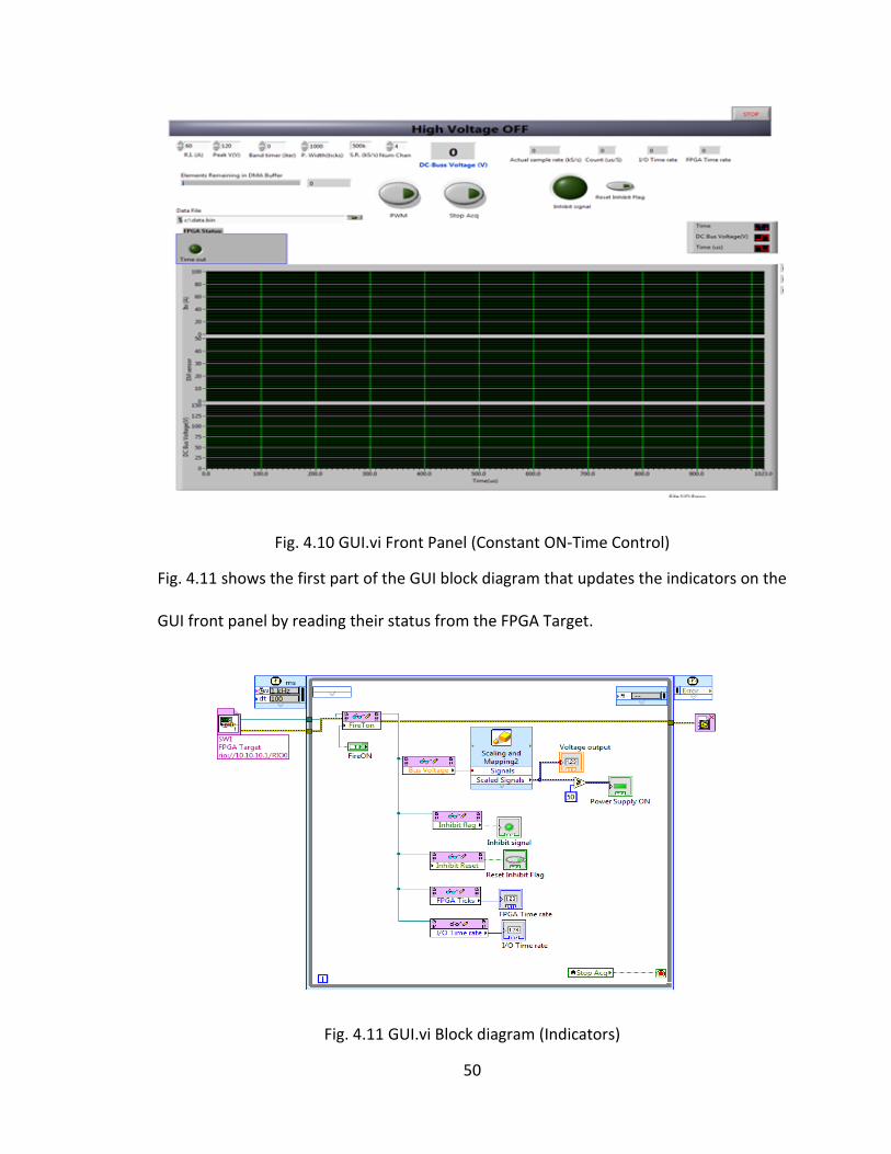
50
Fig. 4.10 GUI.vi Front Panel (Constant ON-Time Control)
Fig. 4.11 shows the first part of the GUI block diagram that updates the indicators on the
GUI front panel by reading their status from the FPGA Target.
Fig. 4.11 GUI.vi Block diagram (Indicators)

51
Fig. 4.12 shows the second part of the GUI block diagram where various control
parameters are passed to the FPGA and also it contains the host side architecture for DMA
FIFO to read the sampled data from analogue input module. The details of data transfer
from FPGA to host are discussed in section 4.5.2
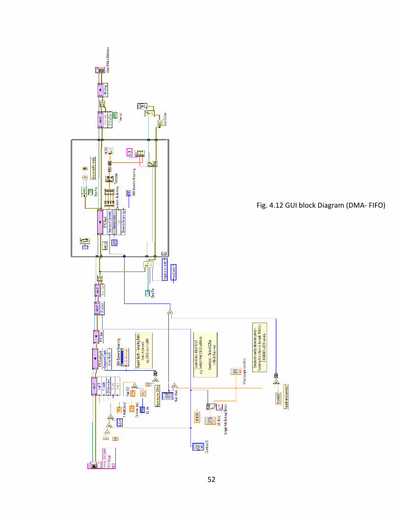
52
Fig. 4.12 GUI block Diagram (DMA- FIFO)

53
4.5.2 FPGA.VI (FPGA TARGET)
FPGA target contains the main code that controls the functioning of power converter.
FPGA code is written in LabVIEW graphical language and is compiled and downloaded to
the FPGA target on the reconfigurable chassis. The FPGA code for this application contains
two major sub parts in terms of two while loops.
Data Acquisition Loop: The first loop as shown in Fig. 4.13 is the Data Acquisition Loop or
DMA FIFO loop where the input data from NI 9222 analogue input module is transferred
to the host machine. There are various ways to read the data from an input module.
However to have a deterministic data reading and transfer from the input module , user-
defined I/O sampling method is described as the best method .By using this method the
maximum sampling rate as high as 500 KS/s can be achieved from an analogue input
module (NI 9222 in this case). Other methods such as using FPGA I/O node results in a
maximum sampling rate of 300 KS/s which results in underutilization of the hardware
components. Fig. 4.14 and Fig. 4.15 shows the general architecture for FPGA I/O node and
user- controlled I/O sampling to read the input module data.
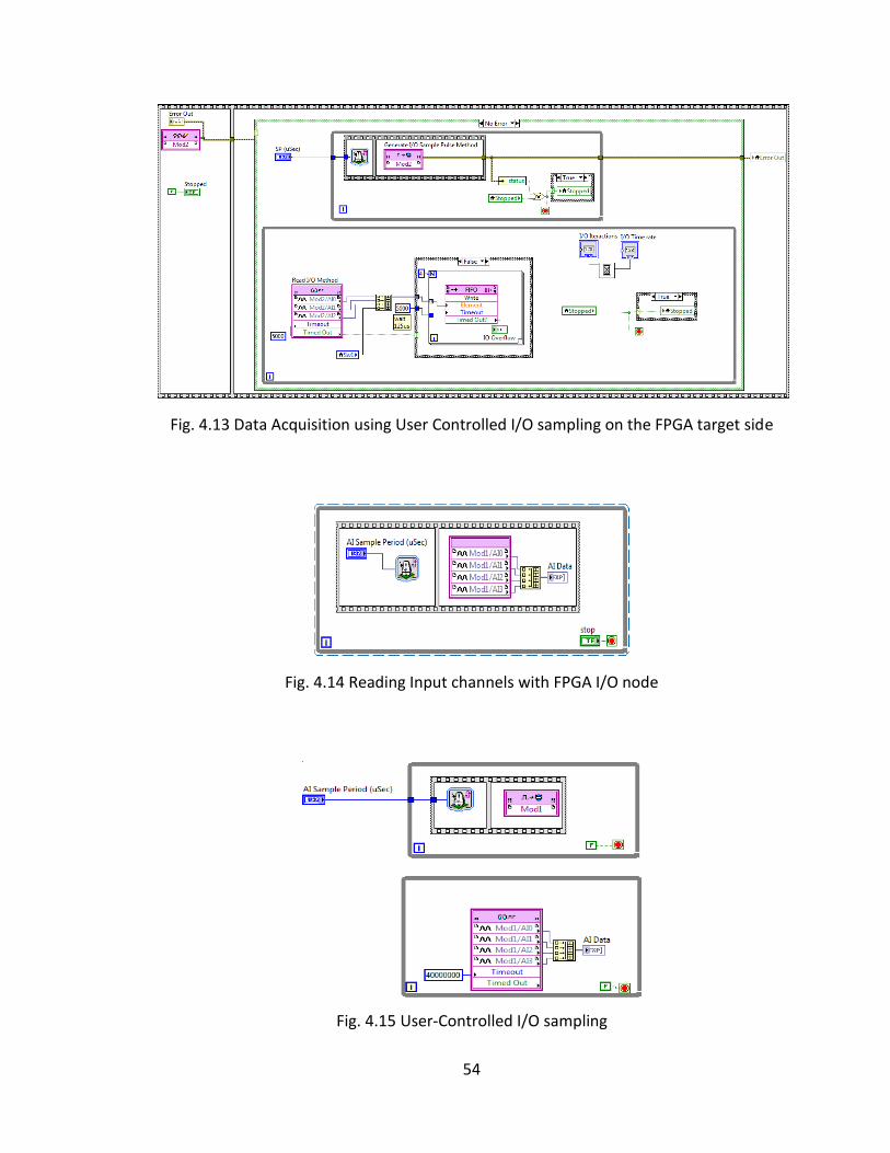
54
Fig. 4.13 Data Acquisition using User Controlled I/O sampling on the FPGA target side
Fig. 4.14 Reading Input channels with FPGA I/O node
Fig. 4.15 User-Controlled I/O sampling

55
The acquired data is transferred from FPGA to the host computer using DMA FIFO (Direct
Memory Access FIFO). This is a special function architecture defined in LabVIEW for
deterministic data transfer between FPGA target and the host computer VI. It consists of
two parts. The first part of this FIFO is on the FPGA target. It uses block RAM on the FPGA
device and is used to read the data from input module. The second part of the DMA FIFO
is on the host machine. This portion of the FIFO uses the host machine memory resources.
Fig. 4.15 shows the data acquisition on the FPGA target side by using user controlled I/O
sampling and DMA FIFO. The analogue input channel data from 3 input channels and a
local variable (containing switch 1 gating signal status) is combined into a single array and
is passed to the FIFO by using “For loop” indexing. The For Loop indexes through each
element of the array and passes the data into a DMA FIFO sequentially with a timeout of
specified ticks (5000 in this case). The second part of the DMA FIFO is on the host side and
is shown in Fig.4.12 in previous section. In Fig. 4.12 the reference to the FPGA is provided
by configuring an open FPGA VI reference function and connecting it to various blocks in
GUI block diagram. The DMA FIFO data is read by starting the DMA FIFO and configuring
a DMA FIFO read node. The read data is in the form of indexed array. A decimate array,
Build array and transpose function is used to make four separate arrays for the read data.
A plot function is used to plot the waveforms on GUI front panel. A write to text file
function is used to write the acquired data into a file on the host computer.
Control Loop: The second loop in the block diagram is the control loop as shown in
Fig. 4.16.The input channel data can be passed from the acquisition loop to the control
loop using different methods such as Local Variable or Real Time FIFOs. However it was

56
found that use of these methods result in the slower execution rates for both the
acquisition and control loops. To avoid any delays in loop execution another User-Defined
I/O node is used in the control loop to read the input channel data. The control loop was
first developed by implementing the digital hysteresis current control by using an inbuilt
LabVIEW function “Relay VI”. It resulted in a loop cycle time of 18 us which is quite high
for current regulation. The loop cycle time is measured in terms of the ticks that a
particular loop takes to execute. For this purpose a sub VI “Timer” was used. The block
diagram for this VI is shown in Fig. 4.17. To measure the execution rate of data acquisition
loop and the control loop this Sub VI is placed separately in these two loops. FPGA ticks
for the data acquisition loop and control loop are passed to the GUI interface as shown in
Fig. 4.11. For a case ,if the FPGA rate shown in the block on GUI displays 240 , it means
the FPGA control loop is taking 240*0.025 =6us per loop cycle. This loop cycle time defines
the actual time step for the control logic. For faster response from the controller it is very
important to keep this time step to minimum which is 2 µs as per the used hardware
capability.
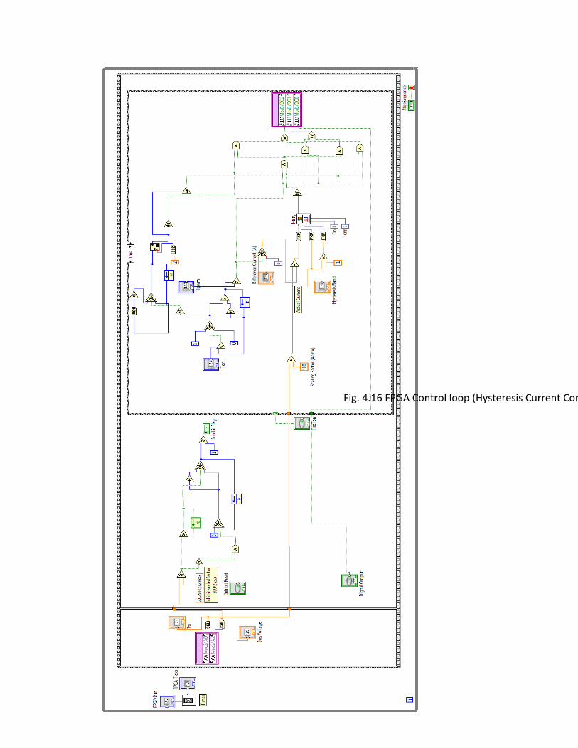
57
Fig. 4.16 FPGA Control loop (Hysteresis Current Control)
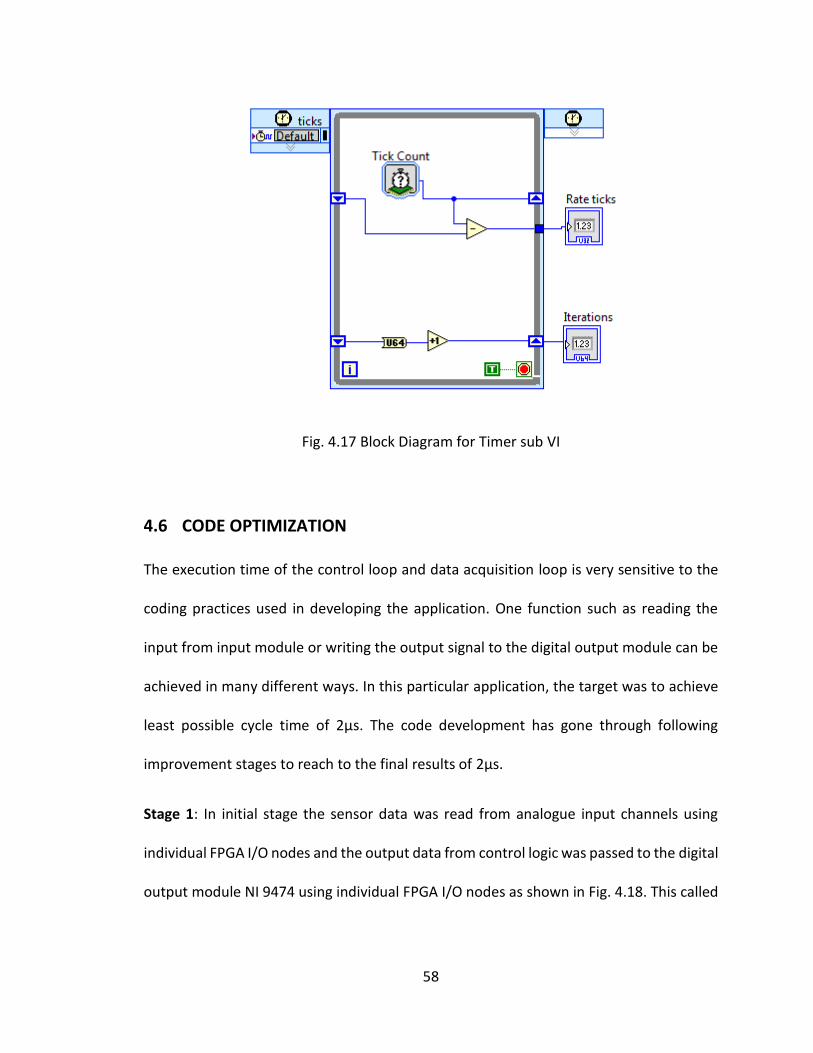
58
Fig. 4.17 Block Diagram for Timer sub VI
4.6 CODE OPTIMIZATION
The execution time of the control loop and data acquisition loop is very sensitive to the
coding practices used in developing the application. One function such as reading the
input from input module or writing the output signal to the digital output module can be
achieved in many different ways. In this particular application, the target was to achieve
least possible cycle time of 2µs. The code development has gone through following
improvement stages to reach to the final results of 2µs.
Stage 1: In initial stage the sensor data was read from analogue input channels using
individual FPGA I/O nodes and the output data from control logic was passed to the digital
output module NI 9474 using individual FPGA I/O nodes as shown in Fig. 4.18. This called
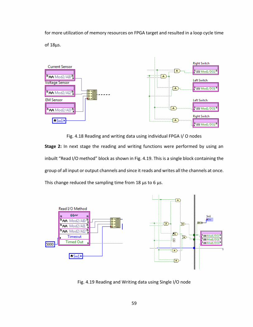
59
for more utilization of memory resources on FPGA target and resulted in a loop cycle time
of 18µs.
Fig. 4.18 Reading and writing data using individual FPGA I/ O nodes
Stage 2: In next stage the reading and writing functions were performed by using an
inbuilt “Read I/O method” block as shown in Fig. 4.19. This is a single block containing the
group of all input or output channels and since it reads and writes all the channels at once.
This change reduced the sampling time from 18 µs to 6 µs.
Fig. 4.19 Reading and Writing data using Single I/O node
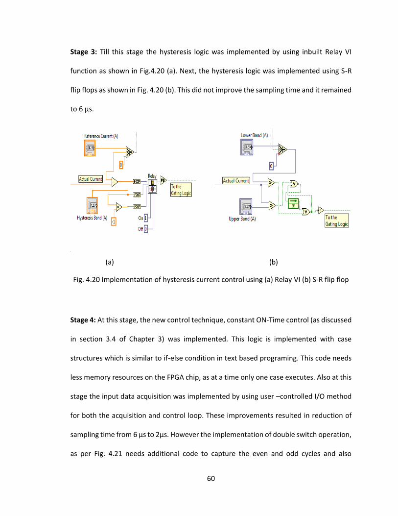
60
Stage 3: Till this stage the hysteresis logic was implemented by using inbuilt Relay VI
function as shown in Fig.4.20 (a). Next, the hysteresis logic was implemented using S-R
flip flops as shown in Fig. 4.20 (b). This did not improve the sampling time and it remained
to 6 µs.
Fi
(a) (b)
Fig. 4.20 Implementation of hysteresis current control using (a) Relay VI (b) S-R flip flop
Stage 4: At this stage, the new control technique, constant ON-Time control (as discussed
in section 3.4 of Chapter 3) was implemented. This logic is implemented with case
structures which is similar to if-else condition in text based programing. This code needs
less memory resources on the FPGA chip, as at a time only one case executes. Also at this
stage the input data acquisition was implemented by using user –controlled I/O method
for both the acquisition and control loop. These improvements resulted in reduction of
sampling time from 6 µs to 2µs. However the implementation of double switch operation,
as per Fig. 4.21 needs additional code to capture the even and odd cycles and also
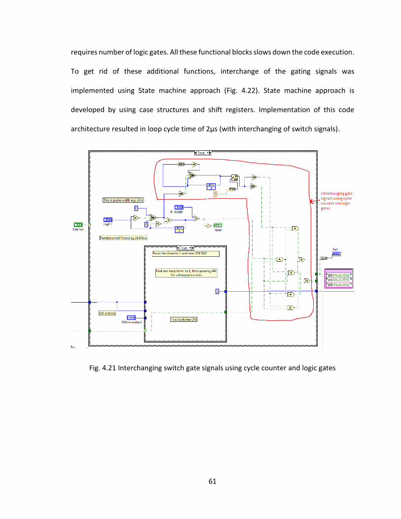
61
requires number of logic gates. All these functional blocks slows down the code execution.
To get rid of these additional functions, interchange of the gating signals was
implemented using State machine approach (Fig. 4.22). State machine approach is
developed by using case structures and shift registers. Implementation of this code
architecture resulted in loop cycle time of 2µs (with interchanging of switch signals).
Fig. 4.21 Interchanging switch gate signals using cycle counter and logic gates
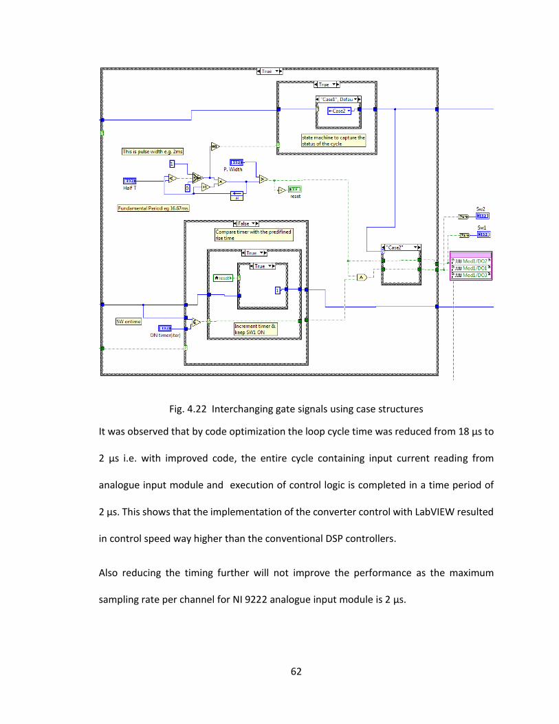
62
Fig. 4.22 Interchanging gate signals using case structures
It was observed that by code optimization the loop cycle time was reduced from 18 µs to
2 µs i.e. with improved code, the entire cycle containing input current reading from
analogue input module and execution of control logic is completed in a time period of
2 µs. This shows that the implementation of the converter control with LabVIEW resulted
in control speed way higher than the conventional DSP controllers.
Also reducing the timing further will not improve the performance as the maximum
sampling rate per channel for NI 9222 analogue input module is 2 µs.
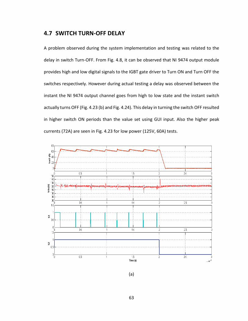
63
4.7 SWITCH TURN-OFF DELAY
A problem observed during the system implementation and testing was related to the
delay in switch Turn-OFF. From Fig. 4.8, it can be observed that NI 9474 output module
provides high and low digital signals to the IGBT gate driver to Turn ON and Turn OFF the
switches respectively. However during actual testing a delay was observed between the
instant the NI 9474 output channel goes from high to low state and the instant switch
actually turns OFF (Fig. 4.23 (b) and Fig. 4.24). This delay in turning the switch OFF resulted
in higher switch ON periods than the value set using GUI input. Also the higher peak
currents (72A) are seen in Fig. 4.23 for low power (125V, 60A) tests.
(a)
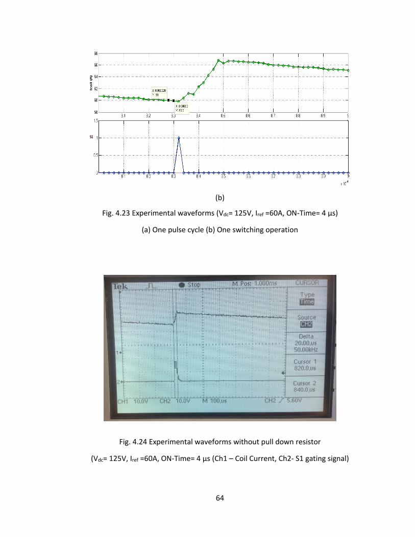
64
(b)
Fig. 4.23 Experimental waveforms (Vdc= 125V, Iref =60A, ON-Time= 4 µs)
(a) One pulse cycle (b) One switching operation
Fig. 4.24 Experimental waveforms without pull down resistor
(Vdc= 125V, Iref =60A, ON-Time= 4 µs (Ch1 – Coil Current, Ch2- S1 gating signal)
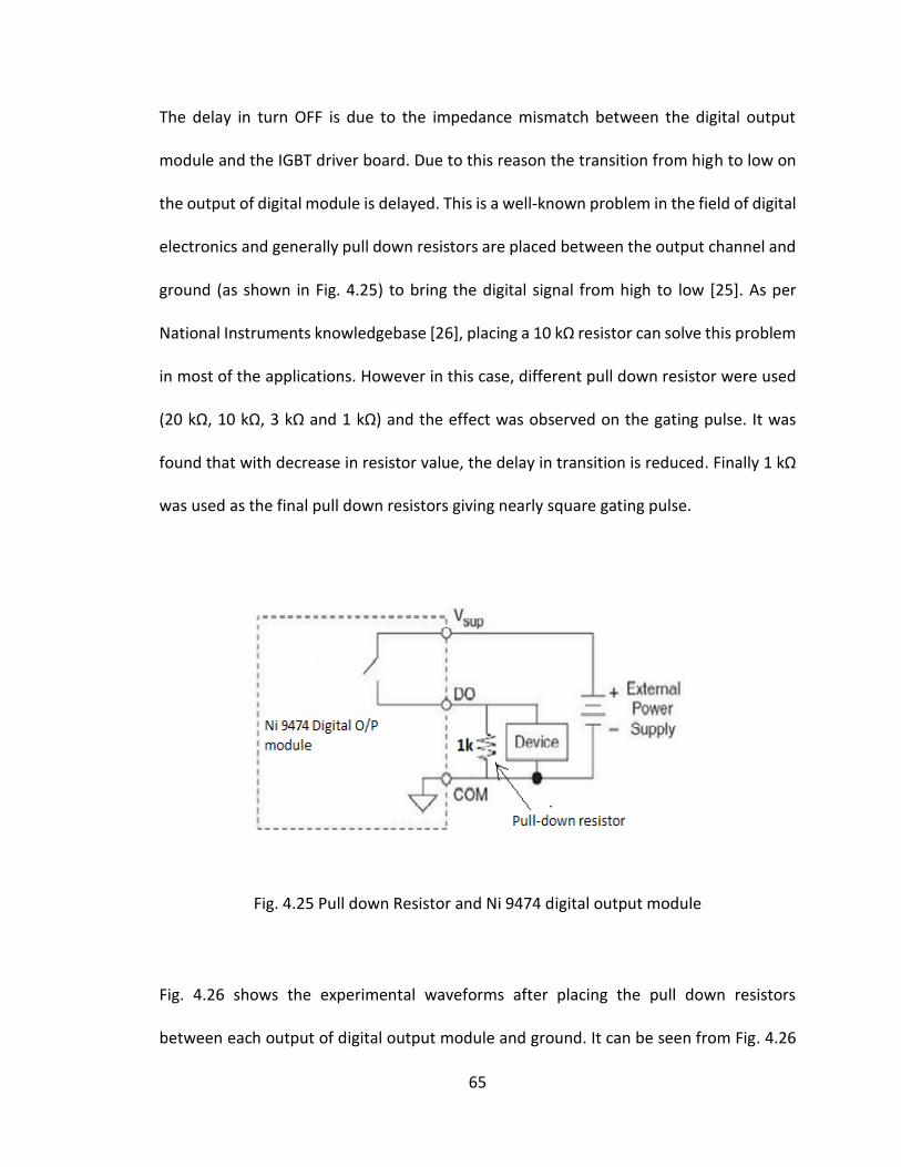
65
The delay in turn OFF is due to the impedance mismatch between the digital output
module and the IGBT driver board. Due to this reason the transition from high to low on
the output of digital module is delayed. This is a well-known problem in the field of digital
electronics and generally pull down resistors are placed between the output channel and
ground (as shown in Fig. 4.25) to bring the digital signal from high to low [25]. As per
National Instruments knowledgebase [26], placing a 10 kΩ resistor can solve this problem
in most of the applications. However in this case, different pull down resistor were used
(20 kΩ, 10 kΩ, 3 kΩ and 1 kΩ) and the effect was observed on the gating pulse. It was
found that with decrease in resistor value, the delay in transition is reduced. Finally 1 kΩ
was used as the final pull down resistors giving nearly square gating pulse.
Fig. 4.25 Pull down Resistor and Ni 9474 digital output module
Fig. 4.26 shows the experimental waveforms after placing the pull down resistors
between each output of digital output module and ground. It can be seen from Fig. 4.26
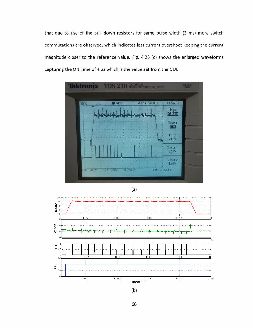
66
that due to use of the pull down resistors for same pulse width (2 ms) more switch
commutations are observed, which indicates less current overshoot keeping the current
magnitude closer to the reference value. Fig. 4.26 (c) shows the enlarged waveforms
capturing the ON Time of 4 µs which is the value set from the GUI.
(a)
(b)
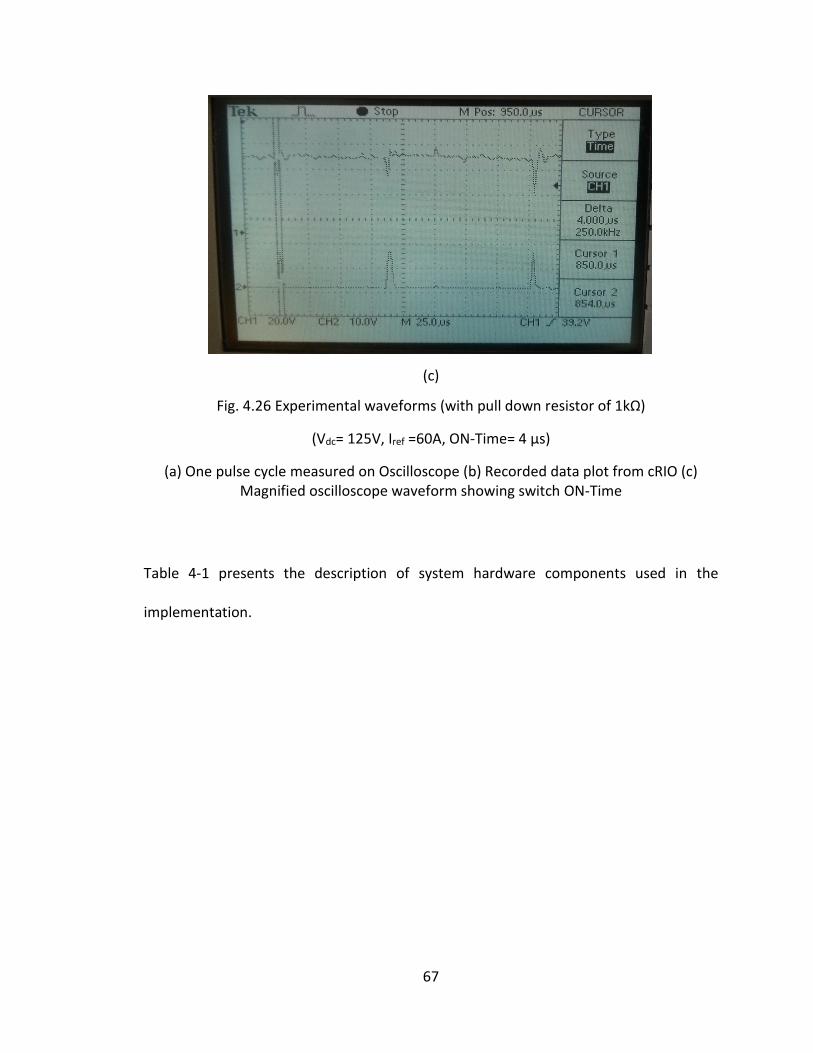
67
(c)
Fig. 4.26 Experimental waveforms (with pull down resistor of 1kΩ)
(Vdc= 125V, Iref =60A, ON-Time= 4 µs)
(a) One pulse cycle measured on Oscilloscope (b) Recorded data plot from cRIO (c) Magnified oscilloscope waveform showing switch ON-Time
Table 4-1 presents the description of system hardware components used in the
implementation.
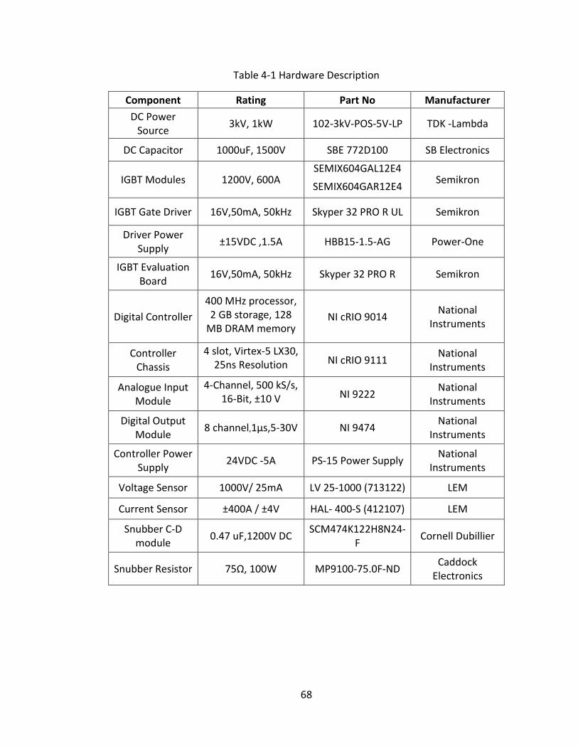
68
Table 4-1 Hardware Description
Component Rating Part No Manufacturer
DC Power Source
3kV, 1kW 102-3kV-POS-5V-LP TDK -Lambda
DC Capacitor 1000uF, 1500V SBE 772D100 SB Electronics
IGBT Modules 1200V, 600A SEMIX604GAL12E4
SEMIX604GAR12E4 Semikron
IGBT Gate Driver 16V,50mA, 50kHz Skyper 32 PRO R UL Semikron
Driver Power Supply
±15VDC ,1.5A HBB15-1.5-AG Power-One
IGBT Evaluation Board
16V,50mA, 50kHz Skyper 32 PRO R Semikron
Digital Controller
400 MHz processor, 2 GB storage, 128
MB DRAM memory NI cRIO 9014
National Instruments
Controller Chassis
4 slot, Virtex-5 LX30, 25ns Resolution NI cRIO 9111
National Instruments
Analogue Input Module
4-Channel, 500 kS/s, 16-Bit, ±10 V
NI 9222 National
Instruments
Digital Output Module
8 channel,1µs,5-30V NI 9474 National
Instruments
Controller Power Supply
24VDC -5A PS-15 Power Supply National
Instruments
Voltage Sensor 1000V/ 25mA LV 25-1000 (713122) LEM
Current Sensor ±400A / ±4V HAL- 400-S (412107) LEM
Snubber C-D module
0.47 uF,1200V DC SCM474K122H8N24-
F Cornell Dubillier
Snubber Resistor 75Ω, 100W MP9100-75.0F-ND Caddock
Electronics
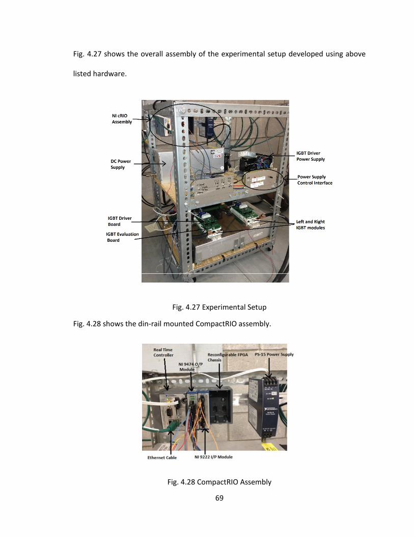
69
Fig. 4.27 shows the overall assembly of the experimental setup developed using above
listed hardware.
Fig. 4.27 Experimental Setup
Fig. 4.28 shows the din-rail mounted CompactRIO assembly.
Fig. 4.28 CompactRIO Assembly
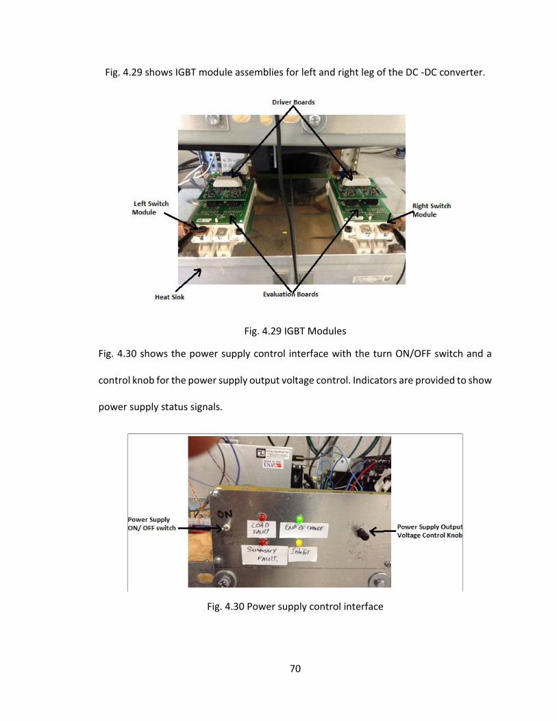
70
Fig. 4.29 shows IGBT module assemblies for left and right leg of the DC -DC converter.
Fig. 4.29 IGBT Modules
Fig. 4.30 shows the power supply control interface with the turn ON/OFF switch and a
control knob for the power supply output voltage control. Indicators are provided to show
power supply status signals.
Fig. 4.30 Power supply control interface

71
4.8 EXPERIMENTAL RESULTS
This section discusses the experimental results obtained from the experimental setup at
desired voltage and current levels. The system waveform data is saved on the host
computer for each test and was plotted in MATLAB Simulink for better representation.
First the system is tested for low DC bus voltage (125 V) and low current (60 A) and setting
the ON-Time to 4 µs. Results with these settings are shown in Fig. 4.31. From Fig. 4.31(a)
it can observed that exact times are achieved for the pulse width (2 ms) and fundamental
period (16.67 ms). The fall time achieved is 110 µs. Switch gating signals interchange
during consecutive cycle is also visible. DC link capacitor voltage is reduced from 125V to
119V by the end of current pulse. The power source supplies the dc current to recharge
the capacitor back to reference voltage in approximately 4.1 ms after the end of the
current pulse. From Fig. 4.31(b) it can be observed that due to low value selected for the
ON-Time, almost constant current is achieved at the top of the current pulse. However
this results in more switch commutations per pulse cycle and hence causes more
switching power loss. The voltage transients are limited effectively by the RCD snubber
modules.
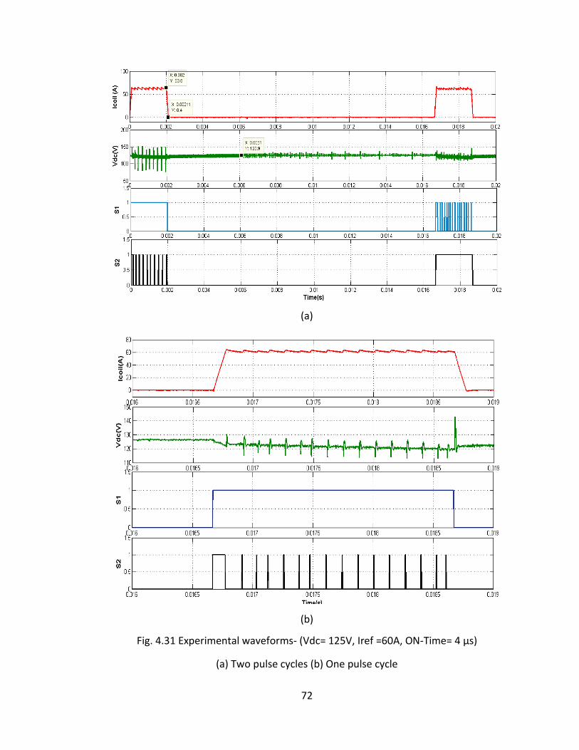
72
(a)
(b)
Fig. 4.31 Experimental waveforms- (Vdc= 125V, Iref =60A, ON-Time= 4 µs)
(a) Two pulse cycles (b) One pulse cycle
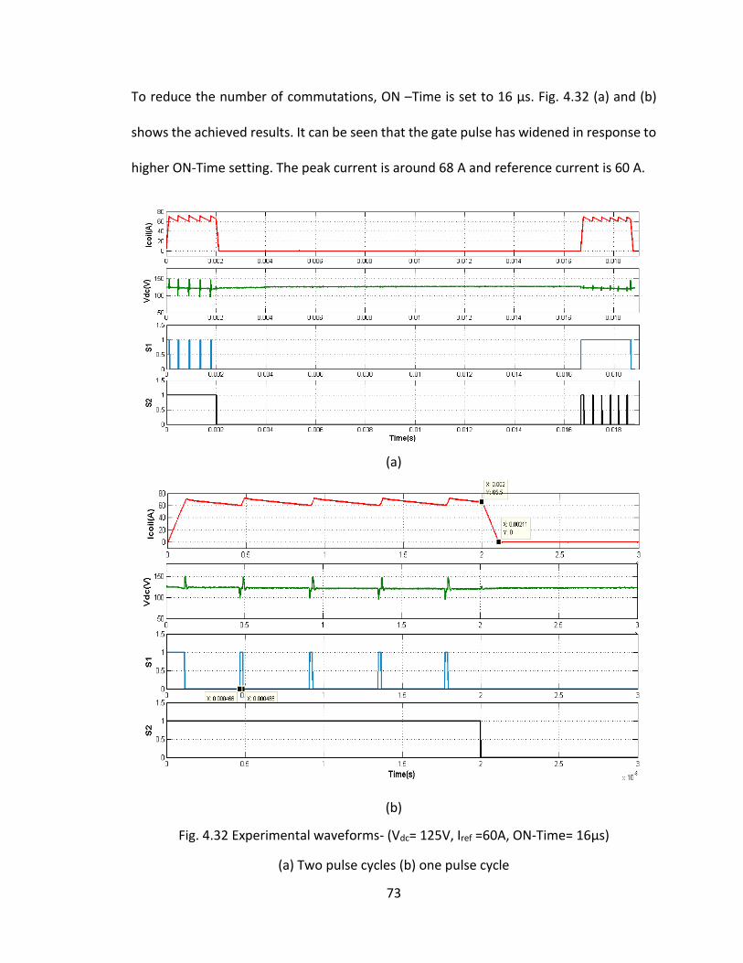
73
To reduce the number of commutations, ON –Time is set to 16 µs. Fig. 4.32 (a) and (b)
shows the achieved results. It can be seen that the gate pulse has widened in response to
higher ON-Time setting. The peak current is around 68 A and reference current is 60 A.
(a)
(b)
Fig. 4.32 Experimental waveforms- (Vdc= 125V, Iref =60A, ON-Time= 16µs)
(a) Two pulse cycles (b) one pulse cycle
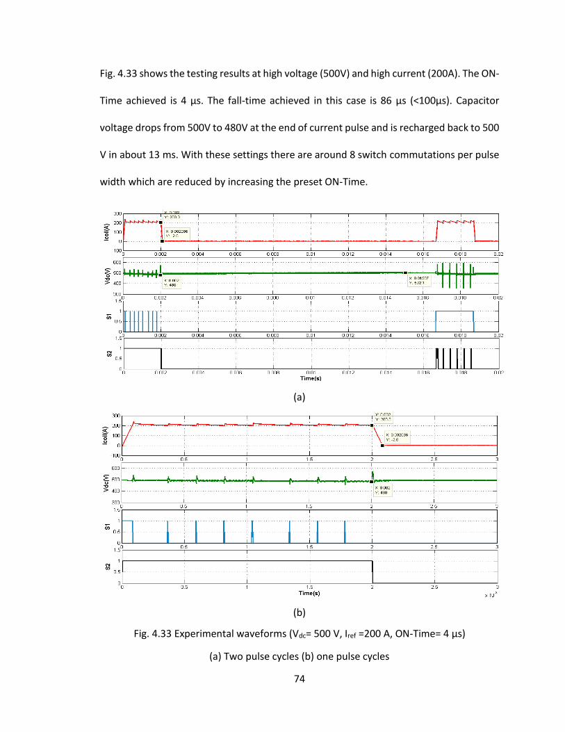
74
Fig. 4.33 shows the testing results at high voltage (500V) and high current (200A). The ON-
Time achieved is 4 µs. The fall-time achieved in this case is 86 µs (<100µs). Capacitor
voltage drops from 500V to 480V at the end of current pulse and is recharged back to 500
V in about 13 ms. With these settings there are around 8 switch commutations per pulse
width which are reduced by increasing the preset ON-Time.
(a)
(b)
Fig. 4.33 Experimental waveforms (Vdc= 500 V, Iref =200 A, ON-Time= 4 µs)
(a) Two pulse cycles (b) one pulse cycles
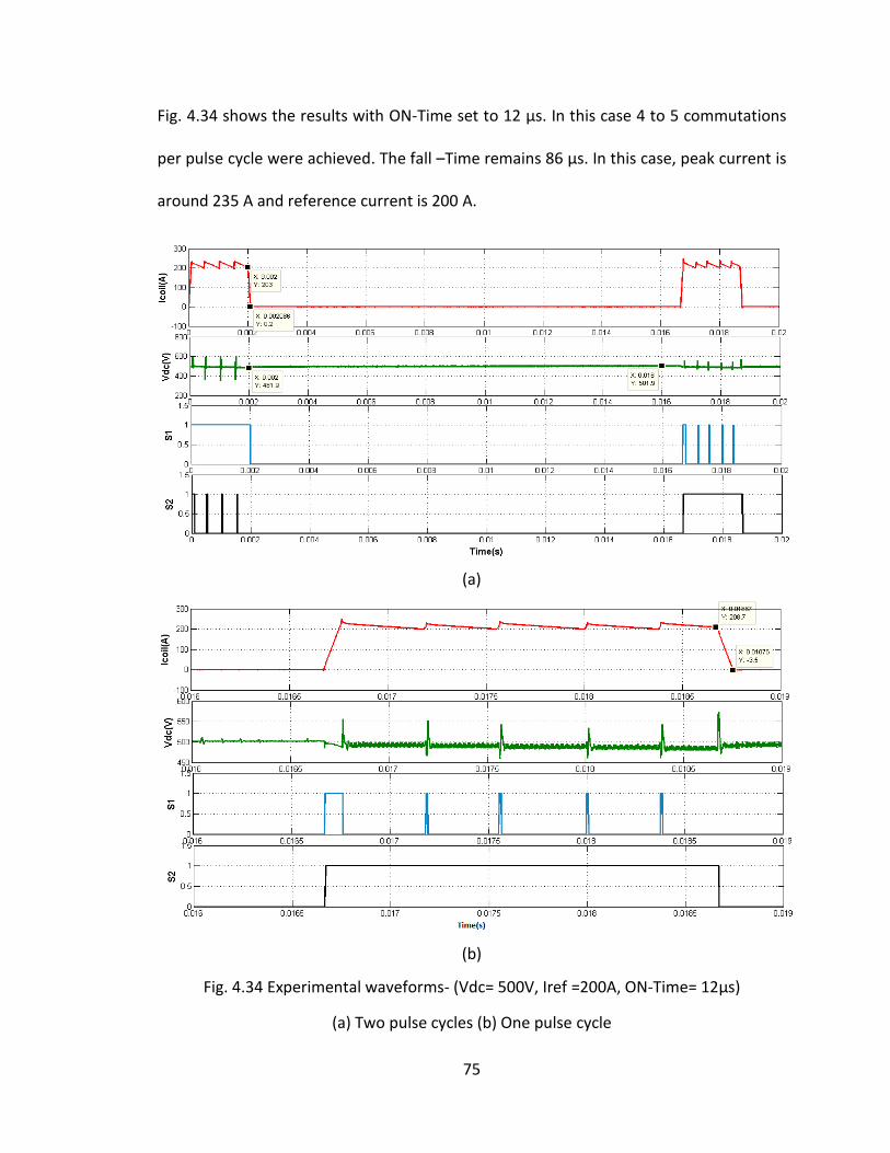
75
Fig. 4.34 shows the results with ON-Time set to 12 µs. In this case 4 to 5 commutations
per pulse cycle were achieved. The fall –Time remains 86 µs. In this case, peak current is
around 235 A and reference current is 200 A.
(a)
(b)
Fig. 4.34 Experimental waveforms- (Vdc= 500V, Iref =200A, ON-Time= 12µs)
(a) Two pulse cycles (b) One pulse cycle
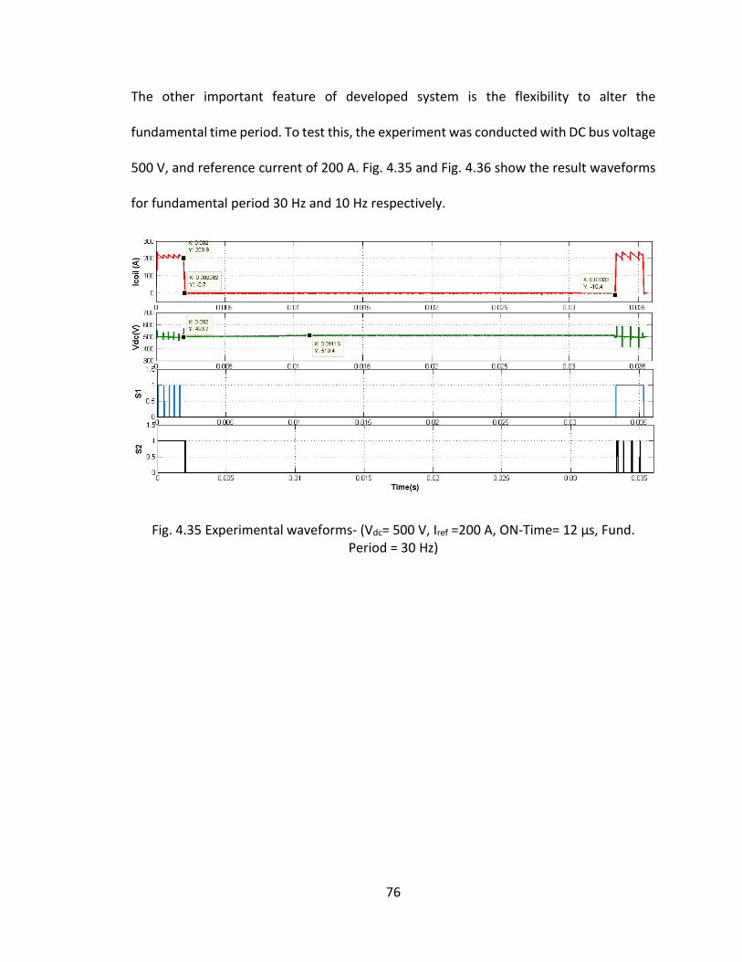
76
The other important feature of developed system is the flexibility to alter the
fundamental time period. To test this, the experiment was conducted with DC bus voltage
500 V, and reference current of 200 A. Fig. 4.35 and Fig. 4.36 show the result waveforms
for fundamental period 30 Hz and 10 Hz respectively.
Fig. 4.35 Experimental waveforms- (Vdc= 500 V, Iref =200 A, ON-Time= 12 µs, Fund. Period = 30 Hz)
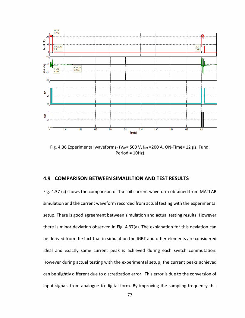
77
Fig. 4.36 Experimental waveforms- (Vdc= 500 V, Iref =200 A, ON-Time= 12 µs, Fund. Period = 10Hz)
4.9 COMPARISON BETWEEN SIMAULTION AND TEST RESULTS
Fig. 4.37 (c) shows the comparison of T-x coil current waveform obtained from MATLAB
simulation and the current waveform recorded from actual testing with the experimental
setup. There is good agreement between simulation and actual testing results. However
there is minor deviation observed in Fig. 4.37(a). The explanation for this deviation can
be derived from the fact that in simulation the IGBT and other elements are considered
ideal and exactly same current peak is achieved during each switch commutation.
However during actual testing with the experimental setup, the current peaks achieved
can be slightly different due to discretization error. This error is due to the conversion of
input signals from analogue to digital form. By improving the sampling frequency this
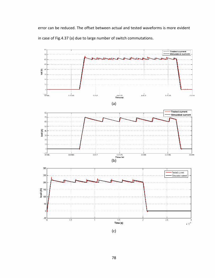
78
error can be reduced. The offset between actual and tested waveforms is more evident
in case of Fig.4.37 (a) due to large number of switch commutations.
(a)
(b)
(c)
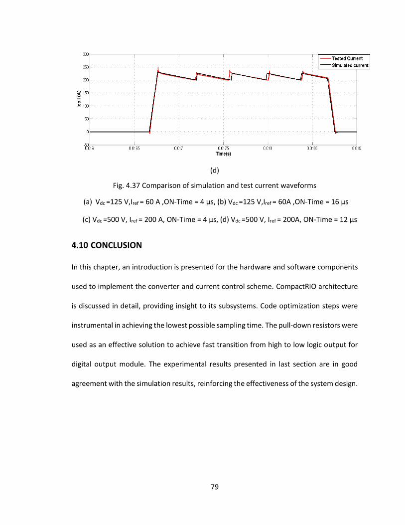
79
(d)
Fig. 4.37 Comparison of simulation and test current waveforms
(a) Vdc =125 V,Iref = 60 A ,ON-Time = 4 µs, (b) Vdc =125 V,Iref = 60A ,ON-Time = 16 µs
(c) Vdc =500 V, Iref = 200 A, ON-Time = 4 µs, (d) Vdc =500 V, Iref = 200A, ON-Time = 12 µs
4.10 CONCLUSION
In this chapter, an introduction is presented for the hardware and software components
used to implement the converter and current control scheme. CompactRIO architecture
is discussed in detail, providing insight to its subsystems. Code optimization steps were
instrumental in achieving the lowest possible sampling time. The pull-down resistors were
used as an effective solution to achieve fast transition from high to low logic output for
digital output module. The experimental results presented in last section are in good
agreement with the simulation results, reinforcing the effectiveness of the system design.

80
CHAPTER 5. ZERO CURRENT SWITCHING CONVERTER DESIGN
5.1 INTRODUCTION
All IGBT based converter topologies involve two basic types of power losses i.e.
conduction losses and the switching losses. Conduction losses mainly depend on the
current passing through a switch, ON state voltage drop and the conduction time.
Switching losses are the losses incurred due to the current and voltage transitions across
the IGBT at the time of turn ON and turn OFF process. The switching losses mainly depend
on the current and voltage magnitude, the turn ON and turn OFF speed of the IGBT and
the switching frequency. At high switching frequencies the switching losses are generally
higher than the conduction losses. In order to reduce the overall power loss in the IGBTs,
soft switching techniques are widely used [27]. Although there are variety of
configurations used in soft switching techniques, but most basic techniques are Zero
Current Switching (ZCS) and Zero Voltage Switching (ZVS).
5.2 NEED FOR SOFT SWITCHING
Soft switching is basically used in power converters to reduce the switching losses in
power converters. Before selecting a soft switching technique for the hard switching
converter, it is important to calculate the conduction and switching losses in the hard
switching converter. The power loss is mainly calculated for the switches and the diodes.
Power loss in other components remain essentially constant and is not considered in
these calculations. Previous literature [28] [29] show the method for calculation of IGBT
power loss using datasheet parameters.

81
Turn-ON and Turn –OFF gate resistors have great effect on the switching speed of the
IGBT. Hence it is important to calculate the accurate Turn-ON and Turn –OFF resistor
values. The calculation of gate resistor is shown in Appendix A-1.The detailed power loss
calculations for the hard switching are shown in Appendix A -2. It can be observed that by
switch S1 switching power loss is 37% of the total power loss and an effective soft
switching scheme can minimize these losses. Hence, the implementation of soft switching
converter will help in reduction in power loss and the size of heat sinks can be reduced.
5.3 SELECTION BETWEEN ZCS AND ZVS
Zero Voltage Switching (ZVS) and Zero Current Switching (ZCS) techniques reduce the
switching power loss by bringing the voltage and/ or current across the switch to zero at
the time of commutation from ON to OFF state and vice versa. The basic requirement for
ZVS is that the switch OFF period should correspond to the resonant half cycle time period
of the circuit. On the other hand, in the case of ZCS, switch ON period should correspond
to the resonant half cycle time period of the circuit. In the proposed topology due to sharp
rise in current during ON period and slow decay of current during OFF period, a relatively
shorter ON time period than OFF time period is expected. Also the resonance half period
is given by
𝑇𝑟 = √𝐿𝑟∗𝐶𝑟
2 (5.1)
Where Lr= Resonance Inductor and Cr = Resonance Capacitor
As per equation (5.1), use of ZVS needs bigger resonance elements in order to meet the
soft switching requirements, however on other side ZCS can be implemented with smaller

82
resonance elements as resonance half period correspond to the ON time period. Hence
in this work, ZCS is preferred choice for soft switching operation of the proposed
converter.
5.4 ZCS SOFT SWITCHING CONVERTER TOPOLOGY
The current control for the converter operation is achieved by keeping one of the switch
ON for the period of current pulse and the other switch commutates at high frequency.
The circuit behavior during these modes is similar to a buck converter operation. Hence
the zero current switching techniques developed for buck converters [31] can be utilized.
To achieve zero current switching, an inductor is placed in series with the switch and a
capacitor is placed in parallel with the freewheeling diode FWD1 as shown in Fig. 5.1.
To implement the soft switching, only one switch operation is considered where switch
S1 operates at high frequency and switch S2 remains closed for the time of Pulse Width
(2ms). Also if the ZCS is implemented, the need for alternate switch operation is
eliminated as the thermal stress on the switches will come down.
Fig. 5.1 (a) shows the proposed converter with zero current switching. In a simple zero
current switching topology, a resonant inductor is placed in series with the switch and a
resonant capacitor is placed in parallel to the freewheeling diode (as shown in Fig.5.1 (a))
5.4.1 MODES OF OPERATION (SOFT SWITCHING)
With soft switching (ZCS), the converter modes of operation during constant ON -Time
control is shown in Figure 5.1(b) to 5.1(f) and the corresponding waveforms are shown in
Fig. 5.2. To discuss the following modes of operations it is considered that the current
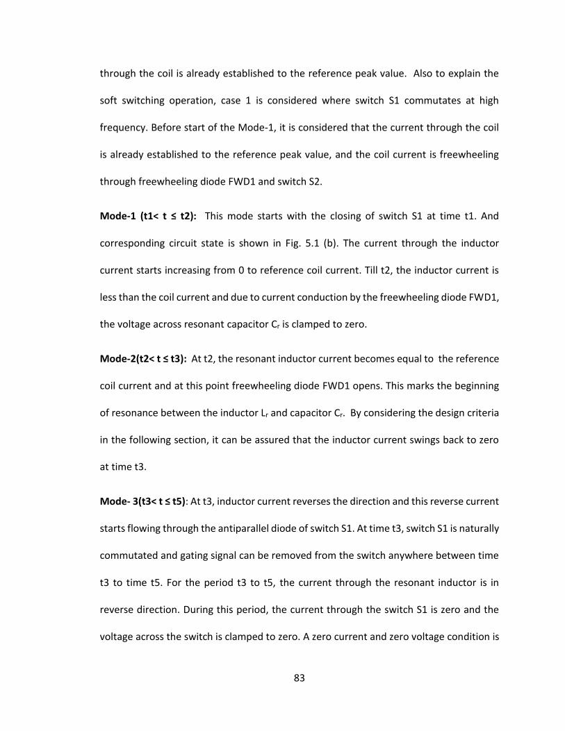
83
through the coil is already established to the reference peak value. Also to explain the
soft switching operation, case 1 is considered where switch S1 commutates at high
frequency. Before start of the Mode-1, it is considered that the current through the coil
is already established to the reference peak value, and the coil current is freewheeling
through freewheeling diode FWD1 and switch S2.
Mode-1 (t1< t ≤ t2): This mode starts with the closing of switch S1 at time t1. And
corresponding circuit state is shown in Fig. 5.1 (b). The current through the inductor
current starts increasing from 0 to reference coil current. Till t2, the inductor current is
less than the coil current and due to current conduction by the freewheeling diode FWD1,
the voltage across resonant capacitor Cr is clamped to zero.
Mode-2(t2< t ≤ t3): At t2, the resonant inductor current becomes equal to the reference
coil current and at this point freewheeling diode FWD1 opens. This marks the beginning
of resonance between the inductor Lr and capacitor Cr. By considering the design criteria
in the following section, it can be assured that the inductor current swings back to zero
at time t3.
Mode- 3(t3< t ≤ t5): At t3, inductor current reverses the direction and this reverse current
starts flowing through the antiparallel diode of switch S1. At time t3, switch S1 is naturally
commutated and gating signal can be removed from the switch anywhere between time
t3 to time t5. For the period t3 to t5, the current through the resonant inductor is in
reverse direction. During this period, the current through the switch S1 is zero and the
voltage across the switch is clamped to zero. A zero current and zero voltage condition is

84
created at the turn OFF of the switch S1. At t5, the current through diode goes to zero
and cannot reverse direction as the gating signal for switch S1 is already removed. This
marks the end of mode 3.
Mode - 4(t5< t ≤ t6): At time t5 inductor current is zero but there is still some positive
voltage across resonant capacitor Cr. The coil current flows through the capacitor
discharging it linearly to zero voltage at time t6.
Mode- 5(t > t6): Beyond t6, the freewheeling diode FWD1, is forward biased and starts
carrying the coil current. In this phase zero voltage is applied across the transmitter coil.
So the current starts decreasing due to the resistance of the elements in the current path
until the reference coil current is reached. At this point, the switch S1 is closed at zero
current and the mode -1 through mode -5 are repeated.
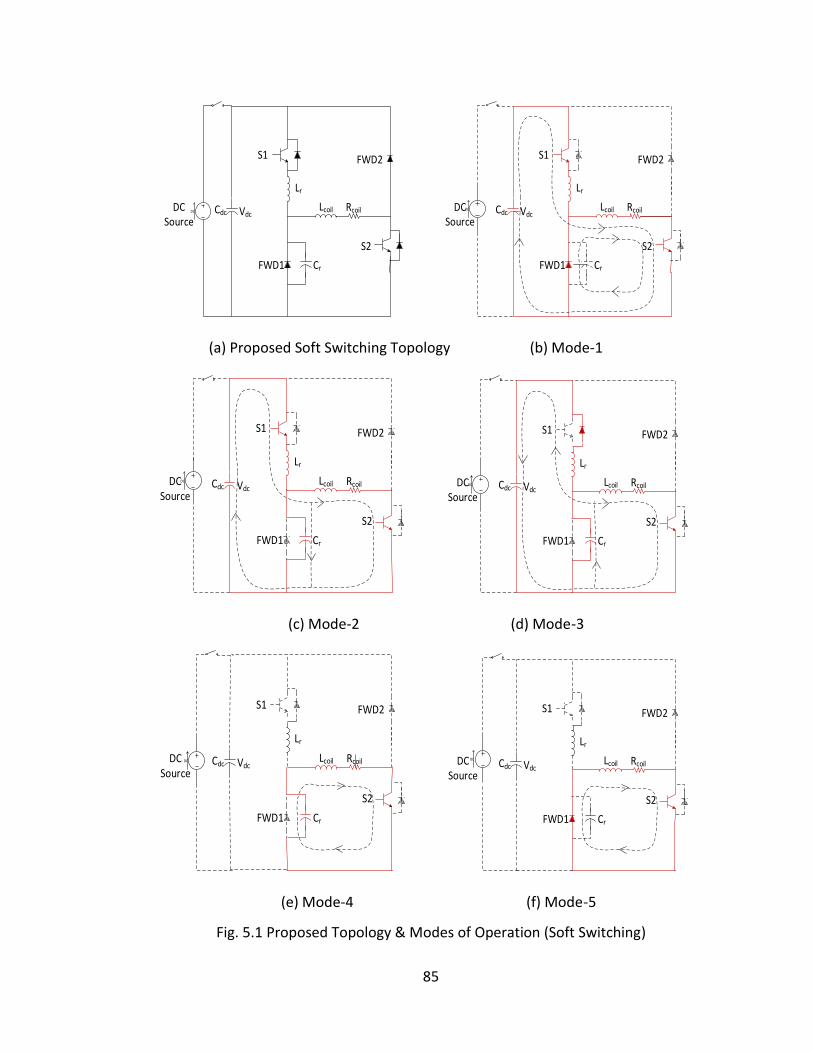
85
VdcLcoil
S2
S1
FWD1
FWD2
RcoilCdcDC
Source
Lr
Cr
DC
VdcLcoil
S2
S1
FWD1
FWD2
RcoilCdcDC
Source
Lr
Cr
DC
(a) Proposed Soft Switching Topology (b) Mode-1
VdcLcoil
S2
S1
FWD1
FWD2
RcoilCdcDC
Source
Lr
Cr
DC
VdcLcoil
S2
S1
FWD1
FWD2
RcoilCdcDC
Source
Lr
Cr
DC
(c) Mode-2 (d) Mode-3
VdcLcoil
S2
S1
FWD1
FWD2
RcoilCdcDC
Source
Lr
Cr
DC
VdcLcoil
S2
S1
FWD1
FWD2
RcoilCdcDC
Source
Lr
Cr
DC
(e) Mode-4 (f) Mode-5
Fig. 5.1 Proposed Topology & Modes of Operation (Soft Switching)
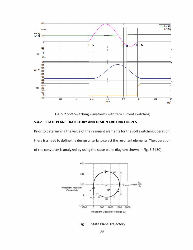
86
Fig. 5.2 Soft Switching waveforms with zero current switching
5.4.2 STATE PLANE TRAJECTORY AND DESIGN CRITERIA FOR ZCS
Prior to determining the value of the resonant elements for the soft switching operation,
there is a need to define the design criteria to select the resonant elements. The operation
of the converter is analyzed by using the state plane diagram shown in Fig. 5.3 [30].
Fig. 5.3 State Plane Trajectory

87
The equations for inductor voltage and capacitor current for various modes are given as
Mode1: In this mode, Inductor current increases linearly from zero to the reference coil
current value. Following relationship relates the DC bus voltage with the rate of change
of current through the resonant inductor [31].
𝑉𝑑𝑐 = 𝐿𝑟𝐼𝑟𝑒𝑓
𝑡2−𝑡1 (5.2)
Rearranging equation (5.2),
𝑇𝑎 = 𝑡2 − 𝑡1 = 𝐿𝑟𝐼𝑟𝑒𝑓
𝑉𝑑𝑐 (5.3)
Ta represents the initial rise time for the current through the resonant inductor
Mode2: In mode 2, inductor Lr and capacitor Cr resonates. During resonance, The
Instantaneous resonant inductor current is given by [31]
𝑖𝐿𝑟 = 𝐼𝑟𝑒𝑓 +𝑉𝑑𝑐
𝑍𝑟sin(𝜔𝑟𝑡) (5.4)
Where Iref = Reference coil current
Vdc = DC bus Capacitor voltage
𝑍𝑟 = √𝐿𝑟
𝐶𝑟
𝜔𝑟 =1
√𝐿𝑟𝐶𝑟
And instantaneous capacitor voltage is given by [31]
𝑣𝑐𝑟 = 𝑉𝑑𝑐 (1 − cos(𝜔𝑟𝑡)) (5.5)

88
From Fig. 5.3 it can be seen that the mode2 ends when the inductor current reaches 0A.
Putting iLr=0, in equation (5.4), [31]
𝑇𝑏 = 𝑡3 − 𝑡2 =𝜋+sin−1(
𝐼𝑟𝑒𝑓𝑍𝑟
𝑉𝑑𝑐)
𝜔𝑟 (5.6)
Mode3: In mode 3, the inductor current flows through antiparallel diode and time t5-t2
is given by [31]
𝑇𝑐 = 𝑡5 − 𝑡2 =2𝜋−sin−1(
𝐼𝑟𝑒𝑓𝑍𝑟
𝑉𝑑𝑐)
𝜔𝑟 (5.7)
Mode 4: In this mode, the resonant capacitor discharges linearly and the time for this
mode t6 –t5 is given by [31]
𝑇𝑑 = 𝑡6 − 𝑡5 = 𝐶𝑟
𝑉𝑑𝑐 (1−cos (sin−1(𝐼𝑟𝑒𝑓𝑍𝑟
𝑉𝑑𝑐))
𝐼𝑟𝑒𝑓 (5.8)
The major design criteria that should be met for an optimized design is as follows
1. The resonant inductor Lr and resonant capacitor Cr shall be selected in a way that
the instant at which the gating signal is removed from the switch, occurs when the
antiparallel diode is conducting the reverse current.
2. The average value of coil current Iref must be less than the state space circle radius
i.e. 𝑉𝑑𝑐
Zr.
In other words, the condition𝑍𝑟 <𝑉𝑑𝑐
𝐼ref shall be satisfied to bring the switch
current to zero during each cycle.
Here 𝑍𝑟 = √𝐿𝑟
𝐶𝑟 ,

89
Lr = Resonant Inductor and Cr = Resonant Capacitor
3. The peak value of current through the resonant inductor and switch is given by
𝐼𝐿𝑟,𝑝𝑒𝑎𝑘 = 𝐼𝑟𝑒𝑓 +𝑉𝑑𝑐
𝑍𝑟 (5.9)
Here in order to keep the 𝐼𝐿𝑟,𝑝𝑒𝑎𝑘to a minimum value, the resonant impedance Zr
shall be kept maximum possible (in accordance with criteria 2)
5.4.3 DESIGN CALCULATIONS
To design Lr and Cr, high voltage (Vdc =500V) and high current (Icoil=200A) was considered.
The ON period for the switch is selected as 12µs.
As per the design criteria discussed in previous section,
Ta + Tb ≤ 12 µs ≤ Ta + Tc (5.10)
Also, within one pulse operation, the DC bus voltage is subject to decrease due to losses
in the circuit. In case of hysteresis current control, with decrease in DC bus voltage the
rate of rise of coil current is effected resulting in variable ON time for the switch. However
in case of Constant ON- Time control, ON –Time for the switch is independent of the DC
bus voltage magnitude. Hence the designed value of resonant elements Lr and Cr provides
effective soft switching. To select the rating for Lr and Cr, one of the element rating is fixed
and then the value of other element is calculated using the above stated equations so
that the design criteria is fulfilled. An iterative approach was followed to reach at the final
values of Lr and Cr, while adhering to the design criteria.
Now as per design criteria for ZCS, 𝑍𝑟 <𝑉𝑑𝑐
𝐼𝑟𝑒𝑓 = 2.5

90
Zr equal to 2.5 is a boundary condition and it implies that Tb= Tc. There will be only one
instant at which current through the switch is zero. On the other hand if Zr is less than 2.5
a time period “Tc-Tb” is achieved where the current through the switch is zero. Also, Zr
can’t be too low as it will result in very high current peaks through the switch and resonant
inductor as per equation (5.9).
Hence a Zr = 1.8 was considered to be a reasonably good value for this design.
To start Cr =1.2 µF was considered and by putting value of Cr in following expression, Lr is
calculated
√𝐿𝑟
𝐶𝑟= 1.8
Lr = 3.9 µF
Putting Lr =3.9 µH, Cr = 1.2 µF, Zr =1.8, ωr = 4.62x10⁵ rad/s, in Equation (5.3), (5.6), (5.7),
(5.8) and (5.9) Ta = 1.56 µs, Tb= 8.54 µs, Tc = 11.9 µs
Ta + Tb = 10.1 µs and Ta + Tc = 13.46 µs
The complete design summary is given in Table 5-1
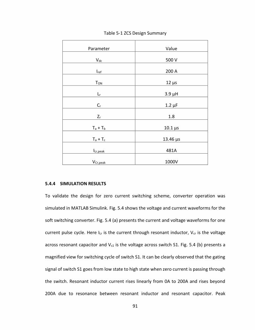
91
Table 5-1 ZCS Design Summary
Parameter Value
Vdc 500 V
Iref 200 A
TON 12 µs
Lr 3.9 µH
Cr 1.2 µF
Zr 1.8
Ta + Tb 10.1 µs
Ta + Tc 13.46 µs
ILr,peak 481A
VCr,peak 1000V
5.4.4 SIMULATION RESULTS
To validate the design for zero current switching scheme, converter operation was
simulated in MATLAB Simulink. Fig. 5.4 shows the voltage and current waveforms for the
soft switching converter. Fig. 5.4 (a) presents the current and voltage waveforms for one
current pulse cycle. Here ILr is the current through resonant inductor, Vcr is the voltage
across resonant capacitor and Vs1 is the voltage across switch S1. Fig. 5.4 (b) presents a
magnified view for switching cycle of switch S1. It can be clearly observed that the gating
signal of switch S1 goes from low state to high state when zero current is passing through
the switch. Resonant inductor current rises linearly from 0A to 200A and rises beyond
200A due to resonance between resonant inductor and resonant capacitor. Peak
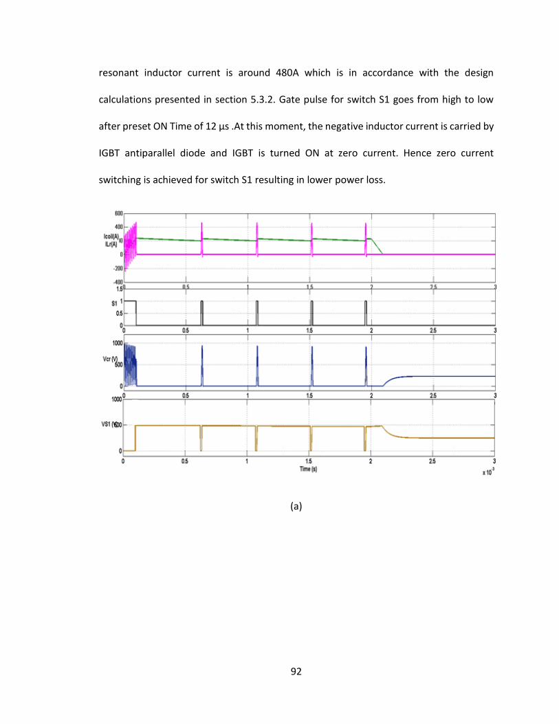
92
resonant inductor current is around 480A which is in accordance with the design
calculations presented in section 5.3.2. Gate pulse for switch S1 goes from high to low
after preset ON Time of 12 µs .At this moment, the negative inductor current is carried by
IGBT antiparallel diode and IGBT is turned ON at zero current. Hence zero current
switching is achieved for switch S1 resulting in lower power loss.
(a)
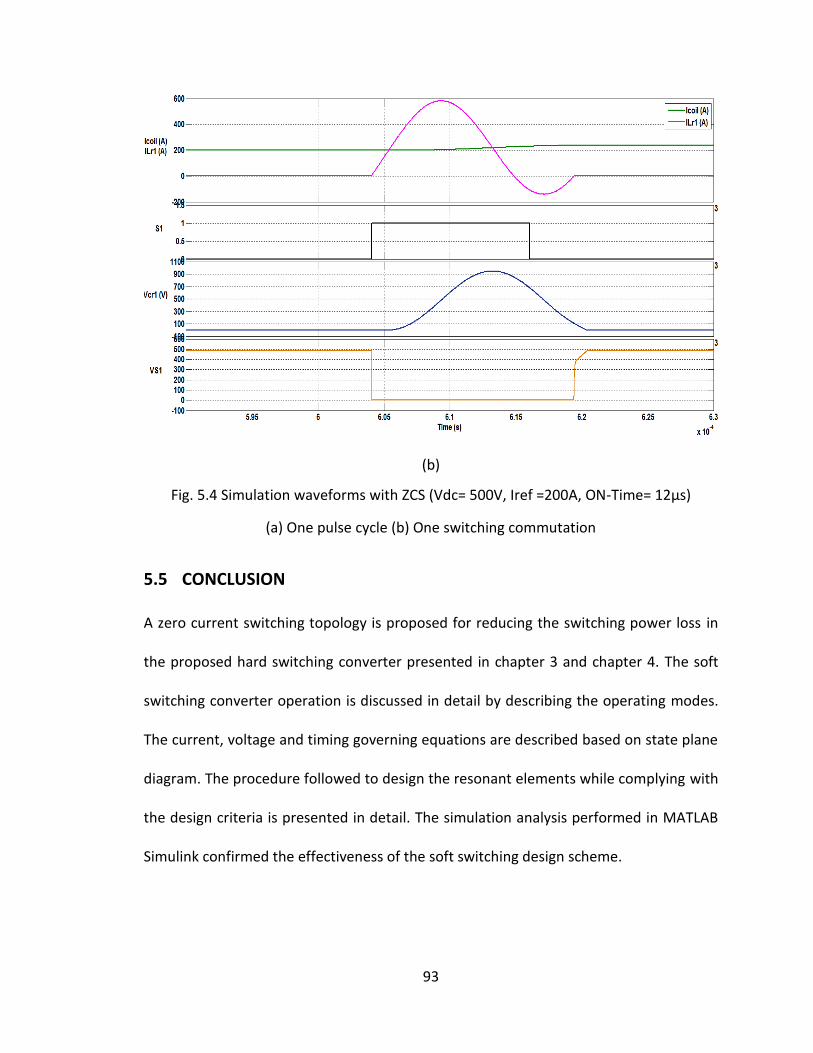
93
(b)
Fig. 5.4 Simulation waveforms with ZCS (Vdc= 500V, Iref =200A, ON-Time= 12µs)
(a) One pulse cycle (b) One switching commutation
5.5 CONCLUSION
A zero current switching topology is proposed for reducing the switching power loss in
the proposed hard switching converter presented in chapter 3 and chapter 4. The soft
switching converter operation is discussed in detail by describing the operating modes.
The current, voltage and timing governing equations are described based on state plane
diagram. The procedure followed to design the resonant elements while complying with
the design criteria is presented in detail. The simulation analysis performed in MATLAB
Simulink confirmed the effectiveness of the soft switching design scheme.

94
CHAPTER 6. CONCLUSION AND FUTURE WORK
6.1 SUMMARY
The thesis describes the design and implementation of a high power converter topology
to provide high current pulses in a time domain electromagnetic system. The proposed
system is designed with an objective to develop a compact yet high power system,
capable of controlling the current pulse through the transmitter coil (Tx- coil).
A LabVIEW based CompactRIO hardware platform was implemented to achieve a faster
digital current control. A constant ON-Time current control concept is devised and
implemented to achieve better control on switch ON times and to have better current
regulation. Current fall time less than 100 µs was achieved with a sampling frequency of
500 kHz. The short fall times and high current magnitude achieved are important to
achieve higher secondary field response from the mineral target.
Code optimization techniques, are described in detail which were instrumental in
reducing the sampling time to 2 µs. Also high sampling frequency achieved helps to
improve the accuracy and resolution of the survey data, providing more data points per
fundamental period. The development of graphical user interface on the host computer
provides the user with the flexibility to control various parameters such as pulse width
and fundamental frequency of the current pulse.
The simulation and experimental results proved the effectiveness of the proposed system
and the current control scheme. In the end, a zero current switching scheme is proposed
to reduce the switching power loss in the power converter. The design approach for

95
selecting the resonant elements was presented in detail. The simulated results proved
the effectiveness of the proposed soft switching scheme and verified the design of
resonant elements.
6.2 SUGGESTED FUTURE WORK
1. In this work only unipolar current pulses were implemented. In the next level of
development, bipolar current pulses can be implemented using full bridge
converter. Bipolar current pulses provides the benefit of automatic noise
cancellation during the post processing of the recorded secondary signal.
2. Extension of the control logic in LabVIEW to capture receiver (Rx-coil) response
along with survey GPS data with a provision to capture data in selected time
windows.
3. Implementation of zero current switching and practical efficiency comparison for
hard switching and soft switching operation.
4. The presented system was tested on ground with power supply from the utility
source. However final implementation on a helicopter demands a use of battery
source or a diesel generator. Instead, a boost power supply can be designed to
step up the helicopter power supply voltage (28 VDC) to feed the power converter.
5. Different survey applications in future may need different current waveforms. The
converter control logic can be developed to provide the selection of different
current waveforms of triangular, trapezoidal, cosine and half sine wave shape
within the scope of same hardware.

96
6. In this work the DC power supply output voltage magnitude was controlled using
a manual interface. The control logic in LabVIEW can be extended to achieve a
digital control of the DC power supply.

97
REFERENCES
[1] David Fountain, “Airborne Electromagnetic Systems -50 years of development”
Exploration Geophysics,1998 ,vol. 29 , pp.1-11
[2] Allard, M, “ On the origin of the HTEM Species” Proceedings of Exploration 07,2007,
pp. 355-374
[3] Bernhard Siemon, Anders Vest Christiansen and Esben Auken, “A review of
Helicopter- borne electromagnetic methods for groundwater exploration” Near
surface Geophysics, 2009, pp. 629-646
[4] Rethink water and Danish water forum, “White Paper on Greater water security with
groundwater”, January, 2013,pp.7
[5] Reinhard Kirsch, “Groundwater Geophysics - A Tool for Hydrogeology” ISBN 10 3-540-
29383-3, Chapter-6, pp. 179-224.
[6] Guimin Liu, “Effect of Transmitter Current waveform on Airborne TEM Response”,
Exploration Geophysics vol.29, pp. 35-41
[7] S Kedarnath and Krishna Vasudevan “A Novel Converter Topology for TEM
Applications”, Sadhana vol. 33, part 5, pp. 537–549, October 2008
[8] J.A. Ferreira, I Kane, P Klinkert, T Hage , “An Inverter for Generating Harmonic Rich
Current Waveforms for Aircraft Mounted Electromagnetic Surveying Systems”,
Industry Applications Conference, 2002. 37th IAS Annual Meeting, vol. 3, pp. 1599 –
1604, October 2002.
98
[9] Petr Valentinovich Kuzmin, Edward Beverly Morrison, ”Large Airborne Time –Domain
Electromagnetic Transmitter Coil System and Apparatus”, US patent
No. 7,948,237 B2, May 24, 2011.
[10] Guimin Liu, “Effect of Transmitter Current waveform on Airborne TEM Response”,
Exploration Geophysics vol.29, pp. 35-41
[11] A. Becker, R. DeCarle, and P. G. Lazenby, “Simplified Prediction of Transient
Electromagnetic Response”, Geophysics, vol. 49; pp. 913-917,July 1984
[12] Kurt I. Sorensen, Max Halkjer and Esben Auken, “SKYTEM- New High Resolution
Helicopter TEM system”
[13] Flemming Efferso and Kurt I. Sorensen, “SkyTEM Case Study : The Valen Survey
Comparison with VTEM”
[14] Angel V. Peterchev, “Circuit topology comparison and design analysis for
controllable pulse parameter transcranial magnetic stimulators” Proceedings of the
5th IEEE EMBS Conference on Neural Engineering, pp. 646 – 649, April 2011
[15] Angel V. Peterchev, “A Transcranial Magnetic Stimulator inducing near –
rectangular pulses with controllable pulse width (cTMS)” IEEE transactions on
biomedical engineering, vol. 55, isuue.1 , pp. 257-266, January 2008.
[16] Jan Abraham Ferreira, “Resonant Power Converter for Energizing a Coil”, US
patent No. 6,028,760, February 22, 2000
[17] “App Note 500 - Calculating Capacitor Charge Time” TDK-Lambda Americas Inc.
[18] Martin May, “Semix- IGBT modules & Bridge Rectifier Family” Technical
Explanations version 3.0/Oct 2009

99
[19] David M.E. Ingram and Simon D. Round, “A Novel Digital Hysteresis Current
Controller for an Active Power Filter” International Conference on Power Electronics
and Drive Systems,. vol.2, pp. 744-749
[20] Chen Cai, Pei Xue-jun, Chen Yu and Kang Yong ,“The loss calculation of RCD
snubber with forward and Reverse Recovery Effects consideration”, 8th International
Conference on Power Electronics - ECCE Asia , pp. 3005 - 3012 , May 2011
[21] Yi Zhang, Saeed Sobhani and Rahul Chokhawala, “Snubber Considerations for IGBT
Applications”, IPEMC, pp. 261-269, 1994
[22] Kurt I. Sorensen, Max Halkjer and Esben Auken, “SKYTEM- New High Resolution
Helicopter TEM system”
[23] Jeffery Travis, Jim Kring, “ LabVIEW for Everyone- Graphical programming made
easy and fun” 3rd edition, Prentice Hall,2007
[24] “CompactRIO developers Guide” , May 2009, National Instruments
[25] David Cook, “Intermediate Robot Building” Chapter 10, 2nd edition, 2010
[26] “Troubleshooting digital output and pulse generation on the NI 9472, 9474, 9476
and 9475”, Document ID: 48FAAMCW, NI online knowledgebase
[27] N. Mohan, T. M. Undeland, and W. P. Robbins, "Power Electronics Converters,
Applications, and Design", 3rd Edition, Wiley Publishers, 2003
[28] “IGBT power losses calculation using the data-sheet parameters” , Application
Note, V 1. 1 , January 2009, Infineon Technologies
[29] “Calculation of major IGBT operating parameters”, ANIP9931E, Infineon
Technologies

100
[30] Byeong-Mun Song, Jih-Sheng Lai,” A Novel Two-Quadrant Soft-Switching
Converter with One Auxiliary Switch for High-Power Applications”, IEEE transactions
on industry applications, vol. 36, no. 5, September/October 2000
[31] Simon Ang, Alejandro Oliva, “Power –Switching Converters”, Chapter 3, 3rd
edition, CRC Press, 2011
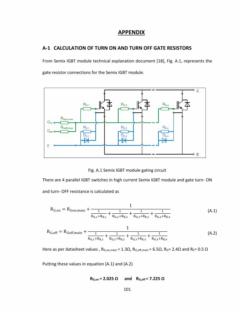
101
APPENDIX
A-1 CALCULATION OF TURN ON AND TURN OFF GATE RESISTORS
From Semix IGBT module technical explanation document [18], Fig. A.1, represents the
gate resistor connections for the Semix IGBT module.
Fig. A.1 Semix IGBT module gating circuit
There are 4 parallel IGBT switches in high current Semix IGBT module and gate turn- ON
and turn- OFF resistance is calculated as
RG,on = RGon,main +
11
RG,1+RE,1+
1
RG,2+RE,2+
1
RG,3+RE,3+
1
RG,4+RE,4
(A.1)
Here as per datasheet values , RG,on,main = 1.3Ω, RG,off,main = 6.5Ω, RG= 2.4Ω and RE= 0.5 Ω
Putting these values in equation (A.1) and (A.2)
RG,on = 2.025 Ω and RG,off = 7.225 Ω
RG,off = RGoff,main +1
1
RG,1+RE,1+
1
RG,2+RE,2+
1
RG,3+RE,3+
1
RG,4+RE,4
(A.2)

102
A-2 POWER LOSS CALCULATION
SWITCHING POWER LOSS: Manufacturer datasheet parameters are used to evaluate the
switching loss of the IGBT and the diodes [28] [29]
Switching power loss in the IGBT:
The switching power loss of the IGBT is given by
𝑃𝑠𝑤𝑖𝑡𝑐ℎ = (𝐸𝑜𝑛 + 𝐸𝑜𝑓𝑓) ∗ 𝑓𝑠𝑤 (A-3)
Where Eon = the switch turn ON energy loss
Eoff = switch turn OFF energy loss
fsw = switching frequency (switch S1)
From the plot of switching loss vs collector current, the turn on and turn off energy loss
can be found at particular collector current. To measure the losses accurately the plots
were reproduced in the Microsoft Excel and the energy loss corresponding to particular
current was measured using curve fitting feature of Microsoft excel.
Fig A.2 Shows the Eon and Eoff curves vs Ic at Tmax for the Semix604GAL12E4s IGBT
module.
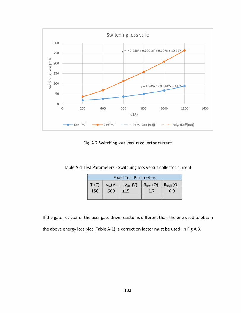
103
Fig. A.2 Switching loss versus collector current
Table A-1 Test Parameters - Switching loss versus collector current
Fixed Test Parameters
Tj (C) Vcc(V) VGE (V) RGon (Ω) RGoff (Ω)
150 600 ±15 1.7 6.9
If the gate resistor of the user gate drive resistor is different than the one used to obtain
the above energy loss plot (Table A-1), a correction factor must be used. In Fig A.3.
y = 4E-05x2 + 0.0102x + 14.3
y = -4E-08x3 + 0.0001x2 + 0.097x + 10.667
0
50
100
150
200
250
300
0 200 400 600 800 1000 1200 1400
Swit
chin
g Lo
ss (
mJ)
Ic (A)
Switching loss vs Ic
Eon (mJ) Eoff(mJ) Poly. (Eon (mJ)) Poly. (Eoff(mJ))
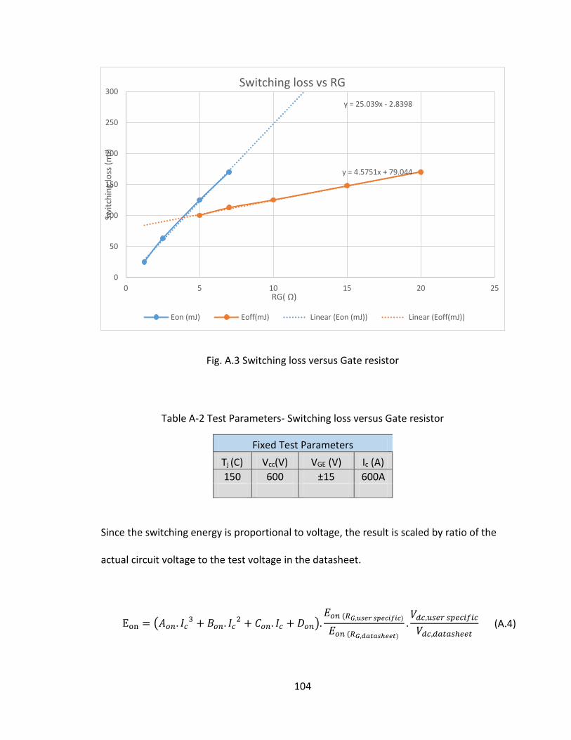
104
Fig. A.3 Switching loss versus Gate resistor
Table A-2 Test Parameters- Switching loss versus Gate resistor
Fixed Test Parameters
Tj (C) Vcc(V) VGE (V) Ic (A)
150 600 ±15 600A
Since the switching energy is proportional to voltage, the result is scaled by ratio of the
actual circuit voltage to the test voltage in the datasheet.
Eon = (𝐴𝑜𝑛. 𝐼𝑐
3 + 𝐵𝑜𝑛. 𝐼𝑐2 + 𝐶𝑜𝑛. 𝐼𝑐 + 𝐷𝑜𝑛).
𝐸𝑜𝑛 (𝑅𝐺,𝑢𝑠𝑒𝑟 𝑠𝑝𝑒𝑐𝑖𝑓𝑖𝑐)
𝐸𝑜𝑛 (𝑅𝐺,𝑑𝑎𝑡𝑎𝑠ℎ𝑒𝑒𝑡)
.𝑉𝑑𝑐,𝑢𝑠𝑒𝑟 𝑠𝑝𝑒𝑐𝑖𝑓𝑖𝑐
𝑉𝑑𝑐,𝑑𝑎𝑡𝑎𝑠ℎ𝑒𝑒𝑡 (A.4)
y = 25.039x - 2.8398
y = 4.5751x + 79.044
0
50
100
150
200
250
300
0 5 10 15 20 25
Swit
chin
g lo
ss (
mJ)
RG( Ω)
Switching loss vs RG
Eon (mJ) Eoff(mJ) Linear (Eon (mJ)) Linear (Eoff(mJ))

105
Eoff = (𝐴𝑜𝑓𝑓 . 𝐼𝑐
2 + 𝐵𝑜𝑓𝑓. 𝐼𝑐 + 𝐶𝑜𝑓𝑓).𝐸𝑜𝑓𝑓 (𝑅𝐺,𝑢𝑠𝑒𝑟 𝑠𝑝𝑒𝑐𝑖𝑓𝑖𝑐)
𝐸𝑜𝑓𝑓 (𝑅𝐺,𝑑𝑎𝑡𝑎𝑠ℎ𝑒𝑒𝑡)
.𝑉𝑑𝑐,𝑢𝑠𝑒𝑟 𝑠𝑝𝑒𝑐𝑖𝑓𝑖𝑐
𝑉𝑑𝑐,𝑑𝑎𝑡𝑎𝑠ℎ𝑒𝑒𝑡 (A.5)
Here constants A,B,C and D for turn ON and turn OFF cases are shown in Fig A.2.
Also RGon, user specific = 2.025 Ω, RGon, datasheet = 1.7 Ω, RGoff, user specific = 7.225 Ω
RGoff, datasheet = 6.9 Ω, Vdc, user specific = 500V and Vdc datasheet = 600V
For switch S1, Vdc= 500V and Ic = 200A, fsw = 5000
But in the actual waveform implementation the pulse width is 2ms followed by an off
period or zero current recording period of 15ms such that the overall current waveform
frequency is 60Hz.
So the total power loss is multiplied by the duty cycle of the current waveform which is
D =Ton
Ts=
2ms
16.67ms
Pswitch = (Eon + Eoff) ∗ fsw ∗ D (A.6)
For switch 2 the switching frequency is 60Hz. Also for switch S2, D=1.
Putting above calculated parameters for Switch S1 and Switch S2,
Pssw1 = 27.9 W and Pssw2= 2.8 W
Switching power loss in antiparallel diodes: In hard switching the diodes in antiparallel
to the IGBTs does not conduct the current at any time of the fundamental period

106
therefore there are no switching or conduction losses associated with the antiparallel
diodes.
Switching power loss in freewheeling diode:
Turn on energy of the diode is given by, 𝐸𝑜𝑛 = 1
4∗ 𝑄𝑟𝑟 ∗ 𝑈𝑑𝑟 (A.7)
Where Udr = Vdc= 500
And Qrr = Diode reverse recovery charge (from datasheet) = 100 µC
And Power loss = Pon = Eon* fsw * D = 0.0125*5000 *0.12= 7.5 W
The turn off losses in the diode are generally small and is neglected
Therefore diode switching power loss = Psfwd1 = 7.5 W
Switching loss for the 2nd freewheeling diode = Psfwd2 = 0.0125*60 = 0.75W
CONDUCTION LOSS:
Conduction loss in the IGBT: Fig A.4 represents the collector current versus collector-
emitter voltage characteristics for the Semix IGBT.
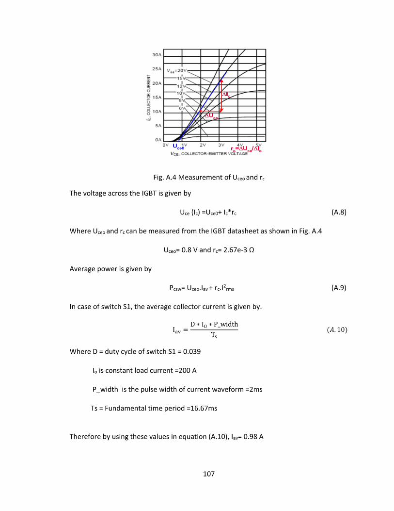
107
Fig. A.4 Measurement of Uceo and rc
The voltage across the IGBT is given by
Uce (Ic) =Uce0+ Ic*rc (A.8)
Where Uceo and rc can be measured from the IGBT datasheet as shown in Fig. A.4
Uceo= 0.8 V and rc= 2.67e-3 Ω
Average power is given by
Pcsw= Uceo.Iav + rc.I2rms (A.9)
In case of switch S1, the average collector current is given by.
Iav =D ∗ I0 ∗ P_width
Ts (𝐴. 10)
Where D = duty cycle of switch S1 = 0.039
Io is constant load current =200 A
P_width is the pulse width of current waveform =2ms
Ts = Fundamental time period =16.67ms
Therefore by using these values in equation (A.10), Iav= 0.98 A
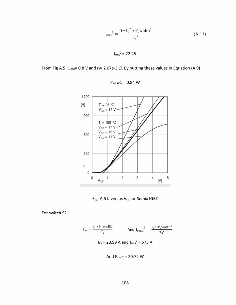
108
Irms2 =
D ∗ I02 ∗ P_width2
Ts2 (A. 11)
Irms2 = 22.45
From Fig A.5, Uceo= 0.8 V and rc= 2.67e-3 Ω. By putting these values in Equation (A.9)
Pcsw1 = 0.84 W
Fig. A.5 Ic versus Vce for Semix IGBT
For switch S2,
Iav =I0 ∗ P_width
Ts
And Irms2 =
I02∗P_width2
Ts2
Iav = 23.99 A and Irms2 = 575 A
And Pcsw2 = 20.72 W
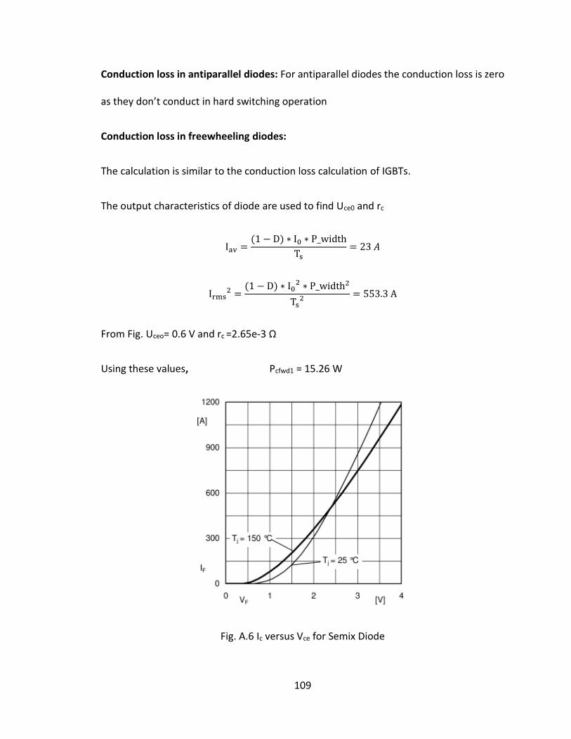
109
Conduction loss in antiparallel diodes: For antiparallel diodes the conduction loss is zero
as they don’t conduct in hard switching operation
Conduction loss in freewheeling diodes:
The calculation is similar to the conduction loss calculation of IGBTs.
The output characteristics of diode are used to find Uce0 and rc
Iav =(1 − D) ∗ I0 ∗ P_width
Ts= 23 𝐴
Irms2 =
(1 − D) ∗ I02 ∗ P_width2
Ts2 = 553.3 A
From Fig. Uceo= 0.6 V and rc =2.65e-3 Ω
Using these values, Pcfwd1 = 15.26 W
Fig. A.6 Ic versus Vce for Semix Diode
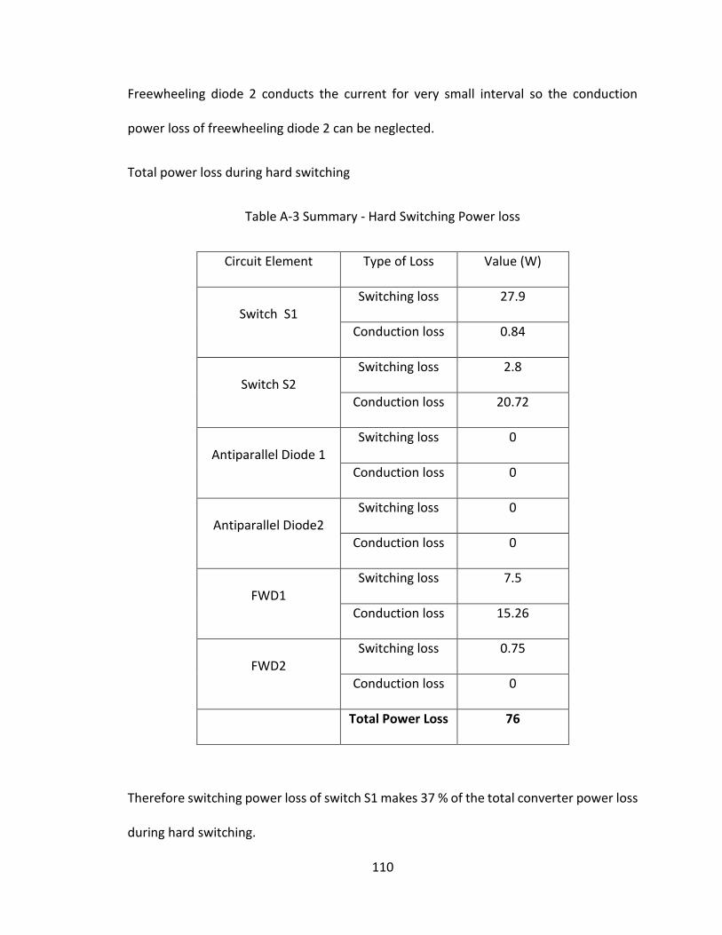
110
Freewheeling diode 2 conducts the current for very small interval so the conduction
power loss of freewheeling diode 2 can be neglected.
Total power loss during hard switching
Table A-3 Summary - Hard Switching Power loss
Circuit Element Type of Loss Value (W)
Switch S1 Switching loss 27.9
Conduction loss 0.84
Switch S2 Switching loss 2.8
Conduction loss 20.72
Antiparallel Diode 1 Switching loss 0
Conduction loss 0
Antiparallel Diode2 Switching loss 0
Conduction loss 0
FWD1 Switching loss 7.5
Conduction loss 15.26
FWD2 Switching loss 0.75
Conduction loss 0
Total Power Loss 76
Therefore switching power loss of switch S1 makes 37 % of the total converter power loss
during hard switching.