Embed Size (px)
Citation preview
A High-Voltage Temperature Compensated Logarithmic Amplifier Suitable for Integration in a
BiCMOS Power Controller IC
William C. Dillard, Jr. 200 Broun Hall
ECE Department Auburn University, AL, 36849
Abstract— A new logarithmic amplifier suitable for integration in controller IC’s for power electronics systems is introduced. The amplifier can be implemented in standard BiCMOS technologies commonly used to manufacture controller IC’s but consumes little silicon real estate as compared to commercial log amplifiers, leaving room for primary controller features. Particularly suitable to high voltage measurements at low power, the amplifier includes internal temperature compensation.
The amplifier is in fabrication using the TSMC 0.35 µm technology node. Simulations results at a single supply of 3.3 V predict true logarithmic performance with only 1.5 mW of quiescent power consumption. The active area of the amplifier (sans I/O pads) is 100 µm x 125 µm.
Keywords-logarithmic amplifier, power controller, power controller, temperature compensation.
I. INTRODUCTION Simple voltage dividers are commonly used to scale large
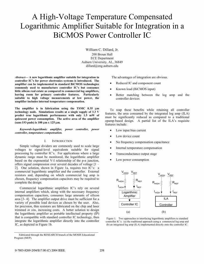
voltages to signal-level equivalents suitable for signal processing by controller IC’s. For applications where a large dynamic range must be monitored, the logarithmic amplifier based on the exponential V-I relationship of the p-n junction, offers signal compression over several decades of voltage [1 – 2]. One solution, shown in Figure 1a, requires two IC’s: a commercial logarithmic amplifier and the controller. External resistors and, depending on which commercial log amp is chosen, frequency compensation capacitors may be required to complete the design.
Commercial logarithmic amplifiers IC’s rely on several internal amplifiers which, along with the necessary frequency compensation capacitors, consumes large amounts of silicon area [3- 4]. The amplifier output drive must be sufficient for a variety of possible load devices as chosen by the user. Also, for precision, thin resistors are fabricated on the chip and laser trimmed in situ, increasing costs. A better solution to design the logarithmic amplifier as portable intellectual property (IP) that is compatible with standard controller IC technology, then integrate the logarithmic amplifier directly into the controller IC, as depicted in Figure 1b.
The advantages of integration are obvious.
• Reduced IC and component count
• Known load (BiCMOS input)
• Better matching between the log amp and the controller devices
To reap these benefits while retaining all controller features, the area consumed by the integrated log amp (ILA) must be significantly reduced as compared to a traditional opamp-based design. A partial list of the ILA’s requisite features include:
• Low input bias current
• Low device count
• No frequency compensation capacitance
• Internal temperature compensation
• Transconductance output stage
• Low power consumption
LogarithmicAmplifier
Controller IC
VHIGH VREF
RHIGH RREF
IREFIHIGH
ILA
Controller
VHIGH VREF
RHIGH RREF
IREFIHIGH
(a) (b)
Figure 1. Two approaches to interfacing logarithmic amplifiers to standard controller IC’s: (a) the traditional approach using a commercial log amp and (b) an integrated log amp (ILA) implemented directly onto the controller IC.
Fabricated through the RESEARCH branch of the MOSIS Educational Program (MEP).
0-7803-8269-2/04/$17.00 (C) 2004 IEEE. 258
II. LOGARITMIC AMPLIFIERS - THEORY OF OPERATION
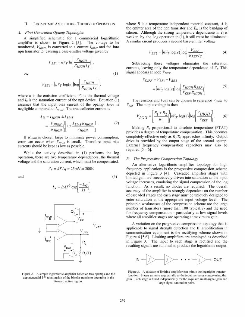
A. First Generation Opamp Topologies A simplified schematic for a commercial logarithmic
amplifier is shown in Figure 2 [3]. The voltage to be monitored, VHIGH, is converted to a current IHIGH and fed into npn transistor Q1 causing a base-emitter voltage given by
=
SHIGH
HIGHTBE IR
VnVV ln1 ,
or, (1)
[ ]
=
SHIGH
HIGHTBE IR
VenVV log)log(1 .
where n is the emission coefficient, VT is the thermal voltage and IS is the saturation current of the npn device. Equation (1) assumes that the input bias current of the opamp. IBIAS, is negligible compared to IHIGH. The true collector current is
±
=
±=
HIGH
HIGHBIAS
HIGH
HIGH
BIASHIGHD
VRI
RV
III
1 . (2)
If RHIGH is chosen large to minimize power consumption, error can occur when VHIGH is small. Therefore input bias currents should be kept as low as possible.
While the activity described in (1) performs the log operation, there are two temperature dependences, the thermal voltage and the saturation current, which must be compensated.
300Kat 25mV/ ≈= qkTVT
and (3)
−=
kTE
BATI GS exp3
IHIGH
IREF
VDIFF
R1(T)
R2
VLOG
_VBE2+
+ VBE1 -
Q1
Q2
Figure 2. A simple logarithmic amplifier based on two opamps and the exponenential I-V relationship of the bipolar transistor operating in the
forward active region.
where B is a temperature independent material constant, A is the emitter area of the npn transistor and EG is the bandgap of silicon. Although the strong temperature dependence in IS is weaken by the log operation in (1), it still must be eliminated. A similar circuit produces a second base-emitter voltage
[ ]
=
SREF
REFTBE IR
VenVV log)log(2 . (4)
Subtracting these voltages eliminates the saturation currents, leaving only the temperature dependence of VT. This signal appears at node VDIFF.
[ ]
=
−=
HIGHREF
REFHIGHT
BEBEDIFF
RVRV
enV
VVV
log)log(
21
(5)
The resistors and VREF can be chosen to reference VHIGH to VREF. The output voltage is then
[ ]
+=
REFVHIGHV
eTnVR
RRLOGV log)log(
121 . (6)
Making R1 proportional to absolute temperature (PTAT) provides a degree of temperature compensation. This becomes completely effective only as R2/R1 approaches infinity. Output drive is provided by the output stage of the second opamp. External frequency compensation capacitors may also be required [5 – 6].
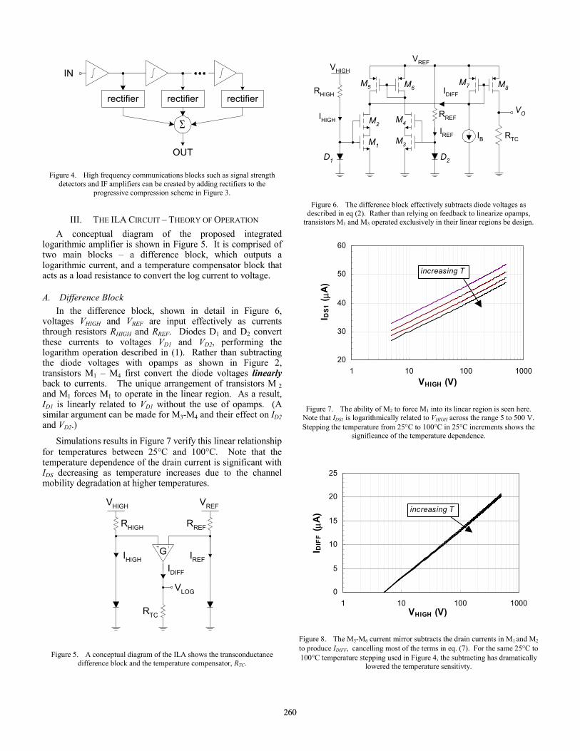
B. The Progressive Compression Topology An alternative logarithmic amplifier topology for high
frequency applications is the progressive compression scheme depicted in Figure 3 [4]. Cascaded amplifier stages with limited gain are successively driven into saturation as the input voltage increases, emulating the signal compression of the log function. As a result, no diodes are required. The overall accuracy of the amplifier is strongly dependent on the number of cascaded stages and each stage must be uniquely designed to enter saturation at the appropriate input voltage level. The principle weaknesses of the compression scheme are the large number of transistors (more than 100 typically) and the need for frequency compensation – particularly at low signal levels where all amplifier stages are operating at maximum gain.
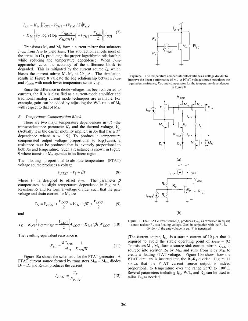
A variation on the progressive compression topology that is applicable to signal strength detection and IF amplification in communication equipment is the rectifying scheme shown in Figure 4 [5,6]. Limiting amplifiers are employed as described in Figure 3. The input to each stage is rectified and the resulting signals are summed to produce the logarithmic output.
IN OUT
Figure 3. A cascade of limiting amplifier can mimic the logarithm transfer function. Stages saturate sequentially as the input increases compressing the
gain. Each stage is tuned independently for the requisite small-signal gain and large signal saturation point.
259
IN
OUT
rectifier rectifier rectifier
Σ
Figure 4. High frequency communications blocks such as signal strength detectors and IF amplifiers can be created by adding rectifiers to the
progressive compression scheme in Figure 3.
III. THE ILA CIRCUIT – THEORY OF OPERATION A conceptual diagram of the proposed integrated
logarithmic amplifier is shown in Figure 5. It is comprised of two main blocks – a difference block, which outputs a logarithmic current, and a temperature compensator block that acts as a load resistance to convert the log current to voltage.
A. Difference Block In the difference block, shown in detail in Figure 6,
voltages VHIGH and VREF are input effectively as currents through resistors RHIGH and RREF. Diodes D1 and D2 convert these currents to voltages VD1 and VD2, performing the logarithm operation described in (1). Rather than subtracting the diode voltages with opamps as shown in Figure 2, transistors M1 – M4 first convert the diode voltages linearly back to currents. The unique arrangement of transistors M 2 and M1 forces M1 to operate in the linear region. As a result, ID1 is linearly related to VD1 without the use of opamps. (A similar argument can be made for M3-M4 and their effect on ID2 and VD2.)
Simulations results in Figure 7 verify this linear relationship for temperatures between 25°C and 100°C. Note that the temperature dependence of the drain current is significant with IDS decreasing as temperature increases due to the channel mobility degradation at higher temperatures.
VLOG
RTC
IDIFF
VHIGH VREF
RHIGH RREF
IHIGH IREFG
Figure 5. A conceptual diagram of the ILA shows the transconductance difference block and the temperature compensator, RTC.
IDIFF
VHIGH
VREF
RHIGH
RREFIHIGH
IREFM1
M2
M5 M6
M3
M4
M7 M8
RTC
VO
D1 D2
IB
Figure 6. The difference block effectively subtracts diode voltages as described in eq (2). Rather than relying on feedback to linearize opamps,
transistors M1 and M3 operated exclusively in their linear regions be design.
20
30
40
50
60
1 10 100 1000VHIGH (V)
I DS1
( µA)
increasing T
Figure 7. The ability of M2 to force M1 into its linear region is seen here. Note that IDS1 is logarithmically related to VHIGH across the range 5 to 500 V. Stepping the temperature from 25°C to 100°C in 25°C increments shows the
significance of the temperature dependence.
0
5
10
15
20
25
1 10 100 1000VHIGH (V)
I DIF
F ( µ
A) increasing T
Figure 8. The M5-M6 current mirror subtracts the drain currents in M1 and M2
to produce IDIFF, cancelling most of the terms in eq. (7). For the same 25°C to 100°C temperature stepping used in Figure 4, the subtracting has dramatically
lowered the temperature sensitivty.
260
[ ]
11
11
111111
2log)log(
)2/(
DSDS
THSHIGH
HIGHTN
DSDSTHGSND
VV
VIR
VeVK
VVVVKI
−−
≈
−−=
(7)
Transistors M5 and M6 form a current mirror that subtracts IHIGH from IREF to yield IDIFF. This subtraction cancels most of the terms in (7), producing the proper logarithmic relationship while reducing the temperature dependence. When IDIFF approaches zero, the accuracy of the difference block is degraded. This is mitigated by the current source IB, which biases the current mirror M7-M8 at 20 µA. The simulation results in Figure 8 validate the log relationship between IDIFF and VHIGH with much lower temperature sensitivity.
Since the difference in diode voltages has been converted to currents, the ILA is classified as a current-mode amplifier and traditional analog current mode techniques are available. For example, gain can be added by adjusting the W/L ratio of M8 with respect to that of M7.
B. Temperature Compensation Block There are two major temperature dependencies in (7) –the
transconductance parameter KN and the thermal voltage, VT. (Actually it is the carrier mobility implicit in KN that has a T-n dependence where n ≈ 1.5.) To produce a temperature compensated output voltage proportional to log(VHIGH), a resistance must be produced that is inversely proportional to both KN and temperature. Such a resistance is shown in Figure 9 where transistor M9 operates in its linear region.
The floating proportional-to-absolute-temperature (PTAT) voltage source produces a voltage
TVVPTAT β+= 1 (8)
where V1 is designed to offset VTH. The parameter β compensates the slight temperature dependence in Figure 8. Resistors R3 and R4 form a voltage divider such that the gate voltage and drain current for M9 are
22LOG
THLOG
PTATGV
TVV
VV ++≈+= β (9)
and
LOGNLOGLOG
THGND VTKVV
VVKI )(2 99 β≈
−−= (10)
The resulting equivalent resistance is
TKIV
RND
LOGTC β9
1∂
∂= (11)
Figure 10a shows the schematic for the PTAT generator. A PTAT current source formed by transistors M10 – M13, diodes D3 – D4 and RPTAT, produces the current
PTAT
TPTAT R
VI = (12)
IDIFF
M9VPTAT
RTC
R3
R4
Figure 9. The temperature compensator block utilizes a voltage divider to improve the linear performance of M9. A PTAT voltage source modulates the equivalent resistance, RTC, and compensates for the temperature dependences
in Figure 8.
VREF
M12
M13 M14
M10 M11
RPTAT
D3 D4
IPTAT
ISU
M15
IPTAT
RX
M16 M17
(a)
IDIFF
M9
R3
R4
VLOG
RTC
RX
IPTAT
IPTAT
(b)
Figure 10. The PTAT current source (a) produces VPTAT as expressed in eq. (8) across resistor RX as a floating voltage. Used in conjuction with the R3-R4
divider (b) the gate voltage in eq. (9) is generated.
(The current source, ISU, is a startup current of 10 µA that is required to avoid the stable operating point of IPTAT = 0.) Transistors M14-M17 form a source-sink current mirror. IPTAT is sourced into resistor RX by M14 and sunk from it by M16 to create a floating PTAT voltage. Figure 10b shows how the PTAT circuitry is inserted into the R3-R4 divider. Figure 11 shows that the PTAT current source output is indeed proportional to temperature over the range 25°C to 100°C. Several parameters including ISU, W/L, and RX can be used to tailor VG9 as needed.
261
44.0
46.0
48.0
50.0
52.0
20 40 60 80 100 120
Temperature (oC)
I PTA
T (µA
)
Figure 11. The output of the PTAT current source is very linear with temperature (0.060 µA/°C). Characteristics of IPTAT such as intercept and
slope can be controlled through the startup current source and the W/L ratios of the transistors.
Combining the two blocks, the final output voltage is generated.
=
=
HIGHREF
REFHIGH
NN
TNN
TCDIFFLOG
RVRV
TKKeVKK
RIV
log)log(
97
81β
(12)
If the external resistors are equal, the output voltage becomes
=
=
REF
HIGH
REF
HIGHLOG
VV
A
VV
qek
LWLW
LWLW
V
log
log)log()/()/(
)/()/(
7
8
9
1β
(13)
and VHIGH is normalized to VREF. (Alternatively, the external resistor ratio can be selected to normalize VHIGH to unity.) The gain, A, can be adjusted through the W/L ratios and β.
The load seen by the ILA will a BiCMOS input that requires low currents. If VLOG in (13) has enough signal swing, there is no need for a high gain output stage at all. This is a significant costs and area savings as compared to the commercial logarithmic amplifier. Since β in (13) provides temperature compensation, it is left to the W/L ratios to ensure adequate signal swing. Simulations for the entire amplifier across the two-decade input range of 5 to 500 V and the temperature range 0 to 100°C are shown in Figures 12 and 13. The percent errors are calculated against the least squares fit to the data. As expected, operating at lower voltages results in higher percent errors of 3 to 4 %. However, between 20 V and 500 V, the anticipated error is less than 1%.
C. Frequency Response Reviewing the Difference and Temperature Compensation
blocks in Figures 6 and 10, we find that there are no high impedance nodes in the entire amplifier. At each node, except the output node, the maximum impedance is only 1/gm. At the output node, the equivalent resistance is
0
0.5
1
1.5
2
2.5
3
1 10 100 1000VHIGH (V)
V LO
G (V
)
-1
0
1
2
3
4
5
Per
cent
Err
or
increasing T
Figure 12. Simulation results show the effectiveness of the temperature compensator block in canceling most temperature effects. The percent error is
calculated using a least squares fit to the data.
0.0
0.5
1.0
1.5
2.0
2.5
3.0
0 25 50 75 100 125
Temperature (oC)
VLO
G (V
)500V
50V
5V
Figure 13. Simulations for the output voltage versus temperature at three different values of VHIGH show the insensitivity to temperature across the input
voltage span.
TCoTCOUT RrRR ≈= 8// . (14)
Choosing bias currents to set RTC much less than 1/gm, the frequency response is dominated by the output capacitance – the BiCMOS input capacitance of the downstream circuitry.
As all other poles are at high frequencies, the amplifier behaves as a single pole amplifier being self-compensated by COUT and is inherently stable.
OUTOUTdB CR
fπ
=2
13 (13)
262
IV. IMPLEMENTATION The optimum technology for the ILA is a standard
BiCMOS technology. Diodes would be fabricated as diode connected bipolar transistors and a variety of diffusions would be available for resistors. As the entire ILA is analog, submicron geometries are not critical. In fact, at very small gate lengths, the channel length modulation can significantly degrade the analog performance of CMOS devices.
At present the ILA and a collection of test structures are being implemented in the TSMS 0.35 µm CMOS process through the MOSIS fabrication service [7]. Diodes are implemented in the source-drain/well diffusions. Also, well diffusions are used for integrated resistors. Upon receipt the final product, the design will be tested across the temperature range 25°C to 100°C.
REFERENCES [1] P. Gray, B Hurst, S. Lewis, R. Meyer, Analysis and Design of Analog
Integrated Circuits Fourth Edition, New York, Wiley and Sons, 2001. [2] Sedra, Smith, Microelectronics Circuits, Fifth Edition, London, Oxford
Press, 2003. [3] LOG101 datasheet, Burr Brown, May 2002. [4] K. Koli, K.Halonen, ”A 2.5 V temperature compensated CMOS
logarithmic amplifier,” Proceedings of the IEEE 1997 Custom Integrated Circuits Conference, May 1997, pp. 79 –82.
[5] B. Gilbert, B. Clarke, “Monolithic dc-to-120 MHz log-amp is stable and accurate,” Best of Analog Dialog, vol. 23, no. 3, 1989, pp. 189 – 192.
[6] K. Kimura, “A CMOS Logarithmic IF Amplifier with Unbalanced Source-Coupled Pairs,” IEEE Journal of Solid-State Circuits,, Vol. 28, no. 1, January, 1993, pp. 78 – 83.
[7] MOSIS Integrated Circuit Fabrication Service, 4676 Admiralty Way, Marina Del Rey, CA 90292-6695, URL: http://www.mosis.com/
263