Embed Size (px)
Citation preview
A High-Voltage On-Chip Power Distribution Network
by
Mustafa Munawar Shihab
A thesis submitted to the Graduate Faculty ofAuburn University
in partial fulfillment of therequirements for the Degree of
Master of Science
Auburn, AlabamaJune 28, 2013
Keywords: Low Power Design, On-Chip Power Distribution Network, System-on-ChipDesign, Interconnect Loss, Multi-core Design
Copyright 2013 by Mustafa Munawar Shihab
Approved by
Vishwani D. Agrawal,Chair, James J. Danaher Professor of Electrical and Computer Eng.Victor Nelson, Professor of Electrical and Computer Engineering
Adit D. Singh, James B. Davis Professor of Electrical and Computer Engineering
Abstract
With high performance mobile computing devices like tablets and smart-phones virtually
swiping the VLSI chip market, the industry is facing the perpetual challenge of optimizing
between power and performance, more than ever before. Although, existing Power Distribu-
tion Network (PDN) designs take into consideration issues like IR drop and crosstalk noise,
they practically ignore the actual power loss in the network. In this work we try to bridge
that gap, and propose a scheme for delivering power to different parts of a large integrated
circuit, such as modules on a System on Chip (SoC), at a higher than the regular voltage.
This increase in voltage lowers the current on the grid, and thereby reduces the I2R loss
in the on-chip power distribution network. The idea, though novel for VLSI devices, is in-
spired from the distribution system of commercial long distance power supply networks. We
propose to use on-chip DC-DC converters to downscale voltage close to the delivery points,
much like what is done in commercial power networks using transformers. This scheme can
increase the efficiency of power delivery significantly over the current designs. Theoretical
estimates, confirmed through SPICE simulations, show that when distributed at 3V (a volt-
age close to the nominal output of a Li-ion battery), and then down-converted to VDD of
1V, instead of distributing at 1V, the efficiency of the circuit can go up from a mere 60% to
more than 90%.
ii

Acknowledgments
All human achievements, trivial or momentous, are invariably indebted to contributions
from associates, peers, well-wishers and loved ones. This small work of mine is no exception,
and I am eternally grateful to all those who helped to make it possible.
Firstly, I express my sincere gratitude to my advisor Dr. Vishwani Agrawal. He has
supported and helped me from my first day at Auburn University till this point. Being a
fantastic mentor, he has always shown me the right direction, pushed me towards the goal,
and made this thesis possible. Secondly, I am grateful Dr. Adit Singh for being a member of
my thesis committee and for the two amazing courses I had the opportunity of taking with
him. I also thank Dr. Victor Nelson for agreeing to be in my committee, and for the really
helpful study-aids he has put on his website for the students.
I thank Mr. Charles Ellis from the AMSTC fabrication laboratory, for helping me out
at a really difficult time by funding me with assistantship in the lab. I am also thankful to
Dr. Suraj Sindia for his friendship and support. He has helped me greatly all through this
work, and kept the long hours in the office interesting.
I am grateful to Muhammad Asaduzzaman Shanto for being the elder brother and
looking after me all the time. He has presented me with a second home in this far-off foreign
land.
I am indebted to Farah Naz Taher for her presence in my life. She is my sister, my best
friend, and much more than that. Without her support, inspiration, and instigation this
thesis would not have materialized. In fact, for all my achievements , credit goes to her and
to the rest of my family back home.
iii

I am forever grateful to my mother, my father, and my younger brother for the sacrifice
they are incurring to make my dream come true. Without their love and unwavering support
I would not be here today.
Finally, I thank the Almighty for my life, and for adorning it with all these wonderful
people.
I dedicate this work to all those who have blessed me with selfless, unconditional love.
iv
Table of Contents
Abstract . . . . . . . . . . . . . . . . . . . . . . . . . . . . . . . . . . . . . . . . . . . ii
Acknowledgments . . . . . . . . . . . . . . . . . . . . . . . . . . . . . . . . . . . . . . iii
List of Figures . . . . . . . . . . . . . . . . . . . . . . . . . . . . . . . . . . . . . . . viii
List of Tables . . . . . . . . . . . . . . . . . . . . . . . . . . . . . . . . . . . . . . . . xi
1 Introduction . . . . . . . . . . . . . . . . . . . . . . . . . . . . . . . . . . . . . . 1
1.1 Motivation . . . . . . . . . . . . . . . . . . . . . . . . . . . . . . . . . . . . . 2
1.2 Problem Statement . . . . . . . . . . . . . . . . . . . . . . . . . . . . . . . . 5
1.3 Contribution . . . . . . . . . . . . . . . . . . . . . . . . . . . . . . . . . . . . 5
1.4 Thesis Organization . . . . . . . . . . . . . . . . . . . . . . . . . . . . . . . . 6
2 Power in Integrated Circuits . . . . . . . . . . . . . . . . . . . . . . . . . . . . . 8
2.1 Power Consumption . . . . . . . . . . . . . . . . . . . . . . . . . . . . . . . 8
2.1.1 Dynamic Power . . . . . . . . . . . . . . . . . . . . . . . . . . . . . . 9
2.1.2 Static Power . . . . . . . . . . . . . . . . . . . . . . . . . . . . . . . . 11
2.2 Methods for Power Reduction/Management . . . . . . . . . . . . . . . . . . 13
2.2.1 Reduction of Dynamic Power . . . . . . . . . . . . . . . . . . . . . . 14
2.2.2 Reduction of Static/Leakage Power . . . . . . . . . . . . . . . . . . . 18
3 Present Day On-Chip Power Distribution Network . . . . . . . . . . . . . . . . . 22
3.1 Structure of the On-Chip Distribution Network . . . . . . . . . . . . . . . . 24
3.1.1 Power Distribution Network Model . . . . . . . . . . . . . . . . . . . 25
3.2 Issues with the Current Distribution Network . . . . . . . . . . . . . . . . . 27
3.2.1 IR Drops . . . . . . . . . . . . . . . . . . . . . . . . . . . . . . . . . 28
3.2.2 LdIdt
Noise . . . . . . . . . . . . . . . . . . . . . . . . . . . . . . . . . 28
3.2.3 Electromigration in Power Interconnects . . . . . . . . . . . . . . . . 29
v
3.2.4 Signal Delay Uncertainty . . . . . . . . . . . . . . . . . . . . . . . . . 30
3.2.5 On-chip Clock Jitter . . . . . . . . . . . . . . . . . . . . . . . . . . . 30
3.2.6 Noise Margin Degradation . . . . . . . . . . . . . . . . . . . . . . . . 31
3.3 Prior Work on Improving the Network . . . . . . . . . . . . . . . . . . . . . 31
3.3.1 Wire Sizing . . . . . . . . . . . . . . . . . . . . . . . . . . . . . . . . 31
3.3.2 De-coupling Capacitances . . . . . . . . . . . . . . . . . . . . . . . . 32
3.4 I2R Power Loss across the Distribution Network . . . . . . . . . . . . . . . . 33
4 High-Voltage On-Chip Power Distribution Network . . . . . . . . . . . . . . . . 36
4.1 Inspiration: Joules Law and Long-Distance Power Transmission Grid . . . . 36
4.2 DC-DC Voltage Converters . . . . . . . . . . . . . . . . . . . . . . . . . . . . 38
4.2.1 Definition . . . . . . . . . . . . . . . . . . . . . . . . . . . . . . . . . 38
4.2.2 Types of Operation . . . . . . . . . . . . . . . . . . . . . . . . . . . . 39
4.2.3 Classification of DC-DC Converter Designs . . . . . . . . . . . . . . . 39
4.3 Construction of the Proposed Network . . . . . . . . . . . . . . . . . . . . . 43
4.4 Selection of the Distribution Voltage . . . . . . . . . . . . . . . . . . . . . . 45
4.5 Advantages of the Scheme . . . . . . . . . . . . . . . . . . . . . . . . . . . . 46
5 Experimental Setup and Results . . . . . . . . . . . . . . . . . . . . . . . . . . . 48
5.1 LTC3411-A: Step-down DC-DC Converter from Linear Technology . . . . . . 48
5.1.1 Linear Technology . . . . . . . . . . . . . . . . . . . . . . . . . . . . 48
5.1.2 LTC3411-A: Step-Down DC-DC Converter . . . . . . . . . . . . . . . 48
5.2 Experimental Setup . . . . . . . . . . . . . . . . . . . . . . . . . . . . . . . 49
5.2.1 Present Day On-chip Power Distribution Network . . . . . . . . . . . 50
5.2.2 High-Voltage On-chip Power Distribution Network Considering Ideal
DC-DC Converters . . . . . . . . . . . . . . . . . . . . . . . . . . . . 50
5.2.3 High-Voltage On-chip Power Distribution Network With Non-Ideal
DC-DC Converters . . . . . . . . . . . . . . . . . . . . . . . . . . . . 51
5.3 Results and Analysis . . . . . . . . . . . . . . . . . . . . . . . . . . . . . . . 52
vi
5.3.1 Present Day On-chip Power Distribution Network . . . . . . . . . . . 52
5.3.2 High-Voltage On-Chip Power Distribution Network Considering Ideal
DC-DC Converters . . . . . . . . . . . . . . . . . . . . . . . . . . . . 53
5.3.3 High-Voltage On-Chip Power Distribution Network Considering Non-
Ideal DC-DC Converters . . . . . . . . . . . . . . . . . . . . . . . . . 54
5.4 Discussion . . . . . . . . . . . . . . . . . . . . . . . . . . . . . . . . . . . . . 56
6 Challenges, Developments and Future Work . . . . . . . . . . . . . . . . . . . . 60
6.1 Challenges . . . . . . . . . . . . . . . . . . . . . . . . . . . . . . . . . . . . . 60
6.2 Recent Developments . . . . . . . . . . . . . . . . . . . . . . . . . . . . . . . 61
6.3 Future Work . . . . . . . . . . . . . . . . . . . . . . . . . . . . . . . . . . . . 61
7 Conclusion . . . . . . . . . . . . . . . . . . . . . . . . . . . . . . . . . . . . . . . 63
Bibliography . . . . . . . . . . . . . . . . . . . . . . . . . . . . . . . . . . . . . . . . 65
vii
List of Figures
1.1 Transistor-IC revolution [9]. . . . . . . . . . . . . . . . . . . . . . . . . . . . . . 2
1.2 Original sketched graph by Gordon Moore in 1965 [26]. . . . . . . . . . . . . . . 3
1.3 Timeline chart showing industry implementation of Moore’s Law [9]. . . . . . . 4
2.1 Dynamic power due to switching capacitances. . . . . . . . . . . . . . . . . . . . 10
2.2 Short-circuit or crowbar current. . . . . . . . . . . . . . . . . . . . . . . . . . . 10
2.3 Clock gating. . . . . . . . . . . . . . . . . . . . . . . . . . . . . . . . . . . . . . 15
2.4 Gate-level logic optimization. . . . . . . . . . . . . . . . . . . . . . . . . . . . . 16
2.5 Leakage vs. delay for a 90nm library. . . . . . . . . . . . . . . . . . . . . . . . . 18
2.6 Basic power gating circuit. . . . . . . . . . . . . . . . . . . . . . . . . . . . . . . 19
2.7 Power consumption in a system without (left) and with (right) basic power gating. 20
3.1 Time-dependent power consumption of microprocessor [46]. . . . . . . . . . . . 23
3.2 Power distribution for standard cell layout [46]. . . . . . . . . . . . . . . . . . . 24
3.3 Lumped model of power distribution system [46]. . . . . . . . . . . . . . . . . . 25
3.4 On-chip power grid [46]. . . . . . . . . . . . . . . . . . . . . . . . . . . . . . . . 26
3.5 Schematic of power grid in CMOS designs [41]. . . . . . . . . . . . . . . . . . . 27
viii
3.6 Power delivery system [46]. . . . . . . . . . . . . . . . . . . . . . . . . . . . . . 28
3.7 Power supply droop due to IR drop [46]. . . . . . . . . . . . . . . . . . . . . . . 29
3.8 Circuit model for de-coupling capacitance [42]. . . . . . . . . . . . . . . . . . . . 32
3.9 Ball Grid Array (BGA) packaging [2]. . . . . . . . . . . . . . . . . . . . . . . . 34
3.10 Land Grid Array (LGA) packaging [10]. . . . . . . . . . . . . . . . . . . . . . . 34
4.1 A typical long-distance power distribution network [5]. . . . . . . . . . . . . . . 37
4.2 A simple voltage divider circuit describing the operating principle of a linear
DC-DC converter. . . . . . . . . . . . . . . . . . . . . . . . . . . . . . . . . . . 40
4.3 Schematic representation of a switched-capacitor DC-DC converter (VDD2 = 2×
VDD1). . . . . . . . . . . . . . . . . . . . . . . . . . . . . . . . . . . . . . . . . . 41
4.4 A Comparison of different DC-DC converters [23]. . . . . . . . . . . . . . . . . . 43
4.5 A system-on-chip (SoC) with regular power distribution network. . . . . . . . . 43
4.6 A system-on-chip (SoC) with high-voltage power distribution network. . . . . . 45
5.1 Regular power distribution network (distribution voltage = 1V) for 9 loads. . . 51
5.2 High-voltage power distribution network (distribution voltage = 3V) for 9 loads. 52
5.3 Grid power consumption in the regular PDN (distribution voltage = 1V). . . . . 53
5.4 Efficiency of the regular PDN (distribution voltage = 1V). . . . . . . . . . . . . 54
5.5 Grid power consumption in the high-voltage PDN (distribution voltage = 3V)
with ideal converter. . . . . . . . . . . . . . . . . . . . . . . . . . . . . . . . . . 55
ix
5.6 Efficiency of the high-voltage PDN (distribution voltage = 3V) with ideal converter. 55
5.7 Grid power consumption in the high-voltage PDN (distribution voltage = 3V)
with non-ideal converter. . . . . . . . . . . . . . . . . . . . . . . . . . . . . . . . 56
5.8 Efficiency of the high-voltage PDN (distribution voltage = 3V) with non-ideal
converter. . . . . . . . . . . . . . . . . . . . . . . . . . . . . . . . . . . . . . . . 57
5.9 Comparison of grid power loss. . . . . . . . . . . . . . . . . . . . . . . . . . . . 58
5.10 Comparison of efficiency. . . . . . . . . . . . . . . . . . . . . . . . . . . . . . . . 59
5.11 Effect of distribution voltage on grid efficiency for a 256 load grid. . . . . . . . . 59
x

List of Tables
5.1 Power consumption break down and efficiency of the regular PDN (distributionvoltage = 1V). . . . . . . . . . . . . . . . . . . . . . . . . . . . . . . . . . . . . 53
5.2 Power consumption break down and efficiency of the high-voltage PDN (distri-bution voltage = 3V) with ideal converter. . . . . . . . . . . . . . . . . . . . . . 54
5.3 Power consumption break down and efficiency of the high-voltage PDN (distri-bution voltage = 3V) with non-ideal converter. . . . . . . . . . . . . . . . . . . 56
5.4 Comparison of grid power loss. . . . . . . . . . . . . . . . . . . . . . . . . . . . 57
5.5 Comparison of efficiency. . . . . . . . . . . . . . . . . . . . . . . . . . . . . . . . 58
xi
Chapter 1
Introduction
Since the invention of Integrated Circuits (IC) in 1959 [8], its design and architectural
development bifurcated into two distinctly different paths. For the first group, enhancing
performance was synonymous to higher clock speed, and that has been at the core of their
design process. This class of high-performance ICs has increased clock frequency many
fold over the years, using power-hungry circuit techniques and microarchitectures, and at
the cost of increased power consumption. However, this boundless power consumption has
finally become too expensive to continue with. The other group of ICs has emerged as
a result of customer demand for miniaturization and portability. Portable devices, until
recently, represented the low end of the performance spectrum with power constraints always
dominating over speed. Extended battery life and reduced system cost constraints drove the
design process. However, strong demand has been growing for higher performance in portable
equipment. Today, people expect from their tablets almost the same computing capability
as a desktop system.
Now, traditional circuits and architectures in high performance ICs, because of the
power hungry nature of these technologies, are not applicable to ICs designed for portable
systems. Alternatively, circuits and architectures that have been developed for portable de-
vices, because of the typical low throughput characteristics of these technologies, are not
effective in high performance ICs. Therefore, today the IC industry is experiencing a con-
tradiction, a shift in requirements at both the high performance and portability ends of the
market. Power dissipation is no longer a secondary issue in high performance ICs. Simi-
larly, enhancing throughput is as important as lowering the power, area, and weight in many
1

Figure 1.1: Transistor-IC revolution [9].
portable devices. The generation, distribution, and dissipation of power are now at the fore-
front of current problems faced by IC designers. A dichotomy exists in the design of modern
microelectronic systems: they must be simultaneously low power and high performance [37].
1.1 Motivation
The history of semiconductor industry dates back to 1833, when Michael Faraday discov-
ered that electrical conduction in silver sulfide crystals increases with temperature, opposite
to that observed in copper and other metals [3]. However, the industry really got into motion
in 1947, when by the team of William Shockley, John Bardeen and Walter Brattain at Bell
Laboratories invented the transistor [11]. Later, in 1959 Robert Noyce of Fairchild Semicon-
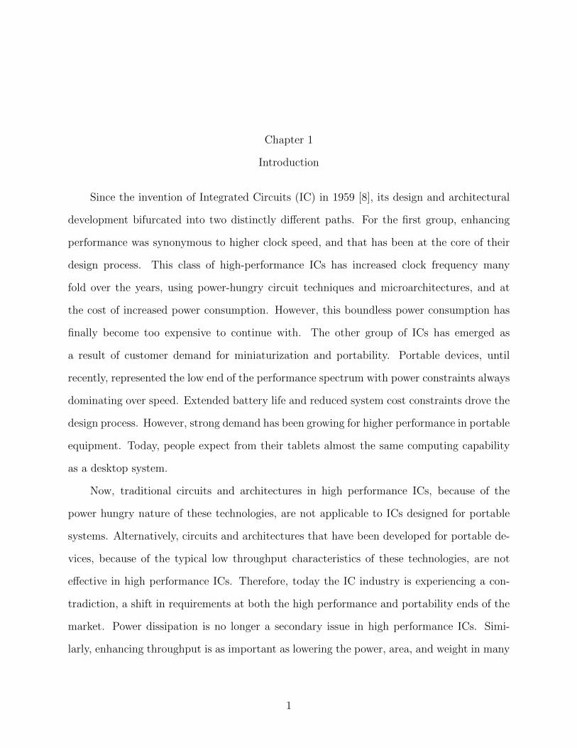
ductor invented Integrated Circuits (IC) [8] . Since then, capturing the true capability of
transistors, ICs revolutionized the silicon industry (Figure 1.1).
Over the years, both the performance and the complexity of integrated circuits have
increased dramatically. In 1965, Intel co-founder Gordon Moore observed and formulized that
- transistor density is doubling every 18 months (Figure 1.2) [26]. In 1970, this phenomenon
became famous as Moore’s Law, and has driven technology innovation across the industry
since then(Figure 1.3) [27, 28].
However, the industry is now at a critical junction where it appears that an unprece-
dented number of challenges threaten the continuation of Moore’s Law. According to [37]
the three most formidable challenges are:
2

Figure 1.2: Original sketched graph by Gordon Moore in 1965 [26].
• Technology Challenge: Carrying out the lithography process for technologies of 50nm
and beyond.
• Power Challenge: Sub-microwatt power dissipation per MIPS concurrently with thou-
sands of MIPS performance.
• Design productivity challenge: Improvement in design productivity at a rate of 50%
or higher per year.
These challenges needs to be solved in order to be able to continue the historical trends
dictated by Moore’s Law, at least for another couple of decades.
This is not a new scenario though. Design of chips has undergone a series of revolutions
all along its history. Each of these revolutions has been a response to the challenges posed
by evolving semiconductor technology. In the 1980s, the exponential increase in chip density
drove the adoption of language-based design and synthesis, providing a dramatic increase
in designer productivity. Again in the 1990s, with the beginning of million gate designs,
designers realized that there was a limit to how much new RTL could be written for a new
chip project. As a result, IP and design reuse became accepted as the only practical way to
design large chips with relatively small design teams. In the last few years, design for low
3
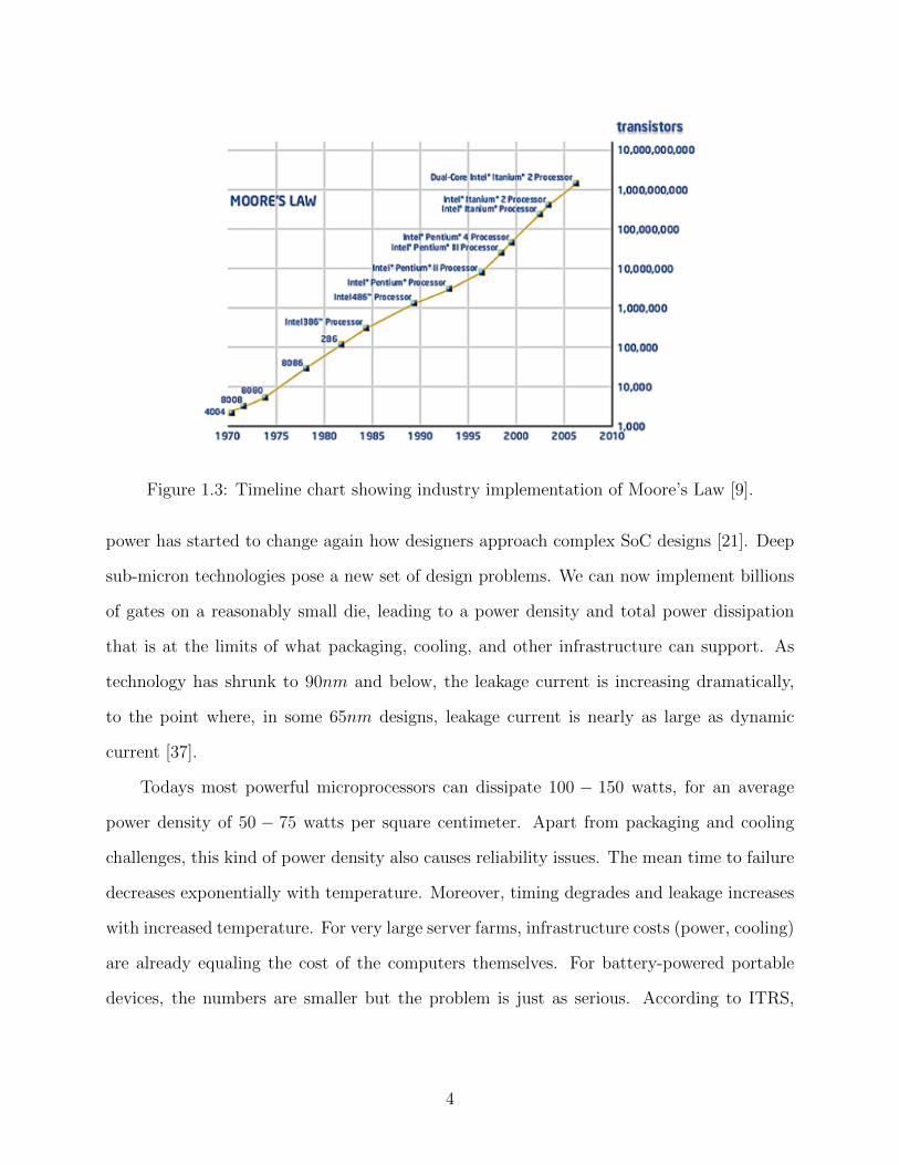
Figure 1.3: Timeline chart showing industry implementation of Moore’s Law [9].
power has started to change again how designers approach complex SoC designs [21]. Deep
sub-micron technologies pose a new set of design problems. We can now implement billions
of gates on a reasonably small die, leading to a power density and total power dissipation
that is at the limits of what packaging, cooling, and other infrastructure can support. As
technology has shrunk to 90nm and below, the leakage current is increasing dramatically,
to the point where, in some 65nm designs, leakage current is nearly as large as dynamic
current [37].
Todays most powerful microprocessors can dissipate 100 − 150 watts, for an average
power density of 50 − 75 watts per square centimeter. Apart from packaging and cooling
challenges, this kind of power density also causes reliability issues. The mean time to failure
decreases exponentially with temperature. Moreover, timing degrades and leakage increases
with increased temperature. For very large server farms, infrastructure costs (power, cooling)
are already equaling the cost of the computers themselves. For battery-powered portable
devices, the numbers are smaller but the problem is just as serious. According to ITRS,
4

battery life for these devices peaked in 2004. Since then battery life has actually declined,
as features have been added faster than power (per feature) has been reduced [21].
These changes are having a paramount effect on IC design. Designers are using ag-
gressive approaches at every step of the design process, from software to architecture to
implementation. Designers are designing multi-processor chips instead of chips with a sin-
gle, ultra-high speed processor. Through power gating, blocks in a chip are powered down
when not in use. Multi-threshold libraries are being used that can trade off leakage current
for speed. Designers are moving from a monolithic approach of powering the whole chip
with a single supply voltage to multiple supply architectures. Different blocks are running at
different voltages, depending on their individual requirements. In some cases, designers are
using scaling techniques to change the supply voltage and clock frequency to critical blocks
depending on their workload and required performance.
However, though all these researches are being carried out to find power reduction
techniques for different levels of design abstraction, the power distribution network for the
chips is mostly left out in this endeavor. The prospect of potential power savings in the
power distribution network itself is not getting enough consideration.
1.2 Problem Statement
In this thesis we propose a scheme for delivering power to different parts of a large
integrated circuit, such as modules on a System on Chip (SoC), at a higher than the regular
voltage. This increase in voltage lowers the current on the grid, and thereby reduces the I2R
loss in the on-chip power distribution network.
1.3 Contribution
While extensive research is being carried out to find power reduction techniques for
different levels of design abstraction, the prospect of potential power savings in the power
distribution network itself seems to lack attention.
5
We know that power loss in a resistive conductor is: P = I2R, where R is the resistance
of the wire. In our proposed solution, we will deliver power to different parts of a large
integrated circuit, at a higher than regular voltage (i.e., lower current) to reduce this I2R
loss in the on-chip power distribution network.
Our idea is inspired from the widely used power distribution scheme in commercial and
home networks, where power is transported from source to destination via transmission lines
that carry small currents, albeit at high voltages, consequently saving enormous amounts of
power that would have otherwise amounted to heating losses in the long distance wires.
We have simulated the regular power distribution network and our proposed high-voltage
network for 4, 9, 16, 25, 64, 100 and 256 loads. We have analyzed the results and compared
the power consumed by the network designs. We have efficiency improvement of 20− 30%,
and the trend clearly points out that it will only increase with even larger networks.
Therefore, we expect that this scheme will eventually contribute in increasing the effi-
ciency of power delivery significantly over the technique currently in use.
1.4 Thesis Organization
The rest of this thesis is broadly divided into six chapters. The organization of the
chapters is as follows:
Chapter 2 is the background review of the thesis. It contains discussion on power
consumption in CMOS circuits and methods applied to minimize and manage them.
Chapter 3 discusses present day on-chip power distribution networks (PDN). It talks
about problems with the present day network, and present and prior works and methods to
improve it. It also introduces the issue of I2R power loss in the network.
Chapter 4 introduces the proposed high-voltage on-chip power distribution network and
what inspired the idea. It discusses DC-DC converters. It also describes the construction of
the high-voltage PDN and its probable advantages.
6

Chapter 5 contains a description of the experimental setup for our scheme, the results
and a discussion on them.
Chapter 6 discusses the challenges in implementing the concept and some recent devel-
opments in overcoming those challenges. It also discusses future works to be done to take
the idea further ahead.
Chapter 7 finally summarizes and concludes the thesis.
7

Chapter 2
Power in Integrated Circuits
Traditionally, power was only a secondary concern for integrated circuit designers. Until
recently, analysis and management of power consumption was considered only after timing,
area and cost requirements were met [21, 23]. However, the situation has completely changed
now. Power is one of the first and most important design criteria today. Deep sub-micron
technologies now enable us to implement billions of gates on a small die, but that leads
power density and total power dissipation to the limits of what packaging, cooling, and
other structures can support. Apart from packaging and cooling challenges, this kind of
power density also causes reliability issues. The mean time to failure decreases exponentially
as temperature increases. Moreover, timing degrades and leakage increases with increased
temperature. Therefore, today every design has a pre-allocated power budget, which must
not be exceeded for the successful implementation of a chip [21].
This chapter contains a holistic discussion on the aspects of power in modern day in-
tegrated circuits. In the first section, power consumption in integrated circuits has been
broken down to its components and explained. The second section talks about the measures
that are taken in the industry to reduce and manage power consumption.
2.1 Power Consumption
Power consumption in modern day CMOS circuit has two main components:
• Dynamic Power
• Static Power
8
All of the power consumed in a chip can be attributed to these two broad categories [16, 21,
46, 39]. In other words,
PTotal = PDynamic + PStatic (2.1)
Where,
PTotal = Total Power Consumed by the circuit
PDynamic = Dynamic power consumed by the circuit due to switching of load capacitance
and short-circuit current between VDD and Ground
PStatic = Static power dissipated due to various leakage currents
2.1.1 Dynamic Power
Dynamic power is defined as the power consumed when the device is in active state. It
has been the dominant source of the power dissipation in VLSI circuits [37]. Dynamic power
again has two components: dynamic dissipation due to switching capacitances (PSwitching)
and dynamic dissipation due to short-circuit current (PShort−Circuit) [23]. So, dynamic power
can be written as:
PDynamic = PSwitching + PShort−circuit (2.2)
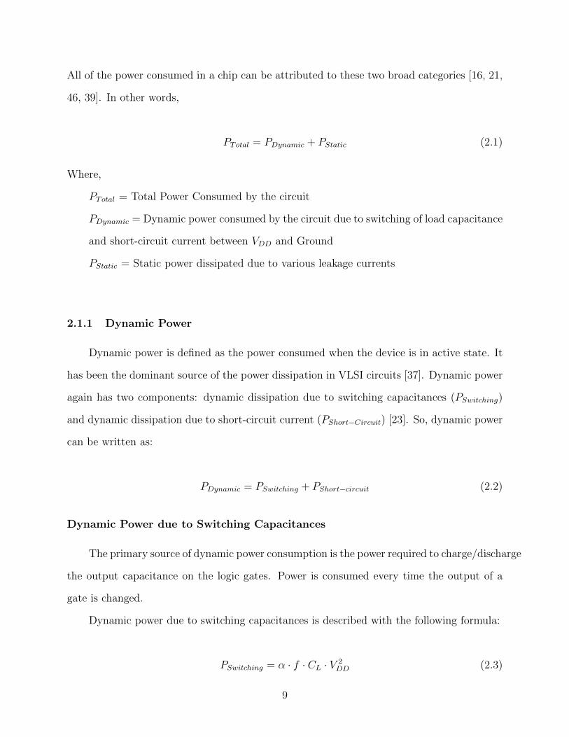
Dynamic Power due to Switching Capacitances
The primary source of dynamic power consumption is the power required to charge/discharge
the output capacitance on the logic gates. Power is consumed every time the output of a
gate is changed.
Dynamic power due to switching capacitances is described with the following formula:
PSwitching = α · f · CL · V 2DD (2.3)
9
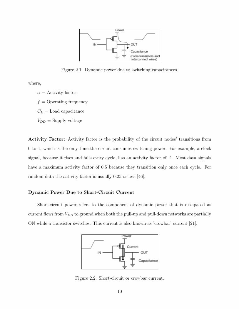
Figure 2.1: Dynamic power due to switching capacitances.
where,
α = Activity factor
f = Operating frequency
CL = Load capacitance
VDD = Supply voltage
Activity Factor: Activity factor is the probability of the circuit nodes’ transitions from
0 to 1, which is the only time the circuit consumes switching power. For example, a clock
signal, because it rises and falls every cycle, has an activity factor of 1. Most data signals
have a maximum activity factor of 0.5 because they transition only once each cycle. For
random data the activity factor is usually 0.25 or less [46].
Dynamic Power Due to Short-Circuit Current
Short-circuit power refers to the component of dynamic power that is dissipated as
current flows from VDD to ground when both the pull-up and pull-down networks are partially
ON while a transistor switches. This current is also known as ’crowbar’ current [21].
Figure 2.2: Short-circuit or crowbar current.
10
Short-circuit power dissipation increases as the input edge rates become slower because
both networks are ON for more time. On the other hand, it decreases as load capacitance
increases because with large loads the output only switches a small amount during the input
transition. Short-circuit power is strongly sensitive to the ratio v = Vt/VDD. In the limit
that v > 0.5, short-circuit current is eliminated entirely because the pull-up and pull-down
networks are never simultaneously ON. In nanometer processes, Vt can scarcely fall below
0.3V without excessive leakage, and VDD is on the order of 1V, so short-circuit current has
become almost negligible [36, 37].
2.1.2 Static Power
Static power is the power consumed when the device is powered up but no signals are
changing value. In CMOS devices, static power consumption is due to leakage currents [16,
21]. There are four major sources of leakage currents in a CMOS gate:
Sub-threshold Leakage (ISub)
The sub-threshold current is the drain-source current of an OFF transistor [36]. This
is the current that flows from the drain to the source of a transistor operating in the weak
inversion mode. Sub-threshold leakage occurs when a CMOS gate is not turned completely
off. A decent approximation of this current can be given by:
ISUB = µCoxV2th
W
Le
VGS−VTnVth (2.4)
where,
W, L = Dimensions of the transistor
Vth = Thermal voltage
n = A function of the device fabrication process which ranges from 1.0 to 2.5
11
This equation tells us that sub-threshold leakage depends exponentially on the differ-
ence between VGS and VT . Therefore, as we scale VDD and VT down for reducing dynamic
power, we make leakage power exponentially worse. In fact decreasing the threshold voltage
by 100 mv increases the leakage current by a factor of 10 [21].
Decreasing the length of transistors increases the leakage current as well. Therefore, in
a chip, transistors that have smaller threshold voltage and/or length due to process variation
contribute more to the overall leakage.
Sub-threshold leakage current increases exponentially with temperature. This greatly
complicates the problem of designing low power systems. Even if the leakage at room tem-
perature is acceptable, at worst case temperature it can exceed the design goals of the chip.
Gate Leakage (IGate)
Gate leakage current flows directly from the gate through the oxide to the substrate
due to gate oxide tunneling and hot carrier injection. Gate leakage occurs as a result of
tunneling current through the gate oxide. The gate oxide thickness (Tox) is only a few atoms
thick now - this is so thin that tunneling current can become substantial. Its magnitude
increases exponentially with the gate oxide thickness Tox and supply voltage VDD. In fact,
every 0.2nm reduction in Tox causes a tenfold increase in IGATE [37]. In previous technology
nodes, leakage current was dominated by sub-threshold leakage. But starting with 90nm,
gate leakage has been nearly 1/3 as much as sub-threshold leakage. In 65nm it was predicated
to equal sub-threshold leakage in some cases. However, presently high-k dielectric materials
are used to keep gate leakage in check. This appears to be the only effective way of reducing
gate leakage [31].
Reverse Bias Junction Leakage (IRev)
Reverse bias junction leakage occurs from the source or drain to the substrate through
the reverse-biased diodes when a transistor is OFF [21]. It is caused by minority carrier drift
12
and generation of electron/hole pairs in the depletion regions. For instance, in the case of
an inverter with low input voltage, the nMOS is OFF, the pMOS is ON, and the output
voltage is high. Subsequently, the drain-to-substrate voltage of the OFF nMOS transistor is
equal to the supply voltage. This results in a leakage current from the drain to the substrate
through the reverse-biased diode. The magnitude of the diode leakage current depends on
the area of the drain diffusion and the leakage current density, which is in turn determined
by the process technology [36].
Gate Induced Drain Leakage (IGIDL)
Gate induced drain leakage is the current which flows from the drain to the substrate
induced by a high field effect in the MOSFET drain caused by a high drain to gate voltage
(VDG) [16, 36].
2.2 Methods for Power Reduction/Management
Power consumption is one of the primary concerns for today’s circuit designers. The
generation, distribution, and dissipation of power are now at the forefront of current problems
faced by IC designers. Failure to meet the power budget for a chip exposes it to failure
from packaging and cooling challenges, reliability issues, timing degradation and increased
leakage. As discussed in the earlier section, total power consumption in CMOS is divided
into dynamic power and static/leakage power. To make a system power efficient, both need
to be minimized. However, there is an inherent contradiction in reducing dynamic and static
power. We reduce supply voltage to reduce dynamic power from switching load capacitances,
but this diminishes performance of the chip. In order to maintain performance, along with
supply voltage we need scale down threshold voltage as well. However, this reduction in
turn increases leakage or static power [8]. In the industry, numerous strategies, methods and
measures are taken to deal with this situation. Following is a categorized discussion of these
methods taken for power management at different levels of the design process.
13
2.2.1 Reduction of Dynamic Power
The primary component of dynamic power is power dissipated through switching ca-
pacitances, and it is described as:
PSwitching = α · f · CL · V 2DD (2.5)
All the parameters - activity factor , frequency f , load capacitance C and supply voltage
V are manipulated by the designers to save on dynamic power [21]. Switching power is
linearly proportional to activity factor (data dependent), frequency and load capacitance.
So, reducing those parameters reduce dynamic power linearly. But, the supply voltage has
the greatest effect on switching power, as reducing it reduces switching power quadratically.
However, reducing supply voltage also reduces performance by slowing down the gates.
Clock Gating
Clock gating is a popular approach for lowering dynamic power [22]. The distribution
network of the clocks are responsible for a significant fraction of the dynamic power in a
chip. In fact up to 50% of the dynamic power can be spent by the clocks, as they have
the highest toggle rate in the system. Now, driving the frequency to zero drives the power
consumed to zero. In the clock gating method power consumption is reduced by turning
off clocks when they are not required Modern design tools support automatic clock gating.
They can identify circuits where clock gating can be inserted without changing the function
of the logic [16, 21, 36].
Gate-Level Power Optimization
There are a number of logic optimizations that the tools can perform to minimize
dynamic power [37]. Figure 2.4 shows two examples of possible optimizations. At the upper
part of the figure, an AND gate output has a particularly high activity. But as it is followed
14
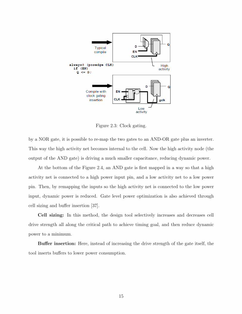
Figure 2.3: Clock gating.
by a NOR gate, it is possible to re-map the two gates to an AND-OR gate plus an inverter.
This way the high activity net becomes internal to the cell. Now the high activity node (the
output of the AND gate) is driving a much smaller capacitance, reducing dynamic power.
At the bottom of the Figure 2.4, an AND gate is first mapped in a way so that a high
activity net is connected to a high power input pin, and a low activity net to a low power
pin. Then, by remapping the inputs so the high activity net is connected to the low power
input, dynamic power is reduced. Gate level power optimization is also achieved through
cell sizing and buffer insertion [37].
Cell sizing: In this method, the design tool selectively increases and decreases cell
drive strength all along the critical path to achieve timing goal, and then reduce dynamic
power to a minimum.
Buffer insertion: Here, instead of increasing the drive strength of the gate itself, the
tool inserts buffers to lower power consumption.
15
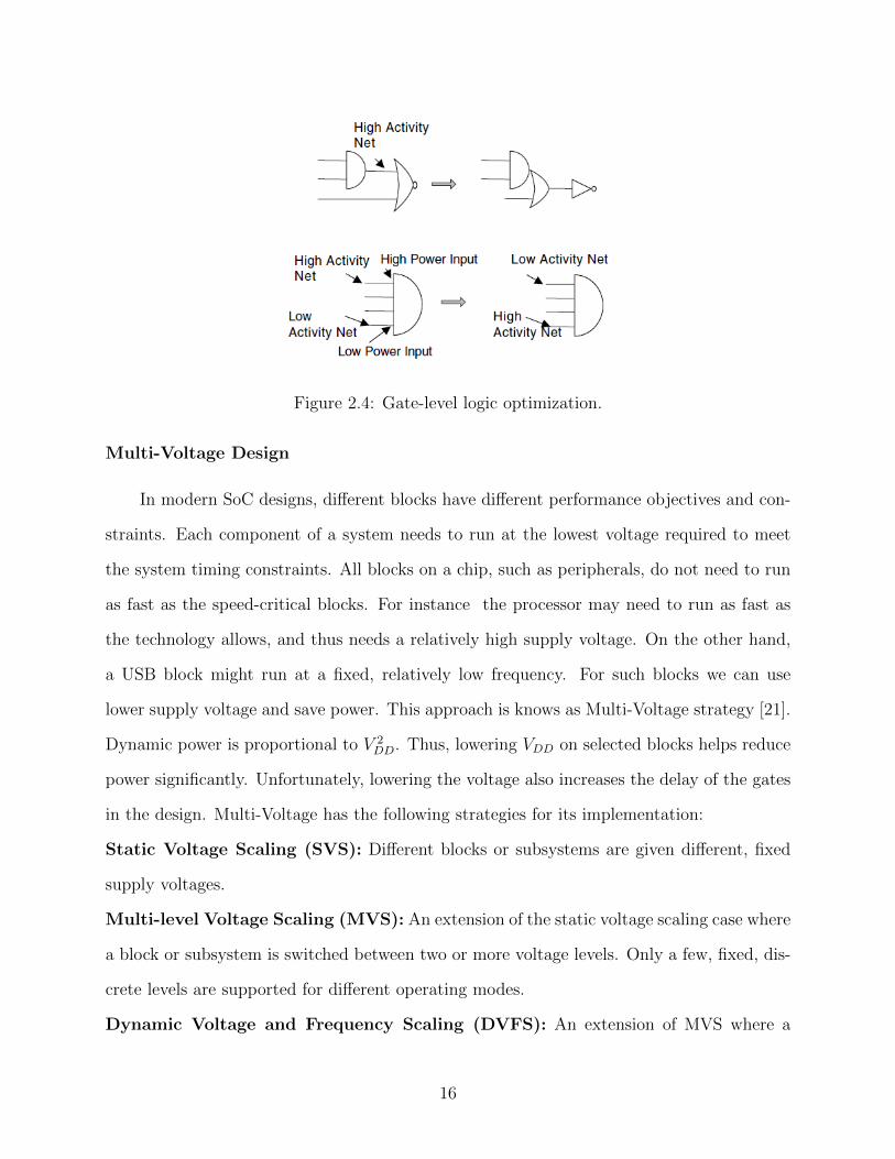
Figure 2.4: Gate-level logic optimization.
Multi-Voltage Design
In modern SoC designs, different blocks have different performance objectives and con-
straints. Each component of a system needs to run at the lowest voltage required to meet
the system timing constraints. All blocks on a chip, such as peripherals, do not need to run
as fast as the speed-critical blocks. For instance the processor may need to run as fast as
the technology allows, and thus needs a relatively high supply voltage. On the other hand,
a USB block might run at a fixed, relatively low frequency. For such blocks we can use
lower supply voltage and save power. This approach is knows as Multi-Voltage strategy [21].
Dynamic power is proportional to V 2DD. Thus, lowering VDD on selected blocks helps reduce
power significantly. Unfortunately, lowering the voltage also increases the delay of the gates
in the design. Multi-Voltage has the following strategies for its implementation:
Static Voltage Scaling (SVS): Different blocks or subsystems are given different, fixed
supply voltages.
Multi-level Voltage Scaling (MVS): An extension of the static voltage scaling case where
a block or subsystem is switched between two or more voltage levels. Only a few, fixed, dis-
crete levels are supported for different operating modes.
Dynamic Voltage and Frequency Scaling (DVFS): An extension of MVS where a
16
larger number of voltage levels are dynamically switched to follow changing workloads. Dy-
namic Voltage and Frequency Scaling (DVFS) is a highly effective method to minimize the
energy dissipation and maximize the battery service time, without any appreciable degra-
dation in the quality of service (QoS) [37]. Although the DVFS method is currently a very
effective way to reduce the dynamic power, it is expected to become less effective as the
process technology scales down. The current trend of lowering the supply voltage in each
generation decreases the leeway available for changing the supply voltage [35].
Adaptive Voltage Scaling (AVS): An extension of DVFS where a control loop is used
to adjust the voltage.
Voltage Scaling
Voltage Scaling is an aggressive technique for dynamic power reduction by reducing the
supply voltage and clock frequency based on workload [36]. For example processors can be
provided a high supply voltage and correspondingly high clock frequency during tasks that
require peak performance. For tasks that require lower performance, power can be saved
by providing a lower voltage and slower clock. This approach is known as voltage scaling.
It can be effective where there is significant voltage headroom. It can be applicable to the
Low-Leakage technology nodes, since these run at higher voltage than the equivalent generic
or high-speed processes. Ignoring the effects of leakage power, clocking a block at half the
frequency halves the dynamic power but takes twice as long to complete the work. Where
scaling the voltage is possible the quadratic dynamic power reduction permits energy savings
to accumulate over the duration of the task. However, the static leakage power cannot of
course be ignored. Reducing the frequency and taking longer to complete a unit of work
also means that the active leakage will be scaled in proportion to the inverse of frequency.
In addition, each voltage scaled block requires additional power rail and all regulated supply
rails have some lost efficiency from generating that voltage with real world power controllers.
Voltage scaling introduces complications into both the system design and the implementation
17
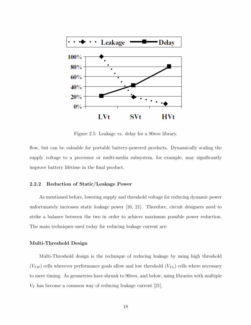
Figure 2.5: Leakage vs. delay for a 90nm library.
flow, but can be valuable for portable battery-powered products. Dynamically scaling the
supply voltage to a processor or multi-media subsystem, for example, may significantly
improve battery lifetime in the final product.
2.2.2 Reduction of Static/Leakage Power
As mentioned before, lowering supply and threshold voltage for reducing dynamic power
unfortunately increases static leakage power [16, 21]. Therefore, circuit designers need to
strike a balance between the two in order to achieve maximum possible power reduction.
The main techniques used today for reducing leakage current are:
Multi-Threshold Design
Multi-Threshold design is the technique of reducing leakage by using high threshold
(VTH) cells wherever performance goals allow and low threshold (VTL) cells where necessary
to meet timing. As geometries have shrunk to 90nm, and below, using libraries with multiple
VT has become a common way of reducing leakage current [21].
18
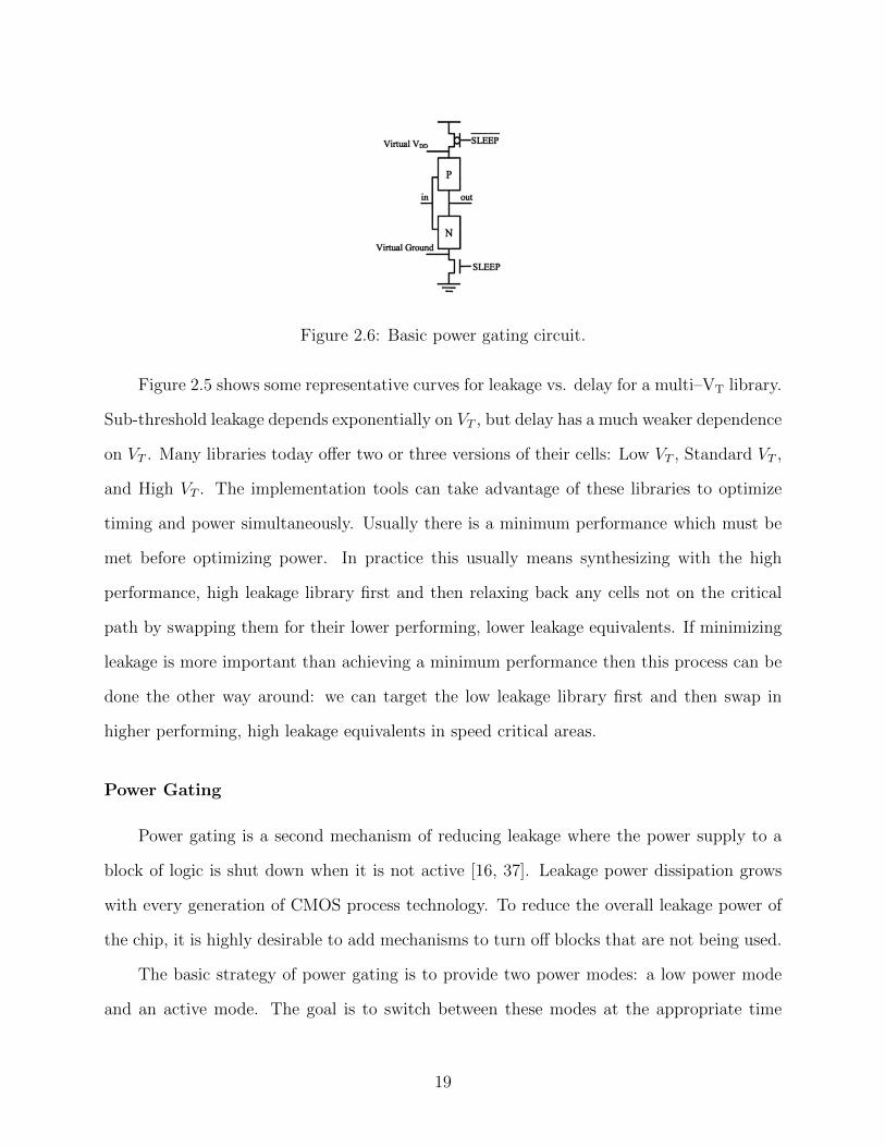
Figure 2.6: Basic power gating circuit.
Figure 2.5 shows some representative curves for leakage vs. delay for a multi–VT library.
Sub-threshold leakage depends exponentially on VT , but delay has a much weaker dependence
on VT . Many libraries today offer two or three versions of their cells: Low VT , Standard VT ,
and High VT . The implementation tools can take advantage of these libraries to optimize
timing and power simultaneously. Usually there is a minimum performance which must be
met before optimizing power. In practice this usually means synthesizing with the high
performance, high leakage library first and then relaxing back any cells not on the critical
path by swapping them for their lower performing, lower leakage equivalents. If minimizing
leakage is more important than achieving a minimum performance then this process can be
done the other way around: we can target the low leakage library first and then swap in
higher performing, high leakage equivalents in speed critical areas.
Power Gating
Power gating is a second mechanism of reducing leakage where the power supply to a
block of logic is shut down when it is not active [16, 37]. Leakage power dissipation grows
with every generation of CMOS process technology. To reduce the overall leakage power of
the chip, it is highly desirable to add mechanisms to turn off blocks that are not being used.
The basic strategy of power gating is to provide two power modes: a low power mode
and an active mode. The goal is to switch between these modes at the appropriate time
19
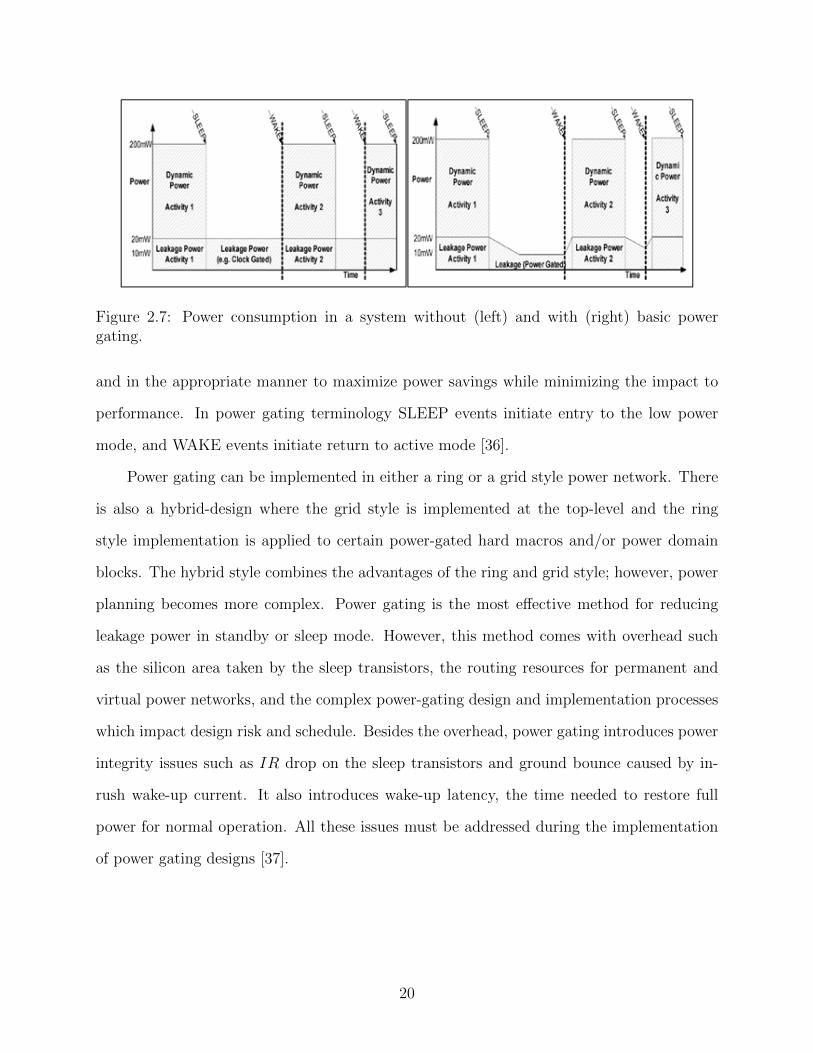
Figure 2.7: Power consumption in a system without (left) and with (right) basic powergating.
and in the appropriate manner to maximize power savings while minimizing the impact to
performance. In power gating terminology SLEEP events initiate entry to the low power
mode, and WAKE events initiate return to active mode [36].
Power gating can be implemented in either a ring or a grid style power network. There
is also a hybrid-design where the grid style is implemented at the top-level and the ring
style implementation is applied to certain power-gated hard macros and/or power domain
blocks. The hybrid style combines the advantages of the ring and grid style; however, power
planning becomes more complex. Power gating is the most effective method for reducing
leakage power in standby or sleep mode. However, this method comes with overhead such
as the silicon area taken by the sleep transistors, the routing resources for permanent and
virtual power networks, and the complex power-gating design and implementation processes
which impact design risk and schedule. Besides the overhead, power gating introduces power
integrity issues such as IR drop on the sleep transistors and ground bounce caused by in-
rush wake-up current. It also introduces wake-up latency, the time needed to restore full
power for normal operation. All these issues must be addressed during the implementation
of power gating designs [37].
20
Variable Threshold CMOS (VT-CMOS)
Variable Threshold CMOS is another effective way of mitigating standby leakage power.
By applying a reverse bias voltage to the substrate, it is possible to reduce the value of the
term (VGS − VT ), effectively increasing VT . This approach can reduce the standby leakage
by up to three orders of magnitude. However, V T −CMOS adds complexity to the library
and requires two additional power networks to separately control the voltage applied to the
wells. Unfortunately, the effectiveness of reverse body bias has been shown to be decreasing
with scaling technology [21].
Stack Effect
The Stack Effect, or self-reverse bias, can reduce sub-threshold leakage when more than
one transistor in the stack is turned off. This is primarily because the small amount of sub-
threshold leakage causes the intermediate nodes between the stacked transistors to float away
from the power/ground rail. The reduced body-source potential results in a slightly negative
gate-source drain voltage. Thus, it reduces the value of the term (VGS − VT ), effectively
increasing VT and reducing the sub-threshold leakage. The leakage of a two transistor stack
has been shown to be an order of magnitude less than that of a single transistor [29]. This
stacking effect makes the leakage of a logic gate highly dependent on its inputs [21].
Long Channel Devices
From the equation for sub-threshold current, it is clear that using non-minimum length
channels will reduce leakage. Unfortunately, long channel devices have lower dynamic cur-
rent, degrading performance. They are also larger and therefore have greater gate capac-
itance, which has an adverse effect on dynamic power consumption and further degrades
performance. There may not be a reduction in total power dissipation unless the switching
activity of the long channel devices is low. Therefore, switching activity and performance
goals must be taken in to account when using long channel devices [21].
21

Chapter 3
Present Day On-Chip Power Distribution Network
An on-chip power grid provides the voltage supply for all integrated devices on a silicon
chip. It is an important component that directly impacts chip functionality of today’s large-
scale integrated circuits (e.g., [21]). Power distribution used to be an afterthought in the
design process before the issues of deep sub-micron brought in new challenges [14] . As the
power density of high-performance ICs is continuously increasing, the on-chip power grid
network is becoming increasingly complex. Though analyzing the distribution network is
emerging as a challenging task, power grid analysis has become a critical design task. An
inadequate or poorly-designed power grid will result in excessive drop and fluctuation in
the voltages supplied to devices, triggering performance degradation and signal integrity
problems [33, 43].
The power distribution subsystem of a chip consists of metal wires or planes on the chip.
It also includes bypass capacitors to supply the instantaneous current requirements of the
system. According to [46], an ideal power distribution network has the following properties:
• Maintains a stable voltage with little noise
• Satisfies average and peak power demands
• Provides current return paths for signals
• Avoids wear out from electromigration and self-heating
• Consumes minimal chip area and wiring
• Easy to lay out
22
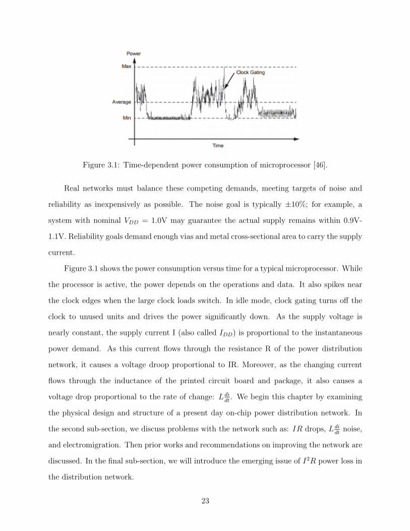
Figure 3.1: Time-dependent power consumption of microprocessor [46].
Real networks must balance these competing demands, meeting targets of noise and
reliability as inexpensively as possible. The noise goal is typically ±10%; for example, a
system with nominal VDD = 1.0V may guarantee the actual supply remains within 0.9V-
1.1V. Reliability goals demand enough vias and metal cross-sectional area to carry the supply
current.
Figure 3.1 shows the power consumption versus time for a typical microprocessor. While
the processor is active, the power depends on the operations and data. It also spikes near
the clock edges when the large clock loads switch. In idle mode, clock gating turns off the
clock to unused units and drives the power significantly down. As the supply voltage is
nearly constant, the supply current I (also called IDD) is proportional to the instantaneous
power demand. As this current flows through the resistance R of the power distribution
network, it causes a voltage droop proportional to IR. Moreover, as the changing current
flows through the inductance of the printed circuit board and package, it also causes a
voltage drop proportional to the rate of change: Ldidt
. We begin this chapter by examining
the physical design and structure of a present day on-chip power distribution network. In
the second sub-section, we discuss problems with the network such as: IR drops, Ldidt
noise,
and electromigration. Then prior works and recommendations on improving the network are
discussed. In the final sub-section, we will introduce the emerging issue of I2R power loss in
the distribution network.
23
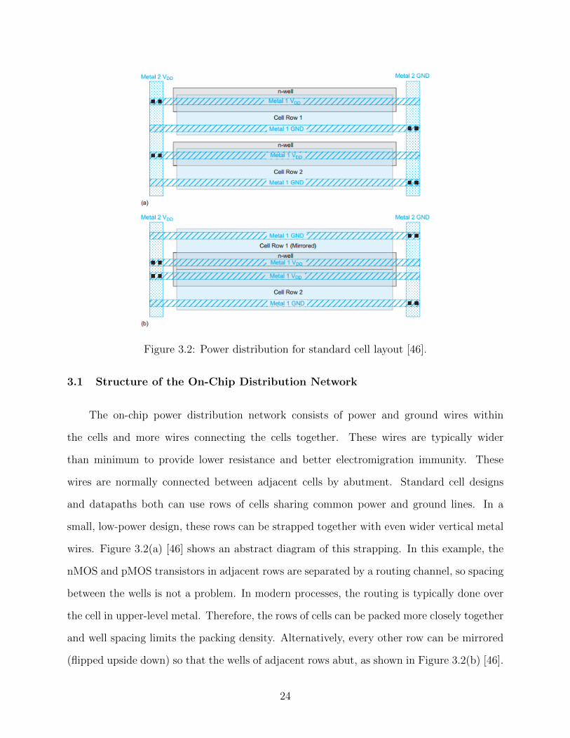
Figure 3.2: Power distribution for standard cell layout [46].
3.1 Structure of the On-Chip Distribution Network
The on-chip power distribution network consists of power and ground wires within
the cells and more wires connecting the cells together. These wires are typically wider
than minimum to provide lower resistance and better electromigration immunity. These
wires are normally connected between adjacent cells by abutment. Standard cell designs
and datapaths both can use rows of cells sharing common power and ground lines. In a
small, low-power design, these rows can be strapped together with even wider vertical metal
wires. Figure 3.2(a) [46] shows an abstract diagram of this strapping. In this example, the
nMOS and pMOS transistors in adjacent rows are separated by a routing channel, so spacing
between the wells is not a problem. In modern processes, the routing is typically done over
the cell in upper-level metal. Therefore, the rows of cells can be packed more closely together
and well spacing limits the packing density. Alternatively, every other row can be mirrored
(flipped upside down) so that the wells of adjacent rows abut, as shown in Figure 3.2(b) [46].
24
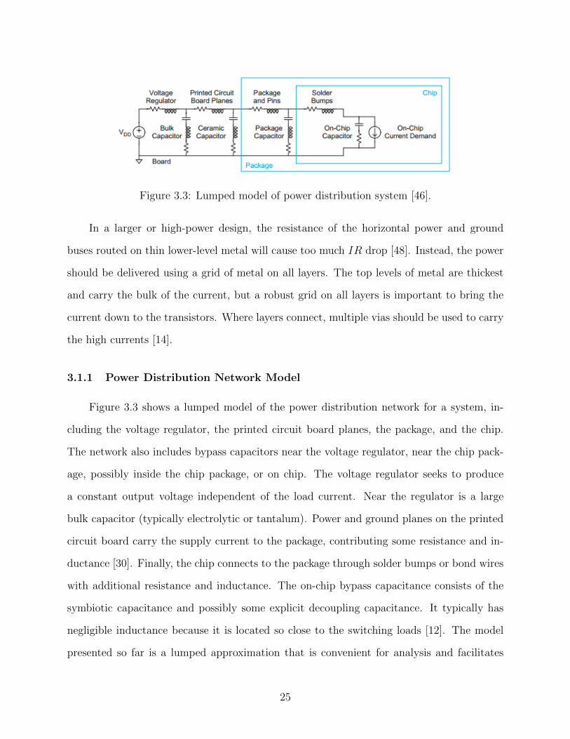
Figure 3.3: Lumped model of power distribution system [46].
In a larger or high-power design, the resistance of the horizontal power and ground
buses routed on thin lower-level metal will cause too much IR drop [48]. Instead, the power
should be delivered using a grid of metal on all layers. The top levels of metal are thickest
and carry the bulk of the current, but a robust grid on all layers is important to bring the
current down to the transistors. Where layers connect, multiple vias should be used to carry
the high currents [14].
3.1.1 Power Distribution Network Model
Figure 3.3 shows a lumped model of the power distribution network for a system, in-
cluding the voltage regulator, the printed circuit board planes, the package, and the chip.
The network also includes bypass capacitors near the voltage regulator, near the chip pack-
age, possibly inside the chip package, or on chip. The voltage regulator seeks to produce
a constant output voltage independent of the load current. Near the regulator is a large
bulk capacitor (typically electrolytic or tantalum). Power and ground planes on the printed
circuit board carry the supply current to the package, contributing some resistance and in-
ductance [30]. Finally, the chip connects to the package through solder bumps or bond wires
with additional resistance and inductance. The on-chip bypass capacitance consists of the
symbiotic capacitance and possibly some explicit decoupling capacitance. It typically has
negligible inductance because it is located so close to the switching loads [12]. The model
presented so far is a lumped approximation that is convenient for analysis and facilitates
25

Figure 3.4: On-chip power grid [46].
gaining intuition about chip behavior. Chip designers also are concerned about the variation
in supply voltage across the chip. This requires a distributed model, which we can approxi-
mate with a mesh of small elements as shown in Figure 3.4 [18, 46]. The mesh represents the
resistance and inductance of the on-chip power supply grid. Symbiotic or explicit decoupling
capacitors are distributed across the chip. At each node, a current source represents the
local current demand of the circuitry. The solder bumps or bond wires to the package are
modeled with additional resistance and inductance. In this model, the package is treated as
a perfect VDD connected to the corners of the grid.
The power grid extends across the entire chip or voltage domain. Ultimately, it must
connect to the package through the I/O pads. When a pad ring is used, the connections are
all near the periphery of the chip. Thus, the biggest IR drops occur near the center of the
chip where the current flows through the longest wires and greatest resistance. C4 solder
bumps distributed across the die are much better for power distribution because they can
deliver the current from the low-resistance power plane in the package directly to the area
of the chip where the current is needed. Thus, less on-chip metal resources are needed for
power distribution. The power system is usually done hierarchically to manage complexity,
but in the end the overall design must satisfy the noise budgets specified for the chip[15].
26
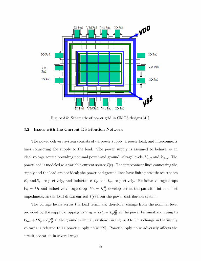
Figure 3.5: Schematic of power grid in CMOS designs [41].
3.2 Issues with the Current Distribution Network
The power delivery system consists of - a power supply, a power load, and interconnects
lines connecting the supply to the load. The power supply is assumed to behave as an
ideal voltage source providing nominal power and ground voltage levels, VDD and VGnd. The
power load is modeled as a variable current source I(t). The interconnect lines connecting the
supply and the load are not ideal; the power and ground lines have finite parasitic resistances
Rp andRg, respectively, and inductance Lp and Lg, respectively. Resistive voltage drops
VR = IR and inductive voltage drops VL = LdIdt
develop across the parasitic interconnect
impedances, as the load draws current I(t) from the power distribution system.
The voltage levels across the load terminals, therefore, change from the nominal level
provided by the supply, dropping to VDD − IRp − LpdIdt
at the power terminal and rising to
VGnd +IRg +LgdIdt
at the ground terminal, as shown in Figure 3.6. This change in the supply
voltages is referred to as power supply noise [29]. Power supply noise adversely affects the
circuit operation in several ways.
27
Figure 3.6: Power delivery system [46].
3.2.1 IR Drops
Due to the resistance of the interconnects constituting the network, there occurs a
voltage drop across the network; this is commonly referred to as the IR drop [46, 47].
IR drop is predominantly caused by the parasitic resistance of metal wires constituting
the on-chip power distribution network [34]. The resistance of the complete power supply
network includes the resistance of the on-chip wires and vias, the resistance of the bond
wires or solder bumps on the package, the resistance of the package planes or traces, and
the resistance of the printed circuit board planes. Because the package and printed circuit
board typically use copper that is much thicker and wider than on-chip wires, the on-chip
network dominates the resistive drop. IR drops arise from both average and instantaneous
current requirements. The instantaneous current may be much larger than the average drop
because current draw tends to locally spike near the clock edge when many registers and
gates switch simultaneously. Bypass capacitance near the switching gates can supply much of
this instantaneous current, so a well-bypassed power supply network only needs low enough
resistance to deliver the average current demand, not necessarily the peak.
3.2.2 LdIdt
Noise
Although the resistance of package is quite small, the inductance of package leads is
significant, which causes a voltage drop at the pad locations due to time-varying currents
drawn by devices on the die. This voltage drop is referred to as the dIdt
drop or LdIdt
drop [34].
28
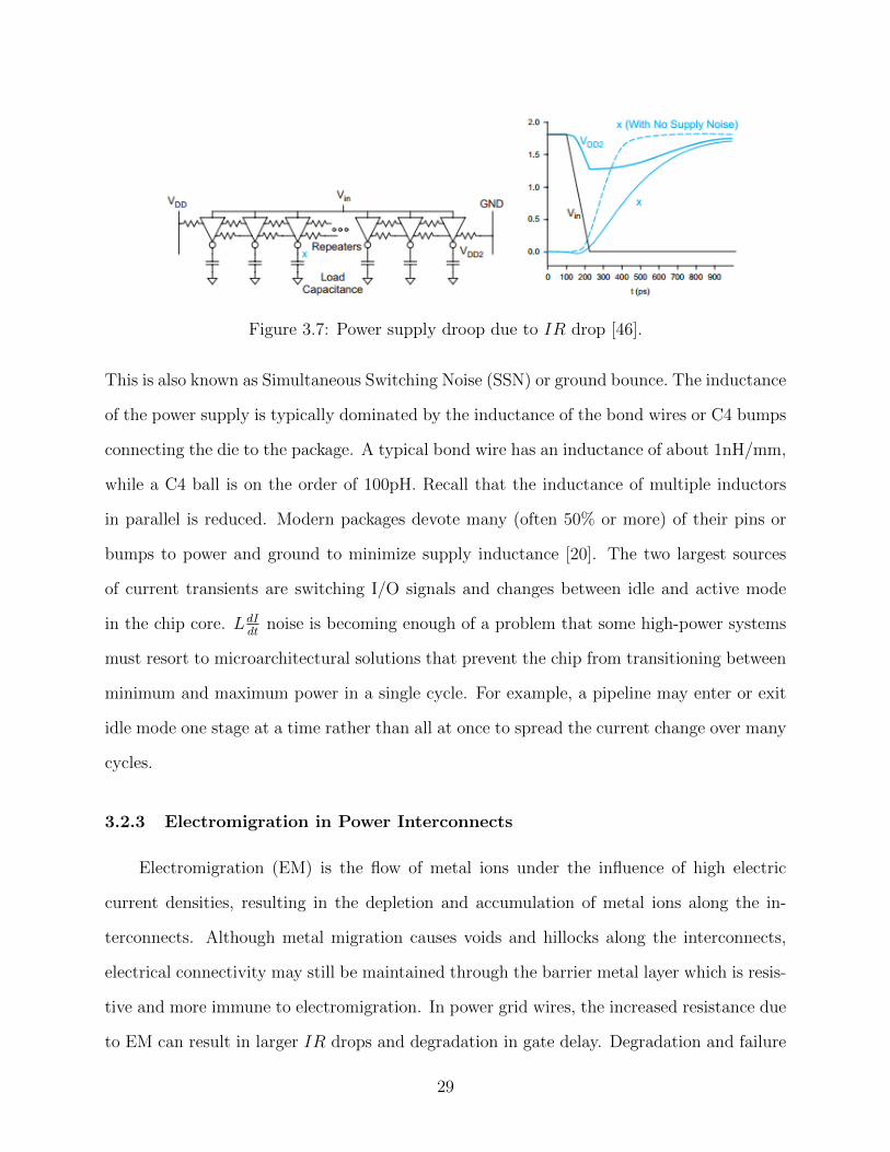
Figure 3.7: Power supply droop due to IR drop [46].
This is also known as Simultaneous Switching Noise (SSN) or ground bounce. The inductance
of the power supply is typically dominated by the inductance of the bond wires or C4 bumps
connecting the die to the package. A typical bond wire has an inductance of about 1nH/mm,
while a C4 ball is on the order of 100pH. Recall that the inductance of multiple inductors
in parallel is reduced. Modern packages devote many (often 50% or more) of their pins or
bumps to power and ground to minimize supply inductance [20]. The two largest sources
of current transients are switching I/O signals and changes between idle and active mode
in the chip core. LdIdt
noise is becoming enough of a problem that some high-power systems
must resort to microarchitectural solutions that prevent the chip from transitioning between
minimum and maximum power in a single cycle. For example, a pipeline may enter or exit
idle mode one stage at a time rather than all at once to spread the current change over many
cycles.
3.2.3 Electromigration in Power Interconnects
Electromigration (EM) is the flow of metal ions under the influence of high electric
current densities, resulting in the depletion and accumulation of metal ions along the in-
terconnects. Although metal migration causes voids and hillocks along the interconnects,
electrical connectivity may still be maintained through the barrier metal layer which is resis-
tive and more immune to electromigration. In power grid wires, the increased resistance due
to EM can result in larger IR drops and degradation in gate delay. Degradation and failure
29

of a device are very complex and are commonly modeled as statistical phenomena using
empirical models based on experiments and/or simulations. The primary stress factors that
accelerate EM induced degradation and failure of interconnects are the temperature and the
current density through the interconnect [19].
3.2.4 Signal Delay Uncertainty
The drain current of a MOS transistor increases with the voltage difference between
the transistor gate and source. When the rail-to-rail power voltage is reduced due to power
supply variations, the gate-to-source voltage of the nMOS and pMOS transistors is decreased,
thereby lowering the output current of the transistors. The signal delay increases accordingly
as compared to the delay under a nominal power supply voltage. Conversely, a higher power
voltage and a lower ground voltage will shorten the propagation delay. The net effect of the
power noise on the propagation of the clock and data signals is, therefore, an increase in
both delay uncertainty and the delay of the data paths. Consequently, power supply noise
limits the maximum operating frequency of an integrated circuit [38].
3.2.5 On-chip Clock Jitter
A phase-locked loop (PLL) is often used to generate the on-chip clock signal. An on-
chip PLL generates an on-chip clock signal by multiplying the frequency of the system clock
signal. Various changes in the electrical environment of a PLL, power supply level variations
in particular, affect the phase of the on-chip clock signal. A feedback loop within the PLL
controls the phase of the PLL output and aligns the output signal phase with the phase of
the system clock. Ideally, the edges of the on-chip clock signal are at precisely equidistant
time intervals determined by the system clock signal. The closed loop response time of the
PLL is hundreds of nanoseconds. Disturbances of shorter duration than the PLL response
time result in deviations of the on-chip clock phase from the ideal timing. These deviations
30

are referred to as clock jitter. The clock jitter is classified into two types: cycle-to-cycle jitter
and peak-to-peak jitter [38].
3.2.6 Noise Margin Degradation
In digital logic styles with single-ended signaling, the power and ground supply networks
also serve as a voltage reference for the on-chip signals. If a transmitter communicates a low
voltage state, the output of the transmitter is connected to the ground distribution network.
Alternatively, the output is connected to the power distribution network to communicate
the high voltage state. At the receiver end of the communication line, the output voltage
of the transmitter is compared to the power or ground voltage local to the receiver. Spatial
variations in the supply voltage create a discrepancy between the power and ground voltage
levels at the transmitter and receiver ends of the communication line. The power noise
induced uncertainty in these reference voltages degrades the noise margins of the on-chip
signals. As the operating speed of integrated circuits rise, crosstalk noise among on-chip
signals has increased. Sufficient noise margins for the on-chip signals have therefore become
a design issue of primary importance [38].
3.3 Prior Work on Improving the Network
Significant work is being done to improve and develop the on-chip power distribution
network. Dynamic IR drop and LdIdt
are by far the main problems with present day power
distribution network. In fact, the other issues faced by the network are direct or indirect
byproducts of these two. Following are the two major methods used in the industry to
minimize the problems:
3.3.1 Wire Sizing
Wire-sizing is probably the most common method to reduce the overall peak voltage
drop by reducing the resistivity of interconnect lines. Although with up-sizing of the widths
31
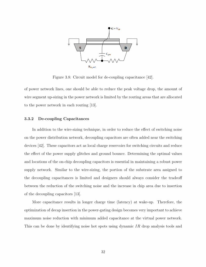
Figure 3.8: Circuit model for de-coupling capacitance [42].
of power network lines, one should be able to reduce the peak voltage drop, the amount of
wire segment up-sizing in the power network is limited by the routing areas that are allocated
to the power network in each routing [13].
3.3.2 De-coupling Capacitances
In addition to the wire-sizing technique, in order to reduce the effect of switching noise
on the power distribution network, decoupling capacitors are often added near the switching
devices [42]. These capacitors act as local charge reservoirs for switching circuits and reduce
the effect of the power supply glitches and ground bounce. Determining the optimal values
and locations of the on-chip decoupling capacitors is essential in maintaining a robust power
supply network. Similar to the wire-sizing, the portion of the substrate area assigned to
the decoupling capacitances is limited and designers should always consider the tradeoff
between the reduction of the switching noise and the increase in chip area due to insertion
of the decoupling capacitors [13].
More capacitance results in longer charge time (latency) at wake-up. Therefore, the
optimization of decap insertion in the power-gating design becomes very important to achieve
maximum noise reduction with minimum added capacitance at the virtual power network.
This can be done by identifying noise hot spots using dynamic IR drop analysis tools and
32
then inserting just enough capacitance at the hot spots to reduce the noises meeting defined
noise target. Recommendations:
• Add as much decoupling capacitance as permitted in the permanent power network
at positions close to the switch cells. This achieves the maximum effectiveness and
minimum impact on the wake-up latency and in-rush current. It is convenient to
integrate the decap into the switch cell to simplify decap insertion.
• To fix dynamic IR drop violations in the post-layout stage, it is preferable to add
decoupling capacitance to the permanent power network close to the violation spots, if
the violations are related to the permanent power network. The rest of the violations
have to be fixed by adding decap to the virtual power network at the violation spots.
Apart from this, as possible solutions for static IR drop [14], suggests the following:
• Rearrange blocks
• More VDD pins
• Connect the bottom portion of grid to the top portion
Although, these methods alleviate the situation, the problem of supply voltage droop is
not really solved. To ensure all the loads in the grid network get the supply voltage required
for desired performance, sufficient number of repeaters/feed points are added to the network.
3.4 I2R Power Loss across the Distribution Network
While extensive research is being carried out to find power reduction techniques for
different levels of design abstraction, the prospect of potential power savings in the power
distribution network itself seems to lack attention. We know that, power loss in a resistive
conductor is: P = I2R, where R is the resistance of the wire. Now, just like IR voltage drop
33
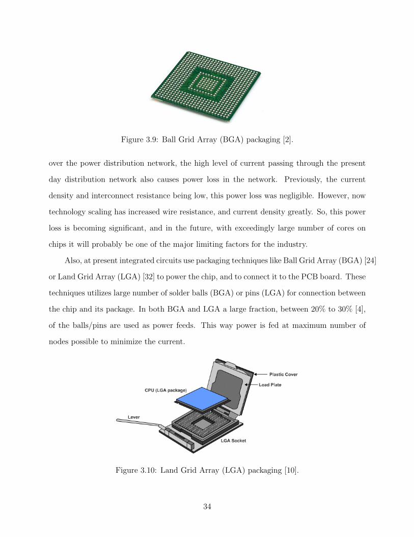
Figure 3.9: Ball Grid Array (BGA) packaging [2].
over the power distribution network, the high level of current passing through the present
day distribution network also causes power loss in the network. Previously, the current
density and interconnect resistance being low, this power loss was negligible. However, now
technology scaling has increased wire resistance, and current density greatly. So, this power
loss is becoming significant, and in the future, with exceedingly large number of cores on
chips it will probably be one of the major limiting factors for the industry.
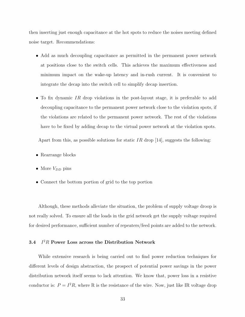
Also, at present integrated circuits use packaging techniques like Ball Grid Array (BGA) [24]
or Land Grid Array (LGA) [32] to power the chip, and to connect it to the PCB board. These
techniques utilizes large number of solder balls (BGA) or pins (LGA) for connection between
the chip and its package. In both BGA and LGA a large fraction, between 20% to 30% [4],
of the balls/pins are used as power feeds. This way power is fed at maximum number of
nodes possible to minimize the current.
Figure 3.10: Land Grid Array (LGA) packaging [10].
34

However, as we start to get SoCs with hundreds and possibly thousands of cores on
them, maintaining this ratio of power pins will become physically impractical. This will
increase the current flowing through the circuit as each pin will have supply power to larger
loads. Thereby this will also increase I2R loss.
We expect that, by decreasing the current flowing through the network, our proposed
high-voltage scheme will increase the efficiency of power delivery significantly and solve the
problem for future.
35
Chapter 4
High-Voltage On-Chip Power Distribution Network
We have seen that an on-chip power distribution network is predominantly resistive
in nature. Therefore, as current flows through, the network causes voltage drop (IR) and
power loss (I2R). As a result of continuous technology scaling we are now well within the
much sought nanometer paradigm. But, this technological progress is strongly affecting
the on-chip power distribution network, and rather adversely. As technology is scaling, the
inherent resistance of interconnect wires is going up, and current density is increasing. This
is making the voltage drop and the power loss issue worse. The voltage drop issue is well
established and a lot work is going under to solve/improve it. However, though the power
is quadratically related to current, the aspect of power loss in the network has not created
much concern in the industry or in the academia. But, with exceedingly large and complex
circuits like thousand core SoCs within sight, in order to keep Moore’s Law going, we need to
deal with this issue right now. In this chapter, we first briefly state what inspired us to think
about the novel concept of High-Voltage On-Chip power distribution network. Then, DC-DC
converters, the essential device on which our proposed scheme is based, is discussed. After
that we introduce the construction of our proposed power distribution network. Finally, we
talk about expected power saving and other probable benefits from the scheme.
4.1 Inspiration: Joules Law and Long-Distance Power Transmission Grid
Joules First Law or The Law of Resistive Heating:
Passage of an electric current through a conductor releases heat, and the amount of heat
released is proportional to the square of the current such that:
36
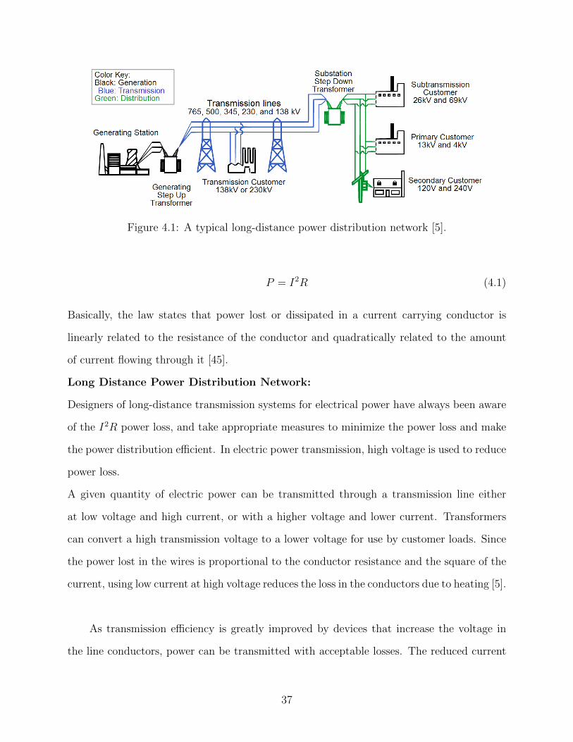
Figure 4.1: A typical long-distance power distribution network [5].
P = I2R (4.1)
Basically, the law states that power lost or dissipated in a current carrying conductor is
linearly related to the resistance of the conductor and quadratically related to the amount
of current flowing through it [45].
Long Distance Power Distribution Network:
Designers of long-distance transmission systems for electrical power have always been aware
of the I2R power loss, and take appropriate measures to minimize the power loss and make
the power distribution efficient. In electric power transmission, high voltage is used to reduce
power loss.
A given quantity of electric power can be transmitted through a transmission line either
at low voltage and high current, or with a higher voltage and lower current. Transformers
can convert a high transmission voltage to a lower voltage for use by customer loads. Since
the power lost in the wires is proportional to the conductor resistance and the square of the
current, using low current at high voltage reduces the loss in the conductors due to heating [5].
As transmission efficiency is greatly improved by devices that increase the voltage in
the line conductors, power can be transmitted with acceptable losses. The reduced current
37
flowing through the line reduces the heating losses in the conductors. According to Joule’s
Law, energy losses are directly proportional to the square of the current. For example,
raising the voltage by a factor of 10 reduces the current by a corresponding factor of 10 and
therefore the I2R losses by a factor of 100, provided the same sized conductors are used
in both cases [5]. This increase of voltage is usually achieved in AC circuits by using a
step-up transformer. High-voltage direct current (HVDC) is used to transmit large amounts
of power over long distances or for interconnections between asynchronous grids. HVDC
systems require relatively costly conversion equipment which may be economically justified
for particular projects such as submarine cables and longer distance high capacity point
to point transmission but are infrequently used at present [5]. Transmitting electricity at
high voltage reduces the fraction of energy lost to resistance, which varies depending on the
specific conductors, the current flowing and the length of the transmission line. For example,
a 100 mile 765 kV line carrying 1000 MW of energy can have losses of 1.1% to 0.5%. A 345 kV
line carrying the same load across the same distance has losses of 4.2% [1].
4.2 DC-DC Voltage Converters
While AC-DC converters convert Alternating Current (AC) to Direct Current (DC),
DC-DC converters can be approximately analogous to DC transformers. As transformer
steps up or steps down AC current, DC-DC converters do that for DC current.
4.2.1 Definition
A DC-DC voltage converter/regulator is a circuit that generates a regulated DC output
voltage from a (possibly) unregulated DC input voltage with a different voltage magnitude
and/or polarity [23].
38
4.2.2 Types of Operation
DC-DC converters can carry out 3 types of operation:
Buck Converter: A buck converter is a step-down converter that converts a higher input
voltage to a fixed lower output voltage. For our scheme, we are interested in buck convert-
ers [23].
Boost Converter: A boost converter is a step-up converter that converts a lower input
voltage to a fixed higher output voltage [23].
Buck-Boost Converter: A buck-boost converter is a voltage regulator that converts lower
or higher input voltages to a fixed output voltage [23].
4.2.3 Classification of DC-DC Converter Designs
Linear DC-DC Converters
Linear regulators are used to generate a DC output voltage with a lower magnitude
and the same polarity as compared to a DC input voltage. Linear regulators utilize resistive
voltage division to produce an output supply voltage lower than an input supply voltage.
Linear converters have intrinsically low efficiency, particularly if the input-to-output voltage
conversion ratio is high. Linear regulators are found in many types of ICs due to the easy de-
sign, low circuit complexity, and small area consistent with an on-chip implementation [17].
Linear (series-pass) DC-DC converters are popular due to the simple structure and small
physical area. Linear DC-DC converters operate on the principle of resistive voltage divi-
sion. The operation of a simple linear voltage converter is illustrated in Figure 4.2 [23].
As shown in Figure 4.2, in an ideal linear converter, the current supplied to the load
is equal to the current drawn from the primary power supply VDD1. The highest efficiency
39
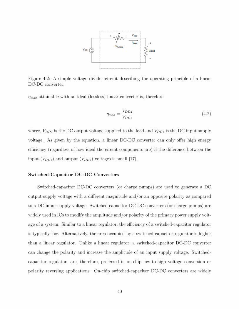
Figure 4.2: A simple voltage divider circuit describing the operating principle of a linearDC-DC converter.
ηmax attainable with an ideal (lossless) linear converter is, therefore
ηmax =VDD2
VDD1
(4.2)
where, VDD2 is the DC output voltage supplied to the load and VDD1 is the DC input supply
voltage. As given by the equation, a linear DC-DC converter can only offer high energy
efficiency (regardless of how ideal the circuit components are) if the difference between the
input (VDD1) and output (VDD2) voltages is small [17] .
Switched-Capacitor DC-DC Converters
Switched-capacitor DC-DC converters (or charge pumps) are used to generate a DC
output supply voltage with a different magnitude and/or an opposite polarity as compared
to a DC input supply voltage. Switched-capacitor DC-DC converters (or charge pumps) are
widely used in ICs to modify the amplitude and/or polarity of the primary power supply volt-
age of a system. Similar to a linear regulator, the efficiency of a switched-capacitor regulator
is typically low. Alternatively, the area occupied by a switched-capacitor regulator is higher
than a linear regulator. Unlike a linear regulator, a switched-capacitor DC-DC converter
can change the polarity and increase the amplitude of an input supply voltage. Switched-
capacitor regulators are, therefore, preferred in on-chip low-to-high voltage conversion or
polarity reversing applications. On-chip switched-capacitor DC-DC converters are widely
40
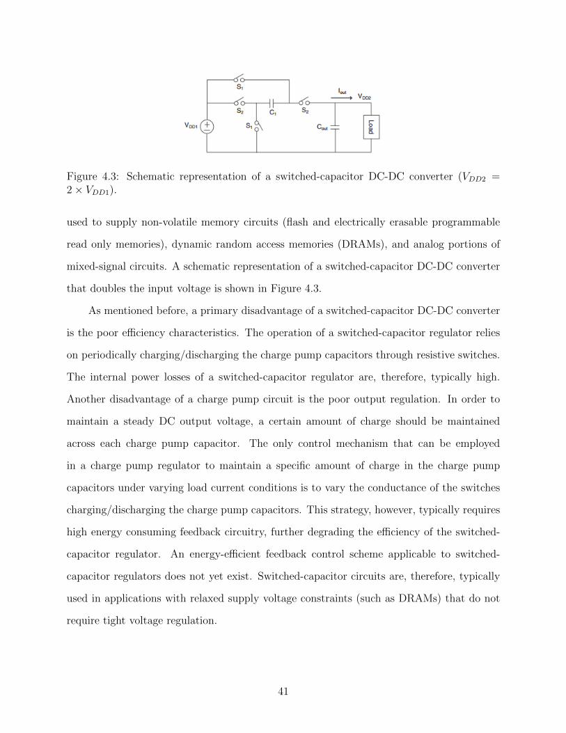
Figure 4.3: Schematic representation of a switched-capacitor DC-DC converter (VDD2 =2× VDD1).
used to supply non-volatile memory circuits (flash and electrically erasable programmable
read only memories), dynamic random access memories (DRAMs), and analog portions of
mixed-signal circuits. A schematic representation of a switched-capacitor DC-DC converter
that doubles the input voltage is shown in Figure 4.3.
As mentioned before, a primary disadvantage of a switched-capacitor DC-DC converter
is the poor efficiency characteristics. The operation of a switched-capacitor regulator relies
on periodically charging/discharging the charge pump capacitors through resistive switches.
The internal power losses of a switched-capacitor regulator are, therefore, typically high.
Another disadvantage of a charge pump circuit is the poor output regulation. In order to
maintain a steady DC output voltage, a certain amount of charge should be maintained
across each charge pump capacitor. The only control mechanism that can be employed
in a charge pump regulator to maintain a specific amount of charge in the charge pump
capacitors under varying load current conditions is to vary the conductance of the switches
charging/discharging the charge pump capacitors. This strategy, however, typically requires
high energy consuming feedback circuitry, further degrading the efficiency of the switched-
capacitor regulator. An energy-efficient feedback control scheme applicable to switched-
capacitor regulators does not yet exist. Switched-capacitor circuits are, therefore, typically
used in applications with relaxed supply voltage constraints (such as DRAMs) that do not
require tight voltage regulation.
41
Switching Regulators
Switching regulators are capable of modifying both the amplitude and polarity of the
input voltages. The primary advantages of a switching regulator are the high conversion
efficiency and good output voltage regulation characteristics as compared to a linear or
switched-capacitor DC-DC converter. The primary drawback of switching regulators, how-
ever, is the inductive elements(inductors and/or transformers) required for energy storage
and filtering. Filter inductors are, to date, prohibitive in the fabrication of an on-chip
switching DC-DC converter.
A switching DC-DC converter generates a DC output supply voltage with a different
magnitude and/or polarity than the DC input voltage. Among DC-DC converter topolo-
gies, switching voltage regulators are the most widely used due to the high efficiency and
good output voltage regulation characteristics. Unlike a linear or switched-capacitor DC-DC
converter, the efficiency of switching DC-DC converter approaches 100% as the transistor
switches are made more ideal.
Switching DC-DC converters can be divided into two primary categories. The first
category of switching DC-DC converters utilizes transformers. Switching DC-DC converters
with transformers are called isolated switching DC-DC converters. The primary use of
transformers in switching DC-DC converters is the DC isolation of the input and output
grounds. Provided that the primary power supply operates at a relatively high voltage
and/or is noisy, isolation of the load from the input supply is necessary to maintain reliable
operation of the load. Another advantage of isolated switching DC-DC converters is the
relatively easy and straightforward generation of multiple DC output voltages from a single
DC input voltage. A single control circuit can be used to generate several different DC
supply voltages by simply utilizing a multiple winding transformer, provided that the voltage
regulation requirements of the load circuits are not excessively tight.
A second category of switching DC-DC converters utilizes inductors (no isolating trans-
formers) for energy storage and signal filtering. These switching DC-DC converters without
42
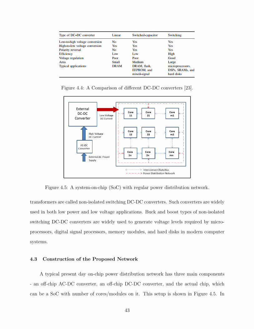
Figure 4.4: A Comparison of different DC-DC converters [23].
Figure 4.5: A system-on-chip (SoC) with regular power distribution network.
transformers are called non-isolated switching DC-DC converters. Such converters are widely
used in both low power and low voltage applications. Buck and boost types of non-isolated
switching DC-DC converters are widely used to generate voltage levels required by micro-
processors, digital signal processors, memory modules, and hard disks in modern computer
systems.
4.3 Construction of the Proposed Network
A typical present day on-chip power distribution network has three main components
- an off-chip AC-DC converter, an off-chip DC-DC converter, and the actual chip, which
can be a SoC with number of cores/modules on it. This setup is shown in Figure 4.5. In
43
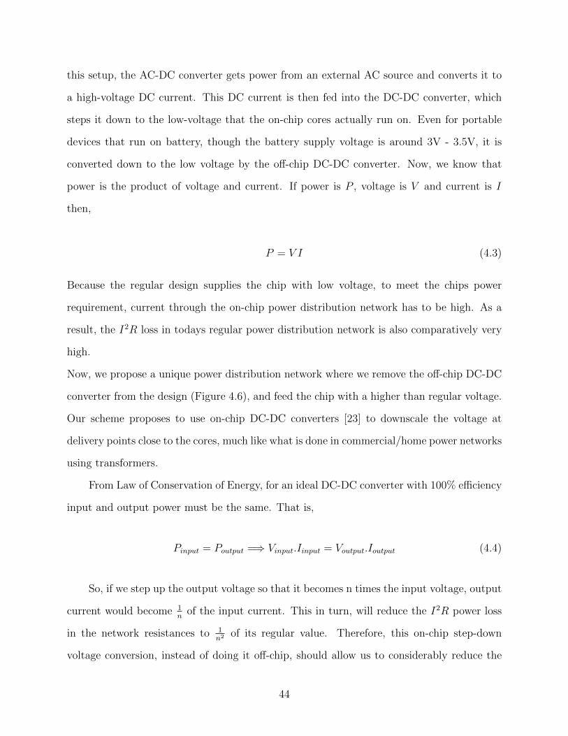
this setup, the AC-DC converter gets power from an external AC source and converts it to
a high-voltage DC current. This DC current is then fed into the DC-DC converter, which
steps it down to the low-voltage that the on-chip cores actually run on. Even for portable
devices that run on battery, though the battery supply voltage is around 3V - 3.5V, it is
converted down to the low voltage by the off-chip DC-DC converter. Now, we know that
power is the product of voltage and current. If power is P , voltage is V and current is I
then,
P = V I (4.3)
Because the regular design supplies the chip with low voltage, to meet the chips power
requirement, current through the on-chip power distribution network has to be high. As a
result, the I2R loss in todays regular power distribution network is also comparatively very
high.
Now, we propose a unique power distribution network where we remove the off-chip DC-DC
converter from the design (Figure 4.6), and feed the chip with a higher than regular voltage.
Our scheme proposes to use on-chip DC-DC converters [23] to downscale the voltage at
delivery points close to the cores, much like what is done in commercial/home power networks
using transformers.
From Law of Conservation of Energy, for an ideal DC-DC converter with 100% efficiency
input and output power must be the same. That is,
Pinput = Poutput =⇒ Vinput.Iinput = Voutput.Ioutput (4.4)
So, if we step up the output voltage so that it becomes n times the input voltage, output
current would become 1n
of the input current. This in turn, will reduce the I2R power loss
in the network resistances to 1n2 of its regular value. Therefore, this on-chip step-down
voltage conversion, instead of doing it off-chip, should allow us to considerably reduce the
44
Figure 4.6: A system-on-chip (SoC) with high-voltage power distribution network.
current (I) flowing through the on-chip power network. As a result, we expect our scheme
to save significant amount of power by reducing the I2R power loss in the power distribution
network.
4.4 Selection of the Distribution Voltage
We have seen in the preceding sub-section that power being the product of voltage and
current, for a fixed load power if we step up voltage by n times, the resulting current becomes
1n
of the original value. The result is I2R power loss reduces by a factor of 1n2 .
So, if there is no limiting factor on the distribution voltage, then we increase power
saving by increasing distribution voltage. This power saving results in increased efficiency
of the circuit. For a distribution voltage V , if load power is PLoad(V ), Power lost in the grid
is PGrid(V ) and total power is PTotal(V ), then,
Efficiency =PLoad(V )
PTotal(V )
× 100 (4.5)
=PLoad(V )
PLoad(V ) + PGrid(V )
× 100 (4.6)
45
Now, if distribution voltage is increased from V to nV , then power lost in grid, PGrid(V )
will decrease toPGrid(V )
n2 . So, the efficiency would changed to
Efficiency =PLoad(V )
PLoad(V ) +PGrid(V )
n2
× 100 (4.7)
=n2PLoad(V )
n2PLoad(V ) + PGrid(V )
× 100 (4.8)
Therefore, if n is increased towards infinity efficiency of the circuit will approach 100%. We
can use this characteristics to increase efficiency of a fixed sized circuit. We will attempt
to verify this relationship between distribution voltage and efficiency from our experimental
results.
However, in reality there are several technical factors like dielectric breakdown etc. that
limit the upper boundary of the distribution voltage
4.5 Advantages of the Scheme
Our proposed scheme lowers the current flow through the distribution network to a
fraction of its regular value by stepping up the supply voltage. This current reduction is the
source of all the expected advantages of the scheme listed below.
Power Saving and Increased Efficiency:
The first and the most anticipated reward from a possible implementation of this scheme is
power saving. We have seen from Joule’s Law that resistive power loss (I2R) has a quadratic
relation with current. Also, due to Law of Conservation of Energy, with ideal DC-DC
converters stepping up the supply voltage by n times should give us power reduction of 1n2 .
With non-ideal DC-DC converters this power saving will be less. However, with DC-DC
converters with decent efficiency, we can expect significant reduction in power loss over the
network. In other words, efficiency of the chips will increase vastly.
46

Apart from reducing power loss and increasing circuit efficiency, the proposed method
is also expected to alleviate the following issues with present day on-chip power distribution
networks.
Reduced IR drop: As current through the network reduces to a fraction of its original
value, voltage (IR) drop across the network would automatically reduce. Moreover, with the
DC-DC converters adjacent to the loads, the overall issue of loads getting required voltage
for optimal performance would probably become negligible. Whatever voltage drop occurs
across the nodes, the converter would ensure that the loads are fed with optimal supply
voltage (e.g., 1V).
Reduced Electromigration: By reducing current the scheme should also alleviate the
electromigration problem in the power distribution network.
Reduced Signal Delay Uncertainty: As the proposed scheme reduces IR drop, it should
reduce the Signal Delay Uncertainty problem.
Reduced Noise Margin Degradation: By reducing IR drop across the network, the
scheme should reduce the degradation of the noise margin for the on-chip signals.
47
Chapter 5
Experimental Setup and Results
In the first section of this chapter, we briefly discuss Linear Technology Corporation
and the DC-DC converter that we used for evaluating our proposed scheme with presently
available technology. In the second section, we describe our experimental setup for all the
cases we have simulated. Finally, we take a look at the results from all the simulations and
discuss their implications.
5.1 LTC3411-A: Step-down DC-DC Converter from Linear Technology
5.1.1 Linear Technology
Linear Technology Corporation, a member of the S & P 500, has been designing, man-
ufacturing, and marketing a broad line of high performance analog integrated circuits for
major companies worldwide for three decades [7]. The company was founded in 1981 by
Robert H. Swanson, Jr. and Robert C. Dobkin. Its corporate headquarters are in Milpitas,
California [6]. The Companys products provide an essential bridge between the analog world
and the digital electronics in communications, networking, industrial, automotive, computer,
medical, instrumentation, consumer, military, and aerospace systems. Linear Technology
produces power management, data conversion, signal conditioning, RF and interface ICs,
µModule subsystems, and wireless sensor network products [7].
5.1.2 LTC3411-A: Step-Down DC-DC Converter
The LTC3411-A is a constant frequency, synchronous step-down DC-DC converter [44].
It operates from a 2.5V to 5.5V input voltage range and has a user configurable operating
48
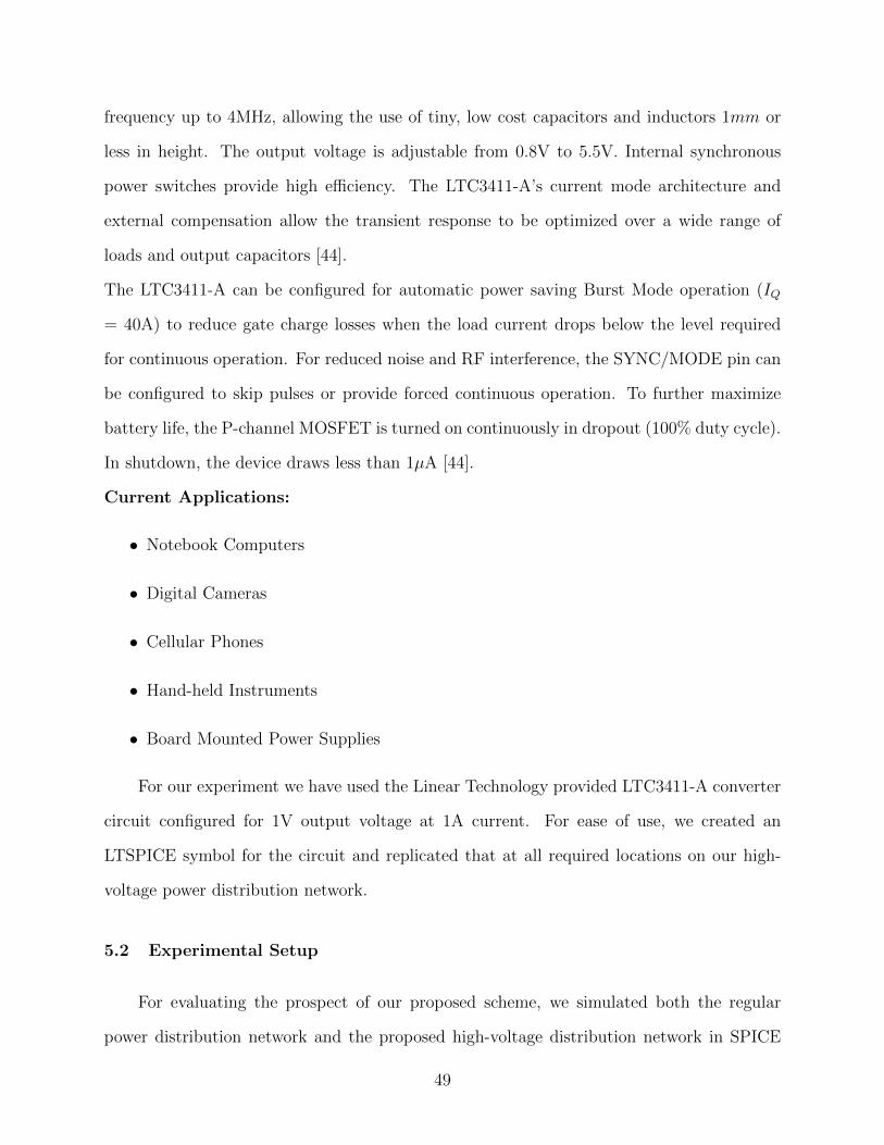
frequency up to 4MHz, allowing the use of tiny, low cost capacitors and inductors 1mm or
less in height. The output voltage is adjustable from 0.8V to 5.5V. Internal synchronous
power switches provide high efficiency. The LTC3411-A’s current mode architecture and
external compensation allow the transient response to be optimized over a wide range of
loads and output capacitors [44].
The LTC3411-A can be configured for automatic power saving Burst Mode operation (IQ
= 40A) to reduce gate charge losses when the load current drops below the level required
for continuous operation. For reduced noise and RF interference, the SYNC/MODE pin can
be configured to skip pulses or provide forced continuous operation. To further maximize
battery life, the P-channel MOSFET is turned on continuously in dropout (100% duty cycle).
In shutdown, the device draws less than 1µA [44].
Current Applications:
• Notebook Computers
• Digital Cameras
• Cellular Phones
• Hand-held Instruments
• Board Mounted Power Supplies
For our experiment we have used the Linear Technology provided LTC3411-A converter
circuit configured for 1V output voltage at 1A current. For ease of use, we created an
LTSPICE symbol for the circuit and replicated that at all required locations on our high-
voltage power distribution network.
5.2 Experimental Setup
For evaluating the prospect of our proposed scheme, we simulated both the regular
power distribution network and the proposed high-voltage distribution network in SPICE
49

and compared the results. We have simulated and comparatively analyzed the setup for
network sizes of 1, 4, 9, 16, 25, 64, 100 and 256 loads.
We have used LTSPICE, the SPICE simulator from Linear Technology, for all our sim-
ulations. We have assumed low power 1 watt loads, ideally running at 1V supply voltage
and drawing 1A current. We have modeled the loads as current sources. As for intercon-
nect resistances, we considered them to be 0.5Ω. We got this value consulting ITRS 2012
Datasheet [40]. We know that,
R = ρ · L
T ·W(5.1)
In our calculation, Interconnect resistivity, ρ = 2×10⁻⁶ Ω -cm
Interconnect thickness, T = 1×10⁻⁶ m
Interconnect width, W = 50×10−6 m
Interconnect length, L = 5×10⁻³ m
We have three cases in our experiment:
5.2.1 Present Day On-chip Power Distribution Network
In this case, power is delivered all over the circuit at 1V(Figure 5.1). We have simulated
this network for 1, 4, 9, 16, 25, 64, 100 and 256 load networks to evaluate and find power
consumption trend and efficiency of the design.
5.2.2 High-Voltage On-chip Power Distribution Network Considering Ideal DC-
DC Converters
Here, power is delivered all over the circuit at 3V. We have taken the value 3V as it
is very close to the supply voltage of a Lithium Ion battery operating at 90% efficiency.
Here, at each load point the DC-DC converter steps down the voltage to 1V and feeds it to
the loads (Figure 5.2). In this case, we assume the converters are ideal as in they are 100%
efficient and do not consume any power. We repeated the simulation for all the combinations
50
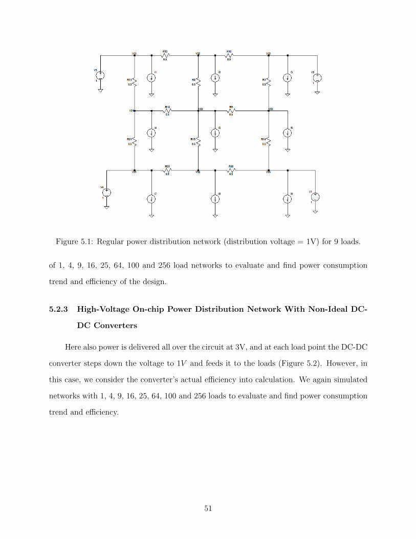
Figure 5.1: Regular power distribution network (distribution voltage = 1V) for 9 loads.
of 1, 4, 9, 16, 25, 64, 100 and 256 load networks to evaluate and find power consumption
trend and efficiency of the design.
5.2.3 High-Voltage On-chip Power Distribution Network With Non-Ideal DC-
DC Converters
Here also power is delivered all over the circuit at 3V, and at each load point the DC-DC
converter steps down the voltage to 1V and feeds it to the loads (Figure 5.2). However, in
this case, we consider the converter’s actual efficiency into calculation. We again simulated
networks with 1, 4, 9, 16, 25, 64, 100 and 256 loads to evaluate and find power consumption
trend and efficiency.
51
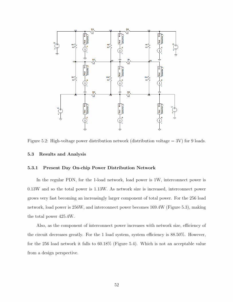
Figure 5.2: High-voltage power distribution network (distribution voltage = 3V) for 9 loads.
5.3 Results and Analysis
5.3.1 Present Day On-chip Power Distribution Network
In the regular PDN, for the 1-load network, load power is 1W, interconnect power is
0.13W and so the total power is 1.13W. As network size is increased, interconnect power
grows very fast becoming an increasingly larger component of total power. For the 256 load
network, load power is 256W, and interconnect power becomes 169.4W (Figure 5.3), making
the total power 425.4W.
Also, as the component of interconnect power increases with network size, efficiency of
the circuit decreases greatly. For the 1 load system, system efficiency is 88.50%. However,
for the 256 load network it falls to 60.18% (Figure 5.4). Which is not an acceptable value
from a design perspective.
52
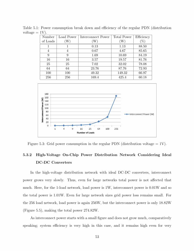
Table 5.1: Power consumption break down and efficiency of the regular PDN (distributionvoltage = 1V).
Number Load Power Interconnect Power Total Power Efficiencyof Loads (W) (W) (W) (%)
1 1 0.13 1.13 88.50
4 4 0.67 4.67 85.65
9 9 1.69 10.69 84.19
16 16 3.57 19.57 81.76
25 25 7.02 32.02 78.08
64 64 23.76 87.76 72.93
100 100 49.32 149.32 66.97
256 256 169.4 425.4 60.18
Figure 5.3: Grid power consumption in the regular PDN (distribution voltage = 1V).
5.3.2 High-Voltage On-Chip Power Distribution Network Considering Ideal
DC-DC Converters
In the high-voltage distribution network with ideal DC-DC converters, interconnect
power grows very slowly. Thus, even for large networks total power is not affected that
much. Here, for the 1-load network, load power is 1W, interconnect power is 0.01W and so
the total power is 1.01W. Even for large network sizes grid power loss remains small. For
the 256 load network, load power is again 256W, but the interconnect power is only 18.82W
(Figure 5.5), making the total power 274.82W.
As interconnect power starts with a small figure and does not grow much, comparatively
speaking; system efficiency is very high in this case, and it remains high even for very
53
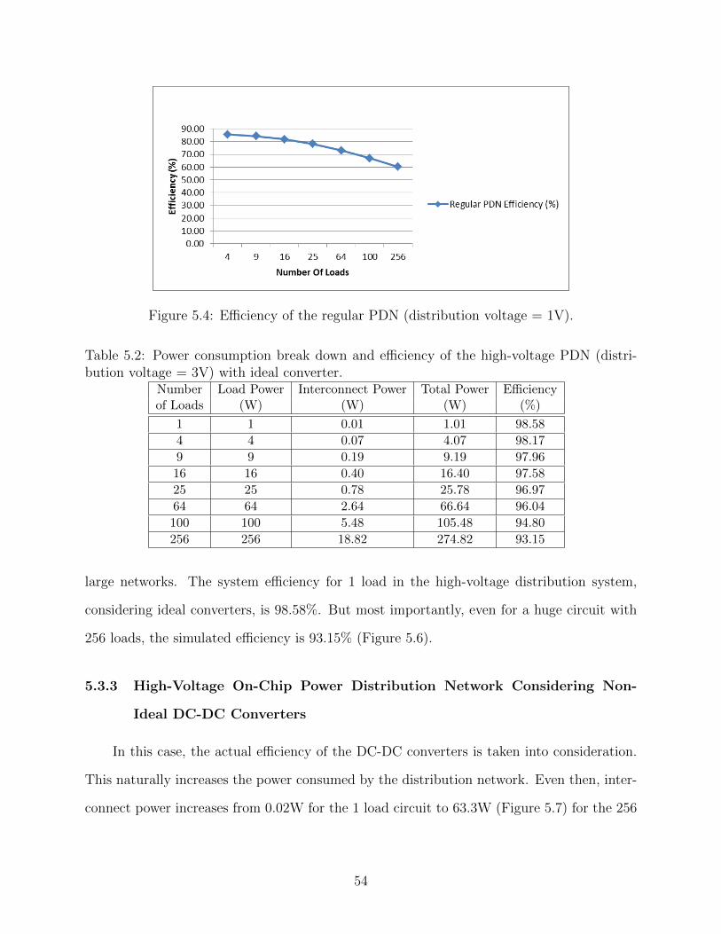
Figure 5.4: Efficiency of the regular PDN (distribution voltage = 1V).
Table 5.2: Power consumption break down and efficiency of the high-voltage PDN (distri-bution voltage = 3V) with ideal converter.
Number Load Power Interconnect Power Total Power Efficiencyof Loads (W) (W) (W) (%)
1 1 0.01 1.01 98.58
4 4 0.07 4.07 98.17
9 9 0.19 9.19 97.96
16 16 0.40 16.40 97.58
25 25 0.78 25.78 96.97
64 64 2.64 66.64 96.04
100 100 5.48 105.48 94.80
256 256 18.82 274.82 93.15
large networks. The system efficiency for 1 load in the high-voltage distribution system,
considering ideal converters, is 98.58%. But most importantly, even for a huge circuit with
256 loads, the simulated efficiency is 93.15% (Figure 5.6).
5.3.3 High-Voltage On-Chip Power Distribution Network Considering Non-
Ideal DC-DC Converters
In this case, the actual efficiency of the DC-DC converters is taken into consideration.
This naturally increases the power consumed by the distribution network. Even then, inter-
connect power increases from 0.02W for the 1 load circuit to 63.3W (Figure 5.7) for the 256
54

Figure 5.5: Grid power consumption in the high-voltage PDN (distribution voltage = 3V)with ideal converter.
Figure 5.6: Efficiency of the high-voltage PDN (distribution voltage = 3V) with ideal con-verter.
load circuit. This is an excellent result as it keeps total power consumed by the 256 load
circuit to a relatively low 319.3W.
A similar trend can be seen in the efficiency paradigm. In this case, system efficiency for
the 1 load network is 98.04%, and for the 256 load network it becomes 80.18% (Figure 5.8),
which is again an excellent performance for a such a huge circuit with readily available
technology.
55
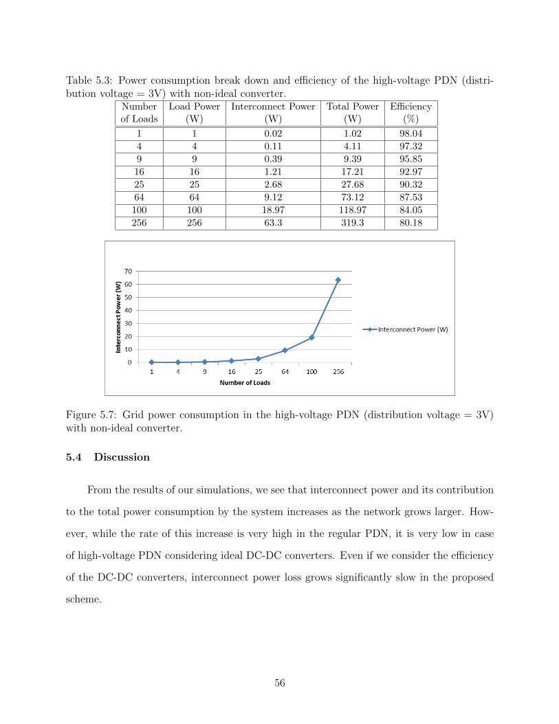
Table 5.3: Power consumption break down and efficiency of the high-voltage PDN (distri-bution voltage = 3V) with non-ideal converter.
Number Load Power Interconnect Power Total Power Efficiencyof Loads (W) (W) (W) (%)
1 1 0.02 1.02 98.04
4 4 0.11 4.11 97.32
9 9 0.39 9.39 95.85
16 16 1.21 17.21 92.97
25 25 2.68 27.68 90.32
64 64 9.12 73.12 87.53
100 100 18.97 118.97 84.05
256 256 63.3 319.3 80.18
Figure 5.7: Grid power consumption in the high-voltage PDN (distribution voltage = 3V)with non-ideal converter.
5.4 Discussion
From the results of our simulations, we see that interconnect power and its contribution
to the total power consumption by the system increases as the network grows larger. How-
ever, while the rate of this increase is very high in the regular PDN, it is very low in case
of high-voltage PDN considering ideal DC-DC converters. Even if we consider the efficiency
of the DC-DC converters, interconnect power loss grows significantly slow in the proposed
scheme.
56
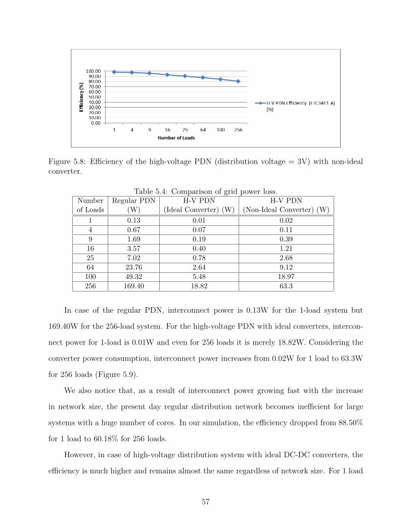
Figure 5.8: Efficiency of the high-voltage PDN (distribution voltage = 3V) with non-idealconverter.
Table 5.4: Comparison of grid power loss.Number Regular PDN H-V PDN H-V PDNof Loads (W) (Ideal Converter) (W) (Non-Ideal Converter) (W)
1 0.13 0.01 0.02
4 0.67 0.07 0.11
9 1.69 0.19 0.39
16 3.57 0.40 1.21
25 7.02 0.78 2.68
64 23.76 2.64 9.12
100 49.32 5.48 18.97
256 169.40 18.82 63.3
In case of the regular PDN, interconnect power is 0.13W for the 1-load system but
169.40W for the 256-load system. For the high-voltage PDN with ideal converters, intercon-
nect power for 1-load is 0.01W and even for 256 loads it is merely 18.82W. Considering the
converter power consumption, interconnect power increases from 0.02W for 1 load to 63.3W
for 256 loads (Figure 5.9).
We also notice that, as a result of interconnect power growing fast with the increase
in network size, the present day regular distribution network becomes inefficient for large
systems with a huge number of cores. In our simulation, the efficiency dropped from 88.50%
for 1 load to 60.18% for 256 loads.
However, in case of high-voltage distribution system with ideal DC-DC converters, the
efficiency is much higher and remains almost the same regardless of network size. For 1 load
57
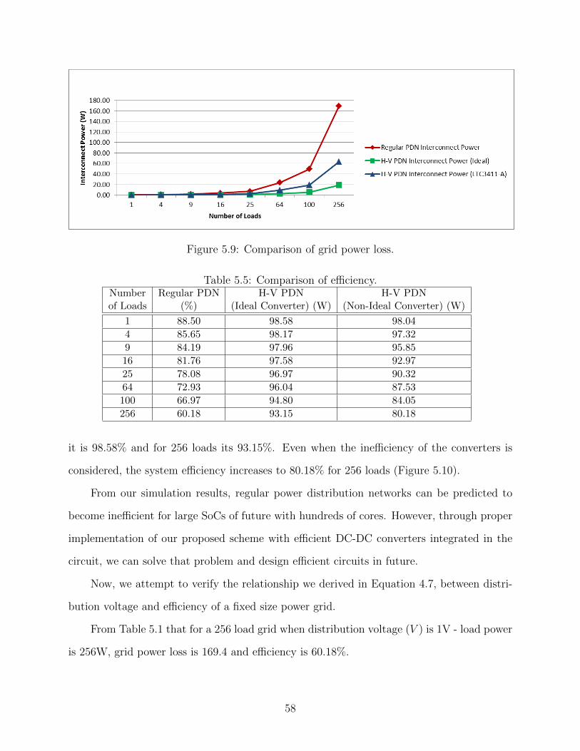
Figure 5.9: Comparison of grid power loss.
Table 5.5: Comparison of efficiency.Number Regular PDN H-V PDN H-V PDNof Loads (%) (Ideal Converter) (W) (Non-Ideal Converter) (W)
1 88.50 98.58 98.04
4 85.65 98.17 97.32
9 84.19 97.96 95.85
16 81.76 97.58 92.97
25 78.08 96.97 90.32
64 72.93 96.04 87.53
100 66.97 94.80 84.05
256 60.18 93.15 80.18
it is 98.58% and for 256 loads its 93.15%. Even when the inefficiency of the converters is
considered, the system efficiency increases to 80.18% for 256 loads (Figure 5.10).
From our simulation results, regular power distribution networks can be predicted to
become inefficient for large SoCs of future with hundreds of cores. However, through proper
implementation of our proposed scheme with efficient DC-DC converters integrated in the
circuit, we can solve that problem and design efficient circuits in future.
Now, we attempt to verify the relationship we derived in Equation 4.7, between distri-
bution voltage and efficiency of a fixed size power grid.
From Table 5.1 that for a 256 load grid when distribution voltage (V ) is 1V - load power
is 256W, grid power loss is 169.4 and efficiency is 60.18%.
58
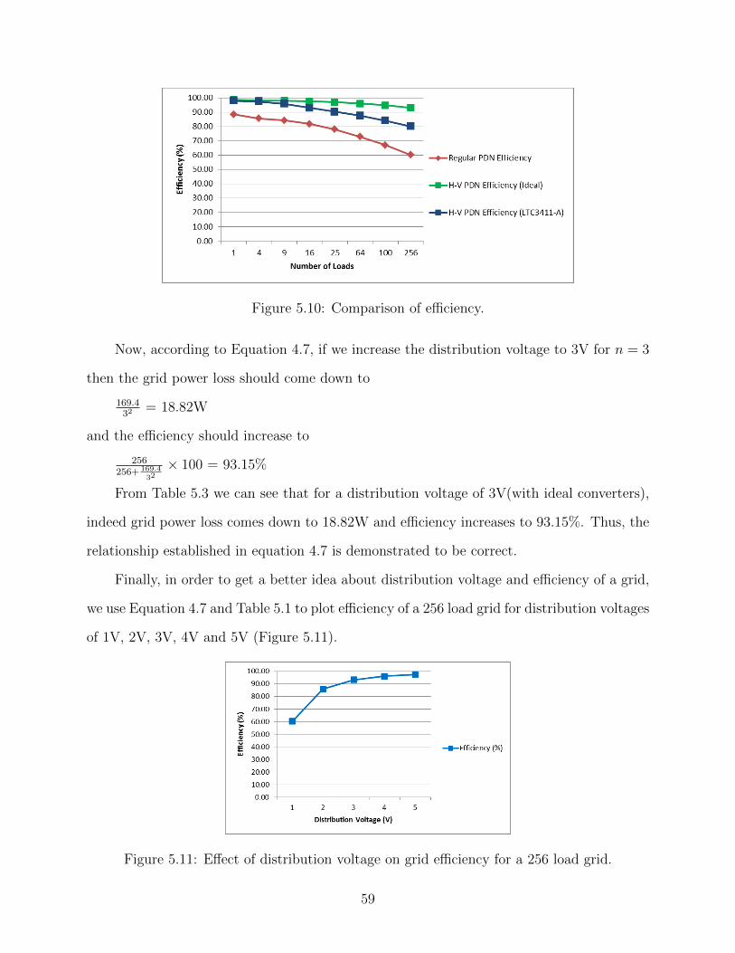
Figure 5.10: Comparison of efficiency.
Now, according to Equation 4.7, if we increase the distribution voltage to 3V for n = 3
then the grid power loss should come down to
169.432
= 18.82W
and the efficiency should increase to
256256+ 169.4
32× 100 = 93.15%
From Table 5.3 we can see that for a distribution voltage of 3V(with ideal converters),
indeed grid power loss comes down to 18.82W and efficiency increases to 93.15%. Thus, the
relationship established in equation 4.7 is demonstrated to be correct.
Finally, in order to get a better idea about distribution voltage and efficiency of a grid,
we use Equation 4.7 and Table 5.1 to plot efficiency of a 256 load grid for distribution voltages
of 1V, 2V, 3V, 4V and 5V (Figure 5.11).
Figure 5.11: Effect of distribution voltage on grid efficiency for a 256 load grid.
59

Chapter 6
Challenges, Developments and Future Work
From our simulation results we learned that, our proposed scheme is capable of suc-
cessfully solving the problem of designing highly efficient power distribution networks for
large chips with hundreds of cores. However, implementation of the scheme almost solely
depends on the development and availability of DC-DC converters with required efficiency.
This chapter discusses the challenges, recent developments and further work that need to
done in this regard.
6.1 Challenges
The decisive barrier that stands between the proposed scheme and reality is the challenge
of designing power and area efficient DC-DC converters that can be integrated on the chips.
The challenge is really three fold.
The first design challenge currently impeding the implementation of our scheme is the
efficiency of the DC-DC converters. It has to be efficient in both power and area. In the
proposed scheme, as the number of cores on the SoC goes up, so does the number of on-chip
DC-DC converters. Therefore, if the converters are not sufficiently power and area efficient,
they will unfortunately nullify the benefit of the scheme. At present, the converters capable
of supplying required amount of output current are often not that efficient.
Secondly, the converters need to be able to supply the output current and power drawn
by the load cores (micro-processors, GPU, etc.). Also they need to maintain the above
mentioned efficiency while driving such loads. Until now, DC-DC converter with sufficient
efficiency and large output drive are not available.
60
The final and main challenge in implementing the scheme is the fabrication of on-chip
DC-DC converters. It faces an imposing challenge because it requires on-chip integration of
inductive and capacitive devices for energy storage and output signal filtering. Integrated
capacitors and inductors beyond certain values are unacceptable due to the tight area con-
straints.
6.2 Recent Developments
At present, there exists no such DC-DC converter that fulfills all the aforementioned
requirements. However, technology is moving forward faster than ever, and what seemed
impossible just yesterday is already a reality today. In the last couple of years there have
been few spectacular developments in the area of on-chip DC-DC converters.
In [25], the authors describe a DC-DC converter, designed in 0.18 µm CMOS technology,
that has output voltage adjustable in the range of 1.3V - 1.6V from the input voltage of 3.3V.
The output current driving capability of the converter is up to 26 mA. They report power
efficiency for the unregulated and regulated output to be 87% and 75%, respectively.
Authors of [23] also reported two designs for high-to-low DC-DC converters integrated
onto the same die as a high performance microprocessor. The first design performs a voltage
conversion from 3.6V to 0.9V, while supplying 250mA of current, with an efficiency of 87.8%.
The second design demonstrated an efficiency of 79.6% for a voltage conversion from 5.4V
to 0.9V while supplying 250mA of DC current.
6.3 Future Work
While the experimental simulations in this work have demonstrated the potential of the
proposed high-voltage power distribution scheme, our work is far from over. Much work
needs to be put in, especially to overcome the challenges of design and fabrication of efficient
on-chip DC-DC converters, to make the proposal a reality. We need to work on developing
DC-DC converters that meets the following general guidelines:
61

• Have the capability of driving output loads of reasonable size (e.g., 1W).
• Have power efficiency of 90% or higher.
• Be small enough to meet the tight area requirements modern high-density ICs.
• Can be fabricated on-chip as a part of the SoC.
Though the recent developments mentioned earlier, do not quite meet all of these re-
quirements, they definitely make us hopeful and give the direction to go forward.
62
Chapter 7
Conclusion
As performance oriented portable computing devices and power aware high-performance
computers have set themselves as the future the VLSI industry, optimizing between power
and performance has become absolutely essential. In this thesis, we have first discussed power
consumption in CMOS circuits, and the measures taken to resolve this challenge. Then we
have analyzed the present day on-chip Power Distribution Network (PDN). We have seen
that, though the existing distribution network designs take into consideration issues like
IR drop and crosstalk noise, they practically ignore the power loss in the network. We
have proposed a novel scheme of high-voltage power delivery, which holds great promise for
designing high efficiency on-chip power distribution networks. In the new scheme we propose
delivering power to different modules/cores on a System-on-Chip (SoC), at a higher voltage
and lower current, and thereby reduce the I2R loss in the on-chip power distribution network.
We have demonstrated our claim of power saving by simulating representative circuit models
of regular and proposed distribution networks in SPICE, and comparing the results. The
SPICE simulations show that, for a 256 load network, when distributed at 3V (a voltage
close to the nominal output of a Li-ion battery), and then down-converted to VDD of 1V,
instead of distributing at 1V , the efficiency of the circuit can go up from a mere 60% to more
than a staggering 90%. The proposed scheme actually showed incremental power saving as
the complexity of the SoC went up. The scheme, because of its high-voltage feature, is
also expected to diminish other issues like IR drop, electromigration, and cross-talk in the
distribution network. Though the potential of this scheme for power reduction was validated
by this work, its development is far from over. We need to work on to resolve the fabrication
challenges, and on designing efficient on-chip DC-DC converters. However, expecting viable
63

implementation of required on-chip DC-DC converters in near future, this scheme can reduce
losses in the power grid to the level required for designing thousand core processors in future.
64
Bibliography
[1] “American Electric Power Transmission Facts .” http://bit.ly/11nUMvf; accessed on July 01,2013.
[2] “Ball Grid Array Packaging.” http://www.techfuels.com/processors/1509-ball-grid-array.html; accessed on Mayl 28, 2013.
[3] “Computer History Timeline.” http://www.computerhistory.org/semiconductor/timeline.html;accessed on July 09, 2013.
[4] “Designing With High-Density BGA Packages for Altera Devices.” http://www.altera.com/literature/an/an114.pdf; accessed on Mayl 28, 2013.
[5] “Electric Power Transmission.” [http://bit.ly/15ar90; accessed on July 01,2013].
[6] “Linear Technology.” http://en.wikipedia.org/wiki/Linear Technology; accessed on April 17,2013.
[7] “Linear Technology Corporation.” http://www.linear.com/company/; accessed on April 17,2013.
[8] “Semiconductor Device-and-Lead Architecture.” http://bit.ly/178vY00; accessed on July 09,2013.
[9] “Semiconductor Equipment and Materials Industry Timeline.” http://bit.ly/14mUIz1; ac-cessed on July 09, 2013.
[10] “The Central Processing Unit (CPU).” http://www.techfuels.com/processors/1509-ball-grid-array.html; accessed on Mayl 28, 2013.
[11] “The Theory of p-n Junctions and p-n Junction Transistors.” http://bit.ly/17yWtPE; accessedon July 09, 2013.
[12] M. Aguareles, J. Blasco, M. Pellicer, and J. Sola-Morales, “Voltage Drop in On-Chip PowerDistribution Networks,” Grups dEstudi de Matematica i Tecnologia, Centre de Recerca Matem-atica, Bellaterra, Barcelona, Spain, pp. 45–60, 2009.
[13] A. H. Ajami, K. Banerjee, and M. Pedram, “Scaling Analysis of On-Chip Power Grid Volt-age Variations in Nanometer Scale ULSI,” Analog Integrated Circuits and Signal Processing,vol. 42, no. 3, pp. 277–290, 2005.
[14] K. Arabi, R. Saleh, and M. Xiongfei, “Power Supply Noise in SoCs: Metrics, Management,and Measurement,” IEEE Design & Test of Computers, vol. 24, no. 3, pp. 236–244, 2007.
[15] T.-H. Chen and C. C.-P. Chen, “Efficient Large-Scale Power Grid Analysis Based on Pre-conditioned Krylov-Subspace Iterative Methods,” in Proceedings of IEEE Design AutomationConference, 2001, pp. 559–562.
65

[16] D. Chinnery and K. Keutzer, Closing the Power Gap Between ASIC and Custom: Tools andTechniques for Low Power Design. Springer, 2007.
[17] R. W. Erickson, DCDC Power Converters. John Wiley and Sons, Inc., 2001.
[18] J. Fu, Z. Luo, X. Hong, Y. Cai, Z. Pan, and S.-D. Tan, “VLSI On-Chip Power/Ground NetworkOptimization Considering Decap Leakage Currents,” in Proceedings of IEEE Asia and SouthPacific Design Automation Conference, volume 2, 2005, pp. 735–738.
[19] M. S. Gupta, J. L. Oatley, R. Joseph, G.-Y. Wei, and D. M. Brooks, “Understanding VoltageVariations in Chip Multiprocessors using a Distributed Power-Delivery Network,” in Proceed-ings of IEEE Design, Automation & Test in Europe Conference & Exhibition, 2007, pp. 1–6.
[20] R. Jakushokas, Power Distribution Networks with OnChip Decoupling Capacitors. Springer,2011.
[21] M. Keating, D. Flynn, R. Aitken, A. Gibbons, and K. Shi, Low Power Methodology Manualfor SystemonChip design. Springer, 2007.
[22] P. Khem, “Physical and Silicon Measures of Low Power Clock Gating Success: An Apple toApple Case Study,” in Proceedings of the 11th International Symposium on High-PerformanceComputer Architecture, SNUG, 2007.
[23] V. Kursun and E. G. Friedman, MultiVoltage CMOS Circuit Design. Wiley, 2006.
[24] C. Loh, K. Toh, D. Pinjala, and M. Iyer, “Development of Effective Compact Models forDepopulated Ball Grid Array Packages,” in Proceedings of IEEE Electronics Packaging Tech-nology Conference, 2000, pp. 131–137.
[25] B. Maity, S. Gangula, and P. Mandal, “Design and Implementation of an Area and Power Ef-ficient SwitchedCapacitor Based Embedded DC-DC Converter,” Journal of Low Power Elec-tronics, vol. 8, no. 2, pp. 207–222, 2012.
[26] G. E. Moore, “Cramming More Components onto Integrated Circuits,” Electronics, vol. 38,no. 8, Apr. 1965.
[27] G. E. Moore, “Progress in Digital Integrated Electronics,” in IEEE International ElectronDevices Meeting Digest, 1975, pp. 11–13.
[28] G. E. Moore, “Lithography and the Future of Moore’s Law,” Proc. SPIE, vol. 2437, May 1995.
[29] S. Narendra, S. Borkar, V. De, D. Antoniadis, and A. Chandrakasan, “Scaling of Stack Ef-fect and Its Application for Leakage Reduction,” in International Symposium on Low PowerElectronics and Design, 2001, pp. 195–200.
[30] S. R. Nassif, “Power Grid Analysis Benchmarks,” in Proceedings of IEEE Asia and SouthPacific Design Automation Conference, 2008, pp. 376–381.
[31] C. Neau and K. Roy, “Optimal Body Bias Selection for Leakage Improvement and ProcessCompensation over Different Technology Generations,” in Proceedings of the InternationalSymposium on Low Power Electronics and Design, (New York, NY, USA), 2003, pp. 116–121.
[32] S. Ouimet, J. Casey, K. Marston, J. Muncy, J. Corbin, V. Jadhav, T. Wassick, and I. Depatie,“Development of a 50mm Dual Flip Chip Plastic Land Grid Array Package for Server Appli-cations,” in IEEE Electronic Components and Technology Conference, 2008, pp. 1900–1906.
66
[33] R. Panda, D. Blaauw, R. Chaudhry, V. Zolotov, B. Young, and R. Ramaraju, “Model andAnalysis for Combined Package and On-Chip Power Grid Simulation,” in Proceedings of IEEEInternational Symposium onLow Power Electronics and Design, 2000, pp. 179–184.
[34] S. Pant, Design and Analysis of Power Distribution Networks in VLSI Circuits. ProQuest,2008.
[35] S. Park, J. Park, D. Shin, Y. Wang, Q. Xie, M. Pedram, and N. Chang, “Accurate Modelingof the Delay and Energy Overhead of Dynamic Voltage and Frequency Scaling in ModernMicroprocessors,” 2012.
[36] B. C. Paul, A. Agarwal, and K. Roy, “Low-Power Design Techniques for Scaled Technologies,”Integration, the VLSI Journal, vol. 39, no. 2, pp. 64 – 89, 2006.
[37] M. Pedram and J. M. Rabaey, Power Aware Design Methodologies. Springer, 2002.
[38] M. Popovich, E. G. Friedman, M. Sotman, and A. Kolodny, “On-Chip Power DistributionGrids with Multiple Supply Voltages for High-Performance Integrated Circuits,” IEEE Trans-actions on Very Large Scale Integration (VLSI) Systems, vol. 16, no. 7, pp. 908–921, 2008.
[39] R. Schaller, “Moore’s Law: Past, Present and Future,” IEEE Spectrum, vol. 34, no. 6, pp.52–59, 1997.
[40] Semiconductor Industry Association, “International Technology Roadmap for Semiconduc-tors,” 2012. http://www.itrs.net/Links/2012ITRS/Home2012.htm.
[41] K. Shah, “Power Grid Analysis In VLSI Designs,” 2009.
[42] D. Stringfellow and J. Pedicone, “Decoupling Capacitance Estimation, Implementation, andVerification: A Practical Approach for Deep Submicron SoCs,” Synopsys Users Group, 2007.
[43] P. Sun, X. Li, and M.-Y. Ting, “Efficient Incremental Analysis of On-Chip Power Grid ViaSparse Approximation,” in Proceedings 48th ACM Design Automation Conference, 2011, pp.676–681.
[44] L. Technology, “Linear Technology: LT3411A DC-DC Converter Demo Circuit @ONLINE,”Nov. 2011.
[45] A. von Meier, Electric Power Systems: A Conceptual Introduction.
[46] N. H. E. Weste and D. Harris, CMOS VLSI design: A Circuits and Systems Perspective.Pearson, 2006.
[47] K. S. Yeo and K. Roy, Low Voltage, Low Power VLSI Subsystems.
[48] Q. K. Zhu, Power Distribution Network Design for VLSI. Wiley, 2004.
67