Embed Size (px)
Citation preview
A High-Resolution Combined Scanning Laser- and Widefield PolarizingMicroscope for Imaging at Temperatures from 4 K to 300 K
M. Lange,1 S. Guenon,1 F. Lever,1 R. Kleiner,1 and D. Koelle1
Physikalisches Institut - Experimentalphysik II and Center for Quantum Science (CQ) in LISA+,Universitat Tubingen, D-72076 Tubingen, Germany
(Dated: 17 November 2017)
Polarized light microscopy, as a contrast-enhancing technique for optically anisotropic mate-rials, is a method well suited for the investigation of a wide variety of effects in solid-statephysics, as for example birefringence in crystals or the magneto-optical Kerr effect (MOKE).We present a microscopy setup that combines a widefield microscope and a confocal scanninglaser microscope with polarization-sensitive detectors. By using a high numerical apertureobjective, a spatial resolution of about 240 nm at a wavelength of 405 nm is achieved. Thesample is mounted on a 4He continuous flow cryostat providing a temperature range between4 K and 300 K, and electromagnets are used to apply magnetic fields of up to 800 mT withvariable in-plane orientation and 20 mT with out-of-plane orientation. Typical applicationsof the polarizing microscope are the imaging of the in-plane and out-of-plane magnetizationvia the longitudinal and polar MOKE, imaging of magnetic flux structures in superconduc-tors covered with a magneto-optical indicator film via Faraday effect or imaging of structuralfeatures, such as twin-walls in tetragonal SrTiO3. The scanning laser microscope furthermoreoffers the possibility to gain local information on electric transport properties of a sample bydetecting the beam-induced voltage change across a current-biased sample. This combinationof magnetic, structural and electric imaging capabilities makes the microscope a viable toolfor research in the fields of oxide electronics, spintronics, magnetism and superconductivity.
I. INTRODUCTION
The properties of ferroic materials and devices arestrongly affected by their microscopic domain structure.Knowledge about the domains often plays a key role inthe understanding and interpretation of integral mea-surements, which puts an emphasis on the importanceof imaging techniques. Polarized light microscopy isan excellent tool for this purpose and has been suc-cessfully applied to ferromagnetic1, ferroelastic2 and fer-roelectric3,4 domain imaging. Alternative methods forimaging of magnetic domains include Bitter decoration5,Lorentz microscopy6, electron holography7, magneticforce microscopy8, scanning SQUID microscopy9, scan-ning Hall probe microscopy10, nitrogen vacancy centermicroscopy11, X-ray magnetic circular dichroism12, scan-ning electron microscopy (SEM)13, and SEM with polar-ization analysis (SEMPA)14. A comparison of most ofthese methods can be found in Ref.15. Imaging of fer-roelectric domains has also been accomplished by etch-ing16, nanoparticle decoration17, scanning electron mi-croscopy18, piezoresponse force microscopy19 and X-raydiffraction20. These techniques have been reviewed byPotnis et al.21 and by Soergel22.
Polarized light imaging provides a non-destructive,non-contact way to observe ferroic domains with sub-µm resolution and high sensitivity that can be carriedout in high magnetic fields. The contrast for imaging offerroelastic or ferroelectric domains arises from birefrin-gence or bireflectance23,24, which is a consequence of theanisotropic permittivity tensor of these materials. Ferro-magnetic domains, on the other hand, can be imaged viathe magneto-optical Kerr effect25 (MOKE) or the Fara-day effect26. Both confocal laser scanning 27 and wide-field28 microscopy can be used for imaging with polarized
light contrast. In confocal laser scanning microscopy theimage is captured sequentially by scanning a focussedlaser beam across the sample. A confocal pinhole elim-inates light that does not originate from the focal vol-ume. This results in a high depth discrimination, con-trast enhancement and a 28 % increase in lateral resolu-tion. Widefield microscopy, on the other hand, has theadvantage of faster acquisition rates and simultaneousimage formation.
The instrument discussed below is based on an ear-lier design by Guenon29 and combines a widefield- anda confocal laser scanning microscope with polarization-sensitive detectors. To study effects at low temperaturesand in magnetic fields, the sample is mounted on a liquid-helium continuous flow cryostat offering a temperaturerange of 4 K to 300 K and magnetic fields up to 800 mTwith variable orientation can be applied. The confocallaser scanning microscope offers an additional imagingmechanism: a beam-induced voltage across a current-biased sample can be generated by the local perturba-tion of the laser beam. This beam-induced voltage canbe used to extract local information on the electric trans-port properties of the sample30–34. While several exam-ples of low-temperature widefield35–37 and laser scanningpolarizing microscopes38–40 have been published, the in-strument presented here stands out with regard to theversatility offered by combining widefield and confocallaser scanning imaging modes, the accessible tempera-ture range, as well as the very high lateral resolution itprovides at low temperatures.
This paper is organized as follows. Given the rele-vance for the design of the microscope, a brief overviewof MOKE and Faraday effect is given in Section II. Thecryostat and the generation of magnetic fields is describedin Section III. The widefield polarizing microscope is
arX
iv:1
711.
0620
4v1
[ph
ysic
s.in
s-de
t] 1
5 N
ov 2
017
2
discussed in Section IV and a detailed description ofthe scanning laser microscope is presented in Section V.Imaging of electric transport properties is addressed inSection VI and examples demonstrating the performanceof the instrument are presented in Section VII.
II. MAGNETO-OPTICAL KERR EFFECT (MOKE) ANDFARADAY EFFECT
The observation of domains in magnetic materials re-lies mainly on two magneto-optical effects: the magneto-optical Kerr effect (MOKE) in reflection and the Faradayeffect in transmission. Both effects lead to a rotation ofthe plane of polarization that depends linearly on magne-tization and is caused by different refractive indices forleft-handed and right-handed circularly polarized light(magnetic circular birefringence).
A distinction between three types of MOKE with re-gard to the orientation of the magnetization and theplane of incidence is made: polar, longitudinal and trans-verse MOKE, being sensitive to the out-of-plane magne-tization component, the in-plane magnetization compo-nent along the plane of incidence and the in-plane mag-netization component perpendicular to the plane of inci-dence, respectively. For linearly polarized light, both thelongitudinal and the polar MOKE lead to a rotation ofthe plane of polarization upon reflection on the samplesurface, while the transverse MOKE leads to a modula-tion of the reflected intensity. In addition to the rotationof the plane of polarization the longitudinal and polarMOKE also lead to elliptically polarized light caused bya difference in absorption for left- and right-handed cir-cularly polarized light. Furthermore, the MOKE also de-pends on the angle of incidence (AOI). The polar MOKEis an even function of AOI and has the largest amplitudefor normal incidence. The longitudinal MOKE is an oddfunction of AOI and increases with increasing AOI.
The Faraday effect can be observed when light is trans-mitted through transparent ferromagnetic or paramag-netic materials. It describes a rotation of the plane ofpolarization that is proportional to the magnetizationcomponent along the propagation direction of the lightand the length of the path on which the light interactswith the material. An important application of the Fara-day effect are magneto-optical indicator films41 (MOIF),that can be used to image the stray field above a sam-ple. These typically consist of a thin garnet film with in-plane anisotropy that is coated with a mirror on one side.The mirror side of the MOIF is placed in direct contactwith the sample under investigation and observed underperpendicular illumination with a polarizing microscope.The stray field of the sample leads to a deflection of themagnetization in the MOIF, that now has a componentalong the propagation direction of the light and thus be-comes observable via the Faraday effect.
Additional magneto-optical effects that are rarely usedfor domain imaging are the Voigt effect and the Cotton-Mouton effect. A detailed description of the variousmagneto-optical effects can be found in Ref. 1 and 15.
III. CRYOSTAT, ELECTROMAGNET
The cryostat and microscope are mounted on a vibra-tionally isolated optical table. Since the sample is fixedon a coldfinger, the microscope needs to be positionedrelative to the sample with sub-µm resolution. A verysturdy, yet precise, positioning unit needs to be used.The microscope is connected to the cryostat via flexiblebellows to allow for the positioning of the microscope.The cryostat is a liquid-helium continuous flow cryostatwith the sample in vacuum. The temperature can be ad-justed in a range of T = 4 K to T = 300 K. The coldfingerand sample holder have a diameter of 25.4 mm. Electri-cal contacts and mounting screws around the perime-ter of the sample holder limit the available space forsample mounting. Samples with a dimension of up to12 mm× 12 mm can be conveniently mounted.
Two electromagnets are used to generate in-plane mag-netic fields of up to B‖ = ±800 mT and out-of-planemagnetic fields of up to B⊥ = ±20 mT. The electromag-nets are mounted on a frame that is separated from therest of the setup to reduce the risk of vibrations beingtransferred to the microscope. The out-of-plane mag-netic field is generated by a Helmholtz coil that achievesa field homogeneity of 0.2 % in a cylindrical volume of5 mm length in out-of-plane direction and 20 mm diam-eter in the sample plane. The magnet, generating thein-plane magnetic field, can be rotated around the cryo-stat to allow for an adjustment of the orientation of thein-plane magnetic field. The in-plane magnetic field is ho-mogeneous to within 1 % in a cubic volume with an edgelength of 12 mm. The magnetic fields for both magnetshave been calibrated using a Hall probe with an accuracyof 2 %. Due to spatial constraints limiting the size of theHelmholtz coil, the achievable out-of-plane magnetic fieldstrength is limited to 20 mT. The range of applications ofthe instrument could be enhanced by replacing the twoelectromagnets by a superconducting vector magnet thatallows the application of magnetic fields with a strength> 1 T and variable orientation.
IV. LOW-TEMPERATURE WIDEFIELD POLARIZINGMICROSCOPE (LTWPM)
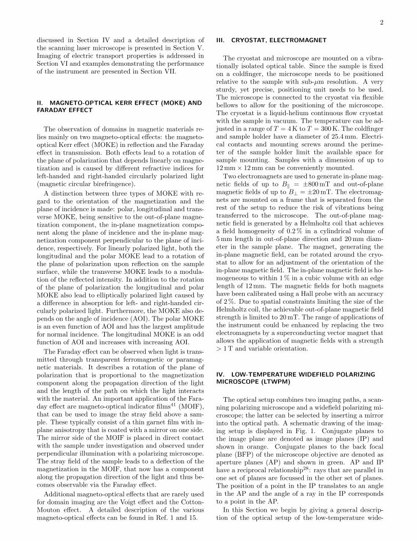
The optical setup combines two imaging paths, a scan-ning polarizing microscope and a widefield polarizing mi-croscope; the latter can be selected by inserting a mirrorinto the optical path. A schematic drawing of the imag-ing setup is displayed in Fig. 1. Conjugate planes tothe image plane are denoted as image planes (IP) andshown in orange. Conjugate planes to the back focalplane (BFP) of the microscope objective are denoted asaperture planes (AP) and shown in green. AP and IPhave a reciprocal relationship28: rays that are parallel inone set of planes are focussed in the other set of planes.The position of a point in the IP translates to an anglein the AP and the angle of a ray in the IP correspondsto a point in the AP.
In this Section we begin by giving a general descrip-tion of the optical setup of the low-temperature wide-
3
FIG. 1. Schematic overview of the optical setup. Conjugate image planes (IP) are displayed in orange, conjugate apertureplanes (AP) in green. The setup combines two imaging paths that can be selected via the removable mirror. A widefieldpolarizing microscope (mirror inserted), in which the sample is imaged onto the sensor of the camera, and a scanning polarizingmicroscope (mirror removed), that uses a fast-steering mirror (FSM) to scan a laser-beam across the sample.
field polarizing microscope (LTWPM) before we proceedwith a detailed description of the components and theirfunction. The LTWPM can be used by inserting the re-movable mirror, as indicated by the broken lines in theray diagram (Fig. 1). The illumination follows a Koehlerscheme42 and the sample is illuminated through the mi-croscope objective. The light source for the LTWPMis realized by fiber-coupled light-emitting diodes (LED),that are combined into a fiber bundle. The fiber bun-dle end face is imaged into the back focal plane of the
microscope objective. To achieve this, the fiber outputis collimated (collimator-2) and the field lens is used toimage the fiber ends into an AP at the position of aninterchangeable aperture stop (aperture stop-2). A ro-tatable polarizer in front of the aperture stop is used todefine the plane of polarization. A field stop, alignedwith the shared focal plane of collimator-2 and the fieldlens, can be used to confine the illuminated sample area.After passing a polarization maintaining beam splitter(PMBS-2), the light is reflected by the removable mirror
4
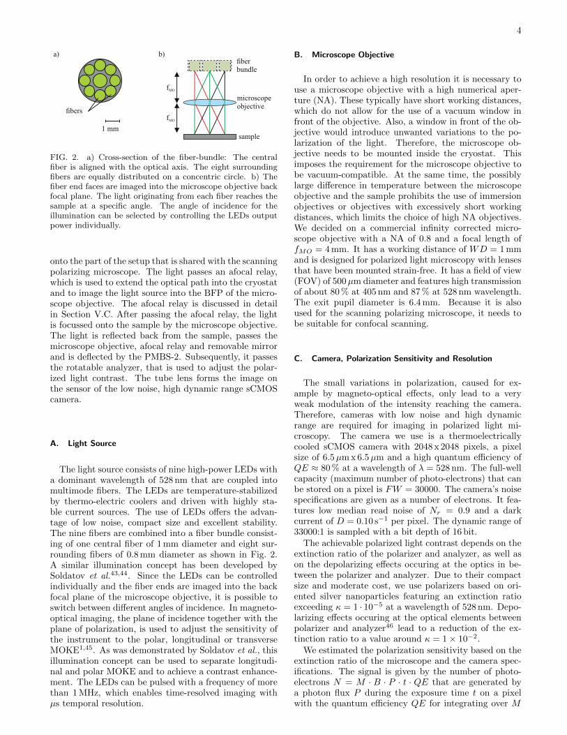
FIG. 2. a) Cross-section of the fiber-bundle: The centralfiber is aligned with the optical axis. The eight surroundingfibers are equally distributed on a concentric circle. b) Thefiber end faces are imaged into the microscope objective backfocal plane. The light originating from each fiber reaches thesample at a specific angle. The angle of incidence for theillumination can be selected by controlling the LEDs outputpower individually.
onto the part of the setup that is shared with the scanningpolarizing microscope. The light passes an afocal relay,which is used to extend the optical path into the cryostatand to image the light source into the BFP of the micro-scope objective. The afocal relay is discussed in detailin Section V.C. After passing the afocal relay, the lightis focussed onto the sample by the microscope objective.The light is reflected back from the sample, passes themicroscope objective, afocal relay and removable mirrorand is deflected by the PMBS-2. Subsequently, it passesthe rotatable analyzer, that is used to adjust the polar-ized light contrast. The tube lens forms the image onthe sensor of the low noise, high dynamic range sCMOScamera.
A. Light Source
The light source consists of nine high-power LEDs witha dominant wavelength of 528 nm that are coupled intomultimode fibers. The LEDs are temperature-stabilizedby thermo-electric coolers and driven with highly sta-ble current sources. The use of LEDs offers the advan-tage of low noise, compact size and excellent stability.The nine fibers are combined into a fiber bundle consist-ing of one central fiber of 1 mm diameter and eight sur-rounding fibers of 0.8 mm diameter as shown in Fig. 2.A similar illumination concept has been developed bySoldatov et al.43,44. Since the LEDs can be controlledindividually and the fiber ends are imaged into the backfocal plane of the microscope objective, it is possible toswitch between different angles of incidence. In magneto-optical imaging, the plane of incidence together with theplane of polarization, is used to adjust the sensitivity ofthe instrument to the polar, longitudinal or transverseMOKE1,45. As was demonstrated by Soldatov et al., thisillumination concept can be used to separate longitudi-nal and polar MOKE and to achieve a contrast enhance-ment. The LEDs can be pulsed with a frequency of morethan 1 MHz, which enables time-resolved imaging withµs temporal resolution.
B. Microscope Objective
In order to achieve a high resolution it is necessary touse a microscope objective with a high numerical aper-ture (NA). These typically have short working distances,which do not allow for the use of a vacuum window infront of the objective. Also, a window in front of the ob-jective would introduce unwanted variations to the po-larization of the light. Therefore, the microscope ob-jective needs to be mounted inside the cryostat. Thisimposes the requirement for the microscope objective tobe vacuum-compatible. At the same time, the possiblylarge difference in temperature between the microscopeobjective and the sample prohibits the use of immersionobjectives or objectives with excessively short workingdistances, which limits the choice of high NA objectives.We decided on a commercial infinity corrected micro-scope objective with a NA of 0.8 and a focal length offMO = 4 mm. It has a working distance of WD = 1 mmand is designed for polarized light microscopy with lensesthat have been mounted strain-free. It has a field of view(FOV) of 500µm diameter and features high transmissionof about 80 % at 405 nm and 87 % at 528 nm wavelength.The exit pupil diameter is 6.4 mm. Because it is alsoused for the scanning polarizing microscope, it needs tobe suitable for confocal scanning.
C. Camera, Polarization Sensitivity and Resolution
The small variations in polarization, caused for ex-ample by magneto-optical effects, only lead to a veryweak modulation of the intensity reaching the camera.Therefore, cameras with low noise and high dynamicrange are required for imaging in polarized light mi-croscopy. The camera we use is a thermoelectricallycooled sCMOS camera with 2048 x 2048 pixels, a pixelsize of 6.5µm x 6.5µm and a high quantum efficiency ofQE ≈ 80 % at a wavelength of λ = 528 nm. The full-wellcapacity (maximum number of photo-electrons) that canbe stored on a pixel is FW = 30000. The camera’s noisespecifications are given as a number of electrons. It fea-tures low median read noise of Nr = 0.9 and a darkcurrent of D = 0.10 s−1 per pixel. The dynamic range of33000:1 is sampled with a bit depth of 16 bit.
The achievable polarized light contrast depends on theextinction ratio of the polarizer and analyzer, as well ason the depolarizing effects occuring at the optics in be-tween the polarizer and analyzer. Due to their compactsize and moderate cost, we use polarizers based on ori-ented silver nanoparticles featuring an extinction ratioexceeding κ = 1 · 10−5 at a wavelength of 528 nm. Depo-larizing effects occuring at the optical elements betweenpolarizer and analyzer46 lead to a reduction of the ex-tinction ratio to a value around κ = 1× 10⁻².
We estimated the polarization sensitivity based on theextinction ratio of the microscope and the camera spec-ifications. The signal is given by the number of photo-electrons N = M · B · P · t · QE that are generated bya photon flux P during the exposure time t on a pixelwith the quantum efficiency QE for integrating over M
5
0 10 20 30 40 50 60
analyzer angle β [◦]
0
1
2
3
4
5
6
7θmin·
√
M·B[rad
]×10
-3
1
1.2
1.4
1.6
1.8
2
sensitivity[rad
/√
Hz]
×10-4
detection limit
sensitivity
FIG. 3. Detection limit θmin
√M ·B (solid blue line) and
sensitivity (dashed red line) as a function of analyzer angle.
exposures and binning of B pixels. The noise sourcescontributing to the overall noise are: The signal relatedshot noise δshot =
√N , dark noise δdark =
√M ·B ·D · t
due to thermally generated electrons and readout noiseδread =
√M ·B ·Nr. By adding the noise contributions
in quadrature we derive the signal-to-noise ratio
SNR =√M ·B · P · t ·QE√
P · t ·QE +D · t+N2r
. (1)
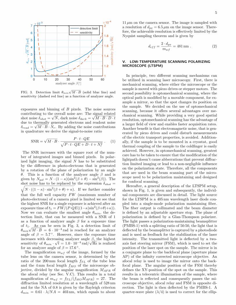
The SNR increases with the square root of the num-ber of integrated images and binned pixels. In polar-ized light imaging, the signal N has to be substitutedby the difference in photo-electrons that is generatedby a rotation of the plane of polarization by an angleθ. This is a function of the analyzer angle β and isgiven by Npol = N · (1 − κ)(sin2(β + θ) − sin2(β)). Theshot noise has to be replaced by the expression δshot =√N · ((1− κ) · sin2(β + θ) + κ). If we further consider
that the full well capacity FW (maximum number ofphoto-electrons) of a camera pixel is limited we see thatthe highest SNR for a single exposure is achieved after anexposure time of t1 = FW/(P ·QE((1−κ)sin2(β+θ)+κ)).Now we can evaluate the smallest angle θmin, the de-tection limit, that can be measured with a SNR of 1as a function of analyzer angle β for a exposure timeof t1. As can be seen in Fig. 3, a detection limit ofθmin
√M ·B = 6 · 10−4 rad is reached for an analyzer
angle of β = 5.7 ◦. However, since the exposure timeincreases with decreasing analyzer angle β, the highestsensitivity of θmin ·
√t = 1.0 · 10−4 rad/
√Hz is realized
for an analyzer angle of β = 17.6 ◦.The magnification mwf of the image, formed by the
tube lens on the camera sensor, is determined by theratio of the 200 mm focal length fTL of the tube lensand the 4 mm focal length fMO of the microscope ob-jective, divided by the angular magnification MAFR ofthe afocal relay (see Sec. V.C). This results in a totalmagnification of mwf = fTL/(fMOMAFR) = 27. Thediffraction limited resolution at a wavelength of 528 nmand for the NA of 0.8 is given by the Rayleigh criteriondmin = 0.61 · λ/NA = 403 nm, which equals to about
11µm on the camera sensor. The image is sampled witha resolution of dpx = 6.5µm on the image sensor. There-fore, the achievable resolution is effectively limited by theNyquist sampling theorem and is given by
deff =2 · dpxmwf
= 481 nm . (2)
V. LOW-TEMPERATURE SCANNING POLARIZINGMICROSCOPE (LTSPM)
In principle, two different scanning mechanisms canbe utilized in scanning laser microscopy. First, there ismechanical scanning, where either the microscope or thesample is moved with piezo drives or stepper motors. Thesecond possibility is optomechanical scanning, where theoptical path is modified by a movable component, for ex-ample a mirror, so that the spot changes its position onthe sample. We decided on the use of optomechanicalscanning, because it offers several advantages over me-chanical scanning. While providing a very good spatialresolution, optomechanical scanning has the advantage ofa larger field of view and enables faster acquisition rates.Another benefit is that electromagnetic noise, that is gen-erated by piezo drives and could disturb measurementsof the electric transport properties, is avoided. Addition-ally, if the sample is to be mounted in a cryostat, goodthermal coupling of the sample to the coldfinger is easilyachieved. However, in optomechanical scanning, greatestcare has to be taken to ensure that the modification of thelightpath doesn’t cause abberrations that prevent diffrac-tion limited imaging or lead to a non-negligible influenceon the polarization state. Therefore, all the componentsthat are used in the beam scanning part of the micro-scope need to be polarization maintaining and designedfor confocal scanning.
Hereafter, a general description of the LTSPM setup,shown in Fig. 1, is given and subsequently, the individ-ual components are discussed in detail. The light sourcefor the LTSPM is a 405 nm wavelength laser diode cou-pled into a single-mode polarization maintaining fiber.The fiber output is collimated and the beam diameteris defined by an adjustable aperture stop. The plane ofpolarization is defined by a Glan-Thompson polarizer.The light passes a polarization-maintaining beamsplitter(PMBS-1) with a splitting ratio of 50:50, the light that isdeflected by the beamsplitter is captured by a photodiodeand is used as feedback for the stabilization of the laserintensity. The transmitted light is deflected by a two-axis fast steering mirror (FSM), which is used to set theposition of the laser spot on the sample. The mirror is ina conjugate plane to the backfocal plane (aperture planeAP) of the infinity corrected microscope objective. Anafocal relay is used to image the mirror onto the back-focal plane. The angular position of the FSM therebydefines the XY-position of the spot on the sample. Thisresults in a telecentric illumination of the sample, wherethe beam is reflected and consequently passes the mi-croscope objective, afocal relay and FSM in opposite di-rection. The light is then deflected by the PMBS-1. Aquarter-wave plate (λ/4) is used to correct for the ellip-
6
ticity of the reflected beam’s polarization and a half-waveplate (λ/2) can be used to rotate the plane of polariza-tion. A beamreducer is necessary to match the beamdiameter to the size of the photodiodes. In the interme-diate image plane of the beamreducer, a pinhole apertureis inserted to make the microscope confocal. The beamthen passes a 405 nm center wavelength band-pass filterand is split into two perpendicularly polarized beams bythe Wollaston prism. These two beams are detected us-ing two quadrant photodiodes.
A. Light Source
The key requirements for the light source are long-term stability and low noise. The light source consists ofa temperature-stabilized diode laser with a wavelengthof λ = 405 nm and a maximum output power of Pmax =50 mW, which is coupled into a polarization maintainingsingle-mode fiber. The control electronics of the laserdiode operate on a battery power supply to reduce noiseand the output power is controlled using the photodiodeat the PMBS-1 as feedback. The laser power can bemodulated with frequencies up to fmax = 1 MHz.
B. Fast Steering Mirror (FSM)
Laser-beam scanning can be accomplished by meansof galvanometric scanners47, acousto-optical deflectors48
or fast steering mirrors. Galvanometric scanners andacousto-optic deflectors provide angular displacement ofthe beam about a single axis. Therefore, it is necessaryto use two separate scanners in a perpendicular orien-tation to achieve XY-scanning. Unless additional relayoptics are used in between the two scanners, this resultsin linear displacement of the laser-beam from the opti-cal axis. The main advantage of fast steering mirrors isthat they provide angular displacement about two per-pendicular axes in a single device. Thus, the mirror canbe placed in a conjugate plane to the backfocal plane ofthe microscope objective. This results in pure angulardisplacement of the beam and a telecentric illuminationof the sample. We use a two-axis fast steering mirrorwith a mechanical scan range of ±1.5 ◦ and an angularresolution of better than 2µrad.
As has been discussed by Ping et al.49, reflection ofa linearly polarized laser beam at a mirror surface willlead to depolarization, caused by the difference in reflec-tivity and phase for s- and p-polarized light, if the beamis not purely s- or p-polarized. Pure s- or p-polarizationcan only be realized for a single scan axis. Since weuse a two-axis scan mirror, depolarizing effects cannotbe avoided. To minimize these effects, we use a dielec-tric mirror with a phase-difference of less than 5 ◦ and areflectivity-difference below 0.05 % for s- and p-polarizedlight at angles of incidence of 45 ± 3◦ and a wavelengthof 405 nm.
C. The Afocal Relay (AFR)
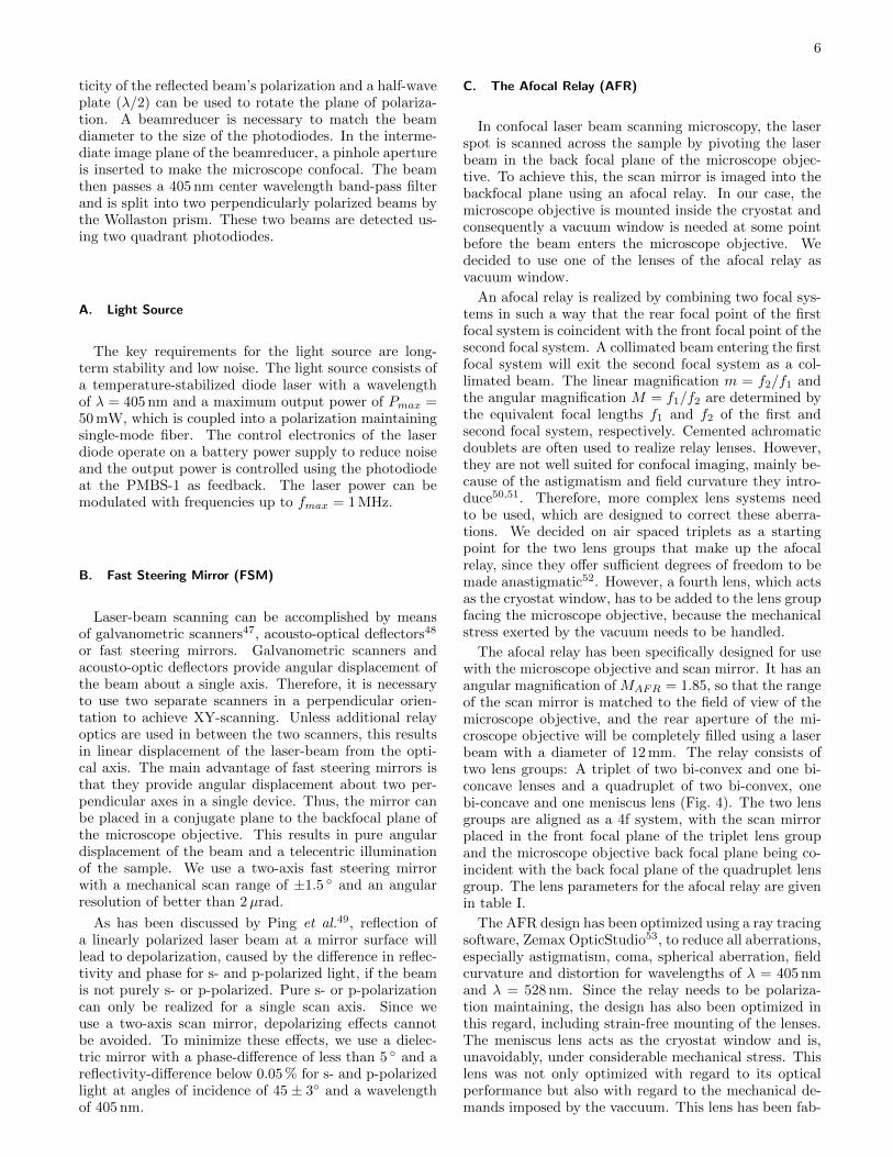
In confocal laser beam scanning microscopy, the laserspot is scanned across the sample by pivoting the laserbeam in the back focal plane of the microscope objec-tive. To achieve this, the scan mirror is imaged into thebackfocal plane using an afocal relay. In our case, themicroscope objective is mounted inside the cryostat andconsequently a vacuum window is needed at some pointbefore the beam enters the microscope objective. Wedecided to use one of the lenses of the afocal relay asvacuum window.
An afocal relay is realized by combining two focal sys-tems in such a way that the rear focal point of the firstfocal system is coincident with the front focal point of thesecond focal system. A collimated beam entering the firstfocal system will exit the second focal system as a col-limated beam. The linear magnification m = f2/f1 andthe angular magnification M = f1/f2 are determined bythe equivalent focal lengths f1 and f2 of the first andsecond focal system, respectively. Cemented achromaticdoublets are often used to realize relay lenses. However,they are not well suited for confocal imaging, mainly be-cause of the astigmatism and field curvature they intro-duce50,51. Therefore, more complex lens systems needto be used, which are designed to correct these aberra-tions. We decided on air spaced triplets as a startingpoint for the two lens groups that make up the afocalrelay, since they offer sufficient degrees of freedom to bemade anastigmatic52. However, a fourth lens, which actsas the cryostat window, has to be added to the lens groupfacing the microscope objective, because the mechanicalstress exerted by the vacuum needs to be handled.
The afocal relay has been specifically designed for usewith the microscope objective and scan mirror. It has anangular magnification of MAFR = 1.85, so that the rangeof the scan mirror is matched to the field of view of themicroscope objective, and the rear aperture of the mi-croscope objective will be completely filled using a laserbeam with a diameter of 12 mm. The relay consists oftwo lens groups: A triplet of two bi-convex and one bi-concave lenses and a quadruplet of two bi-convex, onebi-concave and one meniscus lens (Fig. 4). The two lensgroups are aligned as a 4f system, with the scan mirrorplaced in the front focal plane of the triplet lens groupand the microscope objective back focal plane being co-incident with the back focal plane of the quadruplet lensgroup. The lens parameters for the afocal relay are givenin table I.
The AFR design has been optimized using a ray tracingsoftware, Zemax OpticStudio53, to reduce all aberrations,especially astigmatism, coma, spherical aberration, fieldcurvature and distortion for wavelengths of λ = 405 nmand λ = 528 nm. Since the relay needs to be polariza-tion maintaining, the design has also been optimized inthis regard, including strain-free mounting of the lenses.The meniscus lens acts as the cryostat window and is,unavoidably, under considerable mechanical stress. Thislens was not only optimized with regard to its opticalperformance but also with regard to the mechanical de-mands imposed by the vaccuum. This lens has been fab-
7
FIG. 4. Layout of the afocal relay. Two lens groups, one triplet and one quadruplet, are used to relay the fast-steering mirror(FSM) onto the microscope objective’s back focal plane (MO-BFP). The FSM is placed in the entrance pupil on the left side,the MO-BFP is coincident with the exit pupil on the right side. The rightmost lens of the quadruplet, a meniscus lens, is usedas the cryostat window. The surface numbering is consistent with table I
TABLE I. Lens data for the AFR: Radius of curvature of thesurfaces defining the optical system and their separation alongthe optical axis. Material specifies the medium that fills thespace between the current surface and the next surface. Thesurface numbering is consistent with Fig. 4.
surfaceno.
radius[mm]
separation[mm]
material description
1 inf 119.637 air entrance pupil
2 159.604 9.809 N-LASF44 bi-convex
3 -159.604 14.000 air lens
4 -89.906 3.000 SF1 bi-concave
5 89.906 13.356 air lens
6 113.967 3.431 N-BAF10 bi-convex
7 -113.967 125.237 air lens
8 inf 82.248 air intermediateimage plane
9 50.810 3.647 N-LAF34 bi-convex
10 -61.500 4.945 air lens
11 -43.268 3.000 SF1 bi-concave
12 43.268 12.000 air lens
13 104.606 6.928 N-LAK33A bi-convex
14 -104.606 8.549 air lens
15 22.402 7.000 SF57HHT meniscus lensand cryostat
16 18.607 42.571 vacuum window
17 inf exit pupil
ricated from SF57HHT glass, which has an extremelylow stress-optical coefficient, to minimize stress birefrin-gence. Optical performance of the relay is diffractionlimited over the entire scan range, which is essential forconfocal imaging.
D. Beam Reducer, Confocal Pinhole and Resolution
The beam reducer is built from two commercial achro-matic doublets with a design wavelength of 405 nm. Theyhave equivalent focal lengths of fBR1 = 125 mm andfBR2 = 25 mm, so that the exiting beam is matched tothe photodiode diameter of 2.5 mm. The confocal pinholeaperture is mounted in the intermediate image plane ofthe beamreducer, which is a conjugate plane to the sam-ple, and consequently blocks light that is not originating
from the focal volume. The pinhole diameter dph is de-termined by the diameter of the airy disc and the mag-nification mcf = fBR1/(fMO ·MAFR) of the microscope.It is given in Airy units (AU), with 1 AU being the di-ameter of the image of the airy disc in the intermediateimage plane of the beamreducer. The 125 mm achromatwas selected, so that 1 AU = 10µm, with
1AU =1.22 · λNA
·mcf . (3)
The resolution in confocal microscopy is increased by28 % in comparison to widefield microscopy. In wide-field microscopy, the resolution is given by the distancebetween two points for which their point spread func-tions (PSF) can be distinguished and is expressed by theRayleigh criterion dmin = 0.61 · λ/NA. In the Rayleighcriterion, the point-spread function is described by theAiry disk. Two point sources are considered to be re-solvable, if the first minimum of the Airy disk of onepoint coincides with the global maximum of the other.In this case, the combined intensity profile shows a dipof ≈ 26 % between the maxima corresponding to the twopoints. The increase in resolution in confocal microscopyoriginates from the fact, that the confocal volume is de-fined by the product of the illumination PSF and theconvolution of the detection PSF with the pinhole27. Fora pinhole with a diameter of 0.5 AU, this results in afunction with a sharper peak compared to the widefieldPSF. In this case, the confocal resolution dcf is given by
dcf =0.44 · λNA
=0.44 · 405 nm
0.8= 222 nm . (4)
Using pinholes smaller than 0.5 AU does not increase theresolution, but deteriorates the SNR.
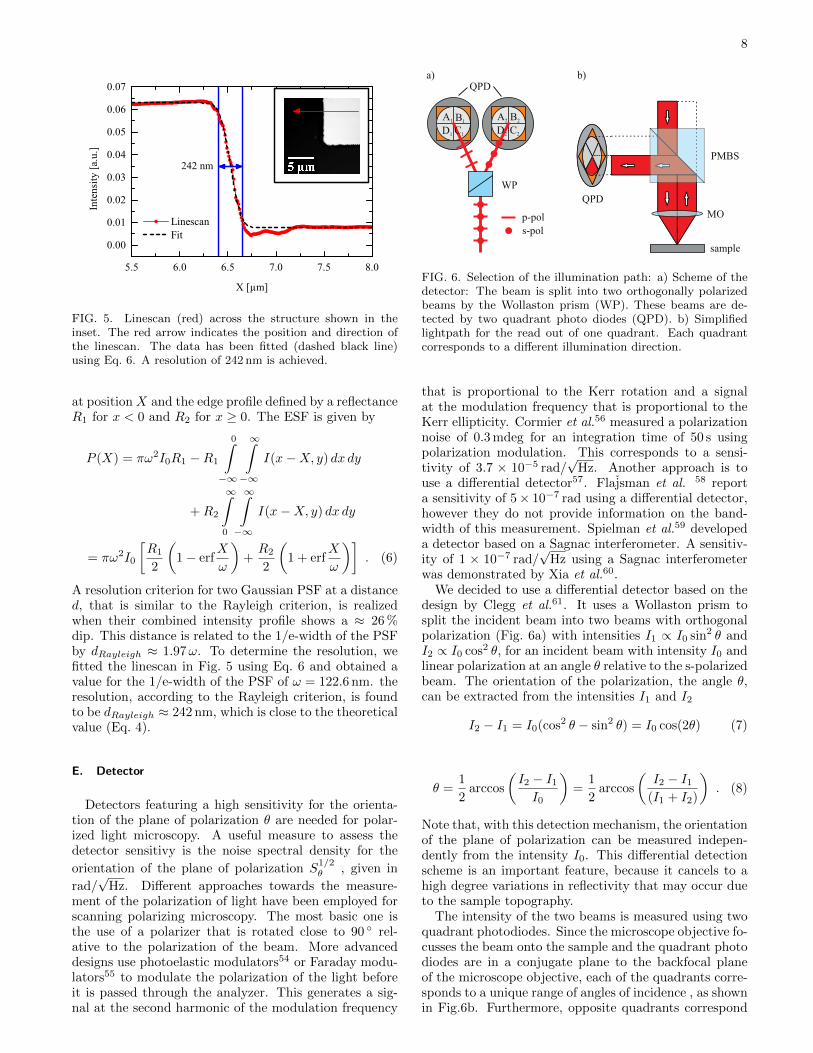
A linescan across the edge of a patterned structure isshown in Fig. 5. A confocal pinhole of 0.5 AU diameterwas used for the acquisition of the image and the lines-can. The intensity profile of the linescan can be usedto evaluate the width of the PSF and the correspond-ing resolution. For a Gaussian laser beam, the PSF hasa Gaussian profile with maximum intensity I0 and 1/e-width ω
I(x, y) = I0 e−(x2+y2)
ω2 . (5)
The edge-spread function (ESF), obtained by scanningover a sharp edge at x = 0, is the convolution of the PSF
8
5.5 6.0 6.5 7.0 7.5 8.0
0.00
0.01
0.02
0.03
0.04
0.05
0.06
0.07
Linescan Fit
In
tens
ity [a
.u.]
X [µm]
242 nm
FIG. 5. Linescan (red) across the structure shown in theinset. The red arrow indicates the position and direction ofthe linescan. The data has been fitted (dashed black line)using Eq. 6. A resolution of 242 nm is achieved.
at position X and the edge profile defined by a reflectanceR1 for x < 0 and R2 for x ≥ 0. The ESF is given by
P (X) = πω2I0R1 −R1
0∫−∞
∞∫−∞
I(x−X, y) dx dy
+R2
∞∫0
∞∫−∞
I(x−X, y) dx dy
= πω2I0
[R1
2
(1− erf
X
ω
)+R2
2
(1 + erf
X
ω
)]. (6)
A resolution criterion for two Gaussian PSF at a distanced, that is similar to the Rayleigh criterion, is realizedwhen their combined intensity profile shows a ≈ 26 %dip. This distance is related to the 1/e-width of the PSFby dRayleigh ≈ 1.97ω. To determine the resolution, wefitted the linescan in Fig. 5 using Eq. 6 and obtained avalue for the 1/e-width of the PSF of ω = 122.6 nm. theresolution, according to the Rayleigh criterion, is foundto be dRayleigh ≈ 242 nm, which is close to the theoreticalvalue (Eq. 4).
E. Detector
Detectors featuring a high sensitivity for the orienta-tion of the plane of polarization θ are needed for polar-ized light microscopy. A useful measure to assess thedetector sensitivy is the noise spectral density for the
orientation of the plane of polarization S1/2θ , given in
rad/√
Hz. Different approaches towards the measure-ment of the polarization of light have been employed forscanning polarizing microscopy. The most basic one isthe use of a polarizer that is rotated close to 90 ◦ rel-ative to the polarization of the beam. More advanceddesigns use photoelastic modulators54 or Faraday modu-lators55 to modulate the polarization of the light beforeit is passed through the analyzer. This generates a sig-nal at the second harmonic of the modulation frequency
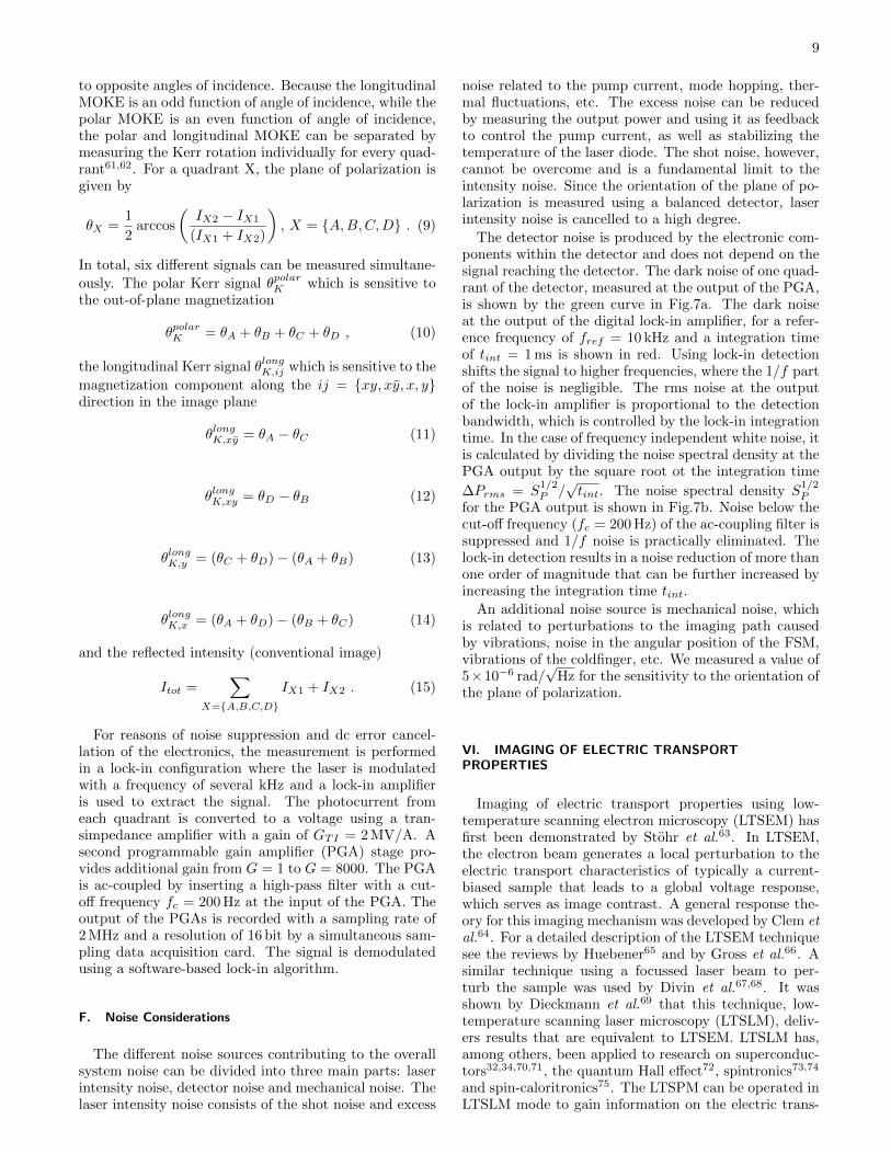
FIG. 6. Selection of the illumination path: a) Scheme of thedetector: The beam is split into two orthogonally polarizedbeams by the Wollaston prism (WP). These beams are de-tected by two quadrant photo diodes (QPD). b) Simplifiedlightpath for the read out of one quadrant. Each quadrantcorresponds to a different illumination direction.
that is proportional to the Kerr rotation and a signalat the modulation frequency that is proportional to theKerr ellipticity. Cormier et al.56 measured a polarizationnoise of 0.3 mdeg for an integration time of 50 s usingpolarization modulation. This corresponds to a sensi-tivity of 3.7 × 10⁻⁵ rad/
√Hz. Another approach is to
use a differential detector57. Flajsman et al. 58 reporta sensitivity of 5× 10⁻⁷ rad using a differential detector,however they do not provide information on the band-width of this measurement. Spielman et al.59 developeda detector based on a Sagnac interferometer. A sensitiv-ity of 1 × 10⁻⁷ rad/
√Hz using a Sagnac interferometer
was demonstrated by Xia et al.60.We decided to use a differential detector based on the
design by Clegg et al.61. It uses a Wollaston prism tosplit the incident beam into two beams with orthogonalpolarization (Fig. 6a) with intensities I1 ∝ I0 sin2 θ andI2 ∝ I0 cos2 θ, for an incident beam with intensity I0 andlinear polarization at an angle θ relative to the s-polarizedbeam. The orientation of the polarization, the angle θ,can be extracted from the intensities I1 and I2
I2 − I1 = I0(cos2 θ − sin2 θ) = I0 cos(2θ) (7)
θ =1
2arccos
(I2 − I1I0
)=
1
2arccos
(I2 − I1
(I1 + I2)
). (8)
Note that, with this detection mechanism, the orientationof the plane of polarization can be measured indepen-dently from the intensity I0. This differential detectionscheme is an important feature, because it cancels to ahigh degree variations in reflectivity that may occur dueto the sample topography.
The intensity of the two beams is measured using twoquadrant photodiodes. Since the microscope objective fo-cusses the beam onto the sample and the quadrant photodiodes are in a conjugate plane to the backfocal planeof the microscope objective, each of the quadrants corre-sponds to a unique range of angles of incidence , as shownin Fig.6b. Furthermore, opposite quadrants correspond
9
to opposite angles of incidence. Because the longitudinalMOKE is an odd function of angle of incidence, while thepolar MOKE is an even function of angle of incidence,the polar and longitudinal MOKE can be separated bymeasuring the Kerr rotation individually for every quad-rant61,62. For a quadrant X, the plane of polarization isgiven by
θX =1
2arccos
(IX2 − IX1
(IX1 + IX2)
), X = {A,B,C,D} . (9)
In total, six different signals can be measured simultane-
ously. The polar Kerr signal θpolarK which is sensitive tothe out-of-plane magnetization
θpolarK = θA + θB + θC + θD , (10)
the longitudinal Kerr signal θlongK,ij which is sensitive to the
magnetization component along the ij = {xy, xy, x, y}direction in the image plane
θlongK,xy = θA − θC (11)
θlongK,xy = θD − θB (12)
θlongK,y = (θC + θD)− (θA + θB) (13)
θlongK,x = (θA + θD)− (θB + θC) (14)
and the reflected intensity (conventional image)
Itot =∑
X={A,B,C,D}
IX1 + IX2 . (15)
For reasons of noise suppression and dc error cancel-lation of the electronics, the measurement is performedin a lock-in configuration where the laser is modulatedwith a frequency of several kHz and a lock-in amplifieris used to extract the signal. The photocurrent fromeach quadrant is converted to a voltage using a tran-simpedance amplifier with a gain of GTI = 2 MV/A. Asecond programmable gain amplifier (PGA) stage pro-vides additional gain from G = 1 to G = 8000. The PGAis ac-coupled by inserting a high-pass filter with a cut-off frequency fc = 200 Hz at the input of the PGA. Theoutput of the PGAs is recorded with a sampling rate of2 MHz and a resolution of 16 bit by a simultaneous sam-pling data acquisition card. The signal is demodulatedusing a software-based lock-in algorithm.
F. Noise Considerations
The different noise sources contributing to the overallsystem noise can be divided into three main parts: laserintensity noise, detector noise and mechanical noise. Thelaser intensity noise consists of the shot noise and excess
noise related to the pump current, mode hopping, ther-mal fluctuations, etc. The excess noise can be reducedby measuring the output power and using it as feedbackto control the pump current, as well as stabilizing thetemperature of the laser diode. The shot noise, however,cannot be overcome and is a fundamental limit to theintensity noise. Since the orientation of the plane of po-larization is measured using a balanced detector, laserintensity noise is cancelled to a high degree.
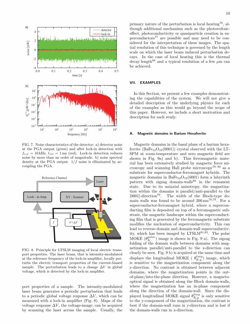
The detector noise is produced by the electronic com-ponents within the detector and does not depend on thesignal reaching the detector. The dark noise of one quad-rant of the detector, measured at the output of the PGA,is shown by the green curve in Fig.7a. The dark noiseat the output of the digital lock-in amplifier, for a refer-ence frequency of fref = 10 kHz and a integration timeof tint = 1 ms is shown in red. Using lock-in detectionshifts the signal to higher frequencies, where the 1/f partof the noise is negligible. The rms noise at the outputof the lock-in amplifier is proportional to the detectionbandwidth, which is controlled by the lock-in integrationtime. In the case of frequency independent white noise, itis calculated by dividing the noise spectral density at thePGA output by the square root ot the integration time
∆Prms = S1/2P /√tint. The noise spectral density S
1/2P
for the PGA output is shown in Fig.7b. Noise below thecut-off frequency (fc = 200 Hz) of the ac-coupling filter issuppressed and 1/f noise is practically eliminated. Thelock-in detection results in a noise reduction of more thanone order of magnitude that can be further increased byincreasing the integration time tint.
An additional noise source is mechanical noise, whichis related to perturbations to the imaging path causedby vibrations, noise in the angular position of the FSM,vibrations of the coldfinger, etc. We measured a value of5×10−6 rad/
√Hz for the sensitivity to the orientation of
the plane of polarization.
VI. IMAGING OF ELECTRIC TRANSPORTPROPERTIES
Imaging of electric transport properties using low-temperature scanning electron microscopy (LTSEM) hasfirst been demonstrated by Stohr et al.63. In LTSEM,the electron beam generates a local perturbation to theelectric transport characteristics of typically a current-biased sample that leads to a global voltage response,which serves as image contrast. A general response the-ory for this imaging mechanism was developed by Clem etal.64. For a detailed description of the LTSEM techniquesee the reviews by Huebener65 and by Gross et al.66. Asimilar technique using a focussed laser beam to per-turb the sample was used by Divin et al.67,68. It wasshown by Dieckmann et al.69 that this technique, low-temperature scanning laser microscopy (LTSLM), deliv-ers results that are equivalent to LTSEM. LTSLM has,among others, been applied to research on superconduc-tors32,34,70,71, the quantum Hall effect72, spintronics73,74
and spin-caloritronics75. The LTSPM can be operated inLTSLM mode to gain information on the electric trans-
10
101
102
103
104
105
106
10-4
10-3
10-2
10-1
100
101
S1/2
P [
pW
/√H
z]
frequency [Hz]
b)
0.0 0.1 0.2 0.3 0.4 0.5
-4
-2
0
2
4
no
ise [
nW
]
time [s]
detector
lock-in
a)
FIG. 7. Noise characteristics of the detector: a) detector noiseat the PGA output (green) and after lock-in detection withfref = 10 kHz, tint = 1 ms (red). Lock-in detection reducesnoise by more than an order of magnitude. b) noise spectraldensity at the PGA output. 1/f noise is elliminated by ac-coupling the PGA.
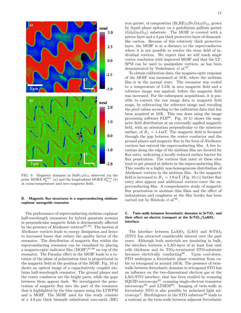
FIG. 8. Principle for LTSLM imaging of local electric trans-port properties. The laser beam, that is intensity-modulatedat the reference frequency of the lock-in amplifier, locally per-turbs the electric transport properties of the current-biasedsample. The perturbation leads to a change ∆V in globalvoltage, which is detected by the lock-in amplifier.
port properties of a sample. The intensity-modulatedlaser beam generates a periodic perturbation that leadsto a periodic global voltage response ∆V , which can bemeasured with a lock-in amplifier (Fig. 8). Maps of thevoltage response ∆V , the voltage-image, can be acquiredby scanning the laser across the sample. Usually, the
primary nature of the perturbation is local heating76, al-though additional mechanism such as the photovoltaic-effect, photoconductivity or quasiparticle creation in su-perconductors77 are possible and may need to be con-sidered for the interpretation of these images. The spa-tial resolution of this technique is governed by the lengthscale on which the laser beam induced perturbation de-cays. In the case of local heating this is the thermaldecay length66 and a typical resolution of a few µm canbe achieved.
VII. EXAMPLES
In this Section, we present a few examples demonstrat-ing the capabilities of the system. We will not give adetailed description of the underlying physics for eachof the examples as this would go beyond the scope ofthis paper. However, we include a short motivation anddescription for each study.
A. Magnetic domains in Barium Hexaferrite
Magnetic domains in the basal plane of a barium hexa-ferrite (BaFe12O19(0001)) crystal observed with the LT-SPM at room-temperature and zero magnetic field areshown in Fig. 9a) and b). This ferromagnetic mate-rial has been extensively studied by magnetic force mi-croscopy and scanning Hall probe microscopy78–80 as asubstrate for superconductor-ferromagnet hybrids. Themagnetic domains in BaFe12O19(0001) form a labyrinthpattern with zigzag domain-walls80 in the remanentstate. Due to its uniaxial anisotropy, the magnetiza-tion within the domains is parallel/anti-parallel to the[0001]-direction79. The width of the Bloch-type do-main walls was found to be around 200 nm78,79. For asuperconductor-ferromagnet hybrid, where a supercon-ducting film is deposited on top of a ferromagnetic sub-strate, the magnetic landscape within the superconduct-ing film that is generated by the ferromagnetic substratemodifies the nucleation of superconductivity. This canlead to reverse-domain and domain-wall superconductiv-ity, which has been imaged by LTSLM81,82. The polar
MOKE (θpolarK ) image is shown in Fig. 9 a). The zigzagfolding of the domain walls between domains with mag-netization parallel/anti-parallel to the z-direction canclearly be seen. Fig. 9 b) is acquired at the same time and
displays the longitudinal MOKE ( θlongK,y ) image, whichis sensitive to the magnetization component along they-direction. No contrast is obtained between adjacentdomains, where the magnetization points in the out-of-plane/into-the-plane direction. However, a magneto-optical signal is obtained along the Bloch domain-walls,where the magnetization has an in-plane componentalong the direction of the domain-wall. Since the dis-
played longitudinal MOKE signal θlongK,y is only sensitiveto the y-component of the magnetization, the contrast isbest if the domain-wall runs in y-direction and is lost ifthe domain-walls run in x-direction.
11
FIG. 9. Magnetic domains in BaFe12O19 observed via thepolar MOKE θpolarK (a) and the longitudinal MOKE θlong
K,y (b)at room-temperature and zero magnetic field.
B. Magnetic flux structures in a superconducting niobiumcoplanar waveguide resonator
The performance of superconducting niobium coplanarhalf-wavelength resonators for hybrid quantum systemsin perpendicular magnetic fields is detrimentally affectedby the presence of Abrikosov vortices83–85. The motion ofAbrikosov vortices leads to energy dissipation and henceto increased losses that reduce the quality factor of theresonator. The distribution of magnetic flux within thesuperconducting resonator can be visualized by placinga magneto-optic indicator film (MOIF)41,86 on top of theresonator. The Faraday effect in the MOIF leads to a ro-tation of the plane of polarization that is proportional tothe magnetic field at the position of the MOIF. Fig. 10 a)shows an optical image of a capacitatively coupled nio-bium half-wavelength resonator. The ground planes andthe center conductor are the bright parts, while the gapsbetween them appear dark. We investigated the pene-tration of magnetic flux into the part of the resonatorthat is highlighted by the blue square using the LTWPMand a MOIF. The MOIF used for this study consistsof a 4.9µm thick bismuth substituted rare-earth (RE)
iron garnet, of composition (Bi,RE)3(Fe,Ga)5O12, grownby liquid phase epitaxy on a gadolinium gallium garnet(Gd3Ga5O12) substrate. The MOIF is covered with amirror layer and a 4µm thick protective layer of diamond-like carbon. Because of this relatively thick protectivelayer, the MOIF is at a distance to the superconductorwhere it is not possible to resolve the stray field of in-dividual vortices. We expect that we will reach singlevortex resolution with improved MOIF and that the LT-SPM can be used to manipulate vortices, as has beendemonstrated by Veshchunov et al.87.
To obtain calibration data, the magneto-optic responseof the MOIF was measured at 10 K, where the niobiumfilm is in the normal state. The resonator was cooledto a temperature of 5.3 K in zero magnetic field and areference image was aquired, before the magnetic fieldwas increased. For the subsequent acquisitions, it is pos-sible to convert the raw image data to magnetic fieldmaps, by subtracting the reference image and rescalingthe pixel values according to the calibration data that hasbeen acquired at 10 K. This was done using the imageprocessing software FIJI88. Fig. 10 b) shows the mag-netic field distribution at an externally applied magneticfield, with an orientation perpendicular to the substratesurface, of B⊥ = 1.4 mT. The magnetic field is focussedthrough the gap between the center conductor and theground planes and magnetic flux in the form of Abrikosovvortices has entered the superconducting film. A few lo-cations along the edge of the niobium film are favored forflux entry, indicating a locally reduced surface barrier forflux penetration. The vortices that enter at these sitestend to get pinned at defects in the superconducting film.This results in a highly non-homogeneous distribution ofAbrikosov vortices in the niobium film. As the magneticfield is increased to B⊥ = 1.8 mT (Fig. 10 c)) further fluxentry sites appear and additional vortices enter the su-perconducting film. A comprehensive study of magneticflux penetration in niobium thin films and the effect ofindentations and roughness at the film border has beencarried out by Brisbois et al.89.
C. Twin-walls between ferroelastic domains in SrTiO3 andtheir effect on electric transport at the SrTiO3/LaAlO3
interface
The interface between LaAlO3 (LAO) and SrTiO3
(STO) has attracted considerable interest over the pastyears. Although both materials are insulating in bulk,the interface between a LAO-layer of at least four unitcells thickness and its TiO2-terminated STO-substratebecomes electrically conducting90. Upon cool-down,STO undergoes a ferroelastic phase transition from cu-bic to tetragonal at around 105 K. The presence of twin-walls between ferroelastic domains in tetragonal STO hasan influence on the two-dimensional electron gas at theLAO/STO interface, that has been studied by scanningSQUID microscopy91, scanning single-electron transistormicroscopy92 and LTSEM93. Imaging of twin-walls inferroelastic STO is also possible by polarized light mi-croscopy2. Birefringence in the STO substrate94 leads toa contrast at the twin-walls between adjacent ferroelastic
12
FIG. 10. Optical image of a superconducting niobium half-wavelength resonator (a). The ground plane and center con-ductor appear bright, the gaps between them appear dark.The blue square indicates the area that has been imaged in(b) and (c) using a MOIF and the LTWPM. Magnetic fielddistribution above the resonator at an externally applied fieldof B⊥ = 1.4 mT (b) and B⊥ = 1.8 mT (c) at a temperatureof 5.3 K.
domains.
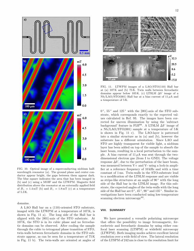
A LAO Hall bar on a (110)-oriented STO substrate,imaged with the LTWPM at a temperature of 107 K, isshown in Fig. 11 a). The long side of the Hall bar isaligned with the [001]-axis of the STO substrate. At107 K, the STO is in its cubic phase and no ferroelas-tic domains can be observed. After cooling the samplethrough the cubic to tetragonal phase transition of STO,twin-walls between ferroelastic domains in the STO sub-strate appear, as can be seen for a temperature of 75 Kin Fig. 11 b). The twin-walls are oriented at angles of
FIG. 11. LTWPM images of a LAO/STO(110) Hall barat (a) 107 K and (b) 75 K. Twin walls between ferroelasticdomains appear below 105 K. (c) LTSLM ∆V image of aNb/LAO/STO(001) Hall bar at a bias current of 11µA anda temperature of 5 K.
0 ◦, 55 ◦ and 125 ◦ with the [001]-axis of the STO sub-strate, which corresponds exactly to the expected val-ues calculated in Ref. 93. The images have been cor-rected for uneven illumination by using the ’subtractbackground’ feature in FIJI88. A LTSLM ∆V image ofa Nb/LAO/STO(001) sample at a temperature of 5 Kis shown in Fig. 11 c). The LAO-layer is patternedinto a similar structure as in (a) and (b), however thesubstrate has a different orientation. Since LAO andSTO are highly transparent for visible light, a niobiumlayer has been added on top of the sample to absorb thelaser beam, resulting in a local perturbation to the sam-ple. A bias current of 11µA was sent through the two-dimensional electron gas (from I to GND). The voltageresponse ∆V , due to the perturbation of the laser beam,was measured between V+ and V- using a lock-in ampli-fier at a reference frequency of 10 kHz and with a timeconstant of 1 ms. Twin-walls in the STO-substrate leadto a modification of the LTSLM response and are visibleas stripe-like structures at an angle of 90 ◦ with the longside of the Hall bar in the LTSLM image. For this sub-strate, the expected angles of the twin-walls with the longside of the Hall bar are 0 ◦, 45 ◦, 90 ◦ and 135 ◦. Similar in-vestigations have been conducted using low-temperaturescanning electron microscopy93.
VIII. SUMMARY
We have presented a versatile polarizing microscopethat offers the possibility to image ferromagnetic, fer-roelectric and ferroelastic domains by using either con-focal laser scanning (LTSPM) or widefield microscopy(LTWPM). Both imaging modes achieve excellent lateralresolution over a wide field of view. The lateral resolutionof the LTSPM of 242 nm is close to the resolution limit for
13
TABLE II. system specifications
LTSPM LTWPM
resolution 242 nm 481 nm
sensitivity 5× 10⁻⁶ rad/√
Hz 1.0× 10⁻⁴ rad/√
Hz
field of view 500µm× 500µm
temperature range 4 K to 300 K
B‖ ±800 mT
B⊥ ±20 mT
imaging with visible light. The instrument is equippedwith highly sensitive polarized light detectors that pro-vide a sensitivity of 1.0×10⁻⁴ rad/
√Hz for the LTWPM
and 5×10⁻⁶ rad/√
Hz for the LTSPM. A 4He continuousflow cryostat enables observations at sample tempera-tures ranging from 4 K to 300 K, and magnetic fields withvariable orientation can be applied to the sample. Thesystem specifications are summarized in table II. We havedemonstrated the capability of the microscope to imageferromagnetic domains and domain-walls in BaFe12O19,ferroelastic domains in SrTiO3, the magnetic field dis-tribution above a superconducting Nb film and electri-cal transport characteristics of the 2-dimensional elec-tron gas at the interface of LaAlO3 and SrTiO3. Weexpect that the instrument will prove to be useful for in-vestigations of a wide variety of solid-state effects. Thecombination of magnetic, structural and electric imagingwith high lateral resolution and variable temperature hasthe potential to deliver important insights for research inspintronics, spin caloritronics, superconductivity, mag-netism and their hybrid-systems.
ACKNOWLEDGMENTS
We thank J. Fritzsche for providing the BaFe12O19
crystal, D. Bothner and B. Ferdinand for providing theNb resonator, M. Lindner (Innovent e.V. Jena) for pro-viding the MOIF, and H.J.H Ma and A. Stohr for pro-viding the LAO/STO samples. This work was funded bythe Deutsche Forschungsgemeinschaft (DFG) via projectNo. KO 1303/8-1.
1J. McCord, J. Phys. D: Appl. Phys. 48, 333001 (2015).2Z. Erlich, Y. Frenkel, J. Drori, Y. Shperber, C. Bell, H. K. Sato,M. Hosoda, Y. Xie, Y. Hikita, H. Y. Hwang, and B. Kalisky, J.Supercond. Novel Magn. 28, 1017 (2015).
3Z.-G. Ye and M. Dong, J. Appl. Phys. 87, 2312 (2000).4C.-S. Tu, C.-L. Tsai, V. H. Schmidt, H. Luo, and Z. Yin, J.Appl. Phys. 89, 7908 (2001).
5F. Bitter, Phys. Rev. 41, 507 (1932).6J. Jakubovics, “Lorentz microscopy,” in Handbook of Microscopy,Vol. 1, edited by S. Amelinckx (VCH, Weinheim, New York,1997) pp. 505–514.
7A. Tonomura, J. Magn. Magn. Mater. 31, 963 (1983).8U. Hartmann, Annu. Rev. Mater. Sci. 29, 53 (1999).9J. R. Kirtley and J. P. Wikswo, Annu. Rev. Mater. Sci. 29, 117(1999).
10A. M. Chang, H. D. Hallen, L. Harriott, H. F. Hess, H. L. Kao,J. Kwo, R. E. Miller, R. Wolfe, J. van der Ziel, and T. Y. Chang,Appl. Phys. Lett. 61, 1974 (1992).
11B. J. Maertz, A. P. Wijnheijmer, G. D. Fuchs, M. E. Nowakowski,and D. D. Awschalom, Appl. Phys. Lett. 96, 092504 (2010).
12C. Schneider, J. Magn. Magn. Mater. 175, 160 (1997).
13H. Akamine, S. Okumura, S. Farjami, Y. Murakami, andM. Nishida, Sci. Rep. 6, 37265 (2016).
14M. R. Scheinfein, J. Unguris, M. H. Kelley, D. T. Pierce, andR. J. Celotta, Rev. Sci. Instrum. 61, 2501 (1990).
15A. Hubert and R. Schafer, Magnetic Domains: The Analysis ofMagnetic Microstructures (Springer, 1998).
16J. A. Hooton and W. J. Merz, Phys. Rev. 98, 409 (1955).17C. Ke, X. Wang, X. P. Hu, S. N. Zhu, and M. Qi, J. Appl. Phys.101, 064107 (2007).
18V. V. Aristov, L. S. Kokhanchik, and Y. I. Voronovskii, physicastatus solidi (a) 86, 133 (1984).
19P. Guthner and K. Dransfeld, Appl. Phys. Lett. 61, 1137 (1992).20G. Fogarty, B. Steiner, M. Cronin-Golomb, U. Laor, M. H. Gar-
rett, J. Martin, and R. Uhrin, J. Opt. Soc. Am. B 13, 2636(1996).
21P. R. Potnis, N.-T. Tsou, and J. E. Huber, Materials 4, 417(2011).
22E. Soergel, Appl. Phys. B 81, 729 (2005).23H. Schmid, “Polarized light microscopy (plm) of ferroelectric and
ferroelastic domains in transmitted and reflected light,” in Fer-roelectric Ceramics: Tutorial reviews, theory, processing, andapplications, edited by N. Setter and E. L. Colla (BirkhauserBasel, Basel, 1993) pp. 107–126.
24R. M. Grechishkin, O. V. Malyshkina, and S. S. Soshin, Ferro-electrics 222, 215 (1999).
25J. Kerr, Philos. Mag. 3, 321 (1877).26M. Faraday, Philos. Trans. Roy. Soc. London 136, 1 (1846).27R. H. Webb, Rep. Prog. Phys. 59, 427 (1996).28S. Inoue and R. Oldenbourg, “Optical Instruments: micro-
scopes,” in Handbook of Optics 2nd edition, Vol. 2, edited byM. Bass (McGraw-Hill, New York, 1994) Chap. 17.
29S. Guenon, Cryogenic Scanning Laser Microscopy: Investigationof large BSCCO mesas and development of a polarizing micro-scope, Ph.D. thesis, Universitat Tubingen (2011).
30A. Kittel, P. Stagge, and J. Parisi, Rev. Sci. Instrum. 68, 1286(1997).
31P. Li, D. Abraimov, A. Polyanskii, F. Kametani, and D. Lar-balestier, Phys. Rev. B 91, 104504 (2015).
32T. M. Benseman, A. E. Koshelev, V. Vlasko-Vlasov, Y. Hao,W.-K. Kwok, U. Welp, C. Keiser, B. Gross, M. Lange, D. Kolle,R. Kleiner, H. Minami, C. Watanabe, and K. Kadowaki, Phys.Rev. Applied 3, 044017 (2015).
33A. G. Sivakov, A. V. Lukashenko, D. Abraimov, P. Muller, A. V.Ustinov, and M. Leghissa, Appl. Phys. Lett. 76, 2597 (2000).
34H. B. Wang, S. Guenon, J. Yuan, A. Iishi, S. Arisawa, T. Hatano,T. Yamashita, D. Koelle, and R. Kleiner, Phys. Rev. Lett. 102,017006 (2009).
35H. Kirchner, Rev. Sci. Instrum. 44, 379 (1973).36P. E. Goa, H. Hauglin, A. A. F. Olsen, M. Baziljevich, and T. H.
Johansen, Rev. Sci. Instrum. 74, 141 (2003).37D. Golubchik, E. Polturak, G. Koren, and S. G. Lipson, Opt.
Express 17, 16160 (2009).38T. Henn, T. Kiessling, W. Ossau, L. W. Molenkamp, K. Bier-
mann, and P. V. Santos, Rev. Sci. Instrum. 84, 123903 (2013).39H. Murakami and M. Tonouchi, Rev. Sci. Instrum. 81, 013701
(2010).40S. Matsuzaka, Y. Ohno, and H. Ohno, J. Supercond. Novel
Magn. 23, 37 (2009).41P. Gornert, A. Lorenz, M. Lindner, and H. Richert, “Magneto-
optic garnet sensor films: Preparation, characterization, applica-tion,” in Crystal Growth Technology (Wiley-VCH Verlag GmbH& Co. KGaA, 2010) pp. 249–266.
42A. Kohler, Z. Wiss. Mikrosk. Mikroskopisc. Tech 10, 433 (1893).43I. V. Soldatov and R. Schafer, Phys. Rev. B 95, 014426 (2017).44I. V. Soldatov and R. Schafer, Rev. Sci. Instrum. 88, 073701
(2017).45A. Stupakiewicz, A. Chizhik, M. Tekielak, A. Zhukov, J. Gon-
zalez, and A. Maziewski, Rev. Sci. Instrum. 85 (2014),10.1063/1.4896758.
46M. I. Shribak, S. Inoue, and R. Oldenbourg, Opt. Eng. 41, 41(2002).
47J. Montagu, “Galvanometric and resonant scanners,” in Hand-book of Optical and Laser-Scanning, Second Edition (CRC Press,2011) pp. 393–448.
14
48X. Lv, C. Zhan, S. Zeng, W. R. Chen, and Q. Luo, Rev. Sci.Instrum. 77, 046101 (2006).
49G. L. Ping, C. W. See, M. G. Somekh, M. B. Suddendorf, J. H.Vincent, and P. K. Footner, Scanning 18, 8 (1996).
50A. C. Ribes, S. Damaskinos, and A. E. Dixon, Scanning 22, 282(2000).
51A. Negrean and H. D. Mansvelder, Biomed. Opt. Express 5, 1588(2014).
52M. Laikin, Lens Design, Fourth Edition, Optical Science andEngineering (CRC Press, 2006).
53“Zemax OpticStudio,” http://customers.zemax.com/os/
opticstudio.54P. Vavassori, Appl. Phys. Lett. 77, 1605 (2000).55H. Hornauer, T. M. Atmono, and K. Roll, J. Magn. Magn. Mater.83, 551 (1990).
56M. Cormier, J. Ferre, A. Mougin, J.-P. Cromieres, and V. Klein,Rev. Sci. Instrum. 79, 033706 (2008).
57P. Kasiraj, R. Shelby, J. Best, and D. Horne, IEEE Trans. Magn.22, 837 (1986).
58L. Flajsman, M. Urbanek, V. Krizakova, M. Vanatka, I. Turcan,and T. Sikola, Rev. Sci. Instrum. 87, 053704 (2016).
59S. Spielman, K. Fesler, C. B. Eom, T. H. Geballe, M. M. Fejer,and A. Kapitulnik, Phys. Rev. Lett. 65, 123 (1990).
60J. Xia, P. T. Beyersdorf, M. M. Fejer, and A. Kapitulnik, Appl.Phys. Lett. 89, 062508 (2006).
61W. Clegg, N. Heyes, E. Hill, and C. Wright, J. Magn. Magn.Mater. 95, 49 (1991).
62H. Ding, S. Putter, H. Oepen, and J. Kirschner, J. Magn. Magn.Mater. 212, 5 (2000).
63P. L. Stohr and R. P. Huebener, J. Low Temp. Phys. 37, 277(1979).
64J. R. Clem and R. P. Huebener, J. Appl. Phys. 51, 2764 (1980).65R. Huebener, Advances in Electronics and Electron Physics 70,
1 (1988).66R. Gross and D. Koelle, Rep. Prog. Phys. 57, 651 (1994).67Y. Y. Divin, F. Y. Nad’, V. Y. Pokrovski, and P. M. Shadrin,
IEEE Trans. Magn. 27, 1101 (1991).68Y. Divin and P. Shadrin, Physica C 232, 257 (1994).69N. Dieckmann, S. Friemel, A. Bock, U. Merkt, R. Gerber, and
R. Huebener, Physica C 292, 133 (1997).70A. Sivakov, A. Zhuravel’, O. Turutanov, and I. Dmitrenko, Appl.
Surf. Sci. 106, 390 (1996), proceedings of the Second Interna-tional Conference on Photo-Excited Processes and Applications.
71R. Werner, A. Y. Aladyshkin, I. M. Nefedov, A. V. Putilov,M. Kemmler, D. Bothner, A. Loerincz, K. Ilin, M. Siegel,R. Kleiner, and D. Koelle, Supercond. Sci. Technol. 26, 095011(2013).
72A. A. Shashkin, A. J. Kent, J. R. Owers-Bradley, A. J. Cross,P. Hawker, and M. Henini, Phys. Rev. Lett. 79, 5114 (1997).
73M. Wagenknecht, H. Eitel, T. Nachtrab, J. B. Philipp, R. Gross,R. Kleiner, and D. Koelle, Phys. Rev. Lett. 96, 047203 (2006).
74R. Werner, M. Weiler, A. Y. Petrov, B. A. Davidson, R. Gross,R. Kleiner, S. T. B. Goennenwein, and D. Koelle, Appl. Phys.Lett. 99, 182513 (2011).
75M. Weiler, M. Althammer, F. D. Czeschka, H. Huebl, M. S. Wag-ner, M. Opel, I.-M. Imort, G. Reiss, A. Thomas, R. Gross, andS. T. B. Goennenwein, Phys. Rev. Lett. 108, 106602 (2012).
76A. P. Zhuravel, A. G. Sivakov, O. G. Turutanov, A. N. Omelyan-chouk, S. M. Anlage, A. Lukashenko, A. V. Ustinov, andD. Abraimov, Low Temp. Phys. 32, 592 (2006).
77A. Zhuravel, A. Ustinov, D. Abraimov, and S. Anlage, IEEETransactions on Applied Superconductivity 13, 340 (2003).
78Z. Yang, M. Lange, A. Volodin, R. Szymczak, and V. V.Moshchalkov, Nat. Mater. 3, 793 (2004).
79Z. Yang, K. Vervaeke, V. V. Moshchalkov, and R. Szymczak,Phys. Rev. B 73, 224509 (2006).
80Z. Yang, J. Fritzsche, and V. V. Moshchalkov, Appl. Phys. Lett.98, 012505 (2011).
81J. Fritzsche, V. V. Moshchalkov, H. Eitel, D. Koelle, R. Kleiner,and R. Szymczak, Phys. Rev. Lett. 96, 247003 (2006).
82R. Werner, A. Y. Aladyshkin, S. Guenon, J. Fritzsche, I. M.Nefedov, V. V. Moshchalkov, R. Kleiner, and D. Koelle, Phys.Rev. B 84, 020505 (2011).
83D. Bothner, T. Gaber, M. Kemmler, D. Koelle, and R. Kleiner,Appl. Phys. Lett. 98, 102504 (2011).
84D. Bothner, C. Clauss, E. Koroknay, M. Kemmler, T. Gaber,M. Jetter, M. Scheffler, P. Michler, M. Dressel, D. Koelle, andR. Kleiner, Supercond. Sci. Technol. 25, 065020 (2012).
85D. Bothner, T. Gaber, M. Kemmler, D. Koelle, R. Kleiner,S. Wunsch, and M. Siegel, Phys. Rev. B 86, 014517 (2012).
86T. Johansen and D. Shantsev, Magneto-Optical Imaging, NatoScience Series II: (Springer Netherlands, 2004).
87I. S. Veshchunov, W. Magrini, S. V. Mironov, A. G. Godin, J.-B.Trebbia, A. I. Buzdin, P. Tamarat, and B. Lounis, Nat. Com-mun. 7, 12801 (2016).
88J. Schindelin, I. Arganda-Carreras, E. Frise, V. Kaynig, M. Lon-gair, T. Pietzsch, S. Preibisch, C. Rueden, S. Saalfeld, B. Schmid,J.-Y. Tinevez, D. J. White, V. Hartenstein, K. Eliceiri, P. Toman-cak, and A. Cardona, Nat. Methods 9, 676 (2012).
89J. Brisbois, O.-A. Adami, J. I. Avila, M. Motta, W. A. Ortiz,N. D. Nguyen, P. Vanderbemden, B. Vanderheyden, R. B. G.Kramer, and A. V. Silhanek, Phys. Rev. B 93, 054521 (2016).
90A. Ohtomo and H. Y. Hwang, Nature 427, 423 (2004).91B. Kalisky, E. M. Spanton, H. Noad, J. R. Kirtley, K. C. Nowack,
C. Bell, H. K. Sato, M. Hosoda, Y. Xie, Y. Hikita, C. Woltmann,G. Pfanzelt, R. Jany, C. Richter, H. Y. Hwang, J. Mannhart,and K. A. Moler, Nature Mater. 12, 1091 (2013).
92M. Honig, J. A. Sulpizio, J. Drori, A. Joshua, E. Zeldov, andS. Ilani, Nature Mater. 12, 1112 (2013).
93H. J. H. Ma, S. Scharinger, S. W. Zeng, D. Kohlberger, M. Lange,A. Stohr, X. R. Wang, T. Venkatesan, R. Kleiner, J. F. Scott,J. M. D. Coey, D. Koelle, and Ariando, Phys. Rev. Lett. 116,257601 (2016).
94M. A. Geday and A. M. Glazer, J. Phys.: Condens. Matter 16,3303 (2004).