Embed Size (px)
Citation preview
REV. 0
Information furnished by Analog Devices is believed to be accurate andreliable. However, no responsibility is assumed by Analog Devices for itsuse, nor for any infringements of patents or other rights of third partieswhich may result from its use. No license is granted by implication orotherwise under any patent or patent rights of Analog Devices.
aADP3020
One Technology Way, P.O. Box 9106, Norwood, MA 02062-9106, U.S.A.
Tel: 781/329-4700 World Wide Web Site: http://www.analog.com
Fax: 781/326-8703 © Analog Devices, Inc., 2000
High-Efficiency Notebook ComputerPower Supply Controller
FUNCTIONAL BLOCK DIAGRAM
POWER-ONRESET
LINEARCONTROLLER
VIN5.5V TO 25V
3.3V
Q5
2.5V
SS3
Q1
Q2
Q3
SS5
Q4
5VL1L2
PWRGD
ADP3020
REF
5V LINEAR
3.3VSMPS
5VSMPS
1.20V
PFO
3.3VSMPS
FEATURES
Wide Input Voltage Range: 4.5 V to 25 V
High Conversion Efficiency > 96%
Integrated Current Sense—No External Resistor Required
Low Shutdown Current: 7 A (Typical)
Dual Synchronous Buck Controllers with Selectable
PWM/Power-Saving Mode Operation
Built-In Gate Drive Boost Circuit for Driving External
N-Channel MOSFETs
Two Independently Programmable Output Voltages
Fixed 3.3 V or Adjustable (1.25 V to VIN–0.5 V)
Fixed 5 V or Adjustable (1.25 V to VIN–0.5 V)
Programmable PWM Frequency
Integrated Linear Regulator Controller
Extensive Circuit Protection Functions
38-Lead TSSOP Package
APPLICATIONS
Notebook Computers and PDAs
Portable Instruments
General Purpose DC-DC Converters
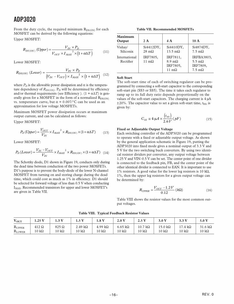
GENERAL DESCRIPTIONThe ADP3020 is a highly efficient dual synchronous buck switch-ing regulator controller optimized for converting the battery oradapter input into the system supply voltages required in note-book computers. The ADP3020 uses a dual-mode PWM/PowerSaving Mode architecture to maintain efficiency over a wideload range. The oscillator frequency can be programmed for200 kHz, 300 kHz, or 400 kHz operation, or it can be synchro-nized to an external clock signal of up to 600 kHz.
The ADP3020 provides accurate and reliable short circuit pro-tection using an internal current sense circuit, which reducescost and increases overall efficiency. Other protection featuresinclude programmable soft-start, UVLO, and integrated outputundervoltage/overvoltage protection. The ADP3020 contains alinear regulator controller that is designed to drive an externalP-channel MOSFET or PNP transistor. The linear regulatoroutput is adjustable, and can be used to generate the auxiliaryvoltages required in many laptop designs.
–2– REV. 0
ADP3020–SPECIFICATIONS (@ TA = –40C to +85C, VIN = 12 V, SS5 = SS3 = INTVCC, INTVCC Load = 0 mA,REF Load = 0 mA, MODE = 0 V, SYNC = 0 V, SD = 5 V, unless otherwise noted.)
Parameter Symbol Conditions Min Typ Max Unit
INTERNAL 5 V REGULATOR INTVCCInput Voltage Range 5.5 25 V5 V Voltage TA = 25°C 4.95 5.025 5.15 VLine Regulation 5.5 V ≤ VIN ≤ 25 V 0.3 mV/VTotal Variation Line, Temp 4.8 5.2 VSwitchover Voltage AUXVCC from Low to High 4.65 4.75 4.85 VSwitchover Hysteresis AUXVCC from High to Low 100 mVUndervoltage Lockout INTVCC Falling 3.6 3.8 4.2 VThreshold VoltageUndervoltage Lockout 120 mVHysteresis
REFERENCEOutput Voltage2 REF 5.5 V ≤ VIN ≤ 25 V 1.185 1.197 1.209 V
SUPPLY CURRENT IQ
Shutdown Current SD = 0 V 7 15 µAStandby Current SS3 = SS5 = SD2 = 0 V 250 400 µA
SD = 5 VQuiescent Current No Loads, MODE = 5 V 0.95 1.8 mA(PWM Mode) SS3 = SS5 = SD2 = 5 V
FB5 = FB3 = FB2 = 1.25 V,ADJ/FX5 = ADJ/FX3 = 5 V
Quiescent Current No Loads, MODE = 0 V 650 µA(Power-Saving Mode) SS3 = SS5 = SD2 = 5 V
FB5 = FB3 = FB2 = 1.25 V,ADJ/FX5 = ADJ/FX3 = 5 V
OSCILLATORFrequency fOSC SYNC = AGND 176 200 224 kHz
SYNC = REF 264 300 336 kHzSYNC = INTVCC 352 400 448 kHz
SYNC InputFrequency Range 230 600 kHzInput Low Voltage3 tF ≤ 200 ns 0.4 VInput High Voltage3 tR ≤ 200 ns 4.6 VInput Current SYNC = REF 1.2 µA
POWER GOOD PWRGDOutput Voltage In Regulation 10 kΩ Pull-Up to 5 V 4.8 VOutput Voltage Out of Regulation 10 kΩ Pull-Up to 5 V 0.4 V
FB5 < 90% of NominalOutput Value
PWRGD Trip Threshold FB5 Rising –8 –4 –2 %PWRGD Hysteresis FB5 Falling 4 %CPOR Pull-Up Current CPOR = 1.2 V 2.5 µA
ERROR AMPLIFIERDC Gain 67 dBGain-Bandwidth Product GBW 10 MHzInput Leakage Current IEAN ADJ/FX5 = ADJ/FX3 = 5 V 200 nA
MAIN SMPS CONTROLLERSFixed 5 V Output Voltage FB5
PWM Mode 5.5 V ≤ VIN ≤ 25 V, ADJ/FX5 = 0 V 4.90 5.0 5.10 VPower-Saving Mode 5.5 V ≤ VIN ≤ 25 V, ADJ/FX5 = 0 V 4.925 5.025 5.125 V
Fixed 3.3 V Output Voltage FB3PWM Mode 5.5 V ≤ VIN ≤ 25 V, ADJ/FX3 = 0 V 3.234 3.3 3.366 VPower-Saving Mode 5.5 V ≤ VIN ≤ 25 V, ADJ/FX3 = 0 V 3.250 3.316 3.382 V
–3–REV. 0
ADP3020Parameter Symbol Conditions Min Typ Max Unit
Adjustable Output VoltagePWM Mode EAN5, 5.5 V ≤ VIN ≤ 25 V, 1.173 1.197 1.221 V
EAN3 ADJ/FX5 = ADJ/FX3 = 5 VPower-Saving Mode FB5, FB3 5.5 V ≤ VIN ≤ 25 V, 1.179 1.203 1.227 V
ADJ/FX5 = ADJ/FX3 = 5 VOutput Voltage Adjustment Range3 FB5, FB3 ADJ/FX5 = ADJ/FX3 = 5 V 1.25 VIN–0.5 VCurrent Limit Threshold (PWM Mode)
CLSET5 = CLSET3 = Floating 5.5 V ≤ VIN ≤ 25 V, TA = 25°C 54 72 90 mVCLSET5 = CLSET3 = 0 V 5.5 V ≤ VIN ≤ 25 V, TA = 25°C 115 144 173 mV
Current Limit Threshold(Power-Saving Mode)
CLSET5 = CLSET3 = Floating 5.5 V ≤ VIN ≤ 25 V, TA = 25°C 16 mVCLSET5 = CLSET3 = 0 V 5.5 V ≤ VIN ≤ 25 V, TA = 25°C 35 mV
Power-Saving Mode Trip Threshold CLSET5 = CLSET3 = 0 V, TA = 25°C 28 mVSoft-Start Current SS3 = SS5 = 3 V 4 µASoft-Start Turn-On Threshold SS5, SS3 0.7 1.2 1.8 VFeedback Input Leakage Current IFB ADJ/FX5 = ADJ/FX3 = 5 V, 200 nA
FB = 1.2 VMaximum Duty Cycle3 DMAX VIN = 5.5 V, SYNC = AGND 94 99 %Transition Time (DRVH/DRVL)
Rise tR CLOAD = 3000 pF, 10%–90% 40 70 nsFall tF CLOAD = 3000 pF, 90%–10% 40 70 ns
Logic Input Low Voltage MODE, SD, ADJ/FX3, ADJ/FX5 0.6 VLogic Input High Voltage MODE, SD, ADJ/FX3, ADJ/FX5 2.4 V
LINEAR REGULATOR CONTROLLERFeedback Threshold FB2 1.176 1.20 1.224 VSD2 Pull-Up Current SD2 SD2 = 1.2 V 4 µASD2 Threshold 0.7 1.2 1.8 VCurrent Sinking Capability DRV2 DRV2 = 2 V, FB2 = 1 V, SD2 = 5 V 20 45 mAFB2 Input Leakage Current IFB FB2 = 1.2 V 50 nA
POWER-FAIL COMPARATORPFI Input Threshold PFO from High to Low 1.176 1.20 1.224 VPFI Input Hysteresis 24 mVPFI Input Current 200 nAPFO High Voltage 10 kΩ Pull-Up to 5 V 4.8 VPFO Low Voltage 10 kΩ Pull-Up to 5 V 0.4 V
FAULT PROTECTIONOutput Overvoltage Trip Threshold With Respect to Nominal Output 115 120 125 %Output Undervoltage Lockout Threshold With Respect to Nominal Output 75 80 85 %
NOTES1All limits at temperature extremes are guaranteed via correlation using standard Statistical Quality Control (SQC) methods.2The reference’s line-regulation error is insignificant. The reference cannot be used for external load.3Guaranteed by design, not tested in production.
Specifications subject to change without notice.
ADP3020
–4– REV. 0
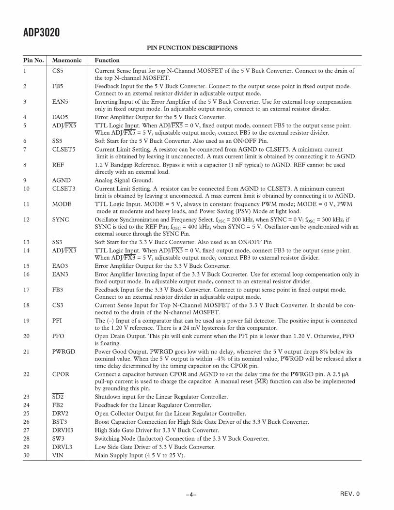
PIN FUNCTION DESCRIPTIONS
Pin No. Mnemonic Function
1 CS5 Current Sense Input for top N-Channel MOSFET of the 5 V Buck Converter. Connect to the drain ofthe top N-channel MOSFET.
2 FB5 Feedback Input for the 5 V Buck Converter. Connect to the output sense point in fixed output mode.Connect to an external resistor divider in adjustable output mode.
3 EAN5 Inverting Input of the Error Amplifier of the 5 V Buck Converter. Use for external loop compensationonly in fixed output mode. In adjustable output mode, connect to an external resistor divider.
4 EAO5 Error Amplifier Output for the 5 V Buck Converter.5 ADJ/FX5 TTL Logic Input. When ADJ/FX5 = 0 V, fixed output mode, connect FB5 to the output sense point.
When ADJ/FX5 = 5 V, adjustable output mode, connect FB5 to the external resistor divider.6 SS5 Soft Start for the 5 V Buck Converter. Also used as an ON/OFF Pin.7 CLSET5 Current Limit Setting. A resistor can be connected from AGND to CLSET5. A minimum current
limit is obtained by leaving it unconnected. A max current limit is obtained by connecting it to AGND.8 REF 1.2 V Bandgap Reference. Bypass it with a capacitor (1 nF typical) to AGND. REF cannot be used
directly with an external load.9 AGND Analog Signal Ground.10 CLSET3 Current Limit Setting. A resistor can be connected from AGND to CLSET3. A minimum current
limit is obtained by leaving it unconnected. A max current limit is obtained by connecting it to AGND.11 MODE TTL Logic Input. MODE = 5 V, always in constant frequency PWM mode; MODE = 0 V, PWM
mode at moderate and heavy loads, and Power Saving (PSV) Mode at light load.12 SYNC Oscillator Synchronization and Frequency Select. fOSC = 200 kHz, when SYNC = 0 V; fOSC = 300 kHz, if
SYNC is tied to the REF Pin; fOSC = 400 kHz, when SYNC = 5 V. Oscillator can be synchronized with anexternal source through the SYNC Pin.
13 SS3 Soft Start for the 3.3 V Buck Converter. Also used as an ON/OFF Pin14 ADJ/FX3 TTL Logic Input. When ADJ/FX3 = 0 V, fixed output mode, connect FB3 to the output sense point.
When ADJ/FX3 = 5 V, adjustable output mode, connect FB3 to external resistor divider.15 EAO3 Error Amplifier Output for the 3.3 V Buck Converter.16 EAN3 Error Amplifier Inverting Input of the 3.3 V Buck Converter. Use for external loop compensation only in
fixed output mode. In adjustable output mode, connect to an external resistor divider.17 FB3 Feedback Input for the 3.3 V Buck Converter. Connect to output sense point in fixed output mode.
Connect to an external resistor divider in adjustable output mode.18 CS3 Current Sense Input for Top N-Channel MOSFET of the 3.3 V Buck Converter. It should be con-
nected to the drain of the N-channel MOSFET.19 PFI The (–) Input of a comparator that can be used as a power fail detector. The positive input is connected
to the 1.20 V reference. There is a 24 mV hysteresis for this comparator.20 PFO Open Drain Output. This pin will sink current when the PFI pin is lower than 1.20 V. Otherwise, PFO
is floating.21 PWRGD Power Good Output. PWRGD goes low with no delay, whenever the 5 V output drops 8% below its
nominal value. When the 5 V output is within –4% of its nominal value, PWRGD will be released after atime delay determined by the timing capacitor on the CPOR pin.
22 CPOR Connect a capacitor between CPOR and AGND to set the delay time for the PWRGD pin. A 2.5 µApull-up current is used to charge the capacitor. A manual reset (MR) function can also be implementedby grounding this pin.
23 SD2 Shutdown input for the Linear Regulator Controller.24 FB2 Feedback for the Linear Regulator Controller.25 DRV2 Open Collector Output for the Linear Regulator Controller.26 BST3 Boost Capacitor Connection for High Side Gate Driver of the 3.3 V Buck Converter.27 DRVH3 High Side Gate Driver for 3.3 V Buck Converter.28 SW3 Switching Node (Inductor) Connection of the 3.3 V Buck Converter.29 DRVL3 Low Side Gate Driver of 3.3 V Buck Converter.30 VIN Main Supply Input (4.5 V to 25 V).
ADP3020
–5–REV. 0
CAUTIONESD (electrostatic discharge) sensitive device. Electrostatic charges as high as 4000 V readilyaccumulate on the human body and test equipment and can discharge without detection. Althoughthe ADP3020 features proprietary ESD protection circuitry, permanent damage may occur ondevices subjected to high-energy electrostatic discharges. Therefore, proper ESD precautions arerecommended to avoid performance degradation or loss of functionality.
WARNING!
ESD SENSITIVE DEVICE
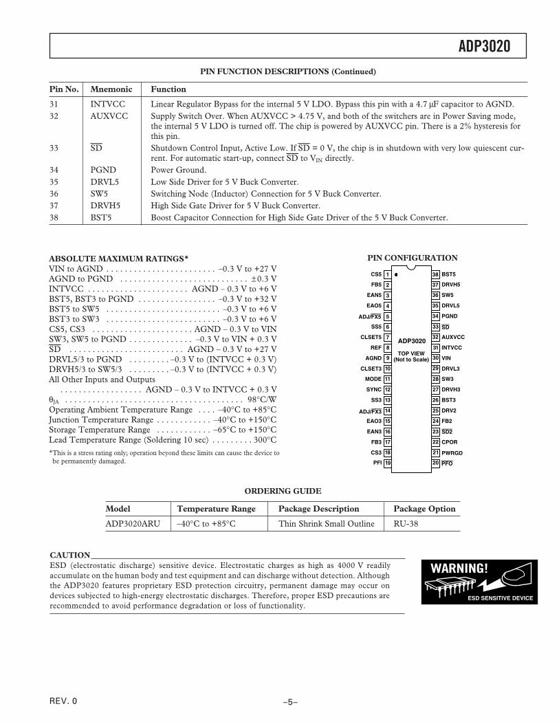
PIN FUNCTION DESCRIPTIONS (Continued)
Pin No. Mnemonic Function
31 INTVCC Linear Regulator Bypass for the internal 5 V LDO. Bypass this pin with a 4.7 µF capacitor to AGND.32 AUXVCC Supply Switch Over. When AUXVCC > 4.75 V, and both of the switchers are in Power Saving mode,
the internal 5 V LDO is turned off. The chip is powered by AUXVCC pin. There is a 2% hysteresis forthis pin.
33 SD Shutdown Control Input, Active Low. If SD = 0 V, the chip is in shutdown with very low quiescent cur-rent. For automatic start-up, connect SD to VIN directly.
34 PGND Power Ground.35 DRVL5 Low Side Driver for 5 V Buck Converter.36 SW5 Switching Node (Inductor) Connection for 5 V Buck Converter.37 DRVH5 High Side Gate Driver for 5 V Buck Converter.38 BST5 Boost Capacitor Connection for High Side Gate Driver of the 5 V Buck Converter.
ABSOLUTE MAXIMUM RATINGS*
VIN to AGND . . . . . . . . . . . . . . . . . . . . . . . . –0.3 V to +27 VAGND to PGND . . . . . . . . . . . . . . . . . . . . . . . . . . . . ±0.3 VINTVCC . . . . . . . . . . . . . . . . . . . . . . AGND – 0.3 V to +6 VBST5, BST3 to PGND . . . . . . . . . . . . . . . . . –0.3 V to +32 VBST5 to SW5 . . . . . . . . . . . . . . . . . . . . . . . . . –0.3 V to +6 VBST3 to SW3 . . . . . . . . . . . . . . . . . . . . . . . . . –0.3 V to +6 VCS5, CS3 . . . . . . . . . . . . . . . . . . . . . . AGND – 0.3 V to VINSW3, SW5 to PGND . . . . . . . . . . . . . . –0.3 V to VIN + 0.3 VSD . . . . . . . . . . . . . . . . . . . . . . . . . AGND – 0.3 V to +27 VDRVL5/3 to PGND . . . . . . . . . –0.3 V to (INTVCC + 0.3 V)DRVH5/3 to SW5/3 . . . . . . . . . –0.3 V to (INTVCC + 0.3 V)All Other Inputs and Outputs
. . . . . . . . . . . . . . . . . . AGND – 0.3 V to INTVCC + 0.3 VθJA . . . . . . . . . . . . . . . . . . . . . . . . . . . . . . . . . . . . . . . 98°C/WOperating Ambient Temperature Range . . . . –40°C to +85°CJunction Temperature Range . . . . . . . . . . . . –40°C to +150°CStorage Temperature Range . . . . . . . . . . . . –65°C to +150°CLead Temperature Range (Soldering 10 sec) . . . . . . . . . 300°C*This is a stress rating only; operation beyond these limits can cause the device to
be permanently damaged.
PIN CONFIGURATION
ORDERING GUIDE
Model Temperature Range Package Description Package Option
ADP3020ARU –40°C to +85°C Thin Shrink Small Outline RU-38
14
13
12
11
10
9
8
1
2
3
4
7
6
5
19
18
17
16
15
20
29
28
27
32
31
30
38
37
36
35
34
33
23
22
21
26
25
24
TOP VIEW(Not to Scale)
ADP3020
BST5
DRVH5
SW5
DRVL5
PGND
SD
AUXVCC
INTVCC
VIN
DRVL3
SW3
DRVH3
BST3
DRV2
FB2
SD2
CPOR
PWRGD
CS5
FB5
EAN5
EAO5
PFI
SS5
CLSET5
REF
AGND
CLSET3
MODE
SYNC
SS3
PFO
EAO3
EAN3
FB3
CS3
ADJ/FX3
ADJ/FX5
ADP3020
–6– REV. 0
CONTROLLOGIC
INTVCC
DRV2
FB2
SD2
CPOR
PWRGD
AGND
SYNC
+– CS5
2.5V
3.3V
1.2V
INTVCC
–3mV
1.22V
Q
R
S
DUPLICATE FOR SECOND CONTROLLER
SHUTDOWN
1.2V
2.5V
ON5
POWER–ON
RESET
SS5
EAO5
EAN5
1.2V
1.2V
1.44V
0.96V
OC
FB5
FB5
DRVL5
SW5 VOUT55V
1.2V
REF
INPUT
5V+5V
LINEAR REG
AUXVCC
CLSET5
BST5
4.7V
DRVH5
VIN
1.2V
200kHz/300kHz/400kHz
OSC
ADJ/FX5
–
+
4A
PGND
0.7A
MODE
14mV
72mVADP3020
SD
1.18V
30
33
32
31
8
9
11
12
21
22
25
24
23
6
5
4
3
37
35
36
38
7
2
1
PFO
PFI
+
–19
1.20V
20
4A
1.2VREF ULVO
+
–
+
–
+
–+2%
+
–
+
–
+
–
–2%
0%
EA
+
–
+
–
+–
34
+
–
+
–+20%
+
––20%
+
–
+
–
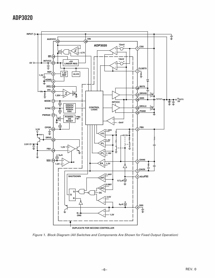
Figure 1. Block Diagram (All Switches and Components Are Shown for Fixed Output Operation)
ADP3020
–7–REV. 0
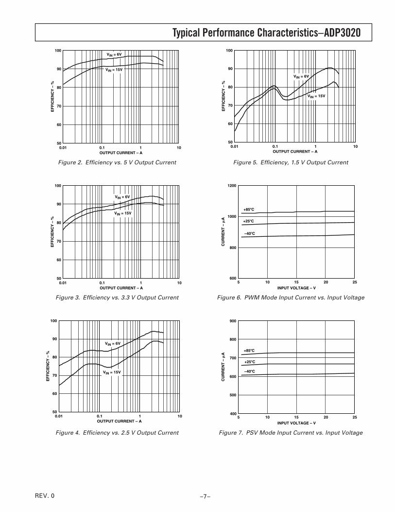
Typical Performance Characteristics–
OUTPUT CURRENT – A
100E
FF
ICIE
NC
Y –
%
90
80
70
60
500.01 0.1 1 10
VIN = 6V
VIN = 15V
Figure 2. Efficiency vs. 5 V Output Current
OUTPUT CURRENT – A
100
EF
FIC
IEN
CY
– %
90
80
70
60
500.01 0.1 1 10
VIN = 6V
VIN = 15V
Figure 3. Efficiency vs. 3.3 V Output Current
OUTPUT CURRENT – A
100
EFF
ICIE
NC
Y –
%
90
80
70
60
500.01 0.1 1 10
VIN = 6V
VIN = 15V
Figure 4. Efficiency vs. 2.5 V Output Current
OUTPUT CURRENT – A
100
EFF
ICIE
NC
Y –
%
90
80
70
60
500.01 0.1 1 10
VIN = 6V
VIN = 15V
Figure 5. Efficiency, 1.5 V Output Current
INPUT VOLTAGE – V
5
CU
RR
EN
T –
A
10 15 20
800
1000
1200
60025
+85C
+25C
–40C
Figure 6. PWM Mode Input Current vs. Input Voltage
INPUT VOLTAGE – V
5
CU
RR
EN
T –
A
10 15 20
900
40025
800
700
600
500
+85C
+25C
–40C
Figure 7. PSV Mode Input Current vs. Input Voltage
ADP3020
–8– REV. 0
INPUT VOLTAGE – V
5
CU
RR
EN
T –
A
10 15 20
200
250
300
10025
150
+25C
–40C
+85C
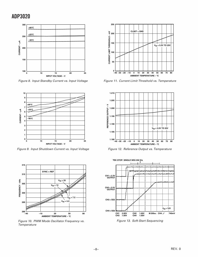
Figure 8. Input Standby Current vs. Input Voltage
INPUT VOLTAGE – V
5
CU
RR
EN
T –
A
10 15 20
2
3
10
025
+25C
–40C
1
+85C
6
7
4
5
8
9
Figure 9. Input Shutdown Current vs. Input Voltage
AMBIENT TEMPERATURE – C–40
FR
EQ
UE
NC
Y –
kH
z
–10 20 50
295
315
290
305
300
310
80
SYNC = REF
VIN = 25
VIN = 12
VIN = 7.5
VIN = 5.5
Figure 10. PWM Mode Oscillator Frequency vs.Temperature
AMBIENT TEMPERATURE – C
–40
CU
RR
EN
T L
IMIT
TH
RE
SH
OL
D –
mV
–30 –20 –10
50
250
0
150
100
200
VIN = 5.5V TO 25V
CLSET = GND
0 10 20 30 40 50 60 70 80
Figure 11. Current Limit Threshold vs. Temperature
AMBIENT TEMPERATURE – C
–40
RE
FE
RE
NC
E O
UT
PU
T –
V
–30 –20 –101.180
1.210
1.190
1.185
1.195
0 10 20 30 40 50 60 70 80
1.200
1.205
VIN = 5.5V TO 25V
Figure 12. Reference Output vs. Temperature
CH1 = 3.3VOUTPUT
CH2 = 2.5VOUTPUT
CH3 = SS3
CH4 = SS5
T[ ]
CH1 2.00V CH2 1.00V M 200MS CH4 740mVCH3 1.00V CH4 1.00V
VIN = 12V
TEK STOP: SINGLE SEQ 250 S/s
Figure 13. Soft-Start Sequencing
ADP3020
–9–REV. 0
CH1 = 5VOUTPUT
CH2 = I OUT =10mA TO 3A
T[ ]
CH1 200mV CH2 2.00V M 200s CH2 1.88V
STOP
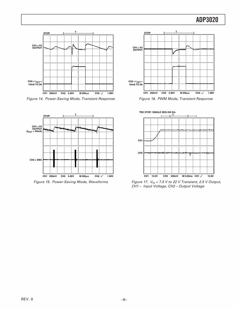
Figure 14. Power-Saving Mode, Transient Response
T[ ]
CH1 200mV CH2 5.00V M 400s CH2 1.90V
CH1 = 5VOUTPUT
(IOUT = 20mA)
CH2 = SW5
STOP
Figure 15. Power-Saving Mode, Waveforms
CH1 = 5VOUTPUT
CH2 = I OUT =10mA TO 3A
T[ ]
CH1 200mV CH2 2.00V M 200s CH2 1.88V
STOP
Figure 16. PWM Mode, Transient Response
CH1
CH2
T[ ]
CH1 10.0V CH2 200mV M 5.00ms CH1 10.8V
TEK STOP: SINGLE SEQ 250 S/s
Figure 17. VIN = 7.5 V to 22 V Transient, 2.5 V Output, CH1 – Input Voltage, CH2 – Output Voltage
ADP3020
–10– REV. 0
THEORY OF OPERATIONThe ADP3020 is a dual-mode, step-down power supply controllerfor notebook computers or similar battery-powered applications.The device contains two synchronous step-down buck control-lers and a linear regulator controller. The buck controllers in theADP3020 have the ability to provide either fixed 3.3 V and 5 Voutputs or independently adjustable (1.25 V to VIN–0.5 V) out-puts. High efficiency over a broad load range is achieved by using aproprietary dual-mode PWM/power-saving (PSV) mode architec-ture. Efficiency is further improved by deleting the external currentsense resistor, which is the main contributor to loss during highcurrent, low output voltage conditions.
CIRCUIT DESCRIPTIONDual-Mode ArchitectureThe ADP3020 contains two independent dual-mode, synchro-nous buck controllers. Traditional constant frequency PWMbuck converters suffer from relatively low efficiency under lightload conditions. In order to maintain high efficiency over a wideload range, the ADP3020 uses a proprietary dual-mode archi-tecture. At moderate to heavy loads, the buck converter operatesin the traditional Pulsewidth Modulation (PWM) mode. At lightloads, PSV mode is used to increase system efficiency. A propri-etary detection scheme is used for transition from one mode to theother. Input current to the high-side MOSFET is detected whengoing from PWM mode to PSV mode, and output voltage infor-mation is used when changing from PSV mode to PWM mode.
When the high-side N-channel MOSFET is turned on, the currentgoing through the N-channel MOSFET is measured as a voltagebetween CS and SW. If the peak current through the MOSFETis less than 20% of the current limit value set by CLSET, aninternal counter that is based on the oscillator frequency will bestarted. If the current stays below this threshold for 16 PWMcycles, the buck converter will enter power-saving mode. Thecounter will automatically reset if the peak current is higher than20% of the current limit value any time prior to when the counterreaches 16.
In PSV mode, the buck converter works like a window regula-tor. If the output voltage drops below the PWM mode nominaloutput voltage, the high-side MOSFET will be turned on. It willremain on until the output capacitors are charged up to 2%above the PWM mode nominal output voltage. The high-sideMOSFET will then be latched off until the output capacitors aredischarged to the lower threshold. The discharge rate is depen-dent on the output capacitor value and load current.
It is important to note that the current limit threshold when inPSV mode is approximately 1/4 of the current limit thresholdwhen in PWM mode. If a large load is applied to the converterwhen in PSV mode (for example, larger than the current limit inPSV mode), the output will continue to drop due to the lowercurrent limit threshold of PSV mode. When the output voltagedrops to 2% below the PWM mode nominal voltage, the converterwill automatically return to PWM mode. Once in PWM mode,the current limit is quadrupled, and the output will be chargedup to the nominal level, as long as the load does not exceed thehigher PWM current limit.
PWM/PSV Operation (MODE)Table I shows the summary of the operating modes of the synchro-nous buck controllers. The MODE pin determines whether or notthe controllers remain in PWM mode under all load conditions.
MODE can be driven by an external TTL logic signal. WhenMODE is pulled HIGH, PSV mode operation is disabled, andthe system is always in constant frequency PWM mode. In orderto enable PSV mode at light loads, the MODE pin needs to bepulled LOW.
Table I. PWM Mode and PSV Mode
Load OperatingMode Current Mode Description
High X PWM Constant-Frequency PWMLow Heavy PWM Constant-Frequency PWMLow Moderate PWM Constant-Frequency PWMLow Light PSV Variable-Frequency, Burst
Mode
X = Don’t Care.
Forcing the ADP3020 to always remain in constant frequencyPWM mode can be used to reduce interference, as this allowsfiltering of the fixed fundamental frequency and its harmonics.The operating frequency should be carefully chosen so that boththe fundamental and harmonic frequencies are not within sensitiveaudio or IF bands. This is particularly important in noise-sensitiveapplications such as multimedia systems, cellular phones, com-puters with built-in RF communications, and PDAs. If two ormore switching regulators are used in a system, it is best to syn-chronize all the switching regulators to a single master regulatoror an external clock signal.
Internal 5 V Supply (INTVCC)An internal low dropout regulator (LDO) generates a 5 V supply(INTVCC) that powers all of the functional blocks within theIC. The total current rating of this LDO is 50 mA. However,this current is used for supplying gate-drive power, and it is notrecommended that current be drawn from this pin for otherpurposes. Bypass INTVCC to AGND with a 4.7 µF capacitor.A UVLO circuit is also included in the regulator. When INTVCC< 3.8 V, the two switching regulators and the linear regulatorcontroller are shut down. The UVLO hysteresis voltage is about120 mV. The internal LDO has a built-in fold-back currentlimit, so that it will be protected if a short circuit is applied tothe 5 V output.
If AUXVCC is higher than 4.75 V, and both the 5 V and 3.3 Vswitching regulators are in PSV mode, an internal switch willconnect INTVCC to AUXVCC, while simultaneously turningoff the internal LDO. AUXVCC can be tied to either the 5 Vswitching regulator output or a separate 5 V voltage source. Bydoing this, the power loss across the internal LDO is eliminated,and the total efficiency in PSV mode is improved.
When AUXVCC = GND, this automatic power switchover fea-ture will be disabled.
Internal Reference (REF)The ADP3020 contains a precision 1.2 V bandgap reference.Bypass REF to AGND with a 1 nF ceramic capacitor. The ref-erence is intended for internal use only. An external voltagebuffer is needed if the reference is used for another purpose.
Boost High Side Gate Drive Supply (BST)The gate drive voltage for the high-side N-channel MOSFETs isgenerated by a flying-capacitor boost circuit. The boost capacitorconnected between BST and SW is charged from the INTVCCsupply. Use only small-signal diodes for the boost circuit.
ADP3020
–11–REV. 0
Synchronous Rectifier (DRVL)Synchronous rectification is used to reduce conduction lossesand to ensure proper start-up of the boost gate driver circuit.Antishoot-through protection has been included to prevent crossconduction during switch transitions. The low side driver mustbe turned off before the high side driver is turned on. For typi-cal N-channel MOSFETs, the dead time is about 50 ns. On theother edge, a dead time of about 50 ns is achieved by an internaldelay circuit. The synchronous rectifier is turned off when thecurrent flowing through the low-side MOSFET falls to zero whenin Discontinuous Conduction (DCM) PWM mode and PSV mode.In Continuous Conduction (CCM) PWM mode, the currentflowing through the low-side MOSFET never reaches zero, so thesynchronous rectifier is turned off by the next clock cycle.
Oscillator Frequency and Synchronization (SYNC)The SYNC pin controls the oscillator frequency. When SYNC= 0 V, fOSC = 200 kHz ; when SYNC = REF, fOSC = 300 kHz;when SYNC = 5 V, fOSC = 400 kHz. 400 kHz operation willminimize external component size and cost while 200 kHz opera-tion provides better efficiency and lower dropout. The SYNCpin can also be used to synchronize the oscillator with an exter-nal 5 V clock signal. A low-to-high transition on SYNC initiatesa new cycle. Synchronization range is 230 kHz to 600 kHz.
Shutdown (SD)Holding SD = GND low will put the ADP3020 into ultralowcurrent shutdown mode. For automatic start-up, SD can be tieddirectly to VIN.
Soft-Start and Power-Up Sequencing (SS)SS3 and SS5 are soft start pins for the two controllers. A 4 µApull-up current is used to charge an external soft start capacitor.Power-up sequencing can be easily done by choosing differentsize external capacitors. When SS3/SS5 < 1.2 V, the two switch-ing regulators are turned off. When 1.2 V < SS5/SS3 < 2.6 V,the regulators start working in soft start mode. When SS3/SS5 >2.6 V, the regulators are in normal operating mode. The con-trollers are forced to stay in PWM mode during the soft-startperiod. The minimum soft-start time (~20 µs) is set by an inter-nal capacitor. Table II shows the ADP3020 operating modes.
Current Limiting (CLSET)A cycle-by-cycle current limiting scheme is used by monitoringcurrent through the top N-channel MOSFET when it is turnedon. By measuring the voltage drop across the high-side MOSFETVDS(ON), the external sense resistor can be deleted. The currentlimit value can be set by CLSET. When CLSET = Floating, themaximum VDS(ON) = 72 mV at room temperature; when CLSET= 0 V, the maximum VDS(ON) = 144 mV at room temperature. Anexternal resistor can be connected between CLSET and AGNDto choose a value between 72 mV and 144 mV. The temperature
coefficient of RDS(ON) of the N-channel MOSFET is canceled bythe internal current limit circuitry, so that an accurate currentlimit value can be obtained over a wide temperature range. InPSV mode, the current limit value is reduced to about 1/4 ofthe value in PWM mode to reduce the interference noise to othercomponents on the PC board.
Output Undervoltage ProtectionEach switching controller has an undervoltage protection circuit.When the current flowing through the high-side MOSFETreaches the current limit continuously for eight clock cycles,and the output voltage is below 20% of the nominal outputvoltage, both controllers will be latched off and will not restartuntil SD or SS3/SS5 is toggled, or until VIN is cycled below 4 V.This feature is disabled during soft start.
Output Overvoltage ProtectionBoth converter outputs are continuously monitored for overvolt-age. If either output voltage is higher than the nominal outputvoltage by more than 20%, both converter’s high-side gate drivers(DRVH5/3) will be latched off, and the low-side gate driverswill be latched on, and will not restart until SD or SS5/SS3 aretoggled, or until VIN is cycled below 4 V. The low-side gatedriver (DRVL) is kept high when the controller is in off-stateand the output voltage is less than 93% of the nominal outputvoltage. Discharging the output capacitors through the maininductor and low-side N-channel MOSFET will cause the out-put to ring. This will make the output momentarily go belowGND. To prevent damage to the circuit, use a reverse-biased1 A Schottky diode across the output capacitors to clamp thenegative surge.
Power Good Output (PWRGD)The ADP3020 also provides a PWRGD signal for the micropro-cessor. During start-up, the PWRGD pin is held low until 5 Voutput is within –4% of its preset voltage. Then, after a timedelay determined by an external timing capacitor connected fromCPOR to GND, PWRGD will be actively pulled up to INTVCCby an external pull-up resistor. CPOR can also be used as amanual reset (MR) function. When the 5 V output is lower thanthe preset voltage by more than 8%, PWRGD is immediatelypulled low.
Linear Regulator ControllerThe ADP3020 includes an onboard linear regulator controller.An external PNP transistor can be used for operation up to 1 A.For higher output current applications, a low threshold PMOScan be used as the pass transistor. The output voltage can be setby a resistor divider. The minimum output voltage of the LDOis 1.25 V, while the maximum output voltage depends on wherethe LDO input is connected and the dropout voltage of theexternal pass transistor.
Table II. Operating Modes
SD SS5 SS3 Mode Description
Low X X Shutdown All Circuits Turned OffHigh SS5 < 1.2 V SS3 < 1.2 V Standby 5 V and 3.3 V Off; INTVCC = 5 V, REF = 1.2 VHigh 1.2 V < SS5 < 2.6 V X Run 5 V in Soft StartHigh 2.6 V < SS5 X Run 5 V in Normal OperationHigh X 1.2 V < SS3 < 2.6 V Run 3.3 V in Soft StartHigh X 2.6 V < SS3 Run 3.3 V in Normal Operation
ADP3020
–12– REV. 0
Output Voltage AdjustmentFixed output voltages (5 V and 3.3 V) are selected whenADJ/FX5 = ADJ/FX3 = 0 V. The output voltage of each con-troller can also be set by an external feedback resistor networkwhen ADJ/FX5 = ADJ/FX3 = 5 V as shown in Figure 18. Thereshould be two external feedback resistor dividers for each con-troller, one for the voltage feedback loop, and one for outputvoltage monitor. Both resistor dividers need to be identical. Theminimum output voltage is 1.25 V. The maximum output volt-age is limited only by the minimum supply voltage. Remoteoutput voltage sensing can be done for both fixed and adjustableoutput voltage modes.
The output voltage can be calculated using the following formula:
V REF
RR
OUT = × +
112 (1)
where REF = 1.2 V, and R1/R2 = R3/R4.
ADP3020
DRVH
DRVL
FB
ADJ/FX
VIN
5VEAN
R1
R2
R3
R4
VOUT
Figure 18. Adjustable Output Mode
If the loop is carefully compensated, R3 and R4 can be, removed,and FB and EAN can be tied together.
APPLICATION INFORMATIONA typical notebook PC application circuit using the ADP3020 isshown in Figure 19. Although the component values given inFigure 19 are based on a 5 V @ 4 A /3.3 V @ 4 A/2.5 V @ 1.5 Adesign, the ADP3020 output drivers are capable of handling out-put currents anywhere from <1 A to over 10 A. Throughout thissection, design examples and component values will be given forthree different power levels. For simplicity, these levels will bereferred to as low power, basic, and extended power. TableIII shows the input/output specifications for these three levels.
Table III. Typical Power Level Examples
ExtendedLow Power Basic Power
Input VoltageRange 5.5 V to 25 V 5.5 V to 25 V 5.5 V to 25 V
SwitchingOutput 1 3.3 V/2 A 3.3 V/4 A 3.3 V/10 A
SwitchingOutput 2 5 V/2 A 5 V/4 A 5 V/10 A
Linear Output 2.5 V/1 A 2.5 V/1.5 A 2.5 V/2 A
Input Voltage RangeThe input voltage range of the ADP3020 is 5.5 V to 25 V when5 V output is desired, and 4.5 V to 25 V when neither switcheroutput is >4.0 V. This converter design is optimized to deliverthe best performance within a 7.5 V to 18 V range, which is thenominal voltage for three to four cell Li-Ion battery stacks. Volt-ages above 18 V may occur under light loads and when thesystem is powered from an ac adapter with no battery installed.
Maximum Output Current and MOSFET SelectionThe maximum output current for each switching regulator is lim-ited by sensing the voltage drop between the drain and source ofthe high-side MOSFET when it is turned on. A current sensecomparator senses voltage drop between CS5 and SW5 for the5 V converter and between CS3 and SW3 for the 3.3 V converter.The sense comparator threshold is 72 mV when the program-ming pin, CLSET, is floating, and is 144 mV when CLSET isconnected to ground. Current-limiting is based on sensing thepeak current. Peak current varies with input voltage and dependson the inductor value. The higher the ripple current or inputvoltage, the lower the converter maximum output current at theset current sense amplifier threshold. The relation between peakand dc output current is given by:
I I V
V Vf L V
PEAK OUT OUTIN MAX OUT
IN MAX= + ×
× × ×
( )
( )
–2 (2)
At a given current comparator threshold VTH and MOSFETRDS(ON), the maximum inductor peak current is:
I
VR
PEAKTH
DS ON=
( )(3)
Rearranging Equation 2 to solve for IOUT(MAX) gives:
I
VR
VV V
f L VOUT MAX
TH
DS ONOUT
IN MAX OUT
IN MAX( )
( )
( )
( )–
–= ×
× × ×
2 (4)
Normally, VTH should be set to its maximum value of 144 mV.For example, in the circuit of Figure 19, an Si4410, which hasan RDS(ON) of 13.5 mΩ would have a maximum peak currentlimit of around 10 A. A less efficient way to achieve maximumpower from the converter is to design the inductor with a largerinductance, (i.e., a lower ripple current). This helps reducethe peak-to-dc current ratio and increases maximum converteroutput, but may also increase the inductor value and its size.It is important to remember that this current limit circuit isdesigned to protect against high current or short circuit condi-tions only. This will protect the IC and MOSFETs long enoughto allow the output undervoltage protection circuitry to latch offthe supply.
ADP3020
–13–REV. 0
C14A10F
C14B10F
D210BQ040
L26.8H
R2130k
38
37
36
35
34
33
32
31
30
29
28
27
26
25
24
23
22
21
20
CS5
FB5
EAN5
EAO5
ADJ/FX5
SS5
CLSET5
BST5
DRVH5
SW5
DRVL5
PGND
SD
AUXVCC
INTVCC
VIN
DRVL3
SW3
DRVH3
BST3
DRV2
FB2
SD2
CPOR
PWRGD
PFO
REF
AGND
CLSET3
MODE
SYNC
SS3
ADJ/FX3
EAO3
EAN3
FB3
CS3
PFI
U1ADP3020
C168pF
R1010k
C18150pF
C41F
R116.2k
C19330pF
D61N4148
C17100nF
Q5SI4410
Q4SI4410
C161F
R610
1
2
3
4
5
6
7
8
9
10
11
12
13
14
15
16
17
18
19
D410BQ040(OPTIONAL)
C27A68F
C27B68F
VOUT55V, 4A+ +
D310BQ040(OPTIONAL)
C24A68F
C24B68F
VOUT333.3V, 4A+ +
Q2SI4410
Q5SI4410
100nF
C154.7F
C131F
C20A10F
C20B10F
D110BQ040
L16.8H
C264.7F
VOUT252.5V, 1.5A
R947k
C281F
R171k
R813k
R712k
C1133F
R24210k
R2660.4k
C12
R1210k
R1310k
PWRGD
PFO
R144.7
C224.7F
VIN5.5V-25V
R247k
R347k
C51nF
R475k
C8470pF
C968pF
C61F
D51N4148
R510
C2330pF
Q1IRF7404
Figure 19. 45 W, Triple Output DC-DC Converter
ADP3020
–14– REV. 0
Nominal Inductor ValueThe inductor design is based on the assumption that the induc-tor ripple current is 30% of the maximum output dc current atnominal 12 V input voltage. The inductor ripple current andinductance value are not critical, but this choice is quite impor-tant in analyzing the trade-offs between cost, size, efficiency,and volume. The higher the ripple current, the lower the induc-tor size and volume. However, this will lead to higher ac lossesin the windings. Conversely, a higher inductor value meanslower ripple current and smaller output filter capacitors, buttransient response will be slower.
The design of the inductor should be based on the maximumoutput current plus 15% (1/2 of the 30% ripple allowance) atthe nominal input voltage:
L V V
VV I f
IN NOM OUTOUT
IN NOM OUT≥ × ( ) ×
× ×3 ( )
( )– (5)
Optimum standard inductor values for the three power levels areshown in Table IV.
Table IV. Standard Inductor Values
Freq. 3.3 V/2 A 3.3 V/4 A 3.3 V/10 A 5 V/2 A 5 V/4 A 5 V/10 A
200 kHz 20 µH 8.2 µH 3.3 µH 22 µH 10 µH 4.7 µH300 kHz 12 µH 6.8 µH 2.2 µH 15 µH 8.2 µH 3.3 µH400 kHz 10 µH 4.7 µH 1.5 µH 10 µH 6.8 µH 2.2 µH
Inductor SelectionOnce the value for the inductor is known, there are two ways toproceed; either to design the inductor in-house or to buy theclosest inductor that meets the overall design goals.
Standard InductorsBuying a standard inductor will provide the fastest, easiest solu-tion, and many companies offer suitable power inductor solutions.A list of power inductor manufacturers is given in Table V.
DESIGNING THE INDUCTOR IN-HOUSECore Material ConcernsThere are several good choices for low core loss materials athigh frequency. Two examples are distributed gap Kool Mupowdered cores from Magnetics and soft ferrite cores, material3F3, 3F4, 3D3, or 4C4, from Philips. To minimize the ac coreloss, especially when the inductor value is relatively low andripple current is high, the use of low frequency powdered ironcores and low frequency ferrite cores (specified for frequency upto 100 kHz) should be avoided. The ripple current is a key fac-tor for optimization of the converter design and determines corelosses to a large extent. Selecting a high ripple current meansa relatively low inductor value. This, for a given core size,reflects a lower number of turns and higher core loss.
Core GeometryThere are two main categories of ferromagnetic cores that couldbe used in this type of application. Open magnetic loop typessuch as beads, beads on leads, rods, and slugs provide the low-est cost, but do not have focused magnetic fields in the core.The radiated EMI distributed around the magnetic field maycreate problems with noise interference in electronic circuitssurrounding the choke. Other types are cores with closed mag-netic paths, such as pot cores, PQ, U, and E cores, toroids, etc.The cost of these cores is higher, but EMI and RFI performanceis better. A good compromise between price and performanceare cores with a toroidal shape, used primarily in through-holeprinting board designs. A very cost-effective solution based, noton closed-loop core, but on good shielded open-loop core, aresurface-mount power inductors, DO, DT, and DS Series fromCoilcraft.
Table V. Recommended Inductor Manufacturers
Murata ElectronicsCoilcraft Coiltronics North America Inc.
Phone: 847/639-6400 Phone: 561/241-7876 Phone: 770/436-1300Fax: 847/639-1469 Fax: 561/241-9339 Fax: 770/436-3030Web: www.coilcraft.com Web: www.coiltronics.com Web: www.murata.com
SMT Power Inductors, SMT Power Inductors, SMT Power Inductors,Series 1608, 3308, 3316, 5022, 5022HC, Series UNI-PAC2, UNI-PAC3 and UNI-PAC4, Series LQT2535DO3340, Low Cost Solution Low Cost Solution Best for Low EMI/RFISMT Shielded Power Inductors, SMT Power Inductors,Series DS5022, DS3316, DT3316, Series, ECONO-PAC, VERSA-PAC,Best for Low EMI/RFI Best for Low Profile or Flexible Design.
Power Inductors and Chokes, Power Inductors CTX Series, Chip InductorsSeries DC1012, PCV-0, PCV-1, PCV-2, Low EMI/RFI, Low Cost Toroidal Inductors LQN6C, LQS66CPCH-27, PCH-45, Low Cost but Not Miniature.
ADP3020
–15–REV. 0
The DesignThe details of designing the power inductor are covered in manyreference texts, and will not be covered here. Examples of soft-ware and reference books that can be used for quick design ofthe power inductor are given below:
Software—Magnetic Designer from Intusoft, www.intusoft.com
“Designing Magnetic Components for High FrequencyDC-DC Converters,” McLyman, Kg Magnetics Inc.,ISBN 1-883107-00-08 (for advanced users)
“Power Supply Cookbook,” Marty Brown, EDN Series forDesign Engineers, ISBN 0-7506-9442-4 (for beginners andintermediate users)
CIN and COUT SelectionIn continuous conduction mode, the source current of the upperMOSFET is approximately a square wave of duty cycle VOUT/VIN.To prevent large voltage transients, a low ESR input capacitorsized for the maximum rms current must be used. The maximumrms capacitor current is given by:
I V V V
IV
RMS OUT IN OUTMAX
IN≈ × ( ) ×– (6)
This formula has a maximum at VIN = 2 × VOUT, where IRMS =IOUT/2. Note that the capacitor manufacturer’s ripple currentratings are often based on only 2000 hours of life. This makes itadvisable to further derate the capacitor, or to choose a capacitorrated at a higher temperature than required. Several capacitorsmay also be paralleled to meet size or height requirements in thedesign. If electrolytic or tantalum capacitors are used, an addi-tional 0.1 µF–1 µF ceramic bypass capacitor should be placed inparallel with CIN.
The selection of COUT is driven by the required effective seriesresistance (ESR) and the desired output ripple. A good rule ofthumb is to limit the ripple voltage to 1% of the nominal outputvoltage. It is assumed that the total ripple is caused by two factors:25% comes from the COUT bulk capacitance value, and 75%comes from the capacitor ESR. The value of COUT can be deter-mined by:
C
If V
OUTRIPPLE
RIPPLE=
× ×2 (7)
where IRIPPLE = 0.3 × IOUT and VRIPPLE = 0.01 × VOUT. Themaximum acceptable ESR of COUT can then be found using:
ESR
VI
RIPPLE
RIPPLE
≤ ×0 75. (8)
Manufacturers such as Vishay, AVX, Elna, WIMA and Sanyoprovide good high-performance capacitors. Sanyo’s OSCONsemiconductor dielectric capacitors have lower ESR for a givensize, at a somewhat higher price. Choosing sufficient capacitorsto meet the ESR requirement for COUT will normally exceedthe amount of capacitance needed to meet the ripple currentrequirement.
In surface-mount applications, multiple capacitors may have tobe paralleled to meet the capacitance, ESR, or RMS currenthandling requirements. Aluminum electrolytic and dry tantalumcapacitors are available in surface-mount configurations. In thecase of tantalum, it is critical that capacitors are surge tested foruse in switching power supplies. Recommendations for outputcapacitors are shown in Table VI.
Power MOSFET SelectionN-channel power MOSFETs must be selected for use with theADP3020 for both the main and synchronous switch. The mainselection parameters for the power MOSFETs are the thresholdvoltage (VGS(TH)) and ON-resistance (RDS(ON)). An internal LDOgenerates a 5 V supply that is boosted above the input voltageusing a bootstrap circuit. This floating 5 V supply is used for theupper MOSFET gate drive. Logic-level threshold MOSFETsmust be used for both the main and synchronous switches.
Maximum output current (IMAX) determines the RDS(ON) require-ment for the two power MOSFETs. When the ADP3020 isoperating in continuous mode, the simplifying assumption canbe made that one of the two MOSFETs is always conducting theload current. The duty cycles for the MOSFETs are given by:
Upper MOSFET Duty Cycle
VV
OUT
IN= (9)
Lower MOSFET Duty Cycle
V VV
IN OUT
IN=
–(10)
Table VI. Recommended Capacitor Manufacturers
Maximum OutputCurrent 2 A 4 A 10 A
Input Capacitors TOKIN Multilayer TOKIN Multilayer TOKIN MultilayerCeramic Caps, 22 µF/25 V Ceramic Caps, 2 × 22 µF/25 V Ceramic Caps, 2 × 22 µF/25 VP/N: C55Y5U1E226Z P/N: C55Y5U1E226Z P/N: C55Y5U1E226ZTAIYO YUDEN INC. TAIYO YUDEN INC. VISHEY Ceramic Caps,Ceramic Caps, Y5V Series Ceramic Caps, Y5V Series Z5U Series, 2 × 15 µF/25 V10 µF/25 V 2 ×10 µF/25 VP/N: TMK432BJ106KM P/N: TMK432BJ106KM
Output Capacitors SANYO POSCAP TPC SANYO POSCAP TPC SANYO POSCAP TPB+3.3 V Output Series, 68 µF/10 V Series, 2 × 68 µF/10 V Series, 2 × 220 µF/4.0 V
Output Capacitors SANYO POSCAP TPC SANYO POSCAP TPC SANYO POSCAP TPB+5 V Output Series, 68 µF/10 V Series, 2 × 68 µF/10 V Series, 2 × 330 µF/6.3 V
ADP3020
–16– REV. 0
From the duty cycle, the required minimum RDS(ON) for eachMOSFET can be derived by the following equations:
Upper MOSFET:
R UpperV P
V I TDS ON
IN D
OUT MAX
( ) ( ) = ×
× × +( )21 α∆ (11)
Lower MOSFET:
R LowerV P
V V I TDS ON
IN D
IN OUT MAX
( ) ( )–
=×
( ) × × +( )21 α∆ (12)
where PD is the allowable power dissipation and α is the tempera-ture dependency of RDS(ON). PD will be determined by efficiencyand/or thermal requirements (see Efficiency ). (1 + α∆T) is gen-erally given for a MOSFET in the form of a normalized RDS(ON)
vs. temperature curve, but α = 0.007/°C can be used as anapproximation for low voltage MOSFETs.
Maximum MOSFET power dissipation occurs at maximumoutput current, and can be calculated as follows:
Upper MOSFET:
P Upper
VV
I R TDOUT
INMAX DS ON( ) ( )( )= × × × +2
1 α∆ (13)
Lower MOSFET:
P Lower
V VV
I R TDIN OUT
INMAX DS ON( )
–( )( )= × × × +21 α∆ (14)
The Schottky diode, D1 shown in Figure 19, conducts only duringthe dead time between conduction of the two power MOSFETs.D1’s purpose is to prevent the body-diode of the lower N-channelMOSFET from turning on and storing charge during the deadtime, which could cost as much as 1% in efficiency. D1 shouldbe selected for forward voltage of less than 0.5 V when conductingIMAX. Recommended transistors for upper and lower MOSFET’sare given in Table VII.
Table VII. Recommended MOSFETs
MaximumOutput 2 A 4 A 10 A
Vishay/ Si4412DY, Si4410DY, Si4874DY,Siliconix 28 mΩ 13.5 mΩ 7.5 mΩ
International IRF7805, IRF7811, IRFBA3803,Rectifier 11 mΩ 8.9 mΩ 5.5 mΩ
IRF7805, IRF7809,11 mΩ 7.5 mΩ
Soft StartThe soft-start time of each of switching regulator can be pro-grammed by connecting a soft-start capacitor to the correspondingsoft-start pin (SS3 or SS5). The time it takes each regulator toramp up to its full duty ratio depends proportionally on thevalues of the soft-start capacitors. The charging current is 4 µA±20%. The capacitor value to set a given soft-start time, tSS, isgiven by:
C A
t
VpFSS
SS≅ µ ×( )
42 6.
( ) (15)
Fixed or Adjustable Output VoltageEach switching controller of the ADP3020 can be programmedto operate with a fixed or adjustable output voltage. As shownby the general application schematic in Figure 19, putting theADP3020 into fixed mode gives a nominal output of 3.3 V and5 V for the two switching buck converters. By using two identi-cal resistor dividers per converter, any output voltage between1.25 V and VIN–0.5 V can be set. The center point of one divideris connected to the feedback pin, FB, and the center point of theother identical divider is connected to EAN. It is important to use1% resistors. A good value for the lower leg resistors is 10 kΩ,1%, then the upper leg resistors for a given output voltage canbe determined by:
R
V VkUPPER
OUT= Ω– ..
( )1 2
0 12(16)
Table VIII shows the resistor values for the most common out-put voltages.
Table VIII. Typical Feedback Resistor Values
VOUT 1.25 V 1.3 V 1.5 V 1.8 V 2.0 V 2.5 V 3.0 V 3.3 V 5.0 V
RUPPER 412 Ω 825 Ω 2.49 kΩ 4.99 kΩ 6.65 kΩ 10.7 kΩ 15.0 kΩ 17.4 kΩ 31.6 kΩRLOWER 10 kΩ 10 kΩ 10 kΩ 10 kΩ 10 kΩ 10 kΩ 10 kΩ 10 kΩ 10 kΩ
ADP3020
–17–REV. 0
PWM Mode/Power-Saving (PSV) Mode OperationThe mode of operation for both switching regulators can be presetusing the MODE pin. When MODE is HIGH, or connected toINTVCC, both converters work only in PWM mode, regardlessof output current. MODE connected to GND makes both con-verters operate in a dual PWM/PSV mode of operation. In dualmode, each converter has its own boundary output current whenthe converter switches from PSV mode to PWM mode and viceversa. There is an output current hysteresis for each mode tran-sition to avoid improper operation.
There are several design recommendations regarding dual modeoperation. The trip output current level for switching betweenPWM mode and PSV mode is a percentage of the peak currentsensed via the internal current sense comparator. However,the value of that current depends on the RDS(ON) of the upperMOSFET. For example, if the design uses an Si4420 versus anSi4410 power MOSFET (9 mΩ vs. 13.5 mΩ) the maximumoutput power of the converter and the mode trip output currentwill both be 50% higher.
Efficiency EnhancementThe efficiency of each switching regulator is inversely propor-tional to the losses during the switching conversion. The mainfactors to consider when attempting to maximize efficiency are:
1. Resistive losses, which include the RDS(ON) of upper andlower MOSFETs, trace resistances and output choke wireresistance.
These losses contribute a major part of the overall power lossin low voltage battery-powered applications. However, tryingto reduce these resistive losses by using multiple MOSFETsand thick traces may tend to lead to lower efficiency and higherprice. This is due to the trade-off between reduced resistiveloss and increased gate drive loss that must be consideredwhen optimizing efficiency.
2. Switching losses due to the limited time of switching transitions.
This occurs due to gate drive losses of both upper and lowerMOSFETs, and switching node capacitive losses, as well asthrough hysteresis and eddy-current losses in power choke.Input and output capacitor ripple current losses should alsobe considered as switching losses. These losses are input-voltage-dependent and can be estimated as follows:
P V I C fSWLOSS IN MAX SN= × × × ×2 5
1 85.
. (17)
where CSN is the overall capacitance of the switching noderelated to loss.
3. Supply current of the switching controller (independent ofthe input current redirected to supply the MOSFETs’ gates).
This is a very small portion of the overall loss, but it doesincrease with input voltage.
Transient Response ConsiderationsBoth stability and regulator loop response can be checked bylooking at the load transient response. Switching regulators takeseveral cycles to respond to a step in output load current. Whena load step occurs, output voltage shifts by an amount equal tothe current step multiplied by the total ESR of the summed outputcapacitor array. Output overshoot or ringing during the recoverytime (in both directions of the current step change) indicates astability problem. The external feedback compensation compo-nents shown in Figure 18 should provide adequatecompensation for most applications.
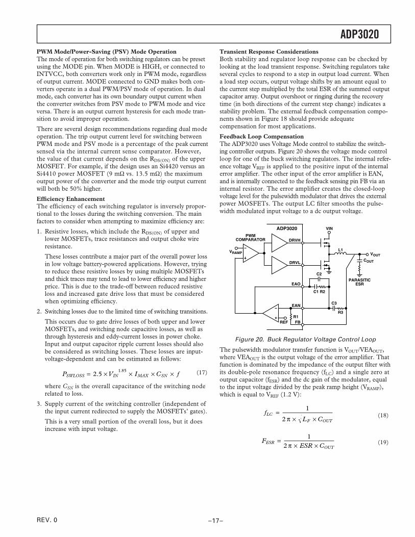
Feedback Loop CompensationThe ADP3020 uses Voltage Mode control to stabilize the switch-ing controller outputs. Figure 20 shows the voltage mode controlloop for one of the buck switching regulators. The internal refer-ence voltage VREF is applied to the positive input of the internalerror amplifier. The other input of the error amplifier is EAN,and is internally connected to the feedback sensing pin FB via aninternal resistor. The error amplifier creates the closed-loopvoltage level for the pulsewidth modulator that drives the externalpower MOSFETs. The output LC filter smooths the pulse-width modulated input voltage to a dc output voltage.
VOUT
COUT
L1
PWMCOMPARATOR
ADP3020 VIN
DRVH
DRVL
PARASITICESREAO
EAN
REFR1
R3
C1
C2
C3
R2
FB
VRAMP
Figure 20. Buck Regulator Voltage Control Loop
The pulsewidth modulator transfer function is VOUT/VEAOUT,where VEAOUT is the output voltage of the error amplifier. Thatfunction is dominated by the impedance of the output filter withits double-pole resonance frequency (fLC) and a single zero atoutput capacitor (fESR) and the dc gain of the modulator, equalto the input voltage divided by the peak ramp height (VRAMP),which is equal to VREF (1.2 V):
fL C
LC
F OUT
=× ×
1
2 π (18)
F
ESR CESR
OUT=
× ×1
2 π (19)
ADP3020
–18– REV. 0
The compensation network consists of the internal error ampli-fier and two external impedance networks ZIN and ZFB. Once theapplication and the output filter capacitance and ESR are chosen,the specific component values of the external impedance net-works ZIN and ZFB can be determined. There are two designcriteria for achieving stable switching regulator behavior withinthe line and load range. One is the maximum bandwidth of theloop, which affects fast transient response, if needed, and theother is the minimum accepted by the design phase margin.
The phase margin is the difference between the closed-loop phaseand 180 degrees. Recommended phase margin is 45 to 60 degreesfor most applications.
The equations for calculating the compensation Poles and Zerosare:
fR
C CC C
P11
2 21 21 2
=× ×
×+
π (20)
f
R CP2
12 3 3
=× ×π (21)
f
R CZ1
12 2 1
=× ×π (22)
f
R R CZ2
12 1 3 3
=× + ×π ( ) (23)
The value of the internal resistor R1 is 71 kΩ for the 3.3 Vswitching regulator, and 128 kΩ for the 5 V switching regulator.
Compensation Loop Design and Test Method1. Choose the gain (R2/R1) for the desired bandwidth.
2. Place fZ1 20%–30% below fLC.
3. Place fZ2 20%–30% above fLC.
4. Place fP1 at fESR, check the output capacitor for worst-case ESRtolerances.
5. Place fP2 at 40%–60% of oscillator frequency.
6. Estimate phase margins in full frequency range (zero frequencyto zero gain crossing frequency).
7. Apply the designed compensation and test the transientresponse under a moderate step load change (30%–60%) andvarious input voltages. Monitor the output voltage viaoscilloscope. The voltage overshoot or undershoot should bewithin 1%–3% of the nominal output, without ringing andabnormal oscillation.
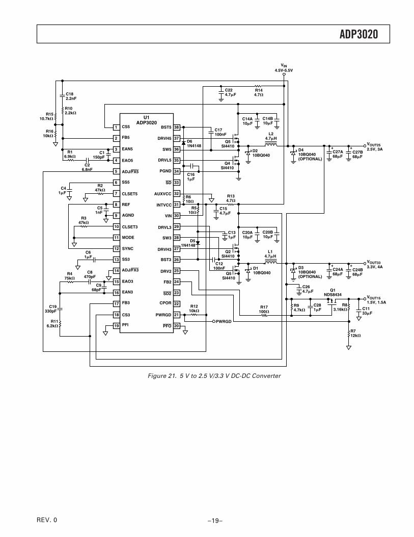
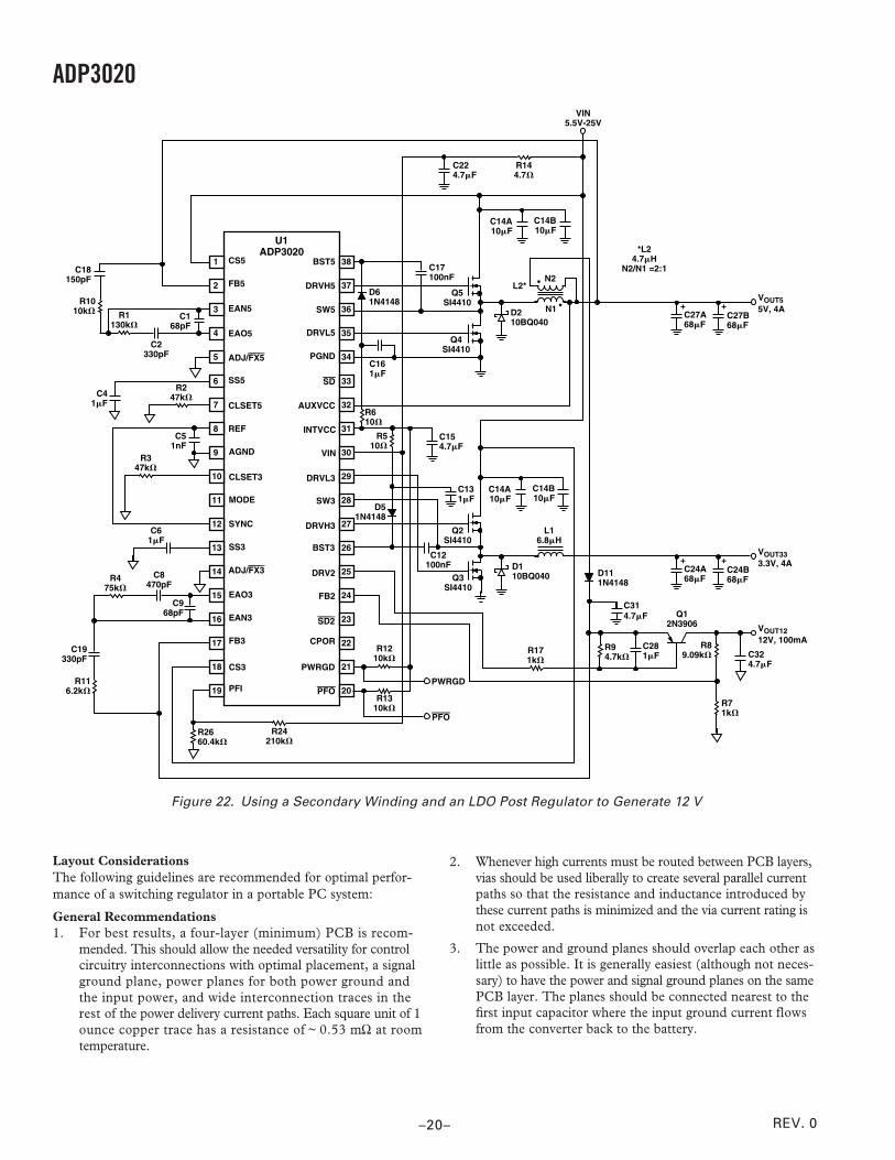
Additional Application CircuitsThe multiple outputs and wide input voltage range of the ADP3020make it a very flexible IC for use in a wide variety of applications.For example, the ADP3020 can be used to generate low voltage(<4.0 V) outputs from a 5 V supply. The circuit shown in Fig-ure 21 converts the 5 V input into a 3.3 V and a 2.5 V output.The circuit of Figure 22 uses a secondary winding on the 5 Voutput to generate an unregulated 15 V rail which is then regu-lated to 12 V by the LDO output of the ADP3020.
ADP3020
–19–REV. 0
C14A10F
C14B10F
D210BQ040
L24.7H
R16.9k
38
37
36
35
34
33
32
31
30
29
28
27
26
25
24
23
22
21
20
CS5
FB5
EAN5
EAO5
ADJ/FX5
SS5
CLSET5
BST5
DRVH5
SW5
DRVL5
PGND
SD
AUXVCC
INTVCC
VIN
DRVL3
SW3
DRVH3
BST3
DRV2
FB2
SD2
CPOR
PWRGD
PFO
REF
AGND
CLSET3
MODE
SYNC
SS3
ADJ/FX3
EAO3
EAN3
FB3
CS3
PFI
U1ADP3020
C1150pF
R1610k
C41F
R116.2k
C19330pF
D61N4148
C17100nF
Q5SI4410
Q4SI4410
C161F
R610
1
2
3
4
5
6
7
8
9
10
11
12
13
14
15
16
17
18
19
D410BQ040(OPTIONAL)
C27A68F
C27B68F
VOUT252.5V, 3A+ +
D310BQ040(OPTIONAL)
C24A68F
C24B68F
VOUT333.3V, 4A+ +
Q2SI4410
Q5SI4410
C154.7F
C131F
C20A10F
C20B10F
D110BQ040
L14.7H
C264.7F
VOUT151.5V, 1.5A
R94.7k
C281F
R17100
R83.16k
R712k
C1133F
C12100nF
R1210k
PWRGD
R144.7
C224.7F
VIN4.5V-5.5V
R247k
R347k
C51nF
R475k
C8470pF
C968pF
C61F
R1510.7k
D51N4148
R510
R102.2k
C182.2nF
R134.7
C26.8nF
Q1NDS8434
Figure 21. 5 V to 2.5 V/3.3 V DC-DC Converter
ADP3020
–20– REV. 0
Layout ConsiderationsThe following guidelines are recommended for optimal perfor-mance of a switching regulator in a portable PC system:
General Recommendations1. For best results, a four-layer (minimum) PCB is recom-
mended. This should allow the needed versatility for controlcircuitry interconnections with optimal placement, a signalground plane, power planes for both power ground andthe input power, and wide interconnection traces in therest of the power delivery current paths. Each square unit of 1ounce copper trace has a resistance of ~ 0.53 mΩ at roomtemperature.
2. Whenever high currents must be routed between PCB layers,vias should be used liberally to create several parallel currentpaths so that the resistance and inductance introduced bythese current paths is minimized and the via current rating isnot exceeded.
3. The power and ground planes should overlap each other aslittle as possible. It is generally easiest (although not neces-sary) to have the power and signal ground planes on the samePCB layer. The planes should be connected nearest to thefirst input capacitor where the input ground current flowsfrom the converter back to the battery.
C14A10F
C14B10F
D210BQ040
L2*
R1130k
38
37
36
35
34
33
32
31
30
29
28
27
26
25
24
23
22
21
20
CS5
FB5
EAN5
EAO5
ADJ/FX5
SS5
CLSET5
BST5
DRVH5
SW5
DRVL5
PGND
SD
AUXVCC
INTVCC
VIN
DRVL3
SW3
DRVH3
BST3
DRV2
FB2
SD2
CPOR
PWRGD
PFO
REF
AGND
CLSET3
MODE
SYNC
SS3
ADJ/FX3
EAO3
EAN3
FB3
CS3
PFI
U1ADP3020
C168pF
R1010k
C18150pF
C41F
R116.2k
C19330pF
D61N4148
C17100nF
Q5SI4410
Q4SI4410
C161F
R610
1
2
3
4
5
6
7
8
9
10
11
12
13
14
15
16
17
18
19
C27A68F
C27B68F
VOUT55V, 4A+ +
C24A68F
C24B68F
VOUT333.3V, 4A+ +
Q2SI4410
Q3SI4410
C154.7F
C131F
C14A10F
C14B10F
D110BQ040
L16.8H
C314.7F
VOUT1212V, 100mA
R94.7k
C281F
R171k
R89.09k
R71k
C324.7F
R24210k
R2660.4k
C12100nF
R1210k
R1310k
PWRGD
PFO
R144.7
C224.7F
VIN5.5V-25V
R247k
R347k
C51nF
R475k
C8470pF
C968pF
C61F
D51N4148
R510
•
•
N2
N1
*L24.7H
N2/N1 =2:1
C2330pF
Q12N3906
D111N4148
Figure 22. Using a Secondary Winding and an LDO Post Regulator to Generate 12 V
ADP3020
–21–REV. 0
4. If critical signal lines (including the voltage and current senselines of the ADP3020) must cross through power circuitry,it is best if a signal ground plane can be interposed betweenthose signal lines and the traces of the power circuitry. Thisserves as a shield to minimize noise injection into the sig-nals at the expense of making signal ground a bit noisier.
5. The PGND pin of the ADP3020 should connect first to aceramic bypass capacitor on the VIN pin, and then into thepower ground plane using the shortest possible trace. How-ever, the power ground plane should not extend under othersignal components, including the ADP3020 itself. If neces-sary, follow the preceding guideline to use the signal plane asa shield between the power ground plane and the signalcircuitry.
6. The AGND pin of the ADP3020 should connect first to theREF capacitor, and then into the signal ground plane. In caseswhere no signal ground plane can be used, short interconnec-tions to other signal ground circuitry in the power convertershould be used.
7. The output capacitors of the power converter should beconnected to the signal ground plane even though powercurrent flows in the ground of these capacitors. For thisreason, it is advised to avoid critical ground connections(e.g., the signal circuitry of the power converter) in the signalground plane between the input and output capacitors. Itis also advised to keep the planar interconnection path short(i.e., have input and output capacitors close together).
8. The output capacitors should also be connected as closelyas possible to the load (or connector) that receives the power.If the load is distributed, the capacitors should also be dis-tributed, and generally in proportion to where the load tendsto be more dynamic.
9. Absolutely avoid crossing any signal lines over the switchingpower path loop, described below.
Power Circuitry10. The switching power path should be routed on the PCB to
encompass the smallest possible area in order to minimizeradiated switching noise energy (i.e., EMI). Failure to takeproper precaution often results in EMI problems for theentire PC system as well as noise-related operational prob-lems in the power converter control circuitry. The switchingpower path is the loop formed by the current path throughthe input capacitors, the two FETs (and the power Schottkydiode if used), including all interconnecting PCB traces andplanes. The use of short and wide interconnection tracesis especially critical in this path for two reasons: it mini-mizes the inductance in the switching loop, which can causehigh-energy ringing, and it accommodates the high currentdemand with minimal voltage loss.
11. A power Schottky diode (1 ~ 2 A dc rating) placed from thelower FET’s source (anode) to drain (cathode) will help tominimize switching power dissipation in the upper FET. Inthe absence of an effective Schottky diode, this dissipationoccurs through the following sequence of switching events.The lower FET turns off in advance of the upper FET turningon (necessary to prevent cross-conduction). The circulatingcurrent in the power converter, no longer finding a path forcurrent through the channel of the lower FET, draws cur-rent through the inherent body-drain diode of the FET.The upper FET turns on, and the reverse recovery char-acteristic of the lower FET’s body-drain diode prevents thedrain voltage from being pulled high quickly.
The upper FET then conducts very large current while itmomentarily has a high voltage forced across it, which trans-lates into added power dissipation in the upper FET. TheSchottky diode minimizes this problem by carrying a majorityof the circulating current when the lower FET is turned off,and by virtue of its essentially nonexistent reverse recov-ery time.
12. Whenever a power-dissipating component (e.g., a powerMOSFET) is soldered to a PCB, the liberal use of vias,both directly on the mounting pad and immediately sur-rounding it, is recommended. Two important reasons forthis are: improved current rating through the vias (if it isa current path), and improved thermal performance, espe-cially if the vias are extended to the opposite side of thePCB where a plane can more readily transfer the heat tothe air.
13. The output power path, though not as critical as the switch-ing power path, should also be routed to encompass a smallarea. The output power path is formed by the current paththrough the inductor, the output capacitors, and back to theinput capacitors.
14. For best EMI containment, the power ground plane shouldextend fully under all the power components except theoutput capacitors. These are: the input capacitors, the powerMOSFETs and Schottky diode, the inductor, and any snub-bing elements that might be added to dampen ringing. Avoidextending the power ground under any other circuitry orsignal lines, including the voltage and current sense lines.
Signal Circuitry15. The CS and SW traces should be Kelvin-connected to the
upper MOSFET drain and source so that the additionalvoltage drop due to current flow on the PCB at the currentsense comparator connections does not affect the sensedvoltage. It is desirable to have the ADP3020 close to the out-put capacitor bank and not in the output power path, so thatany voltage drop between the output capacitors and theAGND pin is minimized, and voltage regulation is notcompromised.
ADP3020
–22– REV. 0
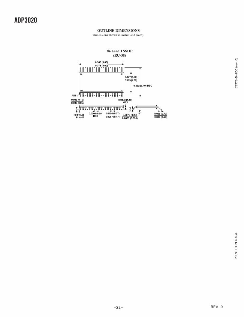
OUTLINE DIMENSIONSDimensions shown in inches and (mm).
38-Lead TSSOP(RU-38)
38 20
191
0.386 (9.80)0.378 (9.60)
0.177 (4.50)0.169 (4.30)
PIN 1
SEATINGPLANE
0.006 (0.15)0.002 (0.05)
0.0200 (0.50)BSC
0.0433 (1.10)MAX
0.0106 (0.27)0.0067 (0.17)
0.0079 (0.20)0.0035 (0.090)
0.028 (0.70)0.020 (0.50)
80
0.252 (6.40) BSC C37
73–5
–4/0
0 (r
ev. 0
)P
RIN
TE
D IN
U.S
.A.