Embed Size (px)
Citation preview

A High Dynamic Range-CMRR and
Tunable Bandwidth Front-End
Amplifier for Biomedical Applications
By
Liliana Haiko Salas Barradas
A Dissertation submitted in partial fulfillment of the requirements
for the degree of:
MASTER ON SCIENCE WITH MAJOR ON
ELECTRONICS
at the
Instituto Nacional de Astrofısica, Optica y Electronica
April 9
Tonantzintla, Puebla
Under the supervision of:
Dr. Alejandro Dıaz Sanchez
Dr. Carlos Muniz Montero
c©INAOE 2015
The author grants to INAOE the permission to reproduce
and distribute parts or complete copies of this thesis
.
“There is a driving force more powerful than steam, electricity
and atomic energy, the will.”
Albert Einstein.

Acknowledgments
First of all, I would like to thank to Consejo Nacional de Ciencia y Tecnologıa (CONA-
CyT) and Programa para el Mejoramiento del Profesorado (PROMEP) by the support
of this work throughout projects 181201 and PROMEP-UPPue-PTC-047
I acknowledge the support given by Instituto Nacional de Astrofısica Optica y Electronica
and all my professors at INAOE during this academic training process.
My special gratitude to my advisors Dr. Alejandro Dıaz Sanchez and Dr. Carlos
Muniz Montero, for their extraordinary support and guidance throughout the develop-
ment of this work.
I am grateful to my parents for giving me all than they are and make me the per-
son who I am, and to my grandparents for their unconditional love all the time.
I would like to thank all my family and all the persons who love me, specially my
aunt and uncle Ofe and Arturo for giving me support in every stage of my life.
Thanks to my angel Harumi and my cousins Sugei, Michelle, Arturo Valeria and Pepito.
Furthermore, I express my gratitude to my Sensei Jaime Ortega for teaching me to
give my best in everything I do in my life with his extraordinary example.
Thanks to my friends and classmates for sharing this experience.
iii
And thanks to you, my love Hector Christian for loving me, believing in me and sup-
porting me in every project of my life.
Finally but not less important, even though they can not read, thanks to my babies
Madara and Canton to come into my life.
Liliana Haiko Salas Barradas

iv
RESUMEN
TITULO:
Amplificador Front-End de Alto Rango Dinamico, Alto CMRR y Ancho de Banda Sin-
tonizable para Aplicaciones Biomedicas
AUTOR:1 Liliana Haiko Salas Barradas
PALABRAS CLAVE: Amplificador Front-End, Senales de Biopotenciales, Filtro
Notch , Preamplificador.
DESCRIPCION: Los desafıos en el diseno de sistemas de monitoreo no invasivos
de biopotenciales, tales como: bajo consumo de potencia, bajo voltaje de alimentacion,
bajo costo y portabilidad, han impulsado a los ingenieros electricos a mejorar el de-
sempeno de dichos sistemas, mas alla de especificaciones usuales para desarrollar apli-
caciones para el cuidado de la salud.
En este trabajo se presenta una propuesta de preamplificador basado en la topologıa
folded cascode combinado con dc-feedback como tecnica de compensacion de offset y una
tecnica feed-forward combinada con transistores Quasi Floating Gates con reutilizacion
de hardware, para mejoramiento de CMRR. Aunado a esto se presentan bloques de
filtrado pasa banda y notch sintonizables para lograr sintonizacion en us frecuencias de
corte de acuerdo a la aplicacion medica requerida (EEG, ECG y EMG). Con el fin de
utilizar este sistema como electrodo activo se busca obtener minimizacion de area en
layout, bajo consumo de potencia y bajo costo en tecnologıa de 0.5µm.
1INAOE, Coordinacion de Electronica. Diseno de circuitos integrados.

v
SUMMARY
TITLE:
A High Dynamic Range-CMRR and Tunnable Bandwidth Front-End Amplifier for
Biomedical Applications
AUTHOR:2 Liliana Haiko Salas Barradas
KEY WORDS: Front-End Amplifier, Biopotential Signals, Notch Filter, Preamplifier.
DESCRIPTION: The challenges in non invasive monitoring systems design for biopo-
tentials acquisition, such as: low power consumption, low supply voltages, low cost and
portability, have encourage electrical engineers to enhance the performance of such sys-
tems, beyond common specifications in order to develop medical care applications.
This work propose a pre-amplifier based on the combination of a folded cascode topol-
ogy, an offset compensation technique based on dc-feedback and a CMRR enhancement
technique based on feed-forward combined with Quasi Floating Gates transistors and
hardware reuse. Additionally, two filter stages, tunable band pass and tunable notch
configurations to achieve tunability in cutoff frequencies according with the required
medical application (EEG,ECG and EMG).
In order to implement this system as an active electrode, the layout area minimiza-
tion, low power consumption and low cost have been pursued in a CMOS technology
of 0.05µm
2INAOE. Electronic Department. Integrated circuit design.

vi
Contents
1 Introduction 1
1.1 Analog preprocessing of biomedical signals . . . . . . . . . . . . . . . . 1
1.2 Preamplifiers Specifications and involved non ideal effects . . . . . . . . 3
1.2.1 Noise Effects . . . . . . . . . . . . . . . . . . . . . . . . . . . . 4
1.2.2 Offset Effects . . . . . . . . . . . . . . . . . . . . . . . . . . . . 4
1.2.3 Offset Stabilization Techniques . . . . . . . . . . . . . . . . . . 5
1.3 State-of-the-Art . . . . . . . . . . . . . . . . . . . . . . . . . . . . . . . 9
1.4 Goals and Description of this work . . . . . . . . . . . . . . . . . . . . 17
2 Theoretical Framework 23
2.1 Thermal Noise . . . . . . . . . . . . . . . . . . . . . . . . . . . . . . . . 23
2.2 Flicker Noise . . . . . . . . . . . . . . . . . . . . . . . . . . . . . . . . . 25
2.3 Noise in CMOS Amplifiers . . . . . . . . . . . . . . . . . . . . . . . . . 27
2.4 Mismatch . . . . . . . . . . . . . . . . . . . . . . . . . . . . . . . . . . 28
2.4.1 The Speed, Accuracy and Power Tradeoff . . . . . . . . . . . . . 30
2.5 Dynamic Range and Distortion . . . . . . . . . . . . . . . . . . . . . . 30
2.5.1 Distortion . . . . . . . . . . . . . . . . . . . . . . . . . . . . . . 30
2.5.2 Dynamic Range . . . . . . . . . . . . . . . . . . . . . . . . . . . 31
2.6 Quasi Floating Gate (QFG) Technique . . . . . . . . . . . . . . . . . . 31
2.7 High-Value Tunable Resistor . . . . . . . . . . . . . . . . . . . . . . . . 32
2.7.1 Tunable Resistor R2 . . . . . . . . . . . . . . . . . . . . . . . . 34
2.7.2 High Value programmable resistor Rg . . . . . . . . . . . . . . . 35
vii
viii CONTENTS
2.8 Folded Cascode Operational Amplifier (FCC) . . . . . . . . . . . . . . 36
2.9 Low Frequency Filters . . . . . . . . . . . . . . . . . . . . . . . . . . . 39
2.9.1 Band Pass Filter . . . . . . . . . . . . . . . . . . . . . . . . . . 39
2.9.2 Notch Filter . . . . . . . . . . . . . . . . . . . . . . . . . . . . . 40
2.9.3 The Twin-t Bandstop Filter . . . . . . . . . . . . . . . . . . . . 40
2.10 gm/ID Sizing Metodology . . . . . . . . . . . . . . . . . . . . . . . . . . 41
2.11 CMRR Enhacement Technique . . . . . . . . . . . . . . . . . . . . . . 43
2.12 Reduction of 1/f noise and Offset compensation techniques . . . . . . . 46
3 Design and Simulation Results of the Preamplifier 51
3.1 Line Up Description . . . . . . . . . . . . . . . . . . . . . . . . . . . . 51
3.2 FCC Amplifier . . . . . . . . . . . . . . . . . . . . . . . . . . . . . . . 52
3.2.1 Design of the FCC Amplifier . . . . . . . . . . . . . . . . . . . . 52
3.2.2 Simulation Results . . . . . . . . . . . . . . . . . . . . . . . . . 56
3.3 FCC Amplifier with Offset Compensation Schemme . . . . . . . . . . . 61
3.3.1 Design of the Offset Compensation Scheme . . . . . . . . . . . . 61
3.3.2 Simulation Results . . . . . . . . . . . . . . . . . . . . . . . . . 65
3.4 FCC Amplifier with CMRR Enhancement Circuit . . . . . . . . . . . . 67
3.4.1 Design of the CMRR Enhancement Circuit . . . . . . . . . . . . 67
3.4.2 Simulation Results . . . . . . . . . . . . . . . . . . . . . . . . . 69
3.5 FCC Amplifier with Offset Compensation Scheme and CMRR Enhance-
ment Circuit . . . . . . . . . . . . . . . . . . . . . . . . . . . . . . . . . 71
3.5.1 Topology . . . . . . . . . . . . . . . . . . . . . . . . . . . . . . . 71
3.5.2 Simulation Results . . . . . . . . . . . . . . . . . . . . . . . . . 72
3.6 Comparison . . . . . . . . . . . . . . . . . . . . . . . . . . . . . . . . . 74
4 Tunable Filters 75
4.1 Design and Simulatin Results of the High Value Tunable Resistor . . . 75
4.2 Design and Simulation Results of the Tunable Band Pass Filter . . . . 78
4.3 Design and Simulation Results of the Tunable Notch Filter . . . . . . . 91

CONTENTS ix
5 Conclusions 101

x CONTENTS
List of Figures
1.1 Amplifiers with offset: (a)differential input voltage equal to input off-
set voltage forces output to zero, (b) output offset of an amplifier with
shorted inputs. . . . . . . . . . . . . . . . . . . . . . . . . . . . . . . . 5
1.2 Offset Compensation scheme . . . . . . . . . . . . . . . . . . . . . . . . 7
1.3 Block Diagram for an EEG acquisition system . . . . . . . . . . . . . . 17
2.1 Thermal noise of a resistor . . . . . . . . . . . . . . . . . . . . . . . . . 24
2.2 Thermal noise of a MOS transistor . . . . . . . . . . . . . . . . . . . . 24
2.3 Flicker noise of a CMOS Transistor . . . . . . . . . . . . . . . . . . . . 26
2.4 Noise Power Spectrum of Standard CMOS Operational Amplifier . . . 27
2.5 Quasi Floating Gate MOS Equivalent Circuit . . . . . . . . . . . . . . 32
2.6 Basic Structures of Floating QIRs (a) A Cross section view of a PMOS
transistor and its associated PN junctions. (b) QIR Electrical model of
Figure 2.6(a). (c)Electrical Model of a Low swing QIR. (d) Electrical
Model of a moderate swing QIR. (e)Electrical Model of a Large-Swing
QIR. . . . . . . . . . . . . . . . . . . . . . . . . . . . . . . . . . . . . . 33
2.7 Circuit Implementation of Tunable R2 . . . . . . . . . . . . . . . . . . 35
2.8 Circuit Implementation of Tunable Rg . . . . . . . . . . . . . . . . . . 36
2.9 Folded Cascode Op Amp Topology . . . . . . . . . . . . . . . . . . . . 37
2.10 Twin Tee Topology with amplifier . . . . . . . . . . . . . . . . . . . . . 41
2.11 Resistive Feedback Technique Topologies . . . . . . . . . . . . . . . . . 45
2.12 Topology presented in [36] for CMRR enhancement . . . . . . . . . . . 46
xi
xii LIST OF FIGURES
3.1 Block diagram of a processing biomedical signal acquisition system. . . 51
3.2 Preamplifier block diagram of Figure 3.1 . . . . . . . . . . . . . . . . . 52
3.3 Folded Cascode Operational Amplifier. (a)Topology of the folded cas-
code amplifier. (b)CMFB of the folded cascode amplifier. . . . . . . . . 53
3.4 Frequency response of the FCC Amplifier of Figure 3.3 . . . . . . . . . 56
3.5 DC response of the FCC Amplifier of Figure 3.3 . . . . . . . . . . . . . 57
3.6 CMRR of the FCC Amplifier of Figure 3.3 . . . . . . . . . . . . . . . . 57
3.7 PSRR of the FCC Amplifier of Figure 3.3 . . . . . . . . . . . . . . . . 58
3.8 Block diagram of the offset compensation technique. . . . . . . . . . . . 61
3.9 Topology of the Offset Compensation Circuit. . . . . . . . . . . . . . . 61
3.10 Frequency Responses of the system of Figure 3.8 . . . . . . . . . . . . . 63
3.11 FCC Amplifier with Offset Compensation Scheme. . . . . . . . . . . . . 64
3.12 Frequency Response of the FCC amplifier with Offset Compensation . . 65
3.13 CMRR of the FCC amplifier with Offset Compensation . . . . . . . . . 66
3.14 Offset of the FCC amplifier with Offset Compensation . . . . . . . . . 66
3.15 Topology of the CMRR Enhancement Circuit. . . . . . . . . . . . . . . 67
3.16 FCC Amplifier with CMRR Enhancement Circuit . . . . . . . . . . . . 68
3.17 Frequency Response of the FCC amplifier with CMRR Enhancement
Circuit . . . . . . . . . . . . . . . . . . . . . . . . . . . . . . . . . . . . 69
3.18 CMRR of the FCC amplifier with CMRR Enhancement Circuit . . . . 70
3.19 Offset of the FCC amplifier with CMRR Enhancement Circuit . . . . . 70
3.20 FCC Amplifier with Offset Compensation Scheme and CMRR Enhance-
ment Circuit. . . . . . . . . . . . . . . . . . . . . . . . . . . . . . . . . 71
3.21 Frequency Response of the FCC amplifier with CMRR Enhancement
Circuit and Offset Compensation Scheme . . . . . . . . . . . . . . . . . 72
3.22 CMRR of the FCC amplifier with CMRR Enhancement Circuit . . . . 73
3.23 Offset of the FCC amplifier with CMRR Enhancement Circuit and Offset
Compensation Scheme . . . . . . . . . . . . . . . . . . . . . . . . . . . 73
3.24 CMRR performance comparison of the FCC . . . . . . . . . . . . . . . 74
LIST OF FIGURES xiii
4.1 Topology of the High Voltage Tunable Resistor. . . . . . . . . . . . . . 76
4.2 Resistance of the HVTR vs Control Voltage @VAB = 1V . . . . . . . . 77
4.3 Frequency Response of the Resistance of the HVTR vs Control Voltage
@VAB = 1V . . . . . . . . . . . . . . . . . . . . . . . . . . . . . . . . . 77
4.4 Topology of the Amplifier implemented in the Band Pass Filter. . . . . 78
4.5 Frequency Response of the Amplifier of the Band Pass Filter. . . . . . 79
4.6 DC Response . . . . . . . . . . . . . . . . . . . . . . . . . . . . . . . . 80
4.7 Analysis of Power Supply Rejection Ratio of the Amplifier of Band Pass
Filter. . . . . . . . . . . . . . . . . . . . . . . . . . . . . . . . . . . . . 80
4.8 Analysis of the Common Mode Rejection Ratio of the Amplifier of Band
Pass Filter. . . . . . . . . . . . . . . . . . . . . . . . . . . . . . . . . . 81
4.9 Slew Rate of the Amplifier of Band Pass Filter. . . . . . . . . . . . . . 82
4.10 Current of the BPF Amplifier . . . . . . . . . . . . . . . . . . . . . . . 82
4.11 One Stage Topology of the Band Pass Filter. . . . . . . . . . . . . . . . 84
4.12 One Stage Topology of the Band Pass Filter with the HVTR model. . . 84
4.13 One Stage Topology of the Band Pass Filter with RC modelled effects in
HVTR model, . . . . . . . . . . . . . . . . . . . . . . . . . . . . . . . . 85
4.14 Topology of the Band Pass Filter. (a)Three-stages block diagram of the
BPF. (b)One stage topology of the BPF. . . . . . . . . . . . . . . . . . 86
4.15 Tunable Band Pass Filter Frequency Response . . . . . . . . . . . . . . 87
4.16 Band Pass Filter Sweep of the Low Frecuency Cutoff. . . . . . . . . . . 88
4.17 Sweep of the High Frecuency Cutoff . . . . . . . . . . . . . . . . . . . . 88
4.18 Second and third Harmonic Distortion Percentage of the Band Pass Filter. 89
4.19 Layout of the Tunnable Band Pass Filter . . . . . . . . . . . . . . . . . 90
4.20 Topology of the Amplifier for the Notch Filter . . . . . . . . . . . . . . 91
4.21 Frequency response of the Amplifier of the Notch Filter. . . . . . . . . 92
4.22 CMRR of the Amplifier of the Notch Filter. . . . . . . . . . . . . . . . 93
4.23 PSRR of the Amplifier of the Notch Filter. . . . . . . . . . . . . . . . . 93
4.24 Slew Rate of the Amplifier of the Notch Filter. . . . . . . . . . . . . . . 94

xiv LIST OF FIGURES
4.25 Swing and offset of the Amplifier of Figure 4.20 . . . . . . . . . . . . . 94
4.26 One Stage Notch Filter Topology. . . . . . . . . . . . . . . . . . . . . . 96
4.27 Block diagram of the Tunable Band Pass Filter and Notch . . . . . . . 97
4.28 Frequency Response of the Tunable Notch Filter . . . . . . . . . . . . . 98
4.29 Central Frequency Sweep of the Tunnable Notch Filter . . . . . . . . . 98
4.30 Layout of the Notch Filter . . . . . . . . . . . . . . . . . . . . . . . . . 99
List of Tables
1.1 Band Frequencies of Biopotential Signals Classification. . . . . . . . . . 2
1.2 Design Specifications of the Preamplifier for Preprocessing Biopotentials
Systems . . . . . . . . . . . . . . . . . . . . . . . . . . . . . . . . . . . 3
1.3 Qualitative and Quantitative Comparison of the State of the Art for
Offset Compensation and 1/f Noise Reduction Techniques . . . . . . . 9
1.4 State of the Art Quantitative Comparison for Biomedical Acquisition
Systems . . . . . . . . . . . . . . . . . . . . . . . . . . . . . . . . . . . 11
1.5 State of the Art Quantitative Comparison for Biomedical Acquisition
Systems . . . . . . . . . . . . . . . . . . . . . . . . . . . . . . . . . . . 11
1.6 Qualitative and comparative description of the Biomedical Acquisition
Systems in the State of the Art . . . . . . . . . . . . . . . . . . . . . . 12
1.7 Quantitative and comparative description of the Biomedical Acquisition
Systems in the State of the Art . . . . . . . . . . . . . . . . . . . . . . 14
1.8 State of the Art of Notch Filters . . . . . . . . . . . . . . . . . . . . . . 15
1.9 State of the Art of Band Pass Filters . . . . . . . . . . . . . . . . . . . 16
1.10 Design Specifications for the preamplifier based on the state of the art. 18
3.1 Sizing of the Folded Cascode Amplifier of Figure 3.3(a). . . . . . . . . . 54
3.2 Sizing of the CMFB circuit used in the FCC of Figure 3.3 (b). . . . . . 54
3.3 FCC Design Parameters. . . . . . . . . . . . . . . . . . . . . . . . . . . 55
3.4 Technology characterization data. . . . . . . . . . . . . . . . . . . . . . 55
3.5 Characterization of the FCC amplifier . . . . . . . . . . . . . . . . . . 59
xv

xvi LIST OF TABLES
3.6 Performance Characteristics of the Closed Loop FCC Amplifier. . . . . 60
3.7 Poles and zeros distribution of Figure3.8 system . . . . . . . . . . . . . 62
3.8 Sizing of the offset compensation circuit. . . . . . . . . . . . . . . . . . 63
3.9 Sizing of the CMRR enhancement circuit. . . . . . . . . . . . . . . . . 67
4.1 Designed Values for the HVTR of Figure 4.1. . . . . . . . . . . . . . . . 75
4.2 Transistors Sizing of the Amplifier of Figure 4.4. . . . . . . . . . . . . . 79
4.3 Performance Characteristics of the BPF Amplifier . . . . . . . . . . . . 83
4.4 Resistor’s Value for the Band Pass Filter for the different biomedical band. 86
4.5 Control Voltages of HVTR to each Biomedical Band. . . . . . . . . . . 87
4.6 Performance parameters of the band pass filter obtained by simulation
for different bandwidths. . . . . . . . . . . . . . . . . . . . . . . . . . . 89
4.7 Sizing for the Amplifier of Figure 4.20 . . . . . . . . . . . . . . . . . . . 92
4.8 Performance Characteristics of the Notch Amplifiers . . . . . . . . . . . 95
4.9 Performance parameters of the notch filter obtained by simulation. . . . 97
4.10 Control Voltage of HVTR for each Biomedical Band with the central
frequency of the notch at 60Hz. . . . . . . . . . . . . . . . . . . . . . . 99
5.1 Performance of the Amplifier . . . . . . . . . . . . . . . . . . . . . . . . 101
Chapter 1
Introduction
1.1 Analog preprocessing of biomedical signals
Because of the tough requirements to develop noninvasive monitoring and testing sys-
tems for medical care, engineers have been deeply involved in the pursuit of innovative
design and development of electronic devices. The importance of Portable Monitoring
Systems (PMS) lies in the timely diagnosis of several diseases, avoiding a chronic or
deadly condition for the patients with certain cardiac affections, or epilepsy attacks, dif-
ference between a prompt medical attention of a deadly condition for the patient. Nev-
ertheless, biopotentials monitoring systems require high density multi-electrode readout
systems up to hundred of channels, increasing their power consumption and silicon area.
Nowadays, these systems are implemented by Application Specific Integrated Circuit
technology (ASIC) as well as multichannels suitable Integrated Circuits (IC’s). ASIC
high level integration allows the creation of Personal Body Area Network (BAN) whose
main task is recording biopotential signals in a non-invasive way via PMS. Example of
such signals are Electroencephalogram (EEG) , Electrocardiogram (ECG) or Electro-
miogram (EMG) .
1

2 CHAPTER 1. INTRODUCTION
Table 1.1: Band Frequencies of Biopotential Signals Classification.
Band(Hz) Application Specifications [3]
0.05-100
* QRS spike 400µV-2.5mV peak.
ECG * Gain requirements 103.
* Requires Notch Filter.
* Requires High Imput Impedance>100MΩ
0.2-100
* EEG potential (20 to 200)µV peak.
* Gain requirements 104 to 105.
EEG * Low amplitude Signals.
* Low frequency.
* Requires low 1/f noise amplifier.
50-3K
* Biopotentials (20 to 200)µV peak.
EMG * It may require needle electrodes.
* Required Gain 103.
* Requires programmability in-band.
Table 1.1 shows the corresponding band frequencies and its related applications and
specifications. According with this table, the systems must lie tunable in one of the
three different frequency bands ranging from 0.05Hz to 3kHz. The amplitude levels of
the skin biopotential are signals between 20µV and 100mV, which means the pream-
plifier noise levels to be ten times below the minimum biopotential amplitude, in order
to minimize disturbances in the preprocessed signal. Another important issue is the
input impedance which must be higher of one hundred Mega ohms, disabling the cur-
rent paths from the patient to the device in case accidental contact with the power line
which is specially important for ECG systems [3]. The most common way to imple-
ment monitoring systems is using wet-(gel based) electrodes which causes discomfort
in the patient and requires qualified personnel to assist the monitoring process, making
it unsuitable for ambulatory medical applications. Therefore, wet-based electrodes can
be replaced by gel free electrodes implemented via active readout circuits. Gel-free
electrodes implementation increases the tissue contact impedance as well as the inter-

1.2. PREAMPLIFIERS SPECIFICATIONS AND INVOLVED NON IDEAL EFFECTS3
ference due to mains and cable movements at the equipment. Usually, 50/60Hz notch
filter is used to overcome this conditions [2].
1.2 Preamplifiers Specifications and involved non
ideal effects
Table 1.2: Design Specifications of the Preamplifier for Preprocessing Biopotentials
Systems
Gain 1000-10000
Bandwidth (BW) [Hz] 0.05 -10k
Dynamic Range (DR) [dB] 60-100
Input Impedance (Zinput) [Ω] > 100M
Input Referred noise (IRN) [nV/√Hz] < 50
Common Mode Rejection Ratio (CMRR) [dB] >110
In agreement with Table 1.10, high-gain low-noise preamplifier circuits are required as
the first stage of a recording biopotential system. Unfortunately, noise contributions
provide one limitation to precision of biomedical measurements. The degree to which
a biosignal is resolvable can be determined by the signal-to-noise ratio at the output of
the signal conditioning system. Minimizing the impact of random noise in a measure-
ment system often involves an efficient choice of low noise amplifiers and components.
Hence, preamplifiers in biomedical signal processing are usually designed in differential
mode due to nature of the measure scheme, since the biomedical signals are referred
to a reference electrode. Biomedical signals voltages are between 1µV to 100mV, with
frequencies bellow to 10kHz [4]. Next, Table 1.10 presents the design specifications for
bio-potentials preamplifiers.

4 CHAPTER 1. INTRODUCTION
1.2.1 Noise Effects
As mentioned before, noise establishes the minimum signal level that a circuit can
process with acceptable quality. Therefore, analog designers have to deal with the
problem of noise because it is related to power dissipation, speed and linearity issues [5].
The electrical noise is a current or voltage signal that is unwanted in an electrical circuit.
Real signals are the sum of this unwanted noise and the desired signals. [6] The noise
components could be classified as follows: (i) Internal noise or inherent circuit noise,
which results from the discrete and random movement of charge in a wire or device
and has a random nature; (ii) External noise sources, which is generated as a result
of the electromagnetic interaction between the circuit and the environment or among
different parts of the circuit and, its nature could be random, periodic or intermittent.
Although external noise is usually reduced using layout techniques, inherent circuit
noise contributions are minimized during design stage by considering each device noise
contribution (noise contributions will be described in next chapter). An important
consideration that should be noticed due to randomness of noise is that its frequency
components are random in both amplitude and phase. Although the long-term rms
value can be measured, the exact amplitude at any instant of time cannot be predicted
[7]. It is possible to predict the randomness of noise since noise is usually described by
a Gaussian or normal distribution of its instantaneous amplitude.
1.2.2 Offset Effects
An important issue that must be taken into account when designing analog circuits
is mismatch, which is the process that causes time-independent random variations in
physical quantities of identically designed devices, it is a limiting factor in general pur-
pose analog signal processing [8]. For an amplifier, as shown in Figure 1.1, the mismatch
produces input offset contributions whose are differential input voltages that forces the
output voltage to go to zero [9]. It affects the figures of merit of the amplifier. For in-
stance, the DC power supply rejection ratio (PSRR) and common-mode rejection ratio
(CMRR) could be defined as the change of the input referred offset ∆VOS, as can be

1.2. PREAMPLIFIERS SPECIFICATIONS AND INVOLVED NON IDEAL EFFECTS5
Figure 1.1: Amplifiers with offset: (a)differential input voltage equal to input offset
voltage forces output to zero, (b) output offset of an amplifier with shorted inputs.
observed in (1.1) and (1.2) [9], where ∆VDD and ∆VCM are the changes in power supply
voltage and input common-mode voltage. Reciprocally, the offset can also change due
to changing input common mode and power supply voltages.
PSRR =∆VDD∆VOS
(1.1)
CMRR =∆VCM∆VOS
(1.2)
1.2.3 Offset Stabilization Techniques
The input referred offset of typical CMOS amplifiers is at the millivolt range, wich lim-
its their accuracy and compromising their usefulness in portable monitoring systems.
Hence, several techniques have been developed to solve this issue. The most common
of those techniques will be briefly described next and further commented in chapter 2.
In order to design an offset compensated amplifier, electronic designers must keep the
circuit implementation as simple as possible while silicon area and power consumption
are minimized [9]. At very low frequencies, offset becomes the dominant error. Al-
though offset is usually modelled as a time-invariant voltage source, it may change due
to aging and temperature variations. This implies that it has a certain bandwidth and
can therefore be considered as a very low-frequency noise source [10].
6 CHAPTER 1. INTRODUCTION
Therefore, the need of low-offset amplifiers in measurement systems has become usual
due to its application in several areas as read-out electronics of strain gauges, ther-
mocouples, piezoelectric sensors, Hall sensors, photo diodes and read-out circuits for
biomedical signals.
There are different classifications for offset compensation techniques. One of them
could be in dynamic (AutoZeroing, Correlated-Double Sampling, Chopper) or non dy-
namic (Trimming) techniques. A second one could be made by the way to reduce offset
and low frequency noise, rather than sampling or modulation. Having Auto Zeroing
(AZ) and Correlated -Double Sampling (CDS) in the first group and Chopper Stabi-
lization and Nested Chopper Compensation in the second one [9].
Since precision of static offset compensation techniques such as Fowler Nordheim or
trimming circuits are gradually affected due to transistors aging [11], in this work only
dynamic compensation techniques, named offset stabilization techniques, will be de-
scribed. Also, offset drift with temperature, obligating the use of the dynamic offset
stabilization [12].
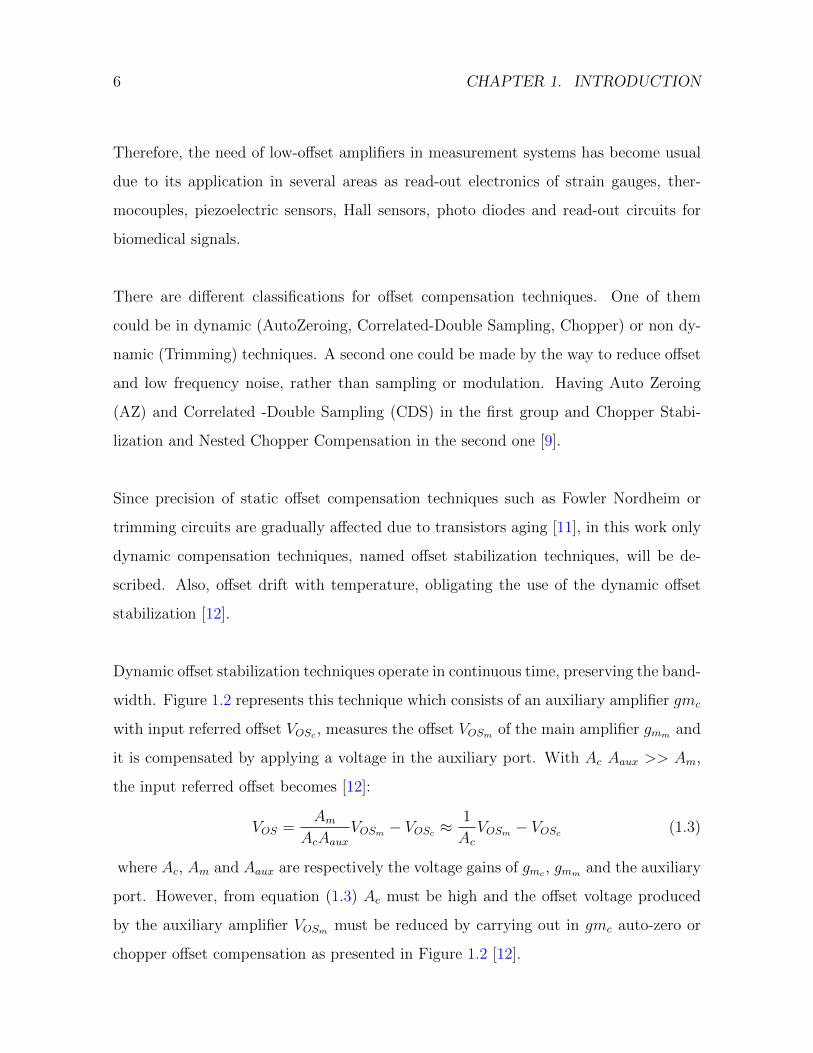
Dynamic offset stabilization techniques operate in continuous time, preserving the band-
width. Figure 1.2 represents this technique which consists of an auxiliary amplifier gmc
with input referred offset VOSc , measures the offset VOSm of the main amplifier gmm and
it is compensated by applying a voltage in the auxiliary port. With Ac Aaux >> Am,
the input referred offset becomes [12]:
VOS =Am
AcAauxVOSm − VOSc ≈
1
AcVOSm − VOSc (1.3)
where Ac, Am and Aaux are respectively the voltage gains of gmc , gmm and the auxiliary
port. However, from equation (1.3) Ac must be high and the offset voltage produced
by the auxiliary amplifier VOSm must be reduced by carrying out in gmc auto-zero or
chopper offset compensation as presented in Figure 1.2 [12].
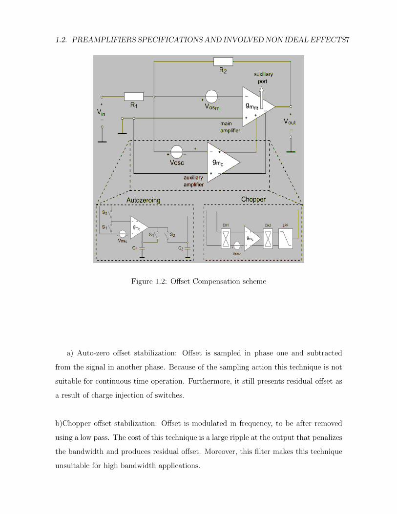
1.2. PREAMPLIFIERS SPECIFICATIONS AND INVOLVED NON IDEAL EFFECTS7
Figure 1.2: Offset Compensation scheme
a) Auto-zero offset stabilization: Offset is sampled in phase one and subtracted
from the signal in another phase. Because of the sampling action this technique is not
suitable for continuous time operation. Furthermore, it still presents residual offset as
a result of charge injection of switches.
b)Chopper offset stabilization: Offset is modulated in frequency, to be after removed
using a low pass. The cost of this technique is a large ripple at the output that penalizes
the bandwidth and produces residual offset. Moreover, this filter makes this technique
unsuitable for high bandwidth applications.

8 CHAPTER 1. INTRODUCTION
To overcome these disadvantages, in this thesis an offset stabilization based on con-
tinuous time DC feedback, quasi-infinite resistors and Quasi Floating Gate transistors
is proposed. Such technique avoids the need of a high gain compensation loop, modu-
lated signals and offset compensation, circumventing charge injection, chopper ripple,
noise folding and bandwidth degradation.
1.3. STATE-OF-THE-ART 9
1.3 State-of-the-Art
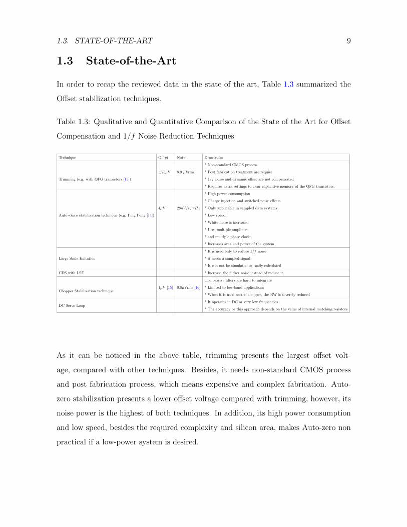
In order to recap the reviewed data in the state of the art, Table 1.3 summarized the
Offset stabilization techniques.
Table 1.3: Qualitative and Quantitative Comparison of the State of the Art for Offset
Compensation and 1/f Noise Reduction Techniques
Technique Offset Noise Drawbacks
Trimming (e.g. with QFG transistors [13])
* Non-standard CMOS process
±25µV 8.9 µVrms * Post fabrication treatment are require
* 1/f noise and dynamic offset are not compensated
* Requires extra settings to clear capacitive memory of the QFG transistors.
Auto−Zero stabilization technique (e.g. Ping Pong [14])
* High power consumption
* Charge injection and switched noise effects
4µV 28nV/sqrtHz * Only applicable in sampled data systems
* Low speed
* White noise is increased
* Uses multiple amplifiers
* and multiple phase clocks
* Increases area and power of the system
Large Scale Exitation
* It is used only to reduce 1/f noise
* it needs a sampled signal
* It can not be simulated or easily calculated
CDS with LSE * Increase the flicker noise instead of reduce it
Chopper Stabilization technique
The passive filters are hard to integrate
1µV [15] 0.8µVrms [16] * Limited to low-band applications
* When it is used nested chopper, the BW is severely reduced
DC Servo Loop* It operates in DC or very low frequencies
* The accuracy or this approach depends on the value of internal matching resistors
As it can be noticed in the above table, trimming presents the largest offset volt-
age, compared with other techniques. Besides, it needs non-standard CMOS process
and post fabrication process, which means expensive and complex fabrication. Auto-
zero stabilization presents a lower offset voltage compared with trimming, however, its
noise power is the highest of both techniques. In addition, its high power consumption
and low speed, besides the required complexity and silicon area, makes Auto-zero non
practical if a low-power system is desired.
10 CHAPTER 1. INTRODUCTION
Chopper presents the lowest noise power in table 1.3, but it requires passive filters
which can not be easily integrated. Besides, this technique has a limited operation
band frequency and when undergo through nested chopper, badwidth may be reduced.
Similarly, DC Servo Loop operation is confined to DC or very low frequencies, and one
of the drawbacks consists in the need of well matched resistors.
In the state of the art for biopotentials readout circuits, topologies that do not use
chopper modulation suffer from 1/f noise while their CMRR is usually limited by com-
ponents mismatch. An alternative is the use of chopper stabilized capacitive-coupled
amplifiers which modulate the input signal before applying it to their input capacitors
and so attenuate 1/f noise and increase CMRR. The disadvantage of this technique
is the reduction of the input impedance, which can be solved by relocating the input
chopper to the virtual ground inside the feedback loop. However, this approach limits
the CMRR because of the capacitor mismatch. This disadvantages could be overcome
using a chopper stabilized current amplifier with voltage follower inputs [2], however
the offset rejection capability will be limited.
Next, Tables 1.4, 1.5 and 1.6 present a quantitative and qualitative comparison re-
spectively of the biomedical FE acquisition systems reviewed.

1.3. STATE-OF-THE-ART 11
Table 1.4: State of the Art Quantitative Comparison for Biomedical Acquisition Sys-
temsParameter [17] [18] [19] [20] [21]
Technology 0.5µm 0.5µm 0.5µm 0.5µm 0.5µm
Supply (V) 3.3 ±1.5 3.3 3 3.3
Current (A) 12.8µ - - 20µ 16.5µ
Voltage Gain (dB) 60 67.7/77.1 ** 48-57/75-79 ** 52/58/63/68 ** 48
HP f−3dB(Hz) 30-1K * 0.1-1K * 0.7-1.95 * 0.3-0.34 * 250
LP f−3dB(Hz) 700-10K * 300-5.4K * * 14-15.8 * *
Input Referred Noise (µVrms) 5.1 3.9(10Hz-10KHz) 5.8 2.4
NEF 4.1 - - - 4.2
THD (%) - 1(40% full swing) - 0.45-0.52 -
CMRR (dB) - 139 - >120 >107@5KHz
PSRR +/- (dB) - 65/- - >80/>78 -
Power (W) - - 13.7 µ per channel 60µ 54.4µ
Area (mm2) - - 0.12 per channel 1.95 -
*tunable frequency, ** tunable gain
Table 1.5: State of the Art Quantitative Comparison for Biomedical Acquisition Sys-
temsParameter [22] [2] [23] [24] [25] [26] [27]
Technology 90nm 0.18µm 0.18µm 0.18µm 0.35µm 0.35µm 0.35µm
Supply (V) 3 1.8 1.8 1 1 0.8-1.5 1
Current (A) 35.5µ 11µ - 21µ 1.26µ 330n 33n/337n
Voltage Gain (dB) 54/68 ** 40 20/60 ** - 45.7/49.3/53.7/605 ** 40.2 45.6/49/53.5/60 **
HP f−3dB(Hz) 0.4* - - - 0.23-217* 3m 4.5m-3.6 *
LP f−3dB(Hz) * - - - 7.8K 245 31-202
Input Referred Noise (µVrms) 51.4nV/√Hz 0.8(0.5Hz-100Hz) 2.2(1Hz-1KHz) 1.9 4.43(1Hz-12KHz) 2.7 2.5(0.05Hz-460Hz)
NEF 8.5 12.3 - - 2.16 2.8 3.26
THD (%) 0.77 - - - 0.53(full swing) 0.05 0.6
CMRR (dB) 140 82 - 100 58 61/64 >71.2(up to 300Hz)
PSRR (dB) - 40 67 - 40 62/63 >84(up to 300Hz)
Power (W) 106.5µ - 323.5µ 36µ 3.77µ per channel 3.4µ 445n-895n
Area (mm2) - 6.48 11.23 9 - 1 1
*tunable frequency, **tunable gain
12 CHAPTER 1. INTRODUCTION
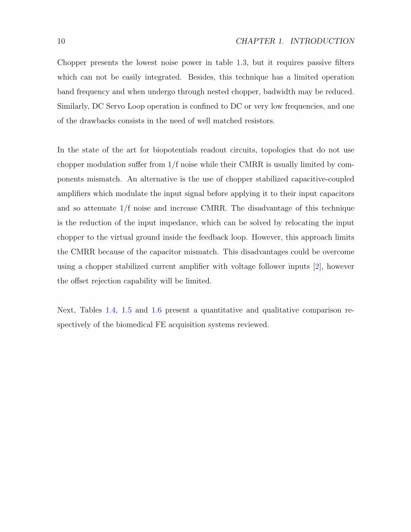
Table 1.6: Qualitative and comparative description of the Biomedical Acquisition Sys-
tems in the State of the Art
Scope Features Technique
Active Electrode System for Monitoring [2]
*Front End System *CMRR: Back End CMFB
*Preamplifier with BPF *Offset: Digitally assisted Offset Trimming
*8 Channels System *Noise: Chopper
*Capacitive Feedback *Other: Input impedance boosting
Implantable Neural Recording [25]
*16 Channels FE with PGA *CMRR: -
*tunable HP f−3db of BFP and *Offset: -
*4 Gain settings *Noise: -
*10 bit-SAR ADC dual capacitive array *Other: Bootstrapped technique
Wireless Neural Recording System [17]
Rectifier, Voltage regulator, clock and command recovery *CMRR:
100-Electrode System, 10-bit charge redistribution ADC *Offset:electrode ac coupled with the amplifier
10x10 array of neural amp and spike detectors *Noise: use large PMOS devices
433-MHz FSK data transmitter
Wireless Neural Recording System [18]
32-ch implantable with adjustable resolution BPF CMRR:
Based on time division multiplexing of PWM signals Offset:
The FE consists of an array of 2 tage capacitvely coupled LNAs Noise:
Low cutt-off tunable via pseudo resistors
Neural Recording Amplifier [19]
*Preamplifier with BPF and simple noninverting amplifier *CMRR:
*Two Programmable Gain and *Offset:
*Two Programmable BW with 2 Bits each one *Noise:
*PMOS resistance and capacitive feedback
Readout FE for Portable Biopotential [20]
*FE for Portable Biopotentials *CMRR: Chopper
*ACCIA, Chopping Spike Filter and VGA stages *Offset: AC Coupling
*Digitally controlable Variable Gain and BW *Noise: Chopper
FE ASIC for EEG [23]
*8 Channels Mixed-Signal FE ASIC for EEG *CMRR:
*Preamplifier with variable gain *Offset: Compensate Digitally by 2 current mode DACs
*RC LPF and Switch Capacitor LPF with 2 selectable bands *Noise: Low noise non inverting Op Amp with resistive feedback
*12 Bit SAR ADC *
Adaptive Interface for Portable Biomedical [24]
*FE IA with BPF, PGA and SAR ADC *CMRR:
*Gain and BW digitally controllable *Offset: ADC
*10 bits adaptable SAR ADC *Noise: Chopper
*Adaptive Control
Biomedical Signal Acquisition IC [26]
*Low noise IA with DC rejection *CMRR
*capacitor array based 11 bit SAR ADC *Offset
*DC rejection using pseudo resistors *Noise: Current steering logic gates to reduce switching noise.
*Start up circuit
Programmable Biomedical Sensor Interface [27]
*Tunable BW - FEA *CMRR
*PGA with 4 levels voltage gain *Offset: Balance Tunable Pseudo-resistor
*12 Bit SAR ADC *Noise:Large gate area input transistors
*Relaxation Oscillator *Other: flip-over capacitor in feedback loop
Neural Recording Amplifier [21]
*Assymetrical Diferential Diference Amplifier (DDA) *CMRR: Assymetrical DDA
*A local feedback at the amplifier output *Offset:Local feedback at the amplifiers output
*DDA realized with 2 OTAs with different transconductance *Noise:
Biopotential Signal Readout FE [22]
*Front stage IA *CMRR:
*Gain and BW adjustable via internal resistor *Offset:Chopper
*AC coupler and Chopper notch filter Noise: Thick and thin oxide of the transistors
*Noise: aware transistor (thick and thin oxide)

1.3. STATE-OF-THE-ART 13
Note that according to the three latter tables, five of twelve state-of-art biomedical
acquisituion systems are designed and fabricated using a 0.5µm CMOS technology, and
four of them count on tunable frequency and/or tunable gain. A similar case is pre-
sented in Table 1.5, where it can be noticed that four of the seven works listed, count
on the tunablilty feature. Such list shows sub-micrometric front-end systems and [26]
with a technology of 0.18µm presents the best power noise value. However, the same
table lists the largest power consumption, presented in [23].
In table 1.6 a state of art qualitative description of the biomedical acquisition sys-
tem is presented. Note that more than half of the listed works, lack CMRR reduction
techniques and one third of the works implement some offset compensation technique.
On the other hand, all the works but two in the list, count on certain noise reduction
approach.
Table 1.7 represents a quantitative description of biomedical acquisition systems re-
viewed, emphasizing on their CMRR, noise and offset performance. Common Mode
Rejection Ratio ranges from 58dB to 140dB, while the offset levels are in between
20mV to 50mV. Finally, noise range in table 1.7 goes from 0.8µVrms up to 5.8µVrms.
The Table 1.7 represents a quantitative description of biomedical acquisition systems
reviewed, emphasizing on their CMRR, noise and offset performance.
As it can be observed, the smallest level of noise is presented in [2]. Respect to offset
performance, the best achieved value by 4 references is of 100mV; The best CMRR is
achieved with a 90nm process technology, up to 140dB.
Equations (1.4) and (1.5) describe the Noise Efficiency Factor and a Figure of Merit
commonly used in the blocks of a front-end amplifiers and band pass filters respectively.

14 CHAPTER 1. INTRODUCTION
Table 1.7: Quantitative and comparative description of the Biomedical Acquisition
Systems in the State of the Art
Reference CMRR Offset Noise
[2] 82db @50Hz 20mV 0.8µVrms(0.5-100Hz)
[25] 58db - 4.43µVrms(1Hz-12KHz)
[17] - - 5.1µVrms
[18] 139 - 3.9µVrms(10Hz-10KHz)
[19] - - 5.8µVrms
[20] 120dB ±50mV 57nV/√Hz
[23] - - 2.2µV(1Hz-1KHz)
[24] 100dB 100mV 1.9µVrms(0.1Hz-200Hz)
[26] 61-64dB 100mV 2.7µVrms(0.05Hz-245Hz)
[27] 71.2dB up to 300Hz 2.5µVrms(0.05Hz-460Hz)
[21] >107dB 2.4µvrms
[22] 140 dB up to 1KHz ±50mV 51.4nv/√Hz
NEF = V rms, in
√2 ∗ ITotal
π ∗ UT ∗ 4kT ∗BW(1.4)
FoM =P ∗ VDD
η ∗ fc ∗DR(1.5)

1.3. STATE-OF-THE-ART 15
Table 1.8: State of the Art of Notch Filters
Reference [28] [29] [30] [22]
Technology 0.18µm 0.6µm 90nm 90nm
Power Supply Voltage [V] 1.8 - 3 3
Center Rejection Freq [Hz] 50 50 50/60 50
Center attenuation [dB] 55.4 58.5 25/41 41
Q 1.17 - 0.1/0.5 -
Input Refered Noise [µV/√Hz] 4.12@(1KHz) - - -
PSRR [dB] 65 - - -
Dynamic Range [dB] 78 - - -
Upper−3dBFreq [Hz] 71.6 - - -
Lower−3dBFreq [Hz] 29 - - -
Power Consumption [µW] 25.2 - 75 -
Die area [mm2] 0.06 - - -
Tables 1.8 and 1.9, summarize the quantitative description of notch and band pass fil-
ters respectively, reviewed in the state of the art. Reference [30] summarized in Table
1.8 presents two modes of selectivity in center rejection frequency, center attenuation
and quality factor. Reference [28] is the only one that exhibits an input referred noise
measurement at 1KHz of 4.12µV/√Hz. Most of works presented are designed to re-
ject a 50Hz frequency. In table 1.9 references [31], [32] and [34] present selectivity in
bandwidth, a reduced power consumption down to 14.4nW and up to 1.2µW. All these
filters are designed with a fourth order topology.

16 CHAPTER 1. INTRODUCTION
Table 1.9: State of the Art of Band Pass Filters
Reference [31] [32] [33] [34]
Technology 0.35µm 1.5µm BiCMOS 0.35µm 0.18µm
Power Supply Voltage [V] 1 2.8 2.2 1
Noise [µVrms] - 776/796 19µV/√Hz 50
THD [%] - - - 1
Order 4 4 4 4
Center Freq [Hz] - - 54M-74M 732
DR [dB] - 67.5/65 - 55
Power Consumption [W ] 1.2µ 230n/6.36µ - 14.4n
FoM - - - 0.89×10⁻¹³
Area [mm2] - - - 0.132
BW Hz 40-90 100-200/5K-10K - 523-1024
Sampling Freq [KHz] 1 - - -
In Band Gain [dB] 44.5 - - -
Q - - 5-110 -

1.4. GOALS AND DESCRIPTION OF THIS WORK 17
1.4 Goals and Description of this work
−
+−
+−
+
OUTSKIN
ELECTRODELNA
BPF NOTCH
PGA ADC
−
+−
+
Vp
Vn
CMRREnhancement
Circuit
auxport1
auxport2V outnamp
V outpamp
OFFSET
COMPENSATION
FE - Amplifier
Figure 1.3: Block Diagram for an EEG acquisition system
The design and simulation of a Biopotential Acquisition System is presented in this
work. Specifically, the design of both, low noise dynamic offset compensated preampli-
fier and the proper band limiting filter are described.
The amplifier design will avoid some of the auto-zero stabilization disadvantages (e.g.
charge injection, requirement of a multi-phase local oscillator, increase of low frequency
noise) and those from chopper stabilization (local oscillator, charge injection, output
signal ripple), preserving flicker noise levels low enough to sense signals within ECG,
EEG and EMG band frequencies, listed in Table 1.1.
Next questions must be answered with aim on making advances on the state-of-the-
art of low noise preamplifiers:
• In order to avoid problems related to switches in offset stabilization techniques:
is it possible to perform DC Feedback offset compensation, not affecting the input
18 CHAPTER 1. INTRODUCTION
equivalent noise and satisfying ECG, EEG and EMG requirements?.
• According to equations 1.1 and 1.2, there is a codependency between CMRR and
Offset, then: is it possible to incorporate a CMRR enhancement block with the
amplifier design, in order to improve the most important figures of merit of the
amplifier, such as input equivalent offset, PSRR, THD and power consumption?.
• In order to reduce silicon area and enable the use of on-chip capacitors, is it
possible to incorporate HVTR (high resistive elements) with the design of the
low-pass filter including in the offset compensation scheme?, does this affect any
figure of merit?.
• A low noise folded cascode amplifier is designed, starting from design equations in
Chapter 3. A folded cascode amplfier (FCC) topology is selected since it counts on
a good tradeoff between gain, bandwidth and hardware complexity. Specifications
based on state-of-art of tables 1.4 and 1.5 are listed next:
Montecarlo analyses based on Pelgrom’s missmatch model [35] are performed along
with the simulations.
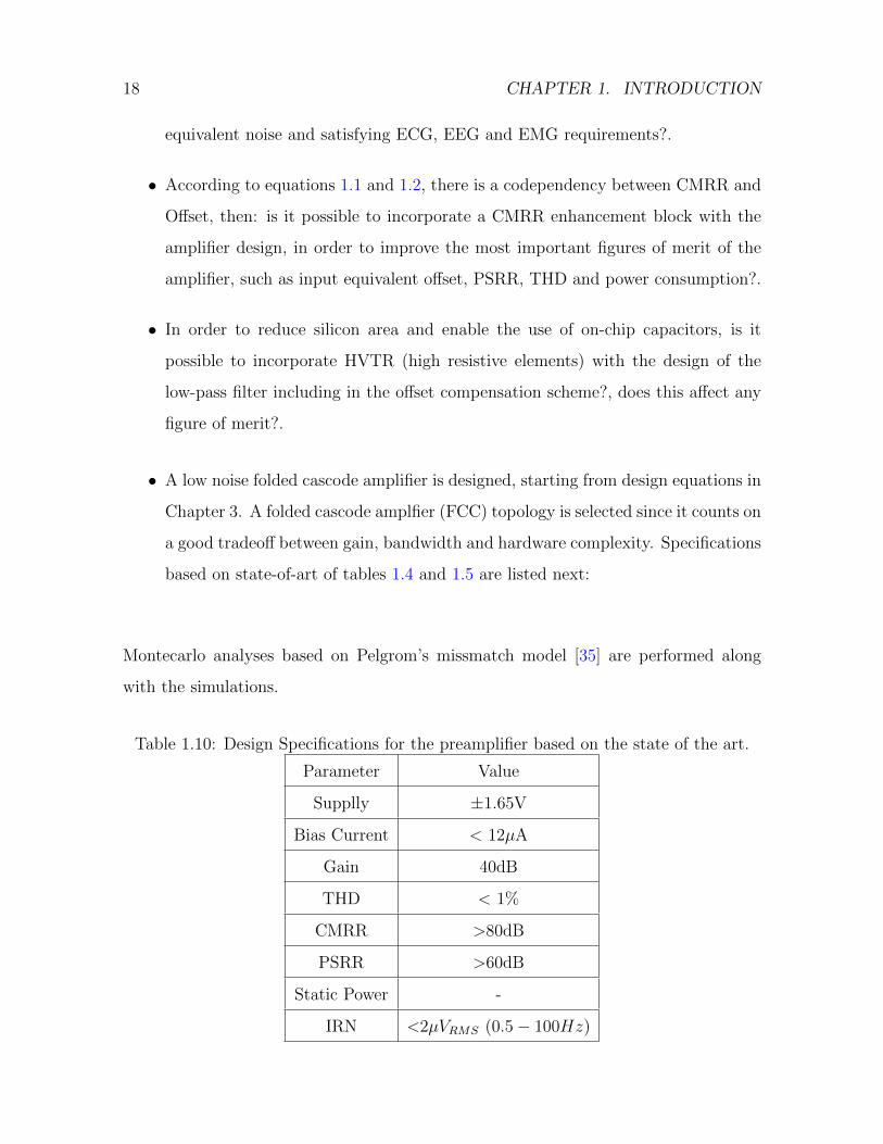
Table 1.10: Design Specifications for the preamplifier based on the state of the art.
Parameter Value
Supplly ±1.65V
Bias Current < 12µA
Gain 40dB
THD < 1%
CMRR >80dB
PSRR >60dB
Static Power -
IRN <2µVRMS (0.5− 100Hz)
1.4. GOALS AND DESCRIPTION OF THIS WORK 19
• A CMRR enhancement block is added to the FCC topology, comparing simula-
tions performance of the FCC amplifier with and without such block.
• An Offset Compensation DC Feedback circuit is attached to the FCC amplifier.
Performance of the original FCC amplifier and the one with offset compensation
are compared by simulation.
• Both, Offset and CMRR compensation blocks are attached to the FCC amplifier
and simulation results are compared
• Besides of improvements of the figures of merit, the reuse of circuit blocks is
attempted. It is particularly desirable exploit the capactive feedback and the
input QFG transistors to perform the low-frequency filtering function of the offset
compensation.
Based on state-of-the-art tables 1.8 and 1.9, and specs presented in Table 1.1, next
research questions are presented, regarding to the band limiting filter:
• Is the filter electrically tunable in order to fulfill the ECG, EMG and EEG fre-
quency band requirements?.
• Could the filter be designed including HVTR to achieve all capacitors to be on-
chip?.
• Are both filters, notch and bandpass tunable?.
• Is it possible to stablish a very low power consumption of the filter to take as
much power as possible in the input stage (preamplifier)?.
Next methodology is presented to design the filters:
• A band-pass topology is chosen, which is made up by a high-pass first stage
and a low-pass second stage, in order to have the cut-off frequencies tunability
independently one of each other.
20 CHAPTER 1. INTRODUCTION
• HVTR elements are used with the aim of achieve cut frequency selectivity. Fea-
tures of HVTR allow modification of the system RC constant. This is accom-
plished varying the resistivity of such elements, by means of different bias volt-
ages.
In order to reduce some undesirable effects in the acquired signal due to external cable
motion or mains, a 50/60 Hz stop band filter has been proposed with the next design
methodology:
• A twin tee topology with reduction of silicon area and power consumption has
been chosen, hence the Q of this filter is directly dependent on its resistances
value.
• The large time constants has been obtained with small on chip capacitors an
HVTR avoiding the demand of external pads and representing area reductions
respectively.
• The use of the HVTR elements working in subthreshold region let us obtain a
wide range of tunability ot the resistance, achieving a large tunability in band.
• The stop frequency tunability may be selectable through an HVTR as well as
the BW may be selectable by another HVTR independently. The resistance of
these HVTRs is selectable trough their voltage control which is tunable with an
external bias source with a step of selectivity of 10mV.
• So, with a tunable fc and BW the quality factor (Q) of the notch filter may be
modified. The design specifications of Q has been set at 10, and the RC elements
has been sizing to meet with this specification.
The structure of this thesis is organized as follows: Chapter 2 includes the theoretical
framework of this work, which consist of the principles of design and techniques. In
chapter 3, the proposed design techniques for each block are presented. The preampli-
fier consist of a low noise amplifier with high gain, and low power consumption based
on a Folded Cascode Topology (FCC).
1.4. GOALS AND DESCRIPTION OF THIS WORK 21
A CMRR enhancement technique presented in [36] is used to achive a high CMRR with
the improvement of monte carlo simulations do to mismatch between inverter blocks.
An offset compensation scheme performed by an inverter amplifier whose output signal
is reinserted in the system throughout the reference voltage node in a quai floating
gate (QFG) transistor. The tunable band pass filter is implemented with a three order
scheme conformed by OTA amplifiers and a two stage high pass and low pass config-
urations made with fixed capacitors and high value tunable resistors. The notch filter
is implemented with a twin tee topology, achieving the tunability of this block with
the use of high voltage tunable resistors as well as in the previous block. In chapter 4,
simulation results for each component of the FE system are presented, with summary
tables that presents the performance of the amplifiers used in each block and the main
characteristics of each design. The system was design in 0.5um AMI process. Finally,
conclusions and future work of this thesis are discussed in chapter 5.

22 CHAPTER 1. INTRODUCTION

Chapter 2
Theoretical Framework
2.1 Thermal Noise
Thermal noise is generated only in dissipative systems. Therefore, it is associated with
all resistors and lightly doped semiconductor layers [39].
a) Resistor Thermal Noise.
Thermal Noise in resistors is caused by brownian motion of electrons in a conduc-
tor, and introduces fluctuations in the measured levels of voltage or current across the
resistor. The DC component of the fluctuation is zero [39]. The Nyquist’s Theorem
states that for linear resistances in thermal equilibrium at temperature T, the current
or voltage fluctuations are quite independent of the conduction mechanisms, type of
material, shape and geometry of the resistor. The generated noise depends exclusively
upon the value of the resistance and its temperature T (given in kelvins) [39]. Hence,
the spectrum of thermal noise is proportional to the absolute temperature. The thermal
noise of a resistor R can be modelled by a series voltage source (Thevenin equivalent)
or parallel current source (Norton equivalent) as shown in Figure 2.1.
23

24 CHAPTER 2. THEORETICAL FRAMEWORK
R
+−
V 2n
Noiseless Resistor
Sv(f)
f
4kTR
Figure 2.1: Thermal noise of a resistor
Assuming ∆f = 1Hz the noise spectral density and the noise voltage and current
spectral densities are represented by:
Sv(f) = 4kTR∆f, [V 2/Hz] (2.1)
S(Vn) =V 2n
∆f= 4kTR, [V 2/Hz] (2.2)
S(In) =i2n
∆f=
4kT
R= 4kTG, [A2/Hz] (2.3)
where k = 1.38x10⁻²³[J/K] is the Boltzmann constant. Note that Sv(f) is expressed in
V 2/Hz and can be written as V 2n [5].
b) MOS Thermal Noise.
The most significant thermal noise source in a MOS transistor is the noise generated in
the channel. For long-channel MOS devices operating in saturation region, the channel
noise can be modelled by the circuit presented in figure 2.2 with a spectral density given
by (2.4).
I2n = 4kTγgm
Figure 2.2: Thermal noise of a MOS transistor

2.2. FLICKER NOISE 25
I2n =
id2
∆f= 4kTγgds (2.4)
with VDS = 0, gds is the transconductance of the transistor in saturation region. The
correction factor γ is called the excess-noise factor, and it has a value close to unity for
the linear region and 2/3 for a long channel-saturated transistor in strong inversion [40].
In weak inversion, the spectral density becomes:
I2d
∆f= 4kT
gs + gd2
(2.5)
For a saturated transistor in weak inversion (gs gd) is considered.
2.2 Flicker Noise
All active devices and some passive devices, such carbon resistors, a band of noise at
low frequencies, in addition to thermal noise, which is called flicker excess noise (1/f
noise) [40]. The 1/f noise has many unique properties, such is the limitless increment of
the noise spectral density with the frequency decrement. The main cause of 1/f noise
in semiconductor devices is referable to properties of the surface energy states and the
density of surface states. Improved surface treatment in manufacturing has decreased
1/f noise, but even the interface between silicon surfaces and grown oxide passivation
are noise sources [7].
Unlike thermal noise, the average power of flicker noise cannot be easily predicted.
Hence, there is no universal mechanism responsible for 1/f noise. A procedure to deter-
mine 1/f noise parameters appart of noise measurements is not known. However some
equations for a first hand calculations are presented next.
a) Flicker Noise in Integrated Resitors.
The 1/f noise voltage developed in integrated resistors has the general form given
by equation 2.6.

26 CHAPTER 2. THEORETICAL FRAMEWORK
V 2n = KR
R
ARV 2DC
δf
f(2.6)
where VDC is the DC voltage across the resistor, R is the sheet resistance, AR is the
area of the resistor, and KR is a technological constant. For a diffused or ion-omplanted
resistor, KR∼= 5x10⁻²⁴[S2cm2], while for thick-film resistors, it is aproximated 10 times
greater [39].
b) Flicker Noise in CMOS devices.
The effect that dominates flicker noise in MOSFETs is when electron tunnel from traps
in the oxide to the gate and the conducting channel, and vice versa. It is modelled as a
voltage source in series with its gate (see Figure 2.3) and its spectral density is roughly
given by:
20logV 2n
logf
Figure 2.3: Flicker noise of a CMOS Transistor
V 2g
∆f=
KF
CoxWL
1
f(2.7)
where KF is a process-dependent constant on the order of 10−25[V 2F ].
The only way to achieve a significantly flicker noise reduction is to lower the surface-state
density in the vicinity of the Fermi level. Moreover, 1/f noise increases with decreasing
temperature. For MOS transistors operating in strong inversion, flicker noise does not
2.3. NOISE IN CMOS AMPLIFIERS 27
depend on the gate bias, because the surface potential varies very slowly with gate
charge. In this case the only way to significantly lower the noise level is to modify the
device geometry [39].
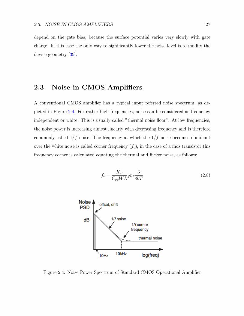
2.3 Noise in CMOS Amplifiers
A conventional CMOS amplifier has a typical input referred noise spectrum, as de-
picted in Figure 2.4. For rather high frequencies, noise can be considered as frequency
independent or white. This is usually called ”thermal noise floor”. At low frequencies,
the noise power is increasing almost linearly with decreasing frequency and is therefore
commonly called 1/f noise. The frequency at which the 1/f noise becomes dominant
over the white noise is called corner frequency (fc), in the case of a mos transistor this
frequency corner is calculated equating the thermal and flicker noise, as follows:
fc =KF
CoxWLgm
3
8kT(2.8)
Figure 2.4: Noise Power Spectrum of Standard CMOS Operational Amplifier
28 CHAPTER 2. THEORETICAL FRAMEWORK
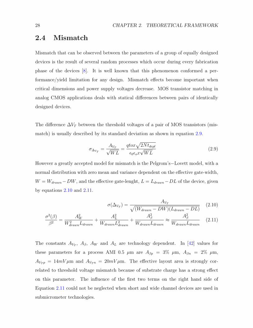
2.4 Mismatch
Mismatch that can be observed between the parameters of a group of equally designed
devices is the result of several random processes which occur during every fabrication
phase of the devices [8]. It is well known that this phenomenon conformed a per-
formance/yield limitation for any design. Mismatch effects become important when
critical dimensions and power supply voltages decrease. MOS transistor matching in
analog CMOS applications deals with statical differences between pairs of identically
designed devices.
The difference ∆VT between the threshold voltages of a pair of MOS transistors (mis-
match) is usually described by its standard deviation as shown in equation 2.9.
σ∆VT=
AVT√WL
=qtox
√2Ntdepl
ε0εox√WL
(2.9)
However a greatly accepted model for mismatch is the Pelgrom’s−Lovett model, with a
normal distribution with zero mean and variance dependent on the effective gate-width,
W = Wdrawn−DW , and the effective gate-lenght, L = Ldrawn−DL of the device, given
by equations 2.10 and 2.11.
σ(∆VT ) =AVT√
(Wdrawn −DW )(Ldrawn −DL)(2.10)
σ2(β)
β2=
A2W
W 2drawnLdrawn
+A2L
WdrawnL2drawn
+A2β
WdrawnLdrawn≈
A2β
WdrawnLdrawn(2.11)
The constants AVT , Aβ, AW and AL are technology dependent. In [42] values for
these parameters for a process AMI 0.5 µm are Aβp = 3% µm, Aβn = 2% µm,
AVT p = 14mV µm and AVTn = 20mV µm. The effective layout area is strongly cor-
related to threshold voltage mismatch because of substrate charge has a strong effect
on this parameter. The influence of the first two terms on the right hand side of
Equation 2.11 could not be neglected when short and wide channel devices are used in
submicrometer technologies.
2.4. MISMATCH 29
Accordingly with Pelgrom in [35], the most important contribution to the propor-
tionally constant AVT is the uncertainty in the number of active doping atoms in the
depletion layer (N). The statistical variations in N = (Na+Nd) determines the match-
ing while control in the net value (Na−Nd) determines the threshold voltage VT .
The Monte Carlo analysis allows the evaluation of the variation of desired circuit per-
formance, and subsequently, yield predictions.
In order to implement analog circuits, matching must be characterized by two indepen-
dent statistical values: threshold mismatch ∆V T which may have in practice a mean
standard deviation ranging from 1 to 20 mV, and ∆β/β mismatch which is usually in
the range of 0.5 to 5 percent. From [47] is demonstrated that when two transistors have
the same gate voltage, as in a current mirror structure, the mismatch of their drain cur-
rents is maximum in weak inversion with (if << 1, and thus with the maximum gm/ID
), whereas the minimum current mismatch, is obtained with the transistors operating
deep in strong inversion. This can be observed in equation 2.12.
∆IDID
=∆β
β− gmID
∆VT (2.12)
On the other hand, for a differential pair, operation of the transistors in weak in-
version results in the minimum mismatch between the gate voltages and it is given by
equation 2.13.
∆VG = ∆VT0 −IDgm
∆β
β(2.13)
As presented before, mismatch of active and passive devices represents a major limita-
tion to the accuracy of analog circuits. Single-stage cascoded OTA’s should be preferred
to multistage amplifiers. Notice that in strong inversion where gm/ID is reduced, mis-
match increase.
30 CHAPTER 2. THEORETICAL FRAMEWORK
2.4.1 The Speed, Accuracy and Power Tradeoff
As shown earlier in this text, mismatch can be reduced by increasing the transistor’s
dimensions, but the speed-accuracy-power tradeoff is seriously affected. As presented
in [42], for most of current and voltage processing circuits, this tradeoff only depends
of technological and mismatch parameters as in Equation 2.14.
Speed ∗ Accuracy2
Power∝ 1
CoxA2VT
(2.14)
2.5 Dynamic Range and Distortion
2.5.1 Distortion
In analog circuits, precision requirements allow small non linearities, which make possi-
ble to approximate the input/output characteristic by a Taylor expansion in the range
of interest:
y(t) = α1x(t) + α2x2(t) + α3x
3(t) + ... (2.15)
For small x, y(t) ≈ α1x, indicating that α1 is the small-signal gain in the vicinity of x
≈ 0.
The nonlinearity of a circuit can be also characterized by applying a sinusoid at the input
and measuring the harmonic content of the output. In that fashion, if x(t) = Acosωt,
then:
y(t) = α1Acosωt+α2A
2
2[1 + cos(2ωt)] +
α3A3
4[3cosωt+ cos(3ωt)]... (2.16)
It can be observed that higher order terms yield higher harmonics. In particular, even
and odd order terms result in even and odd harmonics, respectively. Note that the
magnitude of the nth harmonic grows roughly in proportion to the nth power of the
input amplitude. This effect called ”harmonic distortion” (HD) is usually quantufied
by summing the power or all of the harmonics (except that of the fundamental) and
normalizing the result to the power of the fundamental. Such a metric is called the
2.6. QUASI FLOATING GATE (QFG) TECHNIQUE 31
”Total Harmonic Distortion” (THD). As an example for a third order nonlinearity, from
2.17 [5].
THD =(α2A
2/2)2 + (α3A3/4)2
(α1A+ 3α3A3/4)2(2.17)
Harmonic Distortion is undesirable in most signal processing applications. An impor-
tant property that must be remarked is that differential mode circuits which are driven
by a differential signal produces no even harmonics, unlike exhibit an odd-symmetric
input/output characteristic. For the Taylor expansion of 2.15 to be an odd function,
all of the even order terms, α2j must be zero, as presented in equation 2.18 [5].
y(t) = α1x(t) + α3x3(t) + α5x
5(t) + ... (2.18)
There are different linearization techniques in the literature, as presented in [5], some of
them are: switched capacitor (SC) topologies, source degeneration method, operating
transistors in triode region, etc.
2.5.2 Dynamic Range
Dynamic Range (DR) is defined as the ratio between the maximum input signal,
Vrms,max driven by electronic devices to ensure a Total Harmonic Distortion (THD)
lower than a specified value to the device’s input referred noise [4], Vin,noise, i.e.
DR =Vrms,maxVnoise,in
(2.19)
2.6 Quasi Floating Gate (QFG) Technique
A quasi floating gate MOS (QFGMOS), is a FGMOS transistor whose gate is tied to a
very large value resistor that weakly connects it to a voltage to establish the operating
point. Figure 2.5 represents a 4 input n-channel QFG [43].
For a generic N-input QFG, the voltage at the gate is given by equation 2.20.

32 CHAPTER 2. THEORETICAL FRAMEWORK
Figure 2.5: Quasi Floating Gate MOS Equivalent Circuit
VFG =sRleak
1 + sRleakC ′T(Σi = 1NCi · Vi + CGS · VS) + CGD · VD) (2.20)
where all the voltages have been referred to the bulk and C ′T is the total capacitance
seen by the gate of the Quasi-FGMOS. It follows from 2.20 that the inputs are high-pass
filtered with a cutoff frequency which is inversely proportional to Rleak. Hence, as long
as Rleak is kept high enough, the gate can be effectively floating for very low frequency
values so that the AC operation is unaffected [43].
The total capacitance seen by the QFG is given by eq. 2.21.
CT = CGD + CGS + CGB +N∑i=1
Ci (2.21)
Since Rleak is implemented using an active device, its parasitic capacitances should
be added to equation 2.21. It is important to remark two drawbacks of the FGMOS
compared with MOS transistor: the reduction of the input transconductance and the
output resistance, as well as the high input impedance.
2.7 High-Value Tunable Resistor
Since it is unpractical to realize high value passive resistors due to area implications, the
need of integrated high-value resistors or Quasi Infinite Resistors (QIRs) is important.
They are used in many applications like biasing purposes or for implementing very low
frequency filters. In addition to high resistance, the tuning capability of the resistor
value of the QIR is an important design issue [49].

2.7. HIGH-VALUE TUNABLE RESISTOR 33
Different topologies can be found in recent works [11], [49], [50], four of them will be
presented along their principal advantages and disadvantages.
Figure 2.6: Basic Structures of Floating QIRs (a) A Cross section view of a PMOS
transistor and its associated PN junctions. (b) QIR Electrical model of Figure 2.6(a).
(c)Electrical Model of a Low swing QIR. (d) Electrical Model of a moderate swing QIR.
(e)Electrical Model of a Large-Swing QIR.
The basic structure of Floating QIRs is presented in Figure 2.6(a), while its electrical
realizattion can be appreciated on Figure 2.6(b) which constitute the first one of the
four that will be described.
This first of them is implemented with the reverse biased drain-well junction of a PMOS
transistor operating in cutoff region with VC = VDD. One of the problems of this topol-
ogy is the limited swing which should be less than 0.3V in order to prevent the forward
bias of the junction which generate a resistance reduction. Another problem is the
associated with the reverse biased junction formed by the nwell to p-substrate junction
which generate a Rleak which is connected to a power rail, and its resistance forms a
voltage divider with the floating junction implementing RG, which produces an un-
wanted and not predictable DC voltage droping in RG. It is important to notice that
the PNP parasitic transistor will be activated if the junction that generate RG becomes
forward biased.
34 CHAPTER 2. THEORETICAL FRAMEWORK
The second realization is shown in Figure 2.6(c). It consists of a minimum sized PMOS
transistor (MP2), biased to work in weak inversion region by the voltage Vcp. Ergo,
RG Rleak should be assured in order to have a negligible voltage drop in RG. How-
ever the main disadvantaged of this model is that RG values must be limited below
VTH0 so that it keeps MP2 in week inversion.
The third realization, shown in Figure 2.6(d), employs two minimums sized PMOS
diode connected transistors with the purpose to increase the signal range which will be
now restricted by Vswing > VTH .
To improve the voltage swing of the resistor, Figure 2.6(e) presents a series combi-
nation of minimum size PMOS and NMOS transistors. Their control voltages Vcn and
Vcp hold Mn2 and MP2 in the weak inversion region. That holds the effective resistance
of the series combination very large, typically in the order of Giga − ohms, in spite
of large voltage variations in A and B terminals. For the reason that, under dynamic
conditions, variations in either the positive or negative direction tends to turn on one
transistor meanwhile turn off the other one. Therefore, to avoid the parasitic resistive
divider, to operate in weak inversion forces RG Rleak [42].
2.7.1 Tunable Resistor R2
One of the implementations previously presented to obtain an electronically programmable
linear resistor, R2, is realized using the channel resistance of a MOS transistor (MP1)
biased to operate in triode region. According to [?], a first order approximation of R2
is given by equation 2.22 and its circuit implementation is depicted in Figure 2.7.
R2(Vcq) =1
β(Vcq − VA − |VTp|)(2.22)
where β = µpCOX(W/L), VTP and VA are the transconductance factor, threshold
voltage and source voltage, respectively. Vcq is the temperature independent bias voltage
by means the value of R2 is tuning throughout the gate of MP1 which is biased by the

2.7. HIGH-VALUE TUNABLE RESISTOR 35
Ca Ca
Vcq
A BMp1
Mp2
A B
Vcq
Figure 2.7: Circuit Implementation of Tunable R2
transistor MP3 working as a reverse biased pn junction. The disadvantages of this
configuration are the significant distortion presented in triode mode transistors, the
body effect and the mobility degradation. A solution for this problem is the so called
”common mode” linearization technique illustrated in figure 2.7. The signal component
corresponding to the average of the voltages in terminals A and B is added to the gate
voltage VG through two small capacitors Ca, and the gate voltage becomes as equation
2.23. It is important to note that DC components VA and VB do not affect VG because
of the action of the low-frequency high-pass filter Ca −RDS,Mp3.
VG =(VA + VB)
2+ Vcq (2.23)
The low-frequency high− pass filter conformed by Ca−RDS,MP3 preclude the effect of
the DC components VA and VB in VG [?]
2.7.2 High Value programmable resistor Rg
In this case Rg is conformed by the drain-to-source resistance of the transistor MP2.
The use of three transistors in this model presented in Figure 2.8 has the purpose of
prevent large distortion components because of large signal fluctuations across nodes
A and B. The temperature-independent quiescent voltage Vcf establishes the DC gate
voltage by MP3 and impose subthreshold operation in transistors MP2, allowing a wide-
range of tunability and avoiding the effect of the parasitic resistive divider Rg-Rleak. As
36 CHAPTER 2. THEORETICAL FRAMEWORK
Ca Ca
Vcf
A BMp1 Mp2 Mp3
Mp4
A B
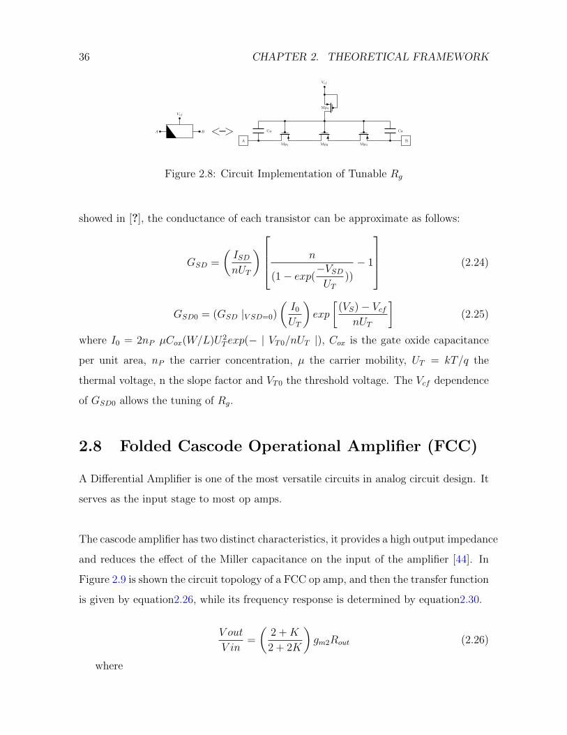
Vcf
Figure 2.8: Circuit Implementation of Tunable Rg
showed in [?], the conductance of each transistor can be approximate as follows:
GSD =
(ISDnUT
) n
(1− exp(−VSDUT
))− 1
(2.24)
GSD0 = (GSD |V SD=0)
(I0
UT
)exp
[(VS)− Vcf
nUT
](2.25)
where I0 = 2nP µCox(W/L)U2T exp(− | VT0/nUT |), Cox is the gate oxide capacitance
per unit area, nP the carrier concentration, µ the carrier mobility, UT = kT/q the
thermal voltage, n the slope factor and VT0 the threshold voltage. The Vcf dependence
of GSD0 allows the tuning of Rg.
2.8 Folded Cascode Operational Amplifier (FCC)
A Differential Amplifier is one of the most versatile circuits in analog circuit design. It
serves as the input stage to most op amps.
The cascode amplifier has two distinct characteristics, it provides a high output impedance
and reduces the effect of the Miller capacitance on the input of the amplifier [44]. In
Figure 2.9 is shown the circuit topology of a FCC op amp, and then the transfer function
is given by equation2.26, while its frequency response is determined by equation2.30.
V out
V in=
(2 +K
2 + 2K
)gm2Rout (2.26)
where
2.8. FOLDED CASCODE OPERATIONAL AMPLIFIER (FCC) 37
Figure 2.9: Folded Cascode Op Amp Topology
Rout = RII ||[gm5rds5(rds3||rds1)] (2.27)
K =RII(gds1 + gds3)
gm7rds5(2.28)
RII = gm9rds9rds7 (2.29)
Pout =−1
RoutCout(2.30)
The second dominant pole is given by transistor M6 as can be appreciated on equation
2.31. Therefore, M6 must be sized in order to obtain the second pole from three to five
times in frequency far from the dominant pole.
PM6 =−(gm6rds6gm4)
C6
(2.31)
From the Noise analysis of the folded cascode operational amplifier performed by [46],
is set that to decrease thermal noise S1 must be made large or I1 must be increasing,
38 CHAPTER 2. THEORETICAL FRAMEWORK
and consequently 2µnS3 < µpS1, and S7 < S1. It would be easier to get lower thermal
noise if the amp used NMOS input devices, since µn > µp. Some Cascode devices do
not contribute with 1/f noise, W1, L3 and L7 are independent parameters. Therefore
increasing any of these parameters will decrease 1/f noise. After L3 and L7 are choosen
for best thermal noise, then L1 is found by the optimization relation.
In equation 2.32 is presented the 1/f noise equation for an FCC Op Amp.
V 2ni =
KFp∆f
µpC2oxW1L1f
[1 +
2KFnKFp
(L1
L3
)2
+
(L1
L7
)2]
(2.32)
Input devices length is a dependent parameter, therefore can be optimized with equation
2.34.
∂V 2ni
∂L1
= 0 (2.33)
1
L21
= 2KFnKFp
1
L23
+1
L27
(2.34)
In the case of thermal noise, it is set by equation2.35.
Vni2 = 4kBTRn∆f (2.35)
where,
Rn =4
3gm1
[1 + η1 +
gm3
gm1
(1 + η3) +gm7
gm1
(1 + η7)
](2.36)
and:
Rn =4
3√
2µpCoxS1I1
[1 + η1 +
√2µnS3
µpS1
(1 + η3) +
√S7
S1
(1 + η7)
](2.37)
Input Offset Voltage in FC Opamp has the same form as the variance of the 1/f noise
voltage. Therefore W2 and L4 are independent parameters, so increasing either will
decrease input referred offset. After L4 is chosen, then L2 is found by the optimization
relation presenter in equation 2.39
∂V 2os
∂L2
= 0 (2.38)
L2 =
√µpµn
AV t,pAV t,n
L4 (2.39)
2.9. LOW FREQUENCY FILTERS 39
which becomes from the resulting equation 2.40 for the variance of the input referred
offset.
V 2OS = 2
A2V t,p
W2L2
[1 +
µnA2V t,n
µpA2V t,p
(L2
L4
)2]
(2.40)
where AV t is the area proportionality constant for the Vt mismatch (for a 0.5µm pro-
cess technology AV t is typically 14mVµm for an NMOS transistor and 20mVµm for a
PMOS transistor), used in a simple Pelgrom’s model for mismatch which is presented
in Equation 2.41.
σ2V g = σ2
V t +
(IDgm
)2
σ2β (2.41)
For design purpose, only the first term is important and is given by equation 2.42.
σ2V t =
A2V t
WL(2.42)
2.9 Low Frequency Filters
Filters are essential blocks in biomedical signal processing since the biopotential signal
is always immerse in a strong noisy environment which can be caused by the electrodes,
the power line, or the fluids in the human body, among many others. Therefore, to use
different kind of filters it is needed to eliminate unwanted signals as noise, or make a
frequency selection in bandwidth.
2.9.1 Band Pass Filter
Band Pass Filters (BPF) can be classified in two categories: wideband and narrowband.
BPF are classified as wideband if their upper and passband cutoff frequency is more
than an octave higher than the lower one. Wideband filters are ideally constructed
from lowpass and highpass filters connected in a series fashion.

40 CHAPTER 2. THEORETICAL FRAMEWORK
2.9.2 Notch Filter
As in the case of BPF, there are two categories of bandstop filters: wideband and nar-
rowband.
Wideband filters are also ideally constructed from odd-order lowpass and highpass
filters connected in parallel. Odd-order filters are necesary because, outside their band,
these have both high input impedance and high output impedance. In the stopband,
high impedance prevents loading the parallel-connected filter. Otherwise, impedance
mismatches can lead to an undesired overall frequency response.
Narrowband filters have upper and lower frequencies that are less than about three
octaves apart. Their design uses the normalized lowpass filter pole and zero component
values as a starting point.
2.9.3 The Twin-t Bandstop Filter
The twin Tee topology is one of the simplest bandstop filters. It is not often used due
to its poor Q factors, which is of 0.25. One way to improve the Q factor is by using an
amplifier and applying positive feedback, which means that changes in amplitude are
amplified, and results in a sharper passband to stopband transition [48]. Figure2.10
shows the amplified twin-t topology. The equations that describe the transfer function
H(s), the quality factor Q and the dominant pole Wc of this topology are:
H(s) =VoutVin≈s2 +
(4
RgC
)(R2K
Rg
)s+
1
R2gC
2
s2 +4(1−K)
RgCs+
1
R2gC
2
(2.43)

2.10. GM/ID SIZING METODOLOGY 41
−
+VinNotch
VoNotch
Rx
Cn Cn
CnCn
VcqRg
VcfRg1
VcfRg1
Vcf
Rg1
Vcf
Rg1
Figure 2.10: Twin Tee Topology with amplifier
K =R1
R1 +R2
(2.44)
Q =1
4(1−K)=
1
4
(1 +
R2
R1
)(2.45)
ωn =1
RgC(2.46)
2.10 gm/ID Sizing Metodology
The transconductance over drain current ratio is a resourceful tool for transistor sizing.
The method exploits the fact that transconductance and drain currents vary like the
gate width. Because the gm/ID ratio doesn’t depend on the gate width, drain currents
achieving any prescribed gain-bandwidth product can be derived from expression below
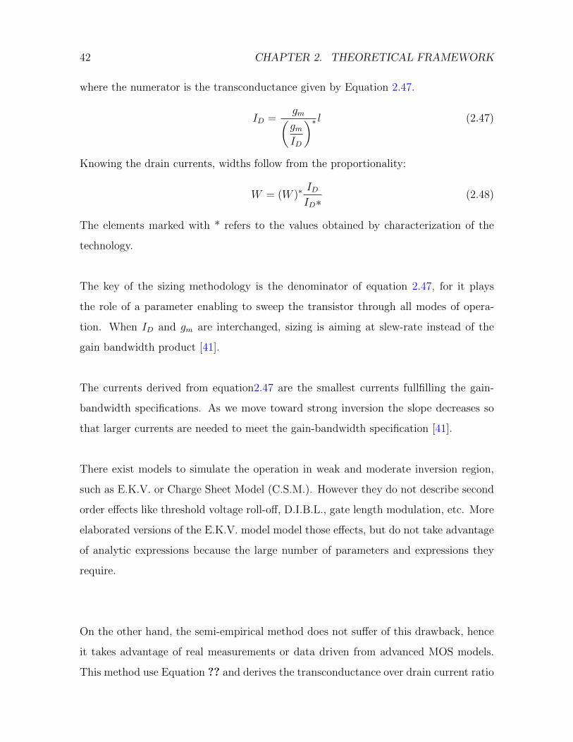
42 CHAPTER 2. THEORETICAL FRAMEWORK
where the numerator is the transconductance given by Equation 2.47.
ID =gm(gmID
)∗ l (2.47)
Knowing the drain currents, widths follow from the proportionality:
W = (W )∗IDID∗
(2.48)
The elements marked with * refers to the values obtained by characterization of the
technology.
The key of the sizing methodology is the denominator of equation 2.47, for it plays
the role of a parameter enabling to sweep the transistor through all modes of opera-
tion. When ID and gm are interchanged, sizing is aiming at slew-rate instead of the
gain bandwidth product [41].
The currents derived from equation2.47 are the smallest currents fullfilling the gain-
bandwidth specifications. As we move toward strong inversion the slope decreases so
that larger currents are needed to meet the gain-bandwidth specification [41].
There exist models to simulate the operation in weak and moderate inversion region,
such as E.K.V. or Charge Sheet Model (C.S.M.). However they do not describe second
order effects like threshold voltage roll-off, D.I.B.L., gate length modulation, etc. More
elaborated versions of the E.K.V. model model those effects, but do not take advantage
of analytic expressions because the large number of parameters and expressions they
require.
On the other hand, the semi-empirical method does not suffer of this drawback, hence
it takes advantage of real measurements or data driven from advanced MOS models.
This method use Equation ?? and derives the transconductance over drain current ratio
2.11. CMRR ENHACEMENT TECHNIQUE 43
from experimental ID(VGS characteristics.
The gm/ID ratio controls gain and power consumption, the larger gm/ID, the drain
current is reduced and the gain increased. This sizing methodology only applies how-
ever as long as channel widths are large enough to ignore lateral effects, a condition
that holds true with most CMOS analog circuits [41].
(gmID
) =1
I∗D
dI∗DdVG
=d
dVGlog(I∗D) (2.49)
Next chapter presents the proposal of this work and the design methodology description
for each block.
2.11 CMRR Enhacement Technique
An important aspect of the differential amplifier is its ability to reject a common signal
applied to both inputs. Often, in analog systems, signal are transmitted differentially,
and their ability to reject coupled noise into each line is very desirable.
The Common Mode Rejection Ratio (CMRR) is a parameter of differential amplifiers,
which may be severely affected when supply voltages become reduced. In the case of
an op-amp, it is calculated in the same way as in differential amplifiers. The common
mode gain of the differential amplifier is Ac, in the case of the op-amp isAcA2, and the
open loop differential gain of the op-amp is AOL(f) = AdA2, where A2 is the gain of
the second stage. The CMRR of the op-amp in dB is then given by equation 2.50 [6].
CMRR = 20logAOL(f)
AcA2
= 20logAd
Ac(2.50)
It is important to highlighted than the larger the CMRR, the better the performance
of the differential amplifier. So, in order to improve CMRR, the input of the ampli-
fier is designed to isolate the common mode input voltage from the rest of the circuit.
However, hence isolation will never be perfect, additional balancing is used to enhance

44 CHAPTER 2. THEORETICAL FRAMEWORK
the CMRR.
In the state of the art can be found two alternative approaches for the design of high
CMRR preamplifiers: resistive feedback and current feedback. The most significative
difference between these approaches resides on the way that high CMRR is obtained [4].
In the case of resistive feedback, a high CMRR requires a well balance resistor feed-
back network. On the other hand, current feedback uses both isolation and balancing
techniques to obtain the CMRR improvement.
For implementations based on resistive feedback can be found in literature three ap-
proaches, which are presented in Figure 2.11. The topology depicted in Figure 2.11 a),
is not well suitable for high-resistance sources, that problem can be solved by topology
depicted on Figure 2.11. b) However, that solution also amplifies the common-mode
voltage, as well as the differential voltage, and no improvement in the CMRR is ob-
tained. The most commonly used topology is shown in Figure 2.11 c) which major
advantage is a very high input resistance achieving and improvement in CMRR. The
input amplifiers act as a gain stage, while the other operates as a differential amplifier
with a typical unity gain value [4]. There exist different topologies to implement a
current feedback preamplifier, and their tradeoffs are presented in [4] with more details.
While resistive feedback techniques relies on balancing techniques and on-chip laser
trimming to achieve good performance, current feedback techniques use a combination
of isolation and balance techniques to obtain high CMRR and relatively good accu-
racy [4].
Due to the importance of high CMRR preamplifiers in several applications such biomed-
ical signal proccesing, new techniques to achieve that feature have been developed. One
proposed technique is presented in [36],and shown in Figure 2.12. Accordingly with [36],
only differential mode components of input voltages are applied to input transistors M1
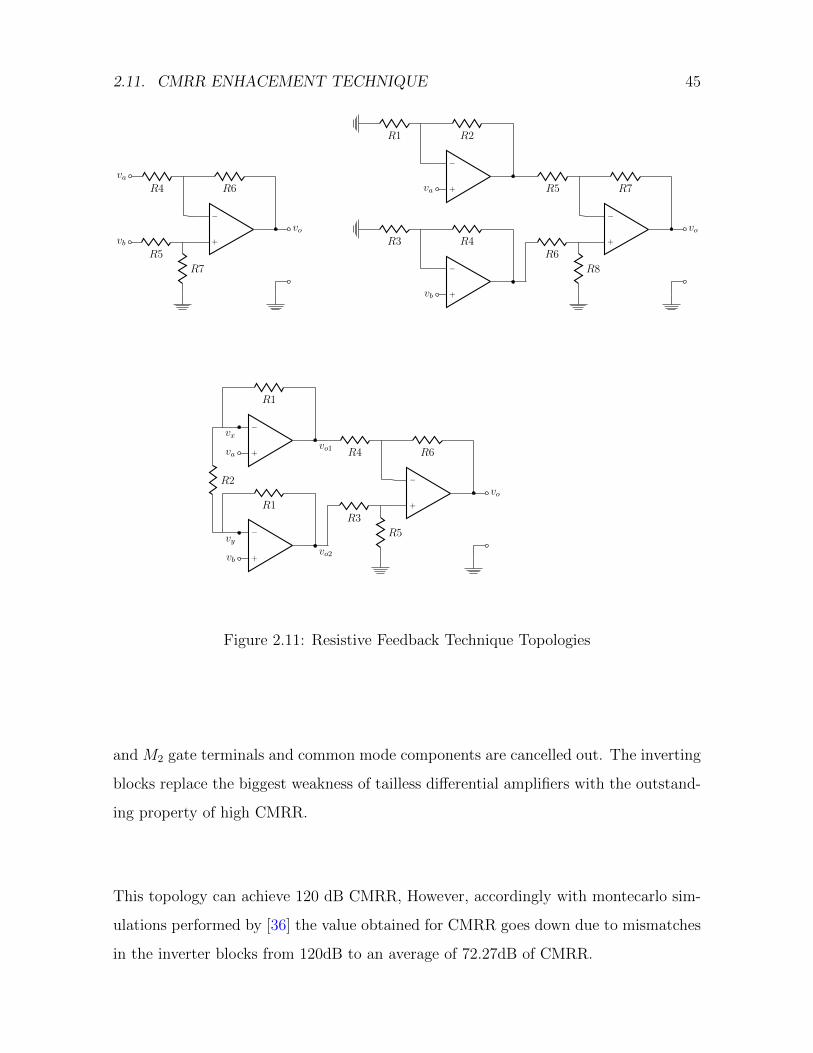
2.11. CMRR ENHACEMENT TECHNIQUE 45
−
+
vo
R6R4
va
R7
R5
vb
−
+
vo
R7R5
R8
R6
−
+
R2R1
va
−
+
R4R3
vb
−
+
vo
R6R4
R5
R3
−
+
R1
va
R2
vo1
vx
−
+
R1
vbvo2
vy
Figure 2.11: Resistive Feedback Technique Topologies
and M2 gate terminals and common mode components are cancelled out. The inverting
blocks replace the biggest weakness of tailless differential amplifiers with the outstand-
ing property of high CMRR.
This topology can achieve 120 dB CMRR, However, accordingly with montecarlo sim-
ulations performed by [36] the value obtained for CMRR goes down due to mismatches
in the inverter blocks from 120dB to an average of 72.27dB of CMRR.

46 CHAPTER 2. THEORETICAL FRAMEWORK
Figure 2.12: Topology presented in [36] for CMRR enhancement
2.12 Reduction of 1/f noise and Offset compensa-
tion techniques
Two of the most important phenomenons to deal with in analog integrated circuit de-
sign due to its implications and effects on circuits performance are noise and offset.
Immerse in literature can be found different techniques to overcome with these prob-
lems. It is well known than most techniques to remove flicker noise will also cancel
offset, and vice versa. Next, a comparative of these techniques will be presented.
a) Large Scale Excitation (LSE)
This is used to reduce 1/f noise. It consists on reset the memory of the system, com-
monly used in sensor circuits with low count of transistors or oscillators [37]. The main
disadvantages of this technique are the need of a sampled signal and that it cannot be
simulated or easily calculated.

2.12. REDUCTION OF 1/F NOISE ANDOFFSET COMPENSATION TECHNIQUES47
b) Trimming Techniques
It is an offset compensation technique based on the trimming of some elements of the
system . It needs unconventional CMOS processes, large voltages or currents and post
fabrication treatment, this leads to expensive fabrication cost and complexity, besides
that 1/f noise and dynamic offset are not compensated [38]. However it is not limited
to low bandwidths applications, the offset cancellation by itself dissipates no additional
power, it places minimal overhead on the amplifier design with non volatile storage of
offset reduction information. An example of this technique is presented in [13] which
uses floating gate transistors for correcting mismatches in analog circuitry, getting ad-
vantages as programmability, long term retention and can be fabricated in a standard
digital CMOS process. This approach involves no sampling and hence avoids such is-
sues as charge injection, clock feedthrough and undersampled wideband noise.
c) Correlated Double Sampling (CDS) and Auto-Zero(Az).
Those are sampled data techniques and its operating principle is trying to remove
flicker noise after it has occurred. First a sample without a signal is taken and then a
sample with a signal and subtract the two values ideally removing completely the offset
of the system and mostly flicker noise, nevertheless the white noise of the amplifier will
be doubled. For continuous time signals the result will be that flicker noise will not
disappear, instead a fold-over component will dominate at low frequencies. Moreover
AZ presents as disadvantage charge injection and switched noise effects, and Bandwidth
degradation.
For continuous time Auto-Zeroing such as ping pong technique, uses multiple amplifiers
and multi-phase clocks add additional overhead in terms of area and power.
Switched Capacitor comparator (SC) with CDS is a technique that present difficulties
48 CHAPTER 2. THEORETICAL FRAMEWORK
when switches open and inject parasitic charges.
There exist combinations of these techniques, as CDS with LSE, nevertheless the prob-
lem of this technique is that increasing the flicker noise instead of reducing it [37].
Typically the two methods to obtain the required cancellation of 1/f noise and off-
set are Chopper Stabilizaton and Auto Zero.
d) Stabilized Chopper.
Chopping can be used whenever it is possible to feed the signal through the flicker-
ing amplifier with different signs in every other clock period. This technique is based
on modulating the input up to frequencies fchop, 3fchop, 5fchop and so on. Then the
signal goes through the amplifier , where it picks flicker noise up and also offset. After
the amplifier the signal is demodulated to the base band, flicker noise and offset are
sent up to the multiples of fchop. So, as long as fchop is far enough above the signal
band, the signal is not disturbed by flicker noise. So, the chopper frequency must be
higher than the 1/f -noise corner frequency. In continuous time systems chopping will
not do any noise aliasing and, as the discrete case, it does not remove offset and flicker
noise. In this technique offset and gain specifications for the amplifier are important
issues, because the output signal saturate the following stages, resulting in the need of
a low pass filter after the second chopper. The main disadvantages of this technique
lies on design of the switches, because any charge injection will cause residual offset.
Such problems can be overcome using the nested chopper technique which uses two
chopper pairs, where an inner chopper is designed to move the 1/f noise out of the sig-
nal band. The outer chopper which operates at a lower frequency removes the residual
offset but the bandiwidth is degraded.
Therefore, Chopper technique disadvantages include complexity, besides it requires pas-
2.12. REDUCTION OF 1/F NOISE ANDOFFSET COMPENSATION TECHNIQUES49
sive filters which are hard to integrate.
LSE is used in sensor circuits with a low transistor count or in oscillators to reduce
1/f noise. In addition to the disadvantages mentioned before, this technique cannot be
simulated and design can be also difficult.
CDS is a technique commonly used in systems for sampled data, so Chopping is mostly
used in continuous time systems [37].
The main characteristics of each mentioned technique is shown in Table1.3, which
describes qualitatively and quantitatively the design tradeoffs of the different offset
cancellation and 1/f noise reduction techniques.

50 CHAPTER 2. THEORETICAL FRAMEWORK

Chapter 3
Design and Simulation Results of
the Preamplifier
3.1 Line Up Description
Biological System
Transducer
Preamp Filter
Analog Preprocessing Blocks
Signal Processor Output Signal
Electrical Signal
Figure 3.1: Block diagram of a processing biomedical signal acquisition system.
Figure 3.1 represents the block diagram of a biomedical system. It can be observed
the preprocessing block which consists of a preamplifier and a filter whose design is
the main purpose of this work. In order to obtain a good overall performance, some
blocks characteristics such as very low voltage or current noise, low harmonic distortion
components, low power consumption and minimum die area. In the case of the pream-
plifier, a high input impedance and high CMRR are also important, while a good DR
and quality factor (Q) are desirables in the case of the filters.
51

52CHAPTER 3. DESIGN AND SIMULATION RESULTS OF THE PREAMPLIFIER
−
+−
+Offset
Compensation
Outn∑
β
VpCMRR
Enhancement
Outp
-
+++
-
+++
∑
β
Vn
Figure 3.2: Preamplifier block diagram of Figure 3.1
As presented in equations (1.1) and (1.2), the PSRR and CMRR parameters are in-
versely related with the offset voltage, the offset voltage reduction will increase both
of these parameters. Therefore, the preamplifier block consist of a low noise ampli-
fier, with a CMRR enhancement circuit and an offset compensation scheme, which is
presented in Figure 3.2.
3.2 FCC Amplifier
3.2.1 Design of the FCC Amplifier
The folded cascode topology provides a good balance between output voltage swing
and power consumption [2]. Input transistors operate in subthreshold region to achieve
high trasconductance efficiency (gm/ID) [25].

3.2. FCC AMPLIFIER 53
The topology of the Fully Differential FCC operational amplifier proposed in this work
is shown in Figure 3.3 (a), while the topology of the common mode feedback (CMFB) is
presented in 3.3 (b). In Tables 3.1 and 3.2 the sizing of these topologies are presented.
V oosp V oosn
M1 M2
M3b
M3a
VDD
M3bp
M3ap
VDD
M31bVb2
M31aVb1
VDD
M14
VDD
M33b
M33a
VDD
M8
M10
VDD
M9
M11
CMFB
VDD
M8
VSS
M15
VSS
M16
VSS
M12
VSS
M4
VSS
M6
M5
VCMFB2
VSS
M7
VCMFB1
M17
VSS
VDD
IbiasFCC
M13
Vop
CL
Von
CL
Cin
Voinvp
Cin
Vinn
(a)
(b)
Voinvn
Vinp
Cin
Cin
M401
M405
VDD
M402
M408
M410
Von M404
M407
VDD
M403
M409VCMFB1
M411VCMFB2
VSSVSS
Vop
M406
VDD
VCMFB
Figure 3.3: Folded Cascode Operational Amplifier. (a)Topology of the folded cascode
amplifier. (b)CMFB of the folded cascode amplifier.

54CHAPTER 3. DESIGN AND SIMULATION RESULTS OF THE PREAMPLIFIER
Table 3.1: Sizing of the Folded Cascode Amplifier of Figure 3.3(a).
Transistor W [µm] L[µm] Transistor W [µm] L[µm]
M1=M2 370.8 2.1 M8=M9 6.6 2.1
M31a=M31b 61.8 2.1 M10=M11=M12 6.6 12
M3ap 64.8 2.1 M13 13.2 2.1
M3bp 61.8 2.1 M14 15 2.1
M4=M5 6.6 12 M15=M16=M17 26.4 2.1
M6=M7 13.2 2.1 M3a=M3b 123.6 2.1
Table 3.2: Sizing of the CMFB circuit used in the FCC of Figure 3.3 (b).
Transistor W [µm] L [µm]
M401=M402=M403=M404 26.4 2.1
M405=M406=M407 6.6 12
M408=M409 13.2 0.6
M410=M411 6.6 12
In order to describe the design methodology, parameters in table 3.3 have been con-
sidered. Before starting with the design process, technology characterization of PMOS
and NMOS transistors has been performed, resulting the table 3.4 data. After such
characterization, the starting point for this design is a 10nV/√Hz spec. The gm/ID
equations used to perform the design are [45]:
ID =gm
(gm/ID)∗(3.1)
W = W ∗ IDID∗
(3.2)
From noise analysis performed by [46] it is known that cascode devices do not contribute
with noise. The noise of the amplifier refered back to the input is given by:
V n2i = 2
[V n2
1 +
(gm5
gm1
)2
V n23 +
(gm11
gm1
)2
V n112
](3.3)

3.2. FCC AMPLIFIER 55
Table 3.3: FCC Design Parameters.
n 1.5
UT 2mV
K 1.38JK−1
T 300K
Kn 113.8×−6 µA/V2
Kp 36.8×−6 µA/V2
Vn2 10nV/√Hz
Table 3.4: Technology characterization data.
Id∗ L∗ W∗ gm∗
PMOS 5µA 2.1µm 160µm 95µA/V
NMOS 0.5µA 2.1µm 10µm 10.7µA/V
if gm1 >> gm5,11 the previous equation is simplified.
V n21 =
16KT
3gm1
(3.4)
this equation gives the starting point to perform a design based on noise specifications.
1. gm1 =16KT
3V n2, designed to operate in subthreshold region, from gm1 specification,
W1,2 and L1,2 are calculated by gm/ID methodology.
2. gm1 >> gm5,11 designed to operate in strong inversion gm4,5 = gm10,11 based on
gm specification and expected current are sized by gm/ID.
3. φM = tan−1(
gm6,7
2πf0CoxW6,7L6,7
)M6 must be designed carefully, hence it determines
the phase margin of the circuit.
4. M8,9 do not require strict design requirements, so their have a minimum W.

56CHAPTER 3. DESIGN AND SIMULATION RESULTS OF THE PREAMPLIFIER
3.2.2 Simulation Results
This section shows the Folded Cascode Operational Amplifier behaviour. Figure 3.4
shows the FCC AC response with a voltage gain of 83.4dB, bandwidth of 226.7Hz and
gain bandwidth of 2.97MHz where the phase margin is 59.35o.
Figure 3.4: Frequency response of the FCC Amplifier of Figure 3.3
Next, Figure 3.5 presents the amplifier DC simulation results, obtained a systematic
offset of 39µV, an input swing of 200µV and an output swing of 2.34V. While Figure 3.6
presents the simulated CMRR value obtained by the folded cascode amplifier, achieving
a CMRR of 91.5dB from 10mHz up to 2.7kHz and 91.4dB for a frequency of 3kHz. This
simulation has been realized with a mismatch offset of 4.5mV, which correspond to one
standard deviation calculated with pelgrom model.

3.2. FCC AMPLIFIER 57
Figure 3.5: DC response of the FCC Amplifier of Figure 3.3
1m 10m 100m 1 10 100 1k 10k 100k 1M
30
40
50
60
70
80
90
100
CM
RR
[dB
]
Frequency [Hz]
CMRR=91.5dBVos=4.5mV
Figure 3.6: CMRR of the FCC Amplifier of Figure 3.3

58CHAPTER 3. DESIGN AND SIMULATION RESULTS OF THE PREAMPLIFIER
1m 10m 100m 1 10 100 1k 10k 100k 1M 10M 100M0
10
20
30
40
50
60P
SR
R [d
B]
Frequency [Hz]
PSRR- 55.4dB PSRR+ 55dB
Vos=4.5mV
Figure 3.7: PSRR of the FCC Amplifier of Figure 3.3
Figure 3.7 presents the positive and negative power supply rejection ratio simulations
of the FCC of Figure 3.3, exhibiting a PSRR+ of 55dB and a PSRR- of 55.4dB, with an
offset voltage of 4.5mV. Simulated performance parameters of the amplifier of Figure
3.3 are listed in Table 3.5.
The closed loop simulation performance of the Folded Cascode Amplifier is summarized
in Table 3.6.

3.2. FCC AMPLIFIER 59
Table 3.5: Characterization of the FCC amplifier
Block FCC Amplifier
Process Specification 0.5µm
Supply Voltage ±1.65V
Supply Current 11.6µA
Open Loop Gain 83.4dB
BW 226.78Hz
GBW 2.97MHz
CMRR @0.05Hz up to 100Hz 91.5dB (Vos=4.5mV)
PSRR+ @0.05Hz up to 100Hz 55dB
PSRR- @0.05Hz up to 100Hz 55.4dB
PM 55.45o
Output Resistance 42MΩ
Systematic Offset 38µV
ICMR 200µV
Output swing 2.34V
THD(@100Hz,@100mV), ACL=1 0.152%
Dynamic Range 44.36dB
Pdiss 364µW
Input Refered Noise (0.5-100Hz)1.21µVRMS
CL 10pF
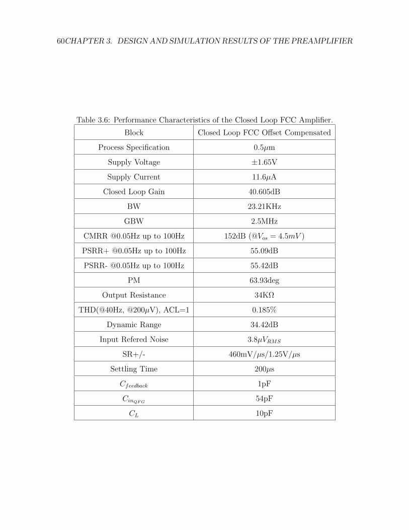
60CHAPTER 3. DESIGN AND SIMULATION RESULTS OF THE PREAMPLIFIER
Table 3.6: Performance Characteristics of the Closed Loop FCC Amplifier.
Block Closed Loop FCC Offset Compensated
Process Specification 0.5µm
Supply Voltage ±1.65V
Supply Current 11.6µA
Closed Loop Gain 40.605dB
BW 23.21KHz
GBW 2.5MHz
CMRR @0.05Hz up to 100Hz 152dB (@Vos = 4.5mV )
PSRR+ @0.05Hz up to 100Hz 55.09dB
PSRR- @0.05Hz up to 100Hz 55.42dB
PM 63.93deg
Output Resistance 34KΩ
THD(@40Hz, @200µV), ACL=1 0.185%
Dynamic Range 34.42dB
Input Refered Noise 3.8µVRMS
SR+/- 460mV/µs/1.25V/µs
Settling Time 200µs
Cfeedback 1pF
CinQFG54pF
CL 10pF
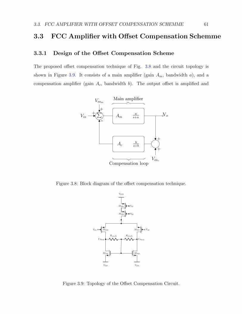
3.3. FCC AMPLIFIER WITH OFFSET COMPENSATION SCHEMME 61
3.3 FCC Amplifier with Offset Compensation Schemme
3.3.1 Design of the Offset Compensation Scheme
The proposed offset compensation technique of Fig. 3.8 and the circuit topology is
shown in Figure 3.9. It consists of a main amplifier (gain Am, bandwidth a), and a
compensation amplifier (gain Ac, bandwidth b). The output offset is amplified and
+
Vosc
Vo
+
∑-
Vosm
Vin+
+
Acbs+b
Amas+a
Main amplifier
Compensation loop
Figure 3.8: Block diagram of the offset compensation technique.
M32b
M32a
VDD
Vb1
Vb2
M103Von VopM104
M101 M102
VSS VSS
V oosp
Rcmfb Rcmfb
V oosn
Figure 3.9: Topology of the Offset Compensation Circuit.
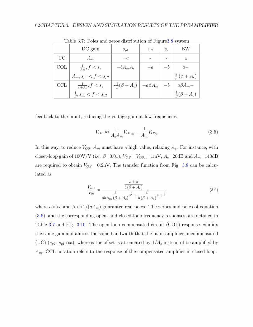
62CHAPTER 3. DESIGN AND SIMULATION RESULTS OF THE PREAMPLIFIER
Table 3.7: Poles and zeros distribution of Figure3.8 system
DC gain sp1 sp2 sz BW
UC Am −a - - a
COL 1AC, f < sz −bAmAc −a −b a−
Am, sp1 < f < sp2bβ
(β + Ac)
CCL 1β+Ac
, f < sz - bβ(β + Ac) −aβAm −b aβAm−
1β, sp1 < f < sp2
bβ(β + Ac)
feedback to the input, reducing the voltage gain at low frequencies.
VOS ≈1
AcAmVOSm −
1
AmVOSc (3.5)
In this way, to reduce VOS, Am must have a high value, relaxing Ac. For instance, with
closet-loop gain of 100V/V (i.e. β=0.01), VOSc=VOSm=1mV, Ac=20dB and Am=140dB
are required to obtain VOS =0.2nV. The transfer function from Fig. 3.8 can be calcu-
lated as
VoutVin
≈
s+ b
b (β +Ac)1
abAm (β +Ac)s2 +
β
b (β +Ac)s+ 1
(3.6)
where a>>b and β>>1/(aAm) guarantee real poles. The zeroes and poles of equation
(3.6), and the corresponding open- and closed-loop frequency responses, are detailed in
Table 3.7 and Fig. 3.10. The open loop compensated circuit (COL) response exhibits
the same gain and almost the same bandwidth that the main amplifier uncompensated
(UC) (sp2 -sp1 ≈a), whereas the offset is attenuated by 1/Ac instead of be amplified by
Am. CCL notation refers to the response of the compensated amplifier in closed loop.

3.3. FCC AMPLIFIER WITH OFFSET COMPENSATION SCHEMME 63
Figure 3.10: Frequency Responses of the system of Figure 3.8
Table 3.8 shows the sizing of the offset compensation scheme components, whoso where
designed as follows:
1. M103 =1
3M1 since this block does not require rigorous specification of design as
can be notice in equation 3.5 the offset voltage produced by this block will be
divided by the main amplifier (FCC) gain, so its design can be relaxing.
2. M101 = M102 This transistors has been sizing based on M103 to achieve a sym-
metric DC response of the amplifier.
Table 3.8: Sizing of the offset compensation circuit.
Transistor W [µm] L [µm] Device Value
M103=M104 184.3 2.1 RCMFB 200KΩ
M101=M102 6.6 18
M32a=M32b 123.6 2.1
Figure 3.11 represents the topology of the FCC Amplifier with offset compensation
circuit.

64CHAPTER 3. DESIGN AND SIMULATION RESULTS OF THE PREAMPLIFIER
M1 M2
M3b
M3a
VDD
M3bp
M3ap
VDD
M31bVb2
M31aVb1
VDD
M14
VDD
M33b
M33a
VDD
M8
M10
VDD
M9
M11
CMFB
VDD
M8
VSS
M15
VSS
M16
VSS
M12
VSS
M4
VSS
M6
M5
VCMFB2
VSS
M7
VCMFB1
M17
VSS
VDD
IbiasFCC
M13
Vop
CL
Von
CL
Cin
VinnVinp
Cin
Cin
OFFSET COMPENSATION SCHEME
M32b
M32a
VDD
Vb1
Vb2
M103Von VopM104
M101 M102
VSS VSS
V oospRcmfb Rcmfb
V oosn
Figure 3.11: FCC Amplifier with Offset Compensation Scheme.

3.3. FCC AMPLIFIER WITH OFFSET COMPENSATION SCHEMME 65
3.3.2 Simulation Results
Then, simulations of the FCC with offset compensation circuit and closed loop condition
are shown next. Starting with Figure 3.12, the frequency response is presented achieving
40dB of Gain, 23.2kHz of bandwidth and GBW of 2.49MHz with a phase margin of
64.3o.
Figure 3.12: Frequency Response of the FCC amplifier with Offset Compensation
Montecarlo analysis has been performed on Common Mode Rejection Ratio of the FCC
Amplifier with offset compensation of Figure 3.11, and results are depicted in Figure
3.13.
Besides, Monte Carlo analysis is performed in order to notice offset variations in this
FCC with offset compensation topology, see Figure 3.14, where a standard deviation of
104nV is obtained.

66CHAPTER 3. DESIGN AND SIMULATION RESULTS OF THE PREAMPLIFIER
Figure 3.13: CMRR of the FCC amplifier with Offset Compensation
Figure 3.14: Offset of the FCC amplifier with Offset Compensation
3.4. FCC AMPLIFIER WITH CMRR ENHANCEMENT CIRCUIT 67
3.4 FCC Amplifier with CMRR Enhancement Cir-
cuit
3.4.1 Design of the CMRR Enhancement Circuit
M201 M202
Rb Rb
VinnVinp
Rb Rb
M203 M204
RCMFB RCMFB
V oinvn V oinvp
VSS VSS
M34b
M34a Vb1
Vb2
VDD
Figure 3.15: Topology of the CMRR Enhancement Circuit.
Table 3.9: Sizing of the CMRR enhancement circuit.
Transistor W [µm] L [µm] Device Value
M201=M202 185.4 2.1 RCMFB 200KΩ
M203=M204 6.6 18 Rb 100KΩ
M34a=M34b 123.6 2.1
The CMRR enhancement block has been based on topology presented by [36] and cited
in chapter 2. This topology, shown in Figure 3.15, is based on a differential amplifier,
Quasi Floating gates transistors and two inverters. In this work will such amplifier be
designed to achieve a stable unity gain through a resistive network, because the high
performance of this technique depends on the inverter block unity gain. The CMRR
improvement of the circuit will be established by:
CMRR =
(V QFGdm
V QFGcm
)(VCMVdm/2
)(3.7)
68CHAPTER 3. DESIGN AND SIMULATION RESULTS OF THE PREAMPLIFIER
The sizing of table 3.9 were obtained as follows:
1. M201 = M202 =1
3M1,2 as in offset compensation scheme.
2. M203 = M204 are sizing based on M201 to achieve a symmetric DC response of the
amplifier.
3. All these resistances Rb have the same value to achieve an unity gain amplifier
which gain does not depends on mismatch transistor, which is the main disad-
vantage of [36].
Figure 3.16 presents the topology of the FCC Amplifier with CMRR Enhancement
Circuit.
M1 M2
M3b
M3a
VDD
M3bp
M3ap
VDD
M31bVb2
M31aVb1
VDD
M14
VDD
M33b
M33a
VDD
M8
M10
VDD
M9
M11
CMFB
VDD
M8
VSS
M15
VSS
M16
VSS
M12
VSS
M4
VSS
M6
M5
VCMFB2
VSS
M7
VCMFB1
M17
VSS
VDD
IbiasFCC
M13
Vop
CL
Von
CL
Cin
Voinvp
Cin
Vinn
Voinvn
Vinp
Cin
Cin
M201 M202
Rb Rb VinnVinp
Rb Rb
M203 M204
RCMFB RCMFB
VSS VSS
M34b
M34a Vb1
Vb2
VDD
CMRR ENHANCEMENT CIRCUIT
Figure 3.16: FCC Amplifier with CMRR Enhancement Circuit

3.4. FCC AMPLIFIER WITH CMRR ENHANCEMENT CIRCUIT 69
3.4.2 Simulation Results
Now, simulations of the FCC with Common Mode Rejection Ratio Enhancement Circuit
of Figure 3.16 are presented. Frequency response of FCC with CMRR enhancement
technique is depicted in Figure 3.17 with performance values of 39.9dB of gain, 27.3kHz
of BW and 2.7MHz of GBW with 58.73o of phase margin. The mean value 0f 106dB
of CMRR is depicted in Figure 3.18 with a standard deviation of 106dB of CMRR.
Figure 3.17: Frequency Response of the FCC amplifier with CMRR Enhancement Cir-
cuit
Figure 3.19 presents the simulated behaviour of the input referred offset through one
hundred iterations of monte carlo analysis, which results in 1.5V of offset variations.
Therefore, even when the dispersion of the CMRR is lower than in previous implemen-
tation, the reached up values are smaller and the offset variations are severely increased.

70CHAPTER 3. DESIGN AND SIMULATION RESULTS OF THE PREAMPLIFIER
[!t]
Figure 3.18: CMRR of the FCC amplifier with CMRR Enhancement Circuit
Figure 3.19: Offset of the FCC amplifier with CMRR Enhancement Circuit

3.5. FCC AMPLIFIERWITH OFFSET COMPENSATION SCHEMEAND CMRR ENHANCEMENT CIRCUIT71
3.5 FCC Amplifier with Offset Compensation Scheme
and CMRR Enhancement Circuit
3.5.1 Topology
Figure 3.20 represents the topology of the FCC Amplifier with both techniques imple-
mented, Offset Compensation and CMRR Enhancement.
M1 M2
M3b
M3a
VDD
M3bp
M3ap
VDD
M31bVb2
M31aVb1
VDD
M14
VDD
M33b
M33a
VDD
M8
M10
VDD
M9
M11
CMFB
VDD
M8
VSS
M15
VSS
M16
VSS
M12
VSS
M4
VSS
M6
M5
VCMFB2
VSS
M7
VCMFB1
M17
VSS
VDD
IbiasFCC
M13
Vop
CL
Von
CL
Cin
Voinvp
Cin
Vinn
Voinvn
Vinp
Cin
Cin
M201 M202
Rb Rb VinnVinp
Rb Rb
M203 M204
RCMFB RCMFB
VSS VSS
M34b
M34a Vb1
Vb2
VDD
CMRR ENHANCEMENT CIRCUIT
OFFSET COMPENSATION SCHEME
M32b
M32a
VDD
Vb1
Vb2
M103Von VopM104
M101 M102
VSS VSS
V oospRcmfb Rcmfb
V oosn
Figure 3.20: FCC Amplifier with Offset Compensation Scheme and CMRR Enhance-
ment Circuit.

72CHAPTER 3. DESIGN AND SIMULATION RESULTS OF THE PREAMPLIFIER
3.5.2 Simulation Results
Plots of the FCC simulations with both techniques implemented at the same time, as
presented in Figure 3.20 are shown next. Figure 3.21 presents the frequency response of
this implementation, with a gain of 39.9dB, BW of 22.4kHz, GBW of 2.3MHz and phase
margin of 67.1o. Next, a 112dB of CMRR simulation is depicted in Figure 3.22 along
with its 100 hundred iterations of Monte Carlo analysis, where the CMRR is ranging
from 112dB up to 150dB. simulations. Figure 3.23 shows offset variations perform-
ing by one hundred iterations in Monte Carlo simulations, resulting in 3mV of offset
variations. Although this third implementation presents the smallest offset variation,
the first implementation which correspond to the FCC with the offset compensation,
presents the best CMRR performance and similar offset compensation behaviour.
Figure 3.21: Frequency Response of the FCC amplifier with CMRR Enhancement Cir-
cuit and Offset Compensation Scheme

3.5. FCC AMPLIFIERWITH OFFSET COMPENSATION SCHEMEAND CMRR ENHANCEMENT CIRCUIT73
Figure 3.22: CMRR of the FCC amplifier with CMRR Enhancement Circuit
Figure 3.23: Offset of the FCC amplifier with CMRR Enhancement Circuit and Offset
Compensation Scheme
74CHAPTER 3. DESIGN AND SIMULATION RESULTS OF THE PREAMPLIFIER
3.6 Comparison
Figure 3.24 shows a comparison of the CMRR performance of the different approaches
of the FCC where can be appreciated than the first approach presents the best CMRR
performance.
Figure 3.24: CMRR performance comparison of the FCC

Chapter 4
Tunable Filters
4.1 Design and Simulatin Results of the High Value
Tunable Resistor
Table 4.1: Designed Values for the HVTR of Figure 4.1.
Device W/L [µm/µm]
M1 6/1.2
M2 6/1.2
M3 6/1.2
M4 6/1.2
Ca 0.05pF
This implementation is characterized by a moderate swing (Vswing > VTH), because
large voltage variations in the control voltage (Vc) drives transistors into saturation
region, turning on the reverse biased junctions, reducing dramatically their resistance
and leading to a non linear behaviour.
75
76 CHAPTER 4. TUNABLE FILTERS
As mentioned in previous chapter, dimensions for PMOS transistors must be minimum-
sized in order to reduce area requirements. In this topology, each transistor bulk must
be connected to its own source, to allow high resistive performance. In Figure 4.2 is pre-
Ca Ca
Vc
A BMp1 Mp2 Mp3
Mp4
Figure 4.1: Topology of the High Voltage Tunable Resistor.
sented the DC simulation result of the HVTR with a control voltage sweep from −0.6V
to −0.2V with a step of 10mV. As can be seen the linear behaviour of the HVTR is
extremely reduced in a range of −0.33V to −0.28V where the resistor can vary from
105GΩ to 243GΩ. It is important to mention that this simulation was performed with
a 1V voltage source VAB connected between terminals A and B of the resistor. If we
connect one of the HVTR terminals to a fixed voltage and the other one to ground,
the resistance could be different. Since the resistance value provided by the HVTR is
dependent on its terminals voltage, what is very important to take into account during
the design process.
Figure 4.3 shows the behaviour of the HVTR, at different control voltages (Vc) with a
voltage VAB of 1V. From this Figure it can be observe the linear range of this resistance
which depends on the control voltage.
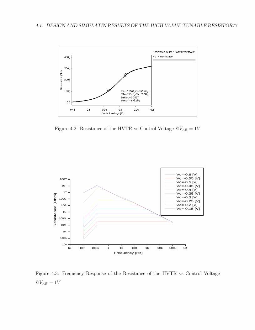
4.1. DESIGN AND SIMULATIN RESULTS OF THE HIGH VALUE TUNABLE RESISTOR77
Figure 4.2: Resistance of the HVTR vs Control Voltage @VAB = 1V
1m 10m 100m 1 10 100 1k 10k 100k 1M10k
100k
1M
10M
100M
1G
10G
100G
1T
10T
100T
Res
ista
nce
[Ohm
]
Frequency [Hz]
Vc=-0.6 [V] Vc=-0.55 [V] Vc=-0.5 [V] Vc=-0.45 [V] Vc=-0.4 [V] Vc=-0.35 [V] Vc=-0.3 [V] Vc=-0.25 [V] Vc=-0.2 [V] Vc=-0.15 [V]
Figure 4.3: Frequency Response of the Resistance of the HVTR vs Control Voltage
@VAB = 1V
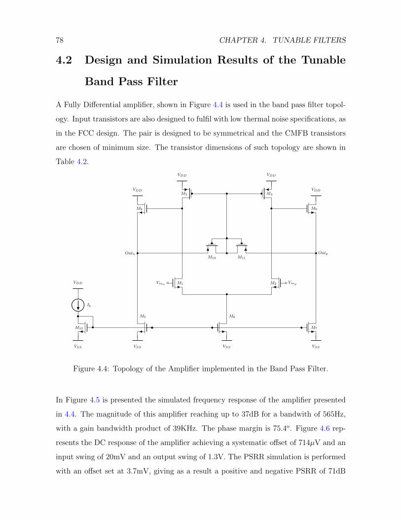
78 CHAPTER 4. TUNABLE FILTERS
4.2 Design and Simulation Results of the Tunable
Band Pass Filter
A Fully Differential amplifier, shown in Figure 4.4 is used in the band pass filter topol-
ogy. Input transistors are also designed to fulfil with low thermal noise specifications, as
in the FCC design. The pair is designed to be symmetrical and the CMFB transistors
are chosen of minimum size. The transistor dimensions of such topology are shown in
Table 4.2.
M1 M2
M3 M4
M10 M11
M8 M9
M6
VDD VDD
VDD VDD
M5
M7
VSS VSS VSS
M12
Ib
VDD
VSS
VinnVinp
Outn Outp
Figure 4.4: Topology of the Amplifier implemented in the Band Pass Filter.
In Figure 4.5 is presented the simulated frequency response of the amplifier presented
in 4.4. The magnitude of this amplifier reaching up to 37dB for a bandwith of 565Hz,
with a gain bandwidth product of 39KHz. The phase margin is 75.4o. Figure 4.6 rep-
resents the DC response of the amplifier achieving a systematic offset of 714µV and an
input swing of 20mV and an output swing of 1.3V. The PSRR simulation is performed
with an offset set at 3.7mV, giving as a result a positive and negative PSRR of 71dB

4.2. DESIGN AND SIMULATION RESULTS OF THE TUNABLE BAND PASS FILTER79
Table 4.2: Transistors Sizing of the Amplifier of Figure 4.4.
Transistor W/L [µm/µm]
M1 = M2 12/1.2
M5 = M6 = M7 12/1.2
M8 = M9 12/1.2
M3 = M4 36/1.2
M10 = M11 6/1.2
Figure 4.5: Frequency Response of the Amplifier of the Band Pass Filter.
and 70dB respectively as presented in 4.7. On the other hand a 89.5dB of CMRR is
obtained as depicted in Figure 4.8, this simulations have been performed with an offset
of 3.7mV.

80 CHAPTER 4. TUNABLE FILTERS
Figure 4.6: DC Response
10m 100m 1 10 100 1k 10k 100k 1M 10M 100M 1G
-20
0
20
40
60
80
PS
RR
[dB
]
Frequency [Hz]
PSRR+ (71dB) PSRR- (70 dB)
Voff=3.7mV
Figure 4.7: Analysis of Power Supply Rejection Ratio of the Amplifier of Band Pass
Filter.

4.2. DESIGN AND SIMULATION RESULTS OF THE TUNABLE BAND PASS FILTER81
100m 1 10 100 1k 10k 100k 1M30
40
50
60
70
80
90C
MR
R [d
B]
Frequency [Hz]
CMRR=89.5dB Vos=3.7mV
Figure 4.8: Analysis of the Common Mode Rejection Ratio of the Amplifier of Band
Pass Filter.
The slew rate simulation is depicted in 4.9, this simulation has been performed with
the amplifier in closed loop and a load capacitance of 1pF, resulting in a positive slew
rate of 46V/µs and negative of 47V/µs. An important characteristic of this topology
is presented in Figure 4.10 where is presented the behaviour in time of the load ca-
pacitor current. As can be observed the amplifier is able to give the necessary current
as much as the requirements of the load demand it, up to 50µA. Taking into account
that the bias current of this amplifier is 25nA. Table 4.3 summarizes tha simulated
characterization of the amplifier of Figure 4.4.

82 CHAPTER 4. TUNABLE FILTERS
-250,00n 0,00 250,00n 500,00n 750,00n 1,00µ 1,25µ
-1,5
-1,0
-0,5
0,0
0,5
1,0
1,5V
olta
ge [V
]
Time [s]
Vin Vout
SR+=46V/usSR-=47V/usCL=1pF@Av=1(Closed Loop)
Figure 4.9: Slew Rate of the Amplifier of Band Pass Filter.
0,0 500,0n 1,0µ 1,5µ 2,0µ-80,0µ
-60,0µ
-40,0µ
-20,0µ
0,0
20,0µ
40,0µ
60,0µ
Load
Cap
acito
r Cur
rent
[A]
Time [s]
Figure 4.10: Current of the BPF Amplifier

4.2. DESIGN AND SIMULATION RESULTS OF THE TUNABLE BAND PASS FILTER83
Table 4.3: Performance Characteristics of the BPF Amplifier
Block BPF Amplifier
Process Specification 0.5µm
Supply Voltage ±1.65V
Supply Current 25nA
Open Loop Gain 37dB
BW 565Hz
GBW 39KHz
CMRR @100Hz 89.5dB
PSRR+ @100Hz 71dB
PSRR-@100Hz 70dB
PM 75.4deg
Output Resistance 260KΩ
Systematic Offset 714µV
ICMR 20mV
Output Swing 1.3V
THD(@100mV), ACL=1 @100Hz (0.56%)
Dynamic Range 66.95dB
SR+/- 46V/µs/47V/µs
Settling Time 100µs
Pdiss 247.5nW
CL 1pF
Layout Area 56.7µm × 79µm
Input Refered Noise 44.89µVRMS
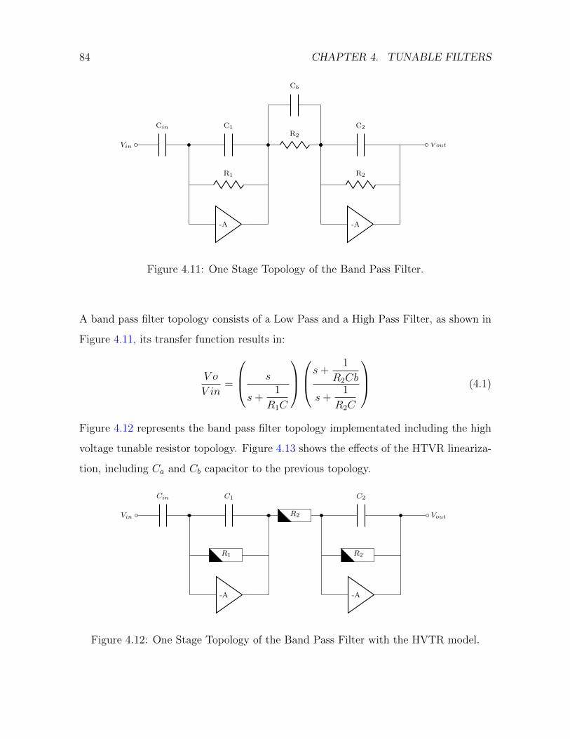
84 CHAPTER 4. TUNABLE FILTERS
Vin
Cin C1
R1
-A
R2
Cb
C2
V out
R2
-A
Figure 4.11: One Stage Topology of the Band Pass Filter.
A band pass filter topology consists of a Low Pass and a High Pass Filter, as shown in
Figure 4.11, its transfer function results in:
V o
V in=
s
s+1
R1C
s+
1
R2Cb
s+1
R2C
(4.1)
Figure 4.12 represents the band pass filter topology implementated including the high
voltage tunable resistor topology. Figure 4.13 shows the effects of the HTVR lineariza-
tion, including Ca and Cb capacitor to the previous topology.
Vin
Cin C1
R1
-A
R2
C2
Vout
R2
-A
Figure 4.12: One Stage Topology of the Band Pass Filter with the HVTR model.
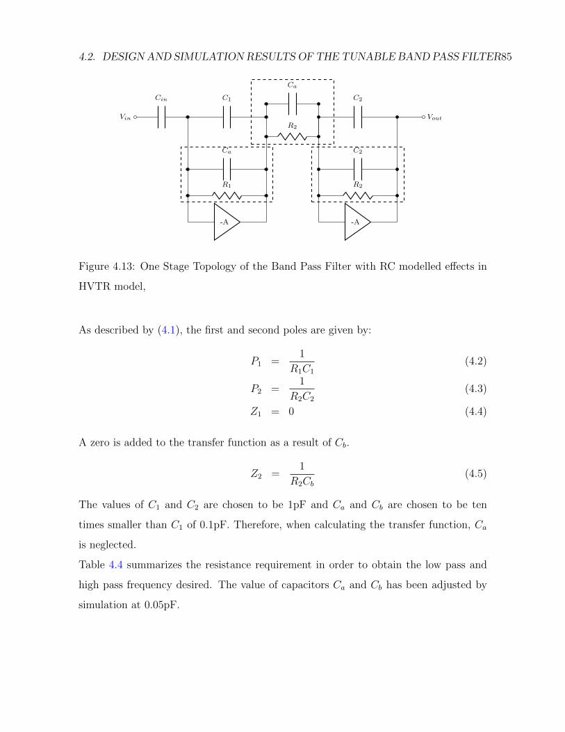
4.2. DESIGN AND SIMULATION RESULTS OF THE TUNABLE BAND PASS FILTER85
Vin
Cin C1
R1
Ca
-A
R2
Ca
C2
Vout
R2
C2
-A
Figure 4.13: One Stage Topology of the Band Pass Filter with RC modelled effects in
HVTR model,
As described by (4.1), the first and second poles are given by:
P1 =1
R1C1
(4.2)
P2 =1
R2C2
(4.3)
Z1 = 0 (4.4)
A zero is added to the transfer function as a result of Cb.
Z2 =1
R2Cb(4.5)
The values of C1 and C2 are chosen to be 1pF and Ca and Cb are chosen to be ten
times smaller than C1 of 0.1pF. Therefore, when calculating the transfer function, Ca
is neglected.
Table 4.4 summarizes the resistance requirement in order to obtain the low pass and
high pass frequency desired. The value of capacitors Ca and Cb has been adjusted by
simulation at 0.05pF.

86 CHAPTER 4. TUNABLE FILTERS
Cin
Cin
C1
C1
-
+
+
-
Vcp1
Rg1
Vcp1
Rg1
V inn
V inp
Vcp2
Rg2
Vcp2
Rg2
(b)
C2
C2
-
+
+
-
Vcp2
Rg2
Vcp2
Rg2
Vinn
Vinp
BPF
(a)
BPF BPF
Vout+
Vout-
Figure 4.14: Topology of the Band Pass Filter. (a)Three-stages block diagram of the
BPF. (b)One stage topology of the BPF.
Table 4.4: Resistor’s Value for the Band Pass Filter for the different biomedical band.
Band Low − pass freq. High− pass freq. Resistance Resistance
fL[Hz] FH [Hz] R1[Ω] R2 [Ω]
ECG 0.05 100 3.2 T 1.6 G
EEG 0.2 100 795 G 1.6 G
EMG 50 3 K 3.2 G 53 M
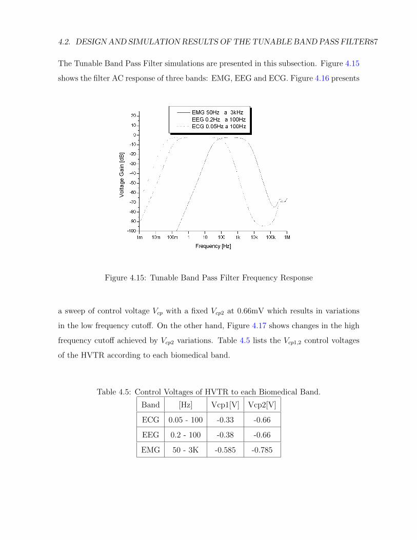
4.2. DESIGN AND SIMULATION RESULTS OF THE TUNABLE BAND PASS FILTER87
The Tunable Band Pass Filter simulations are presented in this subsection. Figure 4.15
shows the filter AC response of three bands: EMG, EEG and ECG. Figure 4.16 presents
Figure 4.15: Tunable Band Pass Filter Frequency Response
a sweep of control voltage Vcp with a fixed Vcp2 at 0.66mV which results in variations
in the low frequency cutoff. On the other hand, Figure 4.17 shows changes in the high
frequency cutoff achieved by Vcp2 variations. Table 4.5 lists the Vcp1,2 control voltages
of the HVTR according to each biomedical band.
Table 4.5: Control Voltages of HVTR to each Biomedical Band.
Band [Hz] Vcp1[V] Vcp2[V]
ECG 0.05 - 100 -0.33 -0.66
EEG 0.2 - 100 -0.38 -0.66
EMG 50 - 3K -0.585 -0.785
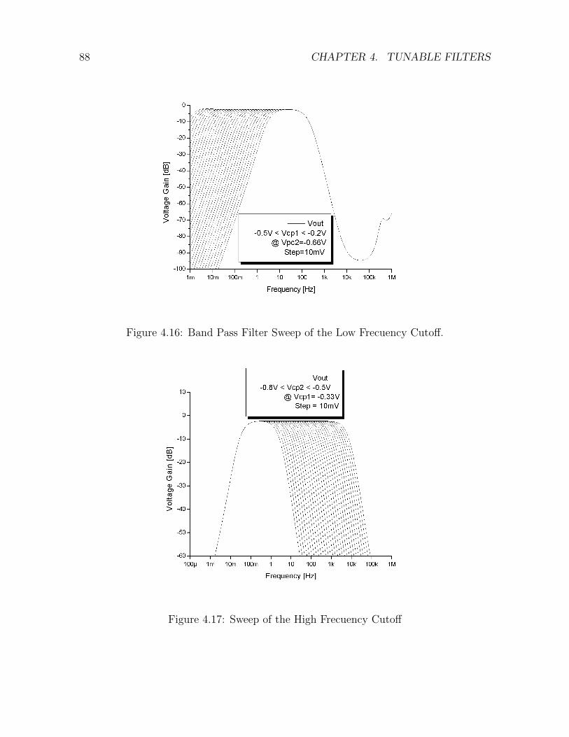
88 CHAPTER 4. TUNABLE FILTERS
Figure 4.16: Band Pass Filter Sweep of the Low Frecuency Cutoff.
Figure 4.17: Sweep of the High Frecuency Cutoff

4.2. DESIGN AND SIMULATION RESULTS OF THE TUNABLE BAND PASS FILTER89
Table 4.6: Performance parameters of the band pass filter obtained by simulation for
different bandwidths.
@200mV 80Hz BW IRN THD @fmidband DR
ECG 0.05Hz a 100Hz 266µVrms 2.52% 57.5dB
EEG 0.2Hz a 100Hz 254µVrms 2.51% 57.9dB
EMG 50Hz a 3KHz 193.4µVrms 1.49% 60.3dB
In regard to distortion, Figure 4.18 shows the second and third Harmonic Distortion
Percentage for the biomedical bands.
Then, Table 4.6 lists the band pass filter performance parameters obtained by simu-
lation. The layout realization of the Band Pass Filter is presented in Figure 4.19.
25,00m 50,00m 75,00m 100,00m 125,00m 150,00m 175,00m 200,00m
0,20,40,60,81,01,21,41,61,82,02,22,4
HD2 EMG HD3 EMG HD2 EEG HD3 EEG HD2 ECG HD3 ECG
Har
mon
ic D
isto
rtion
[%]
Input Signal Amplitude [V]
Figure 4.18: Second and third Harmonic Distortion Percentage of the Band Pass Filter.
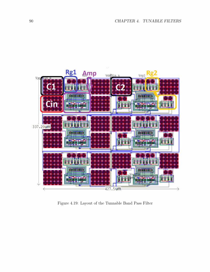
90 CHAPTER 4. TUNABLE FILTERS
Figure 4.19: Layout of the Tunnable Band Pass Filter
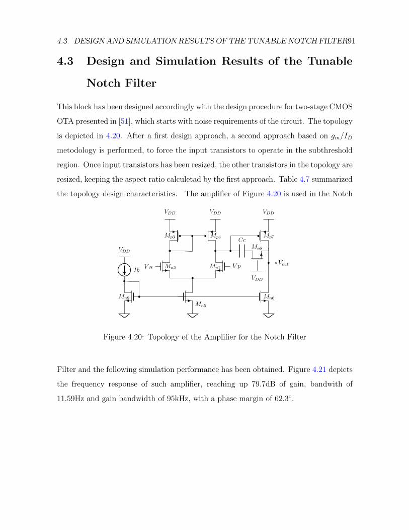
4.3. DESIGN AND SIMULATION RESULTS OF THE TUNABLE NOTCH FILTER91
4.3 Design and Simulation Results of the Tunable
Notch Filter
This block has been designed accordingly with the design procedure for two-stage CMOS
OTA presented in [51], which starts with noise requirements of the circuit. The topology
is depicted in 4.20. After a first design approach, a second approach based on gm/ID
metodology is performed, to force the input transistors to operate in the subthreshold
region. Once input transistors has been resized, the other transistors in the topology are
resized, keeping the aspect ratio calculetad by the first approach. Table 4.7 summarized
the topology design characteristics. The amplifier of Figure 4.20 is used in the Notch
Mn1 V pMn2V n
Mn5
Mn9
Ib
VDD
Mp4Mp3
VDD VDD
CcMn8
VDD
Mp7
VDD
Vout
Mn6
Figure 4.20: Topology of the Amplifier for the Notch Filter
Filter and the following simulation performance has been obtained. Figure 4.21 depicts
the frequency response of such amplifier, reaching up 79.7dB of gain, bandwith of
11.59Hz and gain bandwidth of 95kHz, with a phase margin of 62.3o.
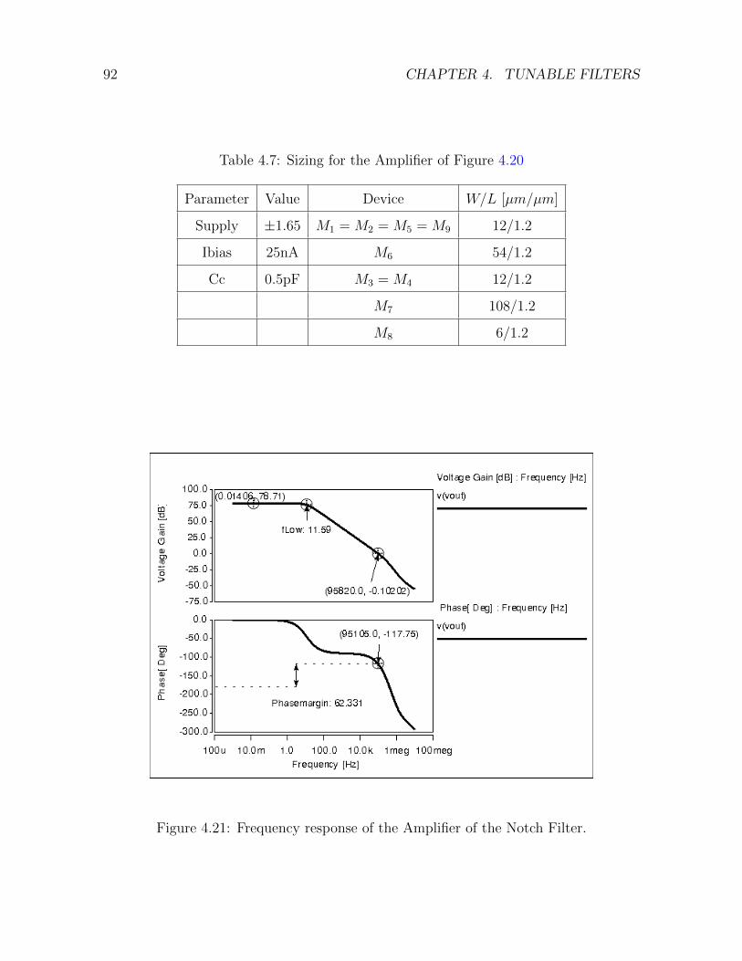
92 CHAPTER 4. TUNABLE FILTERS
Table 4.7: Sizing for the Amplifier of Figure 4.20
Parameter Value Device W/L [µm/µm]
Supply ±1.65 M1 = M2 = M5 = M9 12/1.2
Ibias 25nA M6 54/1.2
Cc 0.5pF M3 = M4 12/1.2
M7 108/1.2
M8 6/1.2
Figure 4.21: Frequency response of the Amplifier of the Notch Filter.
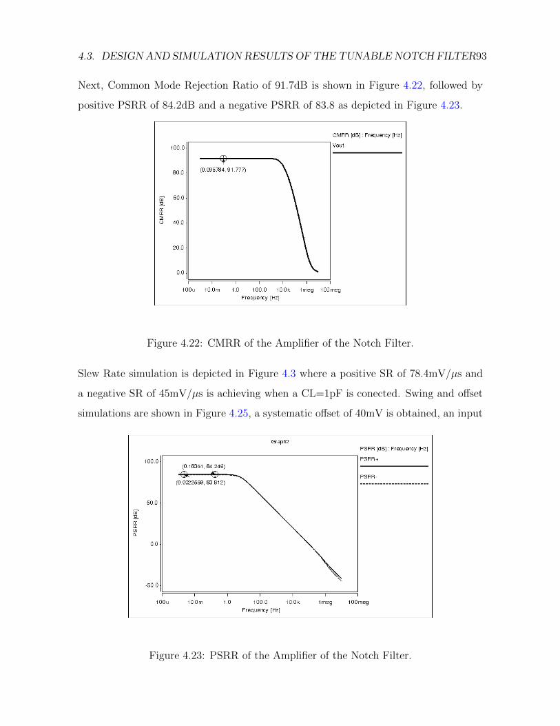
4.3. DESIGN AND SIMULATION RESULTS OF THE TUNABLE NOTCH FILTER93
Next, Common Mode Rejection Ratio of 91.7dB is shown in Figure 4.22, followed by
positive PSRR of 84.2dB and a negative PSRR of 83.8 as depicted in Figure 4.23.
Figure 4.22: CMRR of the Amplifier of the Notch Filter.
Slew Rate simulation is depicted in Figure 4.3 where a positive SR of 78.4mV/µs and
a negative SR of 45mV/µs is achieving when a CL=1pF is conected. Swing and offset
simulations are shown in Figure 4.25, a systematic offset of 40mV is obtained, an input
Figure 4.23: PSRR of the Amplifier of the Notch Filter.
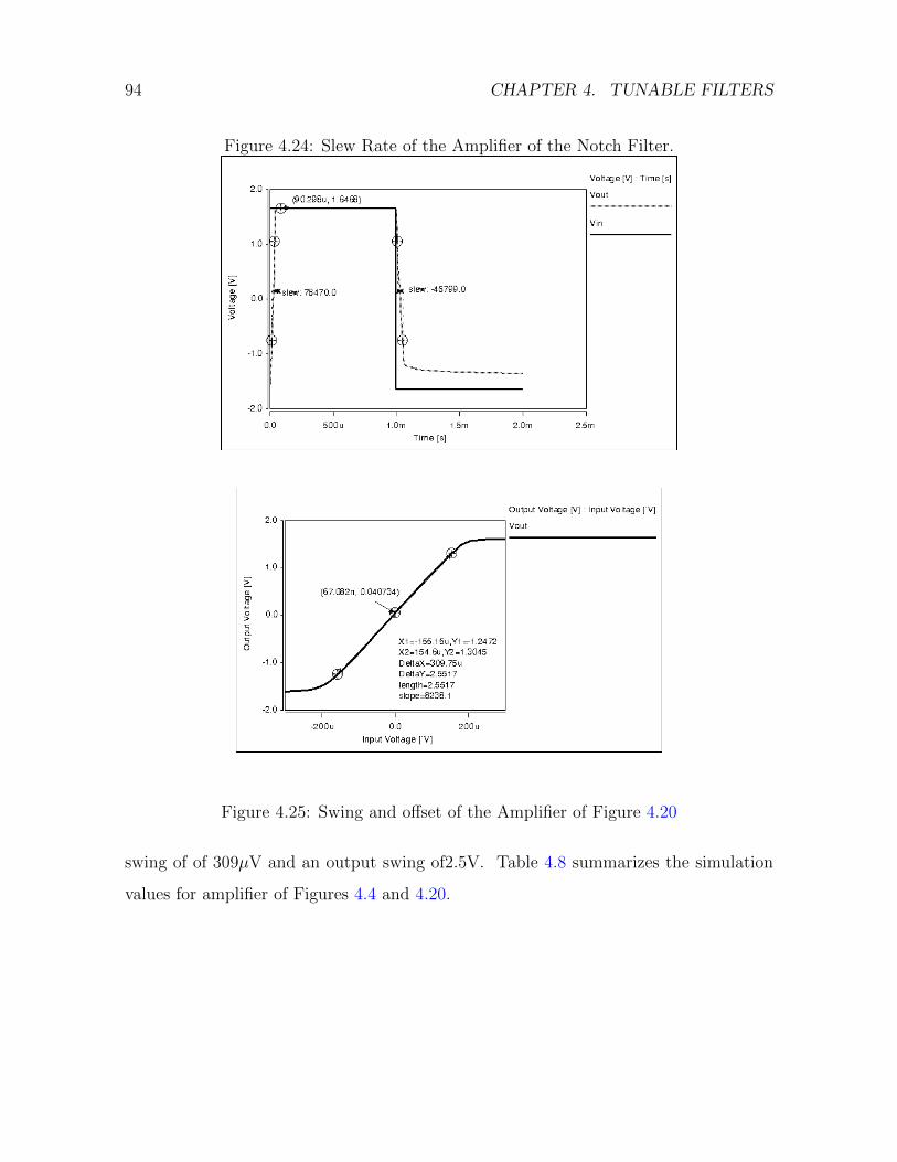
94 CHAPTER 4. TUNABLE FILTERS
Figure 4.24: Slew Rate of the Amplifier of the Notch Filter.
Figure 4.25: Swing and offset of the Amplifier of Figure 4.20
swing of of 309µV and an output swing of2.5V. Table 4.8 summarizes the simulation
values for amplifier of Figures 4.4 and 4.20.

4.3. DESIGN AND SIMULATION RESULTS OF THE TUNABLE NOTCH FILTER95
Table 4.8: Performance Characteristics of the Notch Amplifiers
Block Notch Amplifier
Process Specification 0.5µm
Supply Voltage ±1.65V
Supply Current 25nA
Open Loop Gain 79.7dB
BW 11.59Hz
GBW 95KHz
CMRR @100Hz 91.7dB
PSRR+ @100Hz 84.2dB
PSRR-@100Hz 83.8dB
PM 62.3deg
Output Resistance 29.6MΩ
Systematic Offset 40mV
ICMR 309µV
Output Swing 2.5V
THD(@100mV), ACL=1 @100Hz (0.00041)%
Dynamic Range 45.5dB
SR+/- 78.4mV/µs/45mV/µs
Settling Time 90µs
Pdiss 330nW
CL 10pF
Layout Area 70µm×76µm
Input Refered Noise 530µVRMS
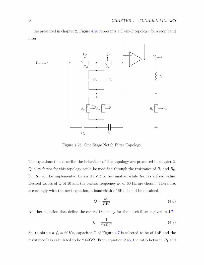
96 CHAPTER 4. TUNABLE FILTERS
As presented in chapter 2, Figure 4.26 represents a Twin-T topology for a stop band
filter.
−
+VinNotch
VoNotch
Rx
Cn Cn
CnCn
VcqRg
VcfRg1
VcfRg1
Vcf
Rg1
Vcf
Rg1
Figure 4.26: One Stage Notch Filter Topology.
The equations that describe the behaviour of this topology are presented in chapter 2.
Quality factor for this topology could be modified through the resistance of R1 and R2.
So, R1 will be implemented by an HTVR to be tunable, while R2 has a fixed value.
Desired values of Q of 10 and the central frequency ωc of 60 Hz are chosen. Therefore,
accordingly with the next equation, a bandwidth of 6Hz should be obtained.
Q =ωcBW
(4.6)
Another equation that define the central frequency for the notch filter is given in 4.7.
fc =1
2πRC(4.7)
So, to obtain a fc = 60Hz, capacitor C of Figure 4.7 is selected to be of 1pF and the
resistance R is calculated to be 2.65GΩ. From equation 2.45, the ratio between R1 and

4.3. DESIGN AND SIMULATION RESULTS OF THE TUNABLE NOTCH FILTER97
R2 for a Q equals to 10 is:
R1 = 39R2 (4.8)
The resistance of R2 is proposed to be 50kΩ and R1 must be 1.95MΩ. Both R1 and R2
will be implemented using HVTR circuits.
To obtain a further attenuation in the frequency rejection band (60Hz), two notch
filters has been cascaded. The block diagram of the cascade implementation of the
band pass filter and notch filter is depicted in Figure 4.27.
Vinn
Vinp
BPF BPF BPF
NOTCH NOTCH Voutp
NOTCH NOTCH Voutp
Figure 4.27: Block diagram of the Tunable Band Pass Filter and Notch
Tunable Notch Filter performance is next presented. Figure 4.28 shows the Notch fre-
quency response and then, Figure 4.29 depicts a central frequency sweep of the Notch
Filter, achieved by variations of Vcf . Then Table 4.9 summarizes the notch performance
parameters.
Table 4.9: Performance parameters of the notch filter obtained by simulation.
fc BW Q IRN(0.05Hz-100Hz) THD(@100Hz) CL
60Hz 21Hz 2.85 3.24mVrms 0.76 % 10pF
Table 4.10 lists the control voltages of the HVTR for each Biomedical Band with central
notch frequency at 60Hz.

98 CHAPTER 4. TUNABLE FILTERS
Figure 4.28: Frequency Response of the Tunable Notch Filter
The layout realization of the notch filter is presented in Figure 4.30.
Figure 4.29: Central Frequency Sweep of the Tunnable Notch Filter
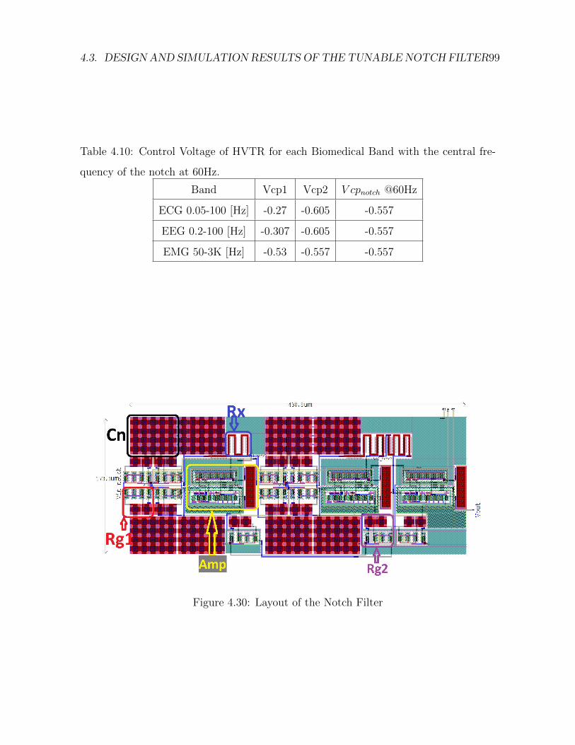
4.3. DESIGN AND SIMULATION RESULTS OF THE TUNABLE NOTCH FILTER99
Table 4.10: Control Voltage of HVTR for each Biomedical Band with the central fre-
quency of the notch at 60Hz.
Band Vcp1 Vcp2 V cpnotch @60Hz
ECG 0.05-100 [Hz] -0.27 -0.605 -0.557
EEG 0.2-100 [Hz] -0.307 -0.605 -0.557
EMG 50-3K [Hz] -0.53 -0.557 -0.557
Figure 4.30: Layout of the Notch Filter

100 CHAPTER 4. TUNABLE FILTERS

Chapter 5
Conclusions
These thesis proposed the design of a Front-End amplifier for biomedical applications,
followed by a band pass filter with tunable bandwidth, which must be able to oper-
ate in the three different bands of interest (ECG, EEG and EMG) and a Notch filter
to perform the line interference filtering. In order to achieve some Figures of Merit
improvements, some design techniques were incorporated to achieve the following per-
formance as presenter in table 5.1.
As presented in Table 5.1 the requirements secifications are: supply voltage is ±
1.65V, the bias curent is <12µA, and CMRR > 120dB.
Table 5.1: Performance of the AmplifierParametro Valor Especificado Valor Obtenido
Alimentacion ±1.65V ±1.65V
Corriente de Polarizacion < 12µA 11.6µA
Ganancia 40dB 40dB
THD < 1% <0.2%
CMRR >120dB Media = 162db
PSRR >60dB 55dB
Offset Entrada/Salida 0.5mV/±50mV
IRN <2µVRMS(0.5Hz − 100Hz) 1.6µVRMS(0.5− 100Hz)
101
102 CHAPTER 5. CONCLUSIONS
Different techniques were implemented in order to achieve the design specifications
of the circuit. Three different combinations of these techniques were simulated. The
first one include an offset compensation scheme of the circuit, the second one a CMRR
enhancement circuit and the third one a combination of CMRR enhancement and offset
compensation scheme.
The best circuit performance was obtained by the first implemented technique, using
dc-feedback to achieve offset compensation of the system, which lead to relax the de-
sign specification of the complementary amplifier of the offset compensation schemme,
which does not need to be offset compensated in DC-servoloop technique, avoiding the
use of Chopper or Auto.Zero techniques and their drawbacks. Moreover, this proposal
allows the reuse of system blocks such as input capacitors of QFG transistors in or-
der to implement the capacitive feedback loop and the reference resistor of the QFG
transistors to reinsert in the system the DC level to compensate the offset. With these
techniques the montecarlo CMRR values range from 152.9dB to 195dB with a mean of
162dB, upgrading the scattered values presenter in [36]. Since the inverte circuit does
not depend on transistors mismatch, given that it depends on the implemented resistive
feedbac, and at the same time, mismatch of two resistive elements is smaller than the
one of active elements, and it can be improved with layout techniques. On the other
hand, the Input Referred Noise achieved was 1.62 µVrms.
The Band Pass Filter tunability is successfully achieved in a wide band of low fre-
quencies (from 0.05Hz to 3kHz) with the use of HVTR elements by means of their
bias voltage with a selectivity step of 10mV. The resistance of High Value Tunable
Resistors could be varied from some Mega Ohms to hundreds of Giga Ohms. With the
notch filter topology, the central frequency can be externally selectable throughout the
HVTR bias. Also, Quality Factor of this filter can be modified with HVTR elements.
Mismatch effects have not been considered in the case of filters due to HVTR tunability
103
allows to deal with such effects. Furthermore, reached resistance values using HVTR
let the use of on-chip capacitors.
As future work, the sensitivity of the HVTR elements should be studied, as well as
temperature variations of the circuit, in order to know the effect of this parameter in
each circuit element. Besides, there must be added to these topologies a technique that
lead to erase and reset the initial value of the QFG transistors.

104 CHAPTER 5. CONCLUSIONS

Bibliography
[1] W. Dabrowski, P. Grybos and A.M. Litke: ”A low noise multichannel integrated
circuit for recording neuronal sinals using microelectrode arrays” Biosensors and
Bioelectronics 10 (2004) 749-761.
[2] Jiawei Xu, Yazicioglu R.F., Harpe, P., Makinwa, K.A.A., Van Hoof, C.: ”A
160µW 8-channel active electrode system for EEG monitoring,” Solid-State Cir-
cuits Conference Digest of Technical Papers (ISSCC), 2011 IEEE International.
[3] Northrop Robert B. ”Analysis and Application of Analog Electronic Circuits
to Biomedical Instrumentation”CRC PRESS, Boca Raton London, New York,
Washington, D.C., 2004 ISBN 0-8493-2143-3
[4] Solıs Bustos Sergio, ”High Performance CMOS Analog Interfaces for Biomedical
Signals Acquisition Systems By High Performance CMOS Analog Interfaces for
Biomedical Signals Acquisition Systems,” PhD Thesis at Instituto Nacional de
Astrofısica, Optica y Electronica, 2001.
[5] Razavi Behzad: ”Design of Analog CMOS Integrated Circuits,” McGRAW-HILL,
Electrical Engineering Series.
[6] Baker, Jacob: ”CMOS: Circuit Design, Layout, and Simulation, 3rd Edition,”
c©2010, Wiley-IEEE Press.
[7] C. D. Motchenbacher, J. A. Connelly: ”Low-Noise Electronic System Design,”
Wiley and Sons, 1993.
105

106 BIBLIOGRAPHY
[8] Pelgrom, Marcel J M, Duinmaijer, Aad C J, Welbers, Anton P G: ”Matching
Properties of MOS Transistors,” IEEE Journal of Solid-State Circuits, vol. 24,
no. 5, october 1989.
[9] Witte Johan F., Makinwa Kofi A., Huijsing Johan H.: ”Dynamic Offset Compen-
sated CMOS Amplifiers,” Springer 2009.
[10] Bakker, Anton, Thiele, Kevin, Huijsing, Johan H: ”A CMOS nested-chopper in-
strumentation amplifier with 100-nV offset,” IEEE International Solid-State Cir-
cuits Conference. Digest of Technical Papers (Cat. No.00CH37056) (2000).
[11] Seo, Inchang, Fox, Robert M.: ”Comparison of quasi-/pseudo-floating gate tech-
niques and low-voltage applications,” Analog Integrated Circuits and Signal Pro-
cessing, vol. 47, 2006.
[12] C. Enz Christian, C. Temes Gabor: ”Circuit Techniques for Reducing the Ef-
fects of Op-Amp Imperfections: Autozeroing, Correlated Double Sampling, and
Chopper Stabilization.” Proceedings of IEEE, vol. 84, November 1996.
[13] Srinivasan, Venkatesh, Serrano Guillermo J., Gray Jordan, Hasler Paul: ”A preci-
sion CMOS amplifier using floating-gate transistors for offset cancellation,” IEEE
Journal of Solid-State Circuits, vol. 42, 2007.
[14] S. Sakunia, F. Witte, M. Pertijs and K. Makinwa: ”A Ping-Pang Current-
Feedback Instrumentation Amplifier with 0.04 % Gain Error”, Symposium on
VLSI Circuits Digest of Technical Papers , 2011.
[15] J. Witte, K. Makinwa and J.Huijsing: ”A CMOS Chopper Offset-Stabilized
Opamp” IEEE Journal of Solid-State Circuits, Vol.42, No. 7, July 2007.
[16] D. Hang and Y. Zheng: ”A Chopper Stabilized Instrumentation Amplifier with
Dual DC Cancellation Servo Loops for Biomedical Applications” IEEE Asian
Solid-State Circuits Conference, November 12-14, 2012, Kobe, Japan.

BIBLIOGRAPHY 107
[17] Harrison Reid R., Charles Cameron: ”A low-power low-noise CMOS amplifier for
neural recording applications,” IEEE Journal of Solid-State Circuits, 2003.
[18] M. Yin and M. Ghovanloo: ”A Flexible Clockless 32-ch Simultaneous Wireless
Neural Recording System with Adjustable Resolution,” ISSCC 2009 Dig Tech Pa-
pers, pp. 432-433, Feb. 2009.
[19] Thanigaivelan, Balavelan, Wiles, Janet, Hamilton, Tara Julia: ”A low power
neural recording amplifier with programmable gain and bandwidth,” ISCAS 2012
- 2012 IEEE International Symposium on Circuits and Systems.
[20] Yazicioglu, Refet Firat, Merken, Patrick, Puers, Robert, Van Hoof, Chris: ”A
60 uW 60 nV/sqrt(Hz) Readout Front-End for Portable Biopotential Acquisition
Systems,” IEEE Journal of Solid-State Circuits, vol. 42, issue 5, pgs. 1100-1110,
2007.
[21] Castro, Pablo, Silveira, Fernando: ”High CMRR power efficient neural recording
amplifier architecture,” Proceedings - IEEE International Symposium on Circuits
and Systems, 2011.
[22] Chon-Teng Ma, Pui-In Mak, Mang-I Vai, Peng-Un Mak, Sio-Hang Pun, Wan
Feng, Martins, R.P: ”A 90nm CMOS bio-potential signal readout front-end with
improved powerline interference rejection,” Circuits and Systems, 2009. ISCAS
2009. IEEE International Symposium.
[23] Haiyan Zhou, Matthias Voelker, Johann Hauer: ”A Mixed-Signal Front-End ASIC
for EEG Acquisition System,” IEEE 2012.
[24] Qiang, Li, Kuo, Hwi Roy Tan, Teo, Tee Hui, Singh, Rajinder: ”A 1-V 36-µW
low-noise adaptive interface IC for portable biomedical applications,” ESSCIRC
2007 - Proceedings of the 33rd European Solid-State Circuits Conference.
108 BIBLIOGRAPHY
[25] Wen-Sin Liew, Xiaodan Zou, Libin Yao, Yong Lian: ”A 1-V 60µW 16-Channel
Interface Chip for Implantable Neural Recording,” IEEE Custom Integrated Cir-
cuits Conference, 2009.
[26] Wu, Honglei, Xu, Yong Ping: ”A 1V 2.3µW Biomedical Signal Acquisition IC,”
IEEE International Solid-State Circuits Conference, 2006.
[27] Zou, Xiaodan, Xu, Xiaoyuan, Yao, Libin, Lian, Yong: ”A 1-V 450-nW fully
integrated programmable biomedical sensor interface chip,” IEEE Journal of Solid-
State Circuits, vol. 44, issue 4, pgs. 1067-1077, 2009.
[28] Li, Haixi, Zhang, Jinyong, Wang, Lei: ”A fully integrated continuous-time 50-Hz
notch filter with center frequency tunability,” Proceedings of the Annual Inter-
national Conference of the IEEE Engineering in Medicine and Biology Society,
EMBS, 2011.
[29] Ling Chaodong, Ye Pizhou, Liu Rong, Wang Jiaxian: ”A Low-pass Power Notch
Filter Based on An OTAoC Structure for Electroencephalogram,” Proceedings of
2007, International Symposium of Intelligent Signal Processing and Communca-
tion Systems, Nov. 2008.
[30] C.-T. Ma, P.-I. Mak, M.-I. Vai, P.-U. Mak, S.-H. Pun, W. Feng and R.P. Martins:
”Frequency-bandwidth-tunable powerline notch filter for biopotential acquisition
systems”, Electronic Letters, vol. 45 no. 4, 12th February 2009.
[31] Baschirotto A, Bijno D., Castello, R., Montecchi, F.: ”A 1 V 1.2 µW 4th order
bandpass switched-opamp SC filter for a cardiac pacer sensing stage,” Circuits and
Systems, 2000. Proceedings. ISCAS 2000 Geneva. The 2000 IEEE International
Symposium on (Volume 3).
[32] Salthouse Christopher D, Sarpeshkar, R.: ”A practical micropower programmable
bandpass filter for use in bionic ears,” Solid-State Circuits, IEEE Journal of (Vol-
ume:38 , Issue: 1).
BIBLIOGRAPHY 109
[33] H. Elhallabi, M. Sawan: ”High Frequency and High Q CMOS Gm-C Bandpass
Filter with Automatic On-chip Tuning,” The 13th International Conference on
Microelectronics, Rabat, Morocco, Oct. 2001.
[34] Yang, M., Liu, J., Xiao, Y., Liao, H.: ”14.4 nW fourth-order bandpass filter for
biomedical applications,” Electronic Letters, 2010, Vol. 46.
[35] Pelgrom, M.J.M., Tuinhout, H.P., Vertregt, M.: ”Transistor matching in ana-
log CMOS applications,”International Electron Devices Meeting 1998. Technical
Digest (Cat. No.98CH36217).
[36] Safari, Leila, Azhari, Seyed Javad: ”An ultra low power, low voltage tailless QFG
based differential amplifier with High CMRR, rail to rail operation and enhanced
slew rate,” Analog Integrated Circuits and Signal Processing, vol. 67, pgs. 241-
252, 2011.
[37] :Christian C. Enz, Gabor C. Temes ”Circuir Techniques for reducing the Effects of
Op-Amp Imperfections: Autozeroing, Correlated Double Sampling, and Chopper
Stabilization” Proceedings of the IEEE Vol.84, No. 11, November 1996.
[38] Muniz, C., Diaz, A., Carvajal, R.G.: ”Offset compensation using unbalanced po-
larization,” 2006 IEEE International Symposium on Circuits and Systems.
[39] Gabriel Vasilescu: ”Electronic Noise and Interfering Signals: Principles and Ap-
plications,” Springer Science and Business Media, Jan 12, 2005.
[40] Cherem Schneider Marcio, Galup-Montoro Carlos: ”CMOS Analog Design Using
All-Region MOSFET Modeling,” Cambridge University Press, 2010.
[41] Paul Jespers: ”The Gm-ID Methodology, A Sizing Tool for Low-Voltage Analog
CMOS Circuits,” @Springer Science+Business Media, LLC 2010.
[42] Muniz-Montero Carlos: ”Nuevas estrategias para compensacion de offset en blo-
ques de diseno analogico,” PhD Thesis at INAOE, 2008.

110 BIBLIOGRAPHY
[43] Esther Rodriguez-Villegas: ”Low Power and Low Voltage Circuit Design with the
FGMOS Transistor,” The Institution of Engineering and Technology, London,
2006.
[44] Phillip E. Allen, Douglas R. Holberg: ”CMOS Analog Circuit Design,” Oxford
University Press, 2002.
[45] David M. Binkley: ”Tradeoffs and Optimization in Analog CMOS Design,” John
Wiley and Sons, Ltd., Publication.
[46] Jim Hellums, Ph.D.: ”Noise Analysis for CMOS Amplifiers,” Class notes, the
University of Texas at Dallas.
[47] Vittoz, E.a.: ”The Design of High-Performance Analog Circuits on Digital CMOS
Chips,” IEEE Journal of Solid-State Circuits, vol. 20, issue: 3, pgs. 657-665, 1985.
[48] Steve Winder: ”Analog and Digital Filter Design, Second Edition,” DN Series for
Design Engineers, 2002.
[49] A. Tajalli, Y. Leblebici and E.J. Brauer: ”Implementing ultra-high value floating
tunable CMOS resistors,” Electronic Letters, 2008, Vol. 44.
[50] Bikumandla Manoj, RamIrez-Angulo Jaime, Urquidi Carlos Carvajal, Ramon G.
Lopez-Martin, Antonio J.: ”Biasing CMOS amplifiers using MOS transistors in
subthreshold region,” IEICE Electronics Express, 2004, Vol. 1. No. 12, pgs. 339-
345
[51] Palmisano G., Palumbo G., Pennisi S.: ”Design Procedure for Two-Stage CMOS
Transconductance Operational Amplifier: A Tutorial,” Analog Integrated Circuits
and Signal Processing, 2001.