Embed Size (px)
DESCRIPTION
A High dI/dt CMOS Differential Optical Transmitter for a Laser Diode. HSSPG. Doctoral Dissertation Presentation by Sungyong Jung. Advisor: Martin A. Brooke. School of Electrical and Computer Engineering Georgia Institute of Technology, Atlanta, GA, 30332 March 28, 2002. Outline. HSSPG. - PowerPoint PPT Presentation
Citation preview

1HSSPG
Doctoral Dissertation Presentation
by
Sungyong Jung
Advisor: Martin A. Brooke
School of Electrical and Computer Engineering
Georgia Institute of Technology, Atlanta, GA, 30332
March 28, 2002
A High dI/dt CMOS Differential Optical Transmitter for a Laser Diode

2
Introduction
Background
Application
A Differential laser driver
Packaging Parasitic Consideration
Test Results
A Driver for LVDS Standard
Conclusion and Future Work
HSSPG
Outline

3
Introduction
Why Optical Interconnection?Larger bandwidth than conventional interconnects
Low power consumption
Low parasitics
Smaller channel crosstalk
Shorter interconnection delays
Why CMOS?Low power
High yield
Low cost
Higher degree of integration
HSSPG

4
Introduction
Objective
Development of drivers for optical interconnect
Using Available Standard Digital CMOS Technology
Predicting the behavior including parasitic models
Working at commercially interesting high speed with high
output current
HSSPG

5
BackgroundOptical interconnection system
HSSPG
RecoveredInformation
InformationSource
OpticalTransmitter
OpticalReceiver
OpticalSource
OpticalMedia
OpticalDetector

6
BackgroundEye Diagram
HSSPG
Logic "1" level
1 + Y1
1
1 - Y1
0.5
Y1
0
- Y1
0 X1 X2 1 - X2 1 - X1 1
Logic "0" level
Time [UI]
Nor
mal
ized
Am
plitu
de
Rates X1 X2 Y1
OC-1 and OC-3
0.15 0.35 0.20
OC-9 through OC-24
0.25 0.40 0.20
Visual method to measure the
properties of a data stream
A composite of multiple puslses captured with
a series of triggers based on the data-clock pulse
Jitter: close in the horizontal direction due to the
variations in the pulse duration or the accuracy
of the pulse stream’s clock
ISI, Noise: close in vertical direction

7
BackgroundOptical Sources
HSSPG
LED – Low speed communication
Simpler fabrication
Lower cost
High reliability
Less temperature dependence
Simpler driver circuitry
Higher linearity
LASER – High speed communication
High output power
Lower divergence degreeCurrent
LightOutput(Power)
Threshold current
Laser
LED
The light output versus current characteristic of laser and LED.

8
BackgroundOptical Drivers
HSSPG
LED
Vin
VCC
VEE
R1
R2
Laser
VSSVbias
InputSignal Rmod
An example of the laser driver An example of the LED driver circuit

9
Application2 & 3 Layer Thru-Silicon Optical Interconnect System
High bandwidth
Low loss
Small crosstalk
Short interconnect delay
Massively parallel interconnection
HSSPG

10
ApplicationBasic Structure of Thru-Silicon Interconnect
Emitter DriverSilicon Circuitry
InGaAsPEmitter
Detector AmplifierSilicon Circuitry
InP/InGaAsPDetector
Emitter DriverSilicon Circuitry
InGaAsPEmitter
Detector AmplifierSilicon Circuitry
InP/InGaAsPDetector
HSSPG

11
Separate fabrication
high yield
indep. Optimize
Reduce the packaging parasiticsFinal Integration
Integration of hybrid thin-film device
HSSPG
2 & 3 Layer Optical Link

12
Application
HSSPG
I-MSM photodetector
Larger area with lower
capacitance than PiN detector
Metal fingers on the bottom
0.7 A/W Responsivity
250µm size: alignment tolerant
1.1 GHz operation in this size
Resonant Cavity LED
Improved spectral purity
100µm square device
Long wavelength (.3m)
100 Mbps operation in this
size
13
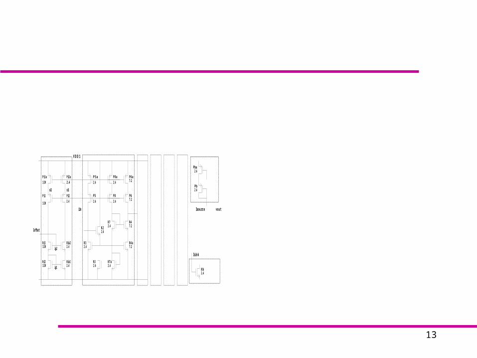
N2
N3
N1
N7a
N7 N4
N4a
Nb
P5 P8 P6
P6aP8aP5aPi2a
Pi2Pi1
Pi1a
Pba
Pb
Nia2
Nia1
Ni1
Ni2
2.4
2.4
2.4
2.4
2.4 2.4
2.4
2.4
2.4
7.2
7.2
7.2
7.22.4
2.4
2.4
2.4120
120
2.4
120
120
2.4
2.4
voutiin
Isink
Ioffset
Isource
VDD1
ig2
ig1
si1si2
VDD2
VSS1 VSS2
Stage 1Offset
BiasP
BiasN
R L
AI = 3 AI = 3 AI = 3 AI = 3 AI = 3
Receiver Single-ended
0.8 um Si CMOS technology
Application
HSSPG

14HSSPG
Application
Eye diagram for 50um MSM Pulse diagram for 50um MSM
2 ns/div 19.04 ns-960 ps
-6.5 mV
5mV/div
13.5 mV
50 ns/div 256 ns-244 ns
-3.5 V
500mV/div
1.5 V
Test Results of Integrated Receiver at 155 Mbps

15
LED DriverSingle-ended
0.8 um CMOS technology
Application
HSSPG
M1
M2
M3
M7
M5
M6
M9 M10 M11 M12
M4
M8
D1
I2
I1
V1
VDD
VSS

16
Application
HSSPG
Test Results of Integrated Transmitter at 155 Mbps
250um & 100 um InGaAlAs integrated TX

17
Application
HSSPG
Test setup144 pin PGA package
Test setup block diagramTest board with a bonded chip
Clock for Transient output curve and BER synchronization
Microwave Logic
giga BERT-1400 TXLED Driver
Microwave Logic
giga BERT-1400 RX
Tektronix 11403AOscilloscope
Receiver

18
Test result of 2-layer interconnection
PRBS 27-1 at 40 Mbps, 1x10⁻⁹ BER
2-layer diagram 40 Mbps RX output
Application
HSSPG

19
3-layer link
3-layer stacked chip
HSSPG
Application
The measured eye diagram of three-layer system at 1 Mbps
20
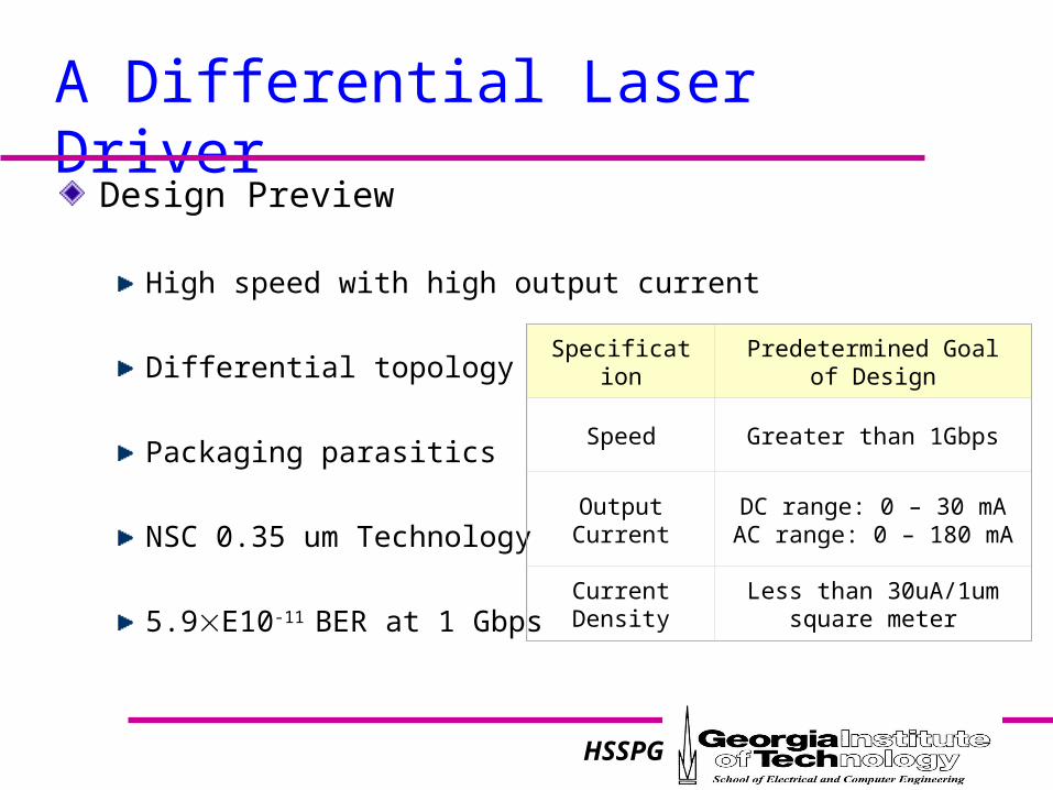
A Differential Laser Driver
HSSPG
Design Preview
High speed with high output current
Differential topology
Packaging parasitics
NSC 0.35 um Technology
5.9E10-11 BER at 1 Gbps
SpecificationPredetermined Goal of
Design
Speed Greater than 1Gbps
Output CurrentDC range: 0 – 30 mA
AC range: 0 – 180 mA
Current DensityLess than 30uA/1um square
meter

21
A Differential Laser Driver
HSSPG
Lb: Induction due to wire bond
Cp: Capacitance of the laser chip
Rs: Metal contacts
Rj: Resistance from p-n junction
Cj: Capacitance from p-n junction
Lb Rs
Rj CjCp
Model of a Laser

22
A Differential Laser Driver
Simulation result at 1 Gbps
HSSPG
• 180 mA peak-to-peak modulation current• 30 mA laser biasing current• 0.35 um Si CMOS technology
Circuit Schematic
D2
M1 M2
M5
M6
M7M3M4
ImodIth
V2V1
VDD
VSS
Z1

23
A Differential Laser Driver
HSSPG
Simulation Results
Temperature simulation at 27 and 200
•Top: Pulse output at 27•Second: Eye diagram at 27•Third: Pulse output at 200•Bottom: eye diagram at 200
Transient response at 2 Gbps •Top: Input pulse •Middle: Pulse output •Bottom: eye diagram

24
A Differential Laser Driver
HSSPG
Scalability0.18 um technology
Transient response at 10 Gbps •Top: Input pulse •Middle: Pulse output •Bottom: eye diagram
MAGIC layout •Scale factor: 1.944•Bandwidth: gm/C

25
Packaging Parasitics
HSSPG
Background – delta-I noise
VpC_decouple
L_parasitics
Vin
Vc
dt
dILVc
Degrade the edge rate
Reduce noise margins
Cause false switching

26
Packaging Parasitics
HSSPG
Printed Circuit Board Design
l 2l 1 l 3 l 4 l 5
w 2w 1 w 3
PCB for TX testing Metal line in PCB
27
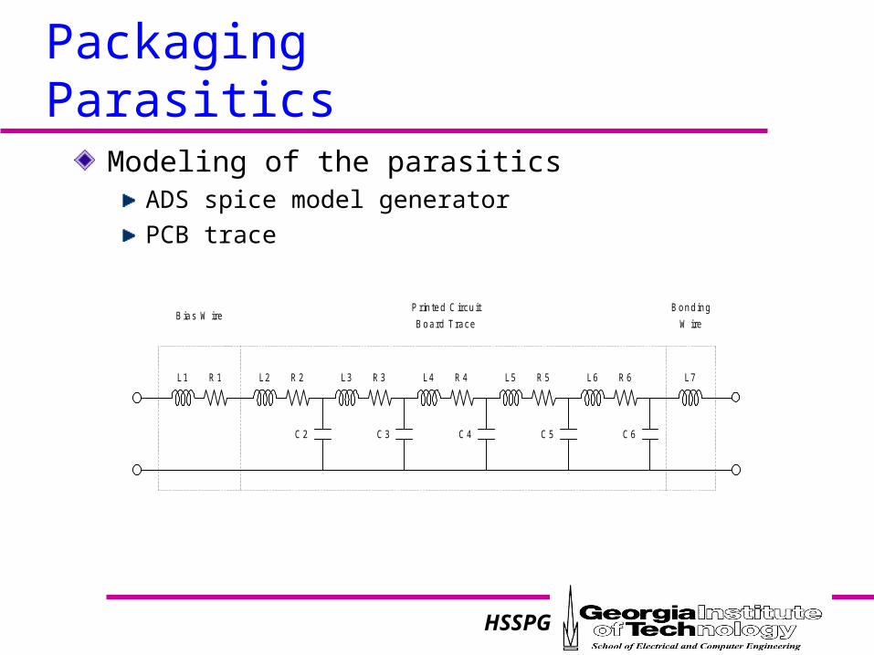
Packaging Parasitics
HSSPG
Modeling of the parasiticsADS spice model generator
PCB trace
L3 R 3
C 3
L2 R 2
C 2
L4 R 4
C 4
L5 R 5
C 5
L6 R 6
C 6
L7L1 R 1
B ias W ireP rin ted C ircu it
B oard T race
B ond ing
W ire

28
Packaging Parasitics
HSSPG
Modeling of the parasiticsInductance of Bonding wires
)1)4
(ln(2
r
o
d
llL
o: the permeability of free space,
r: the relative permeability of
the bonding wire material, d: the diameter of the boding wire, l: is the length of the bonding wire, : the skin effect factor
)4
tanh(25.0d
ds
ds is: the skin depth of the bonding wire
material
0
rs
fd
: the resistivity of the bonding wire material f: the frequency

29
Packaging Parasitics
HSSPG
The value of parasitics
Parameter Value Parameter Value
L1 105 nH C4 0.367874 pF
L2 1.38664 nH C5 0.367874 pF
L3 1.38664 nH C6 0.367874 pF
L4 1.38664 nH R1 0.1
L5 1.38664 nH R2 0.0280365
L6 1.38664 nH R3 0.0280365
L7 3.996 nH R4 0.0280635
C2 0.367874 pF R5 0.0280635
C3 0.367874 pF R6 0.0280635

30
Packaging Parasitics
HSSPG
Solutions for reducing delta-I noise
Differential topology- Eliminate noise by using symmetric but inverse current flowing path
to the power supply lines.
Decoupling Capacitor- Maintain the constant dc power supply levels.
,dt
dVCI
C
I
dt
dV

31
Packaging Parasitics
HSSPG
Bias Stablization Simulation
Single-Ended Version Bias Current (Has a Signal Component)
Differential Version Bias Current (No Signal Component)

32
Packaging Parasitics
HSSPG
The model of decoupling capacitors
ESR: Equivalent series resistance
ESL: Equivalent series inductance
ESR
ESL
C

33
Packaging Parasitics
HSSPG
Parasitic effect simulation
Simulation result with parasitic model• No open eyes
Simulation result with ideal decoupling capacitor
1 nF Decoupling capacitance
10 nF Decoupling capacitance

34
Packaging Parasitics
HSSPG
Simulation with real model
Simulation result with real decoupling capacitor model
ESR: 0.855 Ohm
ESL: 1.12 nH
C: 10.015 nF

35
Packaging Parasitics
HSSPG
Chip layout and farbrication
The driver
Decoupling capacitor
Decoupling capacitor The driver circuit•Layout in Cadence•Minimized depletion capacitance•NSC 0.35 um technology

36
Test Results
HSSPG
Test setupChip-on-Board (COB) technology
Test setup block diagramTest board with a bonded chip
Clock for Transient output curve and BER synchronization
Microwave Logic
giga BERT-1400 TXLaser Driver
Microwave Logic
giga BERT-1400 RX
Tektronix 11403AOscilloscope

37
Test Results
HSSPG
Transient response test
•0.1 uF decoupling capacitor•27-1 NRZ PRBS•200 Mbps operation

38
Test Results
HSSPG
Transient response test @ 622 Mbps
•10 nF decoupling capacitor•27-1 NRZ PRBS•10-11 BER

39
Test Results
HSSPG
Transient response test @ 900 Mbps
•10 nF decoupling capacitor•27-1 NRZ PRBS•0.210-11 BER
40
Test Results
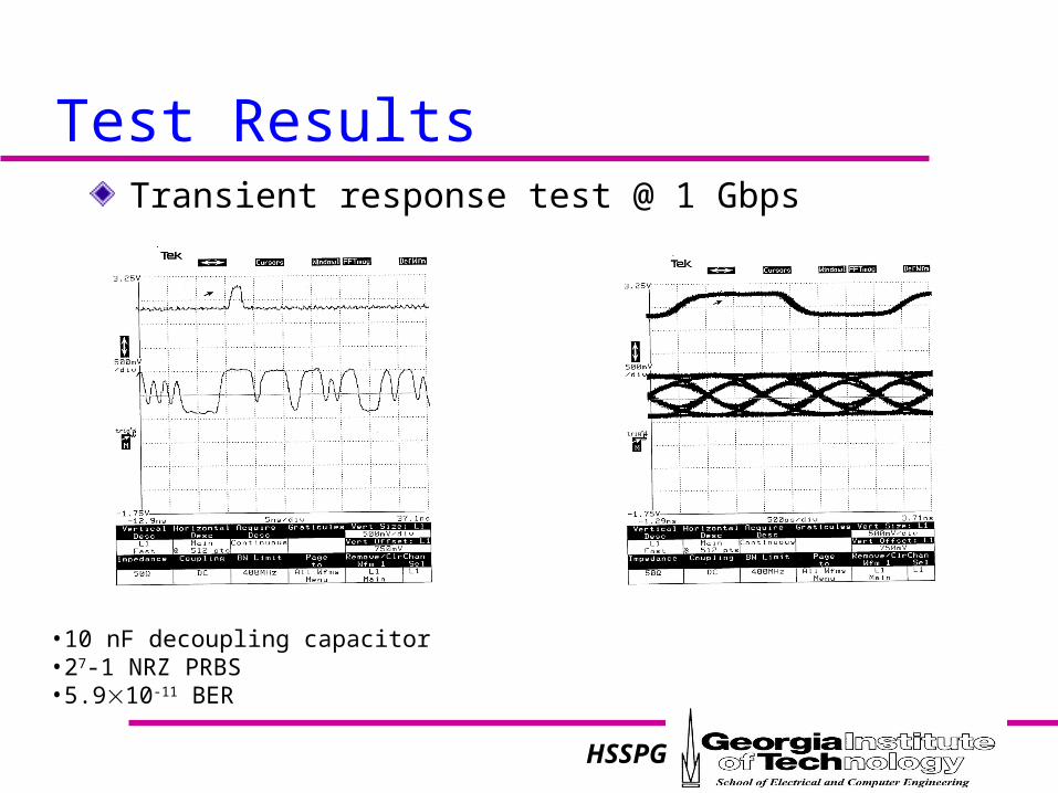
HSSPG
Transient response test @ 1 Gbps
•10 nF decoupling capacitor•27-1 NRZ PRBS•5.910-11 BER

41
Test Results
HSSPG
Analysis with additional parasitics
Simulation results at 1 Gbps •Top: Input pulse •Middle: Pulse output •Bottom: eye diagram

42
A Driver for LVDS StandardObjectives
Design a laser driver compatible with LVDS IEEE standard
HSSPG
Specification Predetermined Goal of Design
Speed Up to 1Gbps
Input magnitude > 400 mV
Power supply 2.5 V
Output currentDC range: 0 – 30 mAAC range: 0 – 40 mA
Current density Less than 30uA/1um square meter

43
Pre-driver circuit design
A Driver for LVDS Standard
HSSPG
V1
VDD
VSS
M9
M7 M3 M4 M8
M1 M2
M5M6
V2
I1
I2 Out-
Out+
Dmoxn
Dmoxn
m
mv
ILWC
ILWC
g
gA
3
1
3
1
)/(2
)/(2

44
Overall circuit schematic
Circuit diagram Simulation result at 1 Gbps
A Driver for LVDS Standard
HSSPG
V1
M 18
M 16 M 12 M 13 M 17
M 10 M 11
M 14M 15
I3
I4
M 9
M 7 M 3 M 4 M 8
M 1 M 2
M 5M 6
V2
I1
I2
VDD
D2
M 19 M 20
M 24
M 23
M 25M 21M 22
I5 I6
VSS
Z1

45
Chip layout and fabrication
A Driver for LVDS Standard
HSSPG
Receiver
Transmitter
DAC
Decoupling Capacitor
•Layout in MAGIC•TSMC 0.25 um technology

46
Conclusion and Future Work
HSSPG
Ref. ProcessChannel Length[m]
Speed [Gbit/s]
Max. Output Current
[mA]
Eye Diagram
BER Remark
This Wor
kCMOS 0.35 1 180 Yes Yes
-Measure in packaging
-Electrical test
This Wor
kCMOS 0.25 1 40 No No
-Only simulation results
[27] CMOS 0.5 m 2.5 1.6 Yes Yes-On-wafer measure
-Optical test
[28] CMOS 1.2 m 1 1.2 Yes Yes -Optical test
[29] CMOS 1.0 m 0.622 25 Yes No-On-wafer measure
-Optical test
[21] CMOS 0.8 m 1.5 GHz NA No No-On-wafer measure
-Electrical test
[33] CMOS 0.35 m 1 NA No No-Only simulation
results
ComparisonHighest current driving capability at Gbps speed
Not many drivers with BER and/or eye-diagram

47
Conclusion and Future Work
HSSPG
Conclusion
High-speed and high-current optical transmitter were designed,
simulated, fabricated, and tested using CMOS technology
Packaging parasitics was modeled and incorporated in the driver
design
Differential topology was employed
the model of decoupling capacitor was included in the simulation and
proper value was estimated and verified
The driver compatible with LVDS IEEE standard was designed,
simulated, and fabricated

48
Conclusion and Future Work
HSSPG
Future Work
Compatible receiver part for transceiver system
Additional function blocks such as a multiplexer or
a predistorter circuit
Verification of LVDS driver circuitry