Embed Size (px)
Citation preview
1
Jordan Addison and Erin Ibarra 6.111 Final Project Report 12/11/14
Digital Debussy: A Hardware-Based Music Composition Tool Abstract Music composition programs are powerful tools for beginning musicians and experienced professionals; however, most of these programs are expensive and in some cases cost hundreds of dollars. While this may be a worthwhile investment for serious musicians, most amateurs do not require the powerful features and tools of professional music composition software. Our goal is to develop a cost-effective, hardware based music composition platform that is easy to use for musicians of all ages and skill levels. Our secondary goal is to include expansion capability to potentially include additional features time permitting.
The main feature of our project is the music writing and playback system. A user will have the ability to input a melody using a graphical representation of sheet music and toolbar to adjust a variety options, such as note duration; he or she will be able to playback the melody through the Labkit speakers. Our goals were to utilize existing sound files that represent various instruments so the user can customize his or her music further. We also planned to implement a control system for the tempo of the music so a user can speed up or slow down his or her music.
2
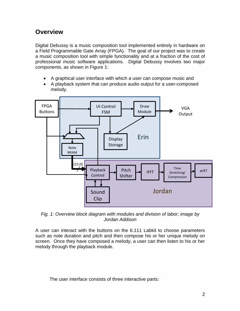
Overview
Digital Debussy is a music composition tool implemented entirely in hardware on a Field Programmable Gate Array (FPGA). The goal of our project was to create a music composition tool with simple functionality and at a fraction of the cost of professional music software applications. Digital Debussy involves two major components, as shown in Figure 1:
A graphical user interface with which a user can compose music and
A playback system that can produce audio output for a user-composed melody.
Fig. 1: Overview block diagram with modules and division of labor; image by Jordan Addison
A user can interact with the buttons on the 6.111 Labkit to choose parameters such as note duration and pitch and then compose his or her unique melody on screen. Once they have composed a melody, a user can then listen to his or her melody through the playback module. The user interface consists of three interactive parts:
FPGA Buttons
UI Control FSM
Sound Clip
FFT
IFFT Playback Control
Time Stretching/
Compression
ac97
Draw Module
Note BRAM
[15:0]
Pitch Shifter
Erin
Jordan
Display Storage
VGA Output
3
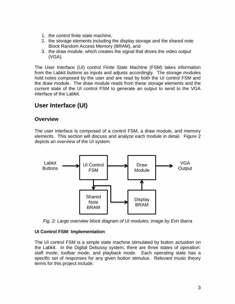
1. the control finite state machine, 2. the storage elements including the display storage and the shared note
Block Random Access Memory (BRAM), and 3. the draw module, which creates the signal that drives the video output
(VGA). The User Interface (UI) control Finite State Machine (FSM) takes information from the Labkit buttons as inputs and adjusts accordingly. The storage modules hold notes composed by the user and are read by both the UI control FSM and the draw module. The draw module reads from these storage elements and the current state of the UI control FSM to generate an output to send to the VGA interface of the Labkit.
User Interface (UI) Overview The user interface is composed of a control FSM, a draw module, and memory elements. This section will discuss and analyze each module in detail. Figure 2 depicts an overview of the UI system.
Fig. 2: Large overview block diagram of UI modules; image by Erin Ibarra UI Control FSM: Implementation The UI control FSM is a simple state machine stimulated by button actuation on the Labkit. In the Digital Debussy system, there are three states of operation: staff mode, toolbar mode, and playback mode. Each operating state has a specific set of responses for any given button stimulus. Relevant music theory terms for this project include:
UI Control FSM
Draw Module
Shared Note
BRAM
Display BRAM
Labkit Buttons
VGA Output
4
1Fig. 4: Layout of buttons; image by Erin Ibarra
Accidental: a modifier that alters the pitch of a note by one semitone on the classical Western scale; a sharp accidental raises a pitch and a flat accidental lowers a pitch.
Attribute: a general feature of a note or of the unique composition.
Attribute Specific: a specific value of an attribute; for example, an attribute specific of pitch would be A.
Beat: the basic unit of musical time, analogous to a letter in a word.
Dot: when a dot is placed next to a note, half of that note’s duration is added to its existing value (a whole note lasting 4 beats with a dot would last 6 beats).
Duration: length of time of a note (whole note, half note, etc.).
Dynamic: the relative loudness or softness in sound of a note.
Measure: a subdivision of a piece of music; refers to a group of notes whose durations sum to a value dictated by the time signature; analogous to a word.
Octave: refers to the specific location of a pitch on the piano; as a reference, middle C on a piano is C4.
Pitch: the letter name assigned to a specific frequency in standard classical Western music (A, B, C, D, E, F, G).
Rest: a duration of silence in a piece of music.
Time Signature: a construct that dictates how many beats are in a given measure of music and the specific note duration equivalent to one beat.
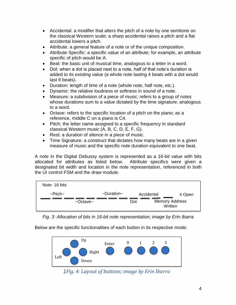
A note in the Digital Debussy system is represented as a 16-bit value with bits allocated for attributes as listed below. Attribute specifics were given a designated bit width and location in the note representation, referenced in both the UI control FSM and the draw module.
Fig. 3: Allocation of bits in 16-bit note representation; image by Erin Ibarra
Below are the specific functionalities of each button in its respective mode:
Note- 16 bits
~Pitch~
~Octave~
~Duration~
Dot
Accidental 4 Open
Memory Address Written
Up
Right
Down Left
Enter 0 1 2 3
5
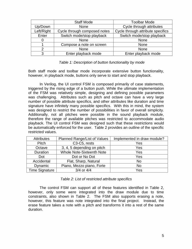
Table 1: Description of button functionality by mode
Both staff mode and toolbar mode incorporate extensive button functionality, however, in playback mode, buttons only serve to start and stop playback. In Verilog, the UI control FSM is composed primarily of case statements, triggered by the rising edge of a button push. While the ultimate implementation of the FSM was relatively simple, designing and defining possible parameters was challenging. Attributes such as pitch and octave can have a very large number of possible attribute specifics, and other attributes like duration and time signature have infinitely many possible specifics. With this in mind, the system was designed to restrict the number of possibilities in favor of overall simplicity. Additionally, not all pitches were possible in the sound playback module, therefore the range of available pitches was restricted to accommodate audio playback. The UI control FSM was designed such that these restrictions would be automatically enforced for the user. Table 2 provides an outline of the specific restricted values.
Table 2: List of restricted attribute specifics
The control FSM can support all of these features identified in Table 2,
however, only some were integrated into the draw module due to time constraints, also shown in Table 2. The FSM also supports erasing a note, however, this feature was note integrated into the final project. Instead, the erase feature takes a note with a pitch and transforms it into a rest of the same duration.
Staff Mode Toolbar Mode
Up/Down None Cycle through attributes
Left/Right Cycle through composed notes Cycle through attribute specifics
Enter Switch mode/stop playback Switch mode/stop playback
0 None None
1 Compose a note on screen None
2 None None
3 Enter playback mode Enter playback mode
Attributes Planned Range/List of Values Implemented in draw module?
Pitch C3-C5, rests Yes
Octave 3, 4, 5 depending on pitch Yes
Duration Whole Note-Sixteenth Note Yes
Dot Dot or No Dot Yes
Accidental Flat, Sharp, Natural No
Dynamic Piano, Mezzo piano, Forte No
Time Signature 3/4 or 4/4 Yes
6
UI Control FSM: Debugging
The UI control FSM was debugged primarily using the ModelSim simulator to analyze signals and ensure proper operation. There were, however, subtle errors in the FSM that were unnoticed until it was integrated into the overall system. The FSM responded to the entire duration of a button push instead of just the rising edge. This resulted in unpredictable state changes and visibly fuzzy transitions of images in the draw module. UI Control FSM: Analysis and Recommendations
Overall, the implementation of the UI control FSM was effective and efficient. The design of the system is simple enough such that more attributes and attribute specifics can be easily integrated into the system. The FSM was designed such that the attribute list and attribute specifics looped once a user reached the end or beginning of a specific list, since the FSM supported movements forward or backward through a list. This looping method is recommended for anyone attempting to create a similar project. Draw Module: Implementation
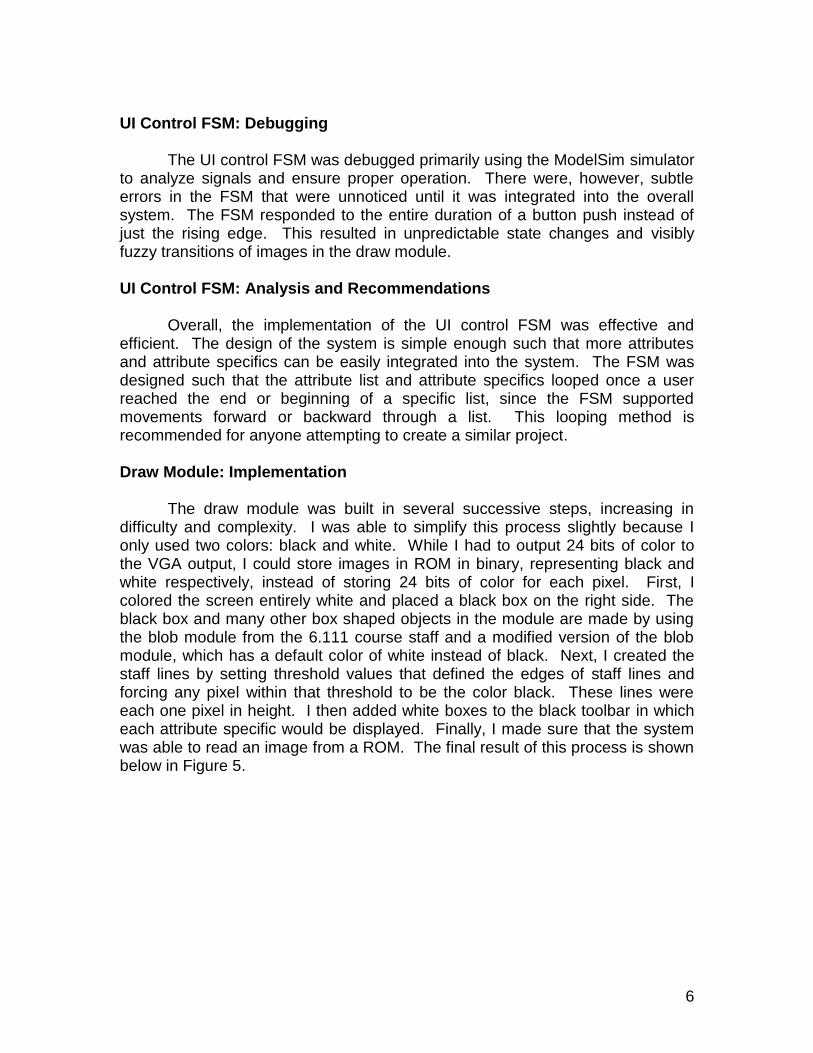
The draw module was built in several successive steps, increasing in difficulty and complexity. I was able to simplify this process slightly because I only used two colors: black and white. While I had to output 24 bits of color to the VGA output, I could store images in ROM in binary, representing black and white respectively, instead of storing 24 bits of color for each pixel. First, I colored the screen entirely white and placed a black box on the right side. The black box and many other box shaped objects in the module are made by using the blob module from the 6.111 course staff and a modified version of the blob module, which has a default color of white instead of black. Next, I created the staff lines by setting threshold values that defined the edges of staff lines and forcing any pixel within that threshold to be the color black. These lines were each one pixel in height. I then added white boxes to the black toolbar in which each attribute specific would be displayed. Finally, I made sure that the system was able to read an image from a ROM. The final result of this process is shown below in Figure 5.
7
Fig. 5: The first trial of graphics display; image by Erin Ibarra
The next step involved displaying the attributes, attribute specifics, and notes on screen. The draw module takes the state of the UI control FSM as an input, so it can display the appropriate attribute specifics in each display box. The attributes themselves are unchanging elements read from ROMs. Each necessary letter was created as 24-bit bitmap file, resized, and transformed into a coefficient file that could be interpreted and loaded into a ROM; the transformation process was completed by a MATLAB script provided by the 6.111 staff. After estimating the appropriate positions for each letter, I used combinational logic to calculate the addresses of each letter and then continuous assignment statements to display the letters on screen. Originally, each letter was black on a white background, so in order to display them as white, I negated the output of the letter ROMs. The treble and bass clef were also created and displayed in this fashion because they were unchanging elements of the graphical user interface.
Similarly, the ROMs containing the attribute specifics were created by
acquiring the image, resizing, and transforming them into a coefficient file. The draw module selected which attribute specific to output to the VGA based on the input information from the state of the UI control FSM through combinational logic.
I found developing the note display portion of the draw module to be the
most complex and challenging part of the project. When a user transcribed a note, the note’s 16-bit representation was stored in the shared BRAM and in the display BRAM. The draw module read from the note BRAM every clock cycle
8
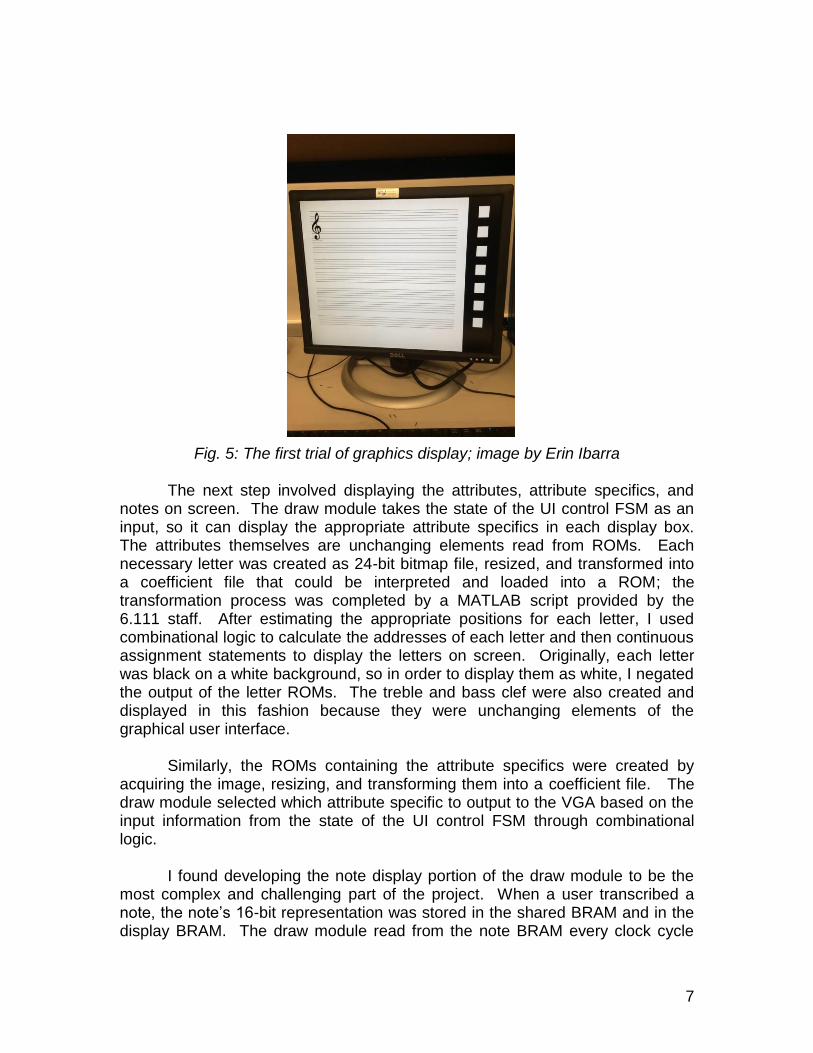
and collected information on each note sequentially. Each note was stored in a separate register in the draw module from which information about the note could be extracted and used for calculations. The pitch, octave, and duration of a note determined the height of a note on the staff; duration was a factor because the whole note image was smaller than the other note images, which have stems and thus height was adjusted accordingly. Additionally, the draw module differentiated between notes with pitches and rests and displayed images accordingly. The module also selected the appropriate duration to display based on the user’s choices. The pitch and duration attributes of a note drove many signals throughout the system and created timing difficulties; after buffering the signals and pipelining the system, the timing difficulties were resolved. Whole and half rests, because they were simple rectangles, were instantiated as blobs from the 6.111 staff.
Fig. 6: Final output of the draw module; image by Erin Ibarra
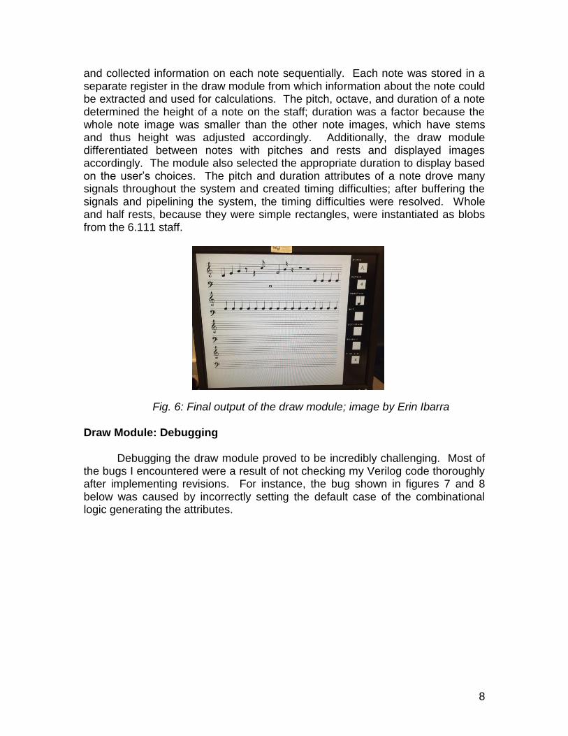
Draw Module: Debugging Debugging the draw module proved to be incredibly challenging. Most of the bugs I encountered were a result of not checking my Verilog code thoroughly after implementing revisions. For instance, the bug shown in figures 7 and 8 below was caused by incorrectly setting the default case of the combinational logic generating the attributes.
9
Fig. 7, 8: Incorrect output of logic generating the attribute text and incorrect display of octave attribute; images by Erin Ibarra
At the time, I had set the default output of the attribute text logic to be “pitch”, which caused it to be displayed over the entirety of the toolbar. A similar error occurred later with the octave attribute. I also discovered that my system could not match the speed of the 65MHz clock that that the project utilized. I needed to pipeline and buffer signals appropriately in order for the system to output clean images to the VGA. Draw Module: Analysis and Recommendations The draw module is a large, complex module that integrates the entirety of the display in one location. As such, it should be approached with care and attention to detail. I could have detected many of my errors sooner had I been more careful when changing my Verilog code. Additionally, I would recommend pipelining a system this large from the start. I did not anticipate a problem that affected the overall aesthetics of the project and was unable to find a solution until the end of the project period. Overall, I felt that the drawing module was largely successful. The final module was pipelined and all images appeared
10
clearly on screen. While a few images were not completely flawless, overall the final product looked as I had predicted. Memories: Implementation I utilized 3 types of memory for the Digital Debussy system: BRAM and Read Only Memory (ROM) generated by the ISE LogiCORE Generator and the “mybram” module developed by the 6.111 staff. The display BRAM and the image ROMs were generated by LogiCORE and the shared BRAM utilized the “mybram” module. Memories: Debugging, Analysis, and Recommendations There was minimal debugging with the memories. Overall, I felt that the scheme I used was effective, but I could have found ways to cut down the amount of memory I utilized. Because the draw module accessed the memory continuously, I needed to create a separate BRAM for use by the control FSM and the playback module. I found that the ROMs were a simple way to add complex images to the graphical user interface as well.
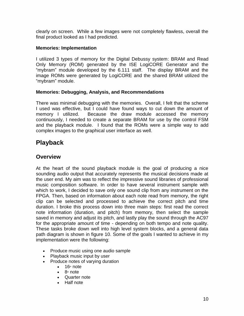
Playback Overview At the heart of the sound playback module is the goal of producing a nice sounding audio output that accurately represents the musical decisions made at the user end. My aim was to reflect the impressive sound libraries of professional music composition software. In order to have several instrument sample with which to work, I decided to save only one sound clip from any instrument on the FPGA. Then, based on information about each note read from memory, the right clip can be selected and processed to achieve the correct pitch and time duration. I broke this process down into three main steps: first read the correct note information (duration, and pitch) from memory, then select the sample saved in memory and adjust its pitch, and lastly play the sound through the AC97 for the appropriate amount of time - depending on both tempo and note quality. These tasks broke down well into high level system blocks, and a general data path diagram is shown in figure 10. Some of the goals I wanted to achieve in my implementation were the following:
Produce music using one audio sample Playback music input by user Produce notes of varying duration
16th note 8th note Quarter note Half note
11
Whole note Produce notes within a 2 octave range Play music at 3 tempos
Fig. 9 A high level overview of the organization of the playback module
Playback and Pitch Shifting: Phase Vocoder Theory
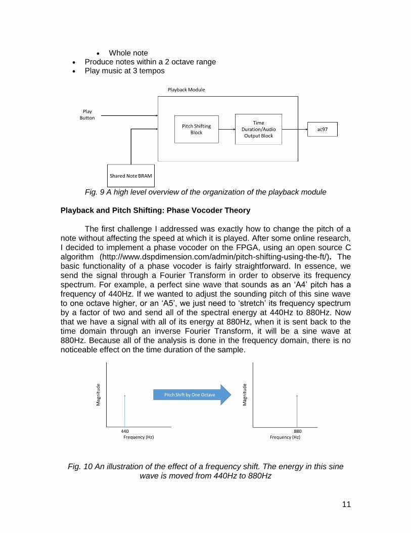
The first challenge I addressed was exactly how to change the pitch of a note without affecting the speed at which it is played. After some online research, I decided to implement a phase vocoder on the FPGA, using an open source C algorithm (http://www.dspdimension.com/admin/pitch-shifting-using-the-ft/). The basic functionality of a phase vocoder is fairly straightforward. In essence, we send the signal through a Fourier Transform in order to observe its frequency spectrum. For example, a perfect sine wave that sounds as an ‘A4’ pitch has a frequency of 440Hz. If we wanted to adjust the sounding pitch of this sine wave to one octave higher, or an ‘A5’, we just need to ‘stretch’ its frequency spectrum by a factor of two and send all of the spectral energy at 440Hz to 880Hz. Now that we have a signal with all of its energy at 880Hz, when it is sent back to the time domain through an inverse Fourier Transform, it will be a sine wave at 880Hz. Because all of the analysis is done in the frequency domain, there is no noticeable effect on the time duration of the sample.
Fig. 10 An illustration of the effect of a frequency shift. The energy in this sine wave is moved from 440Hz to 880Hz
12
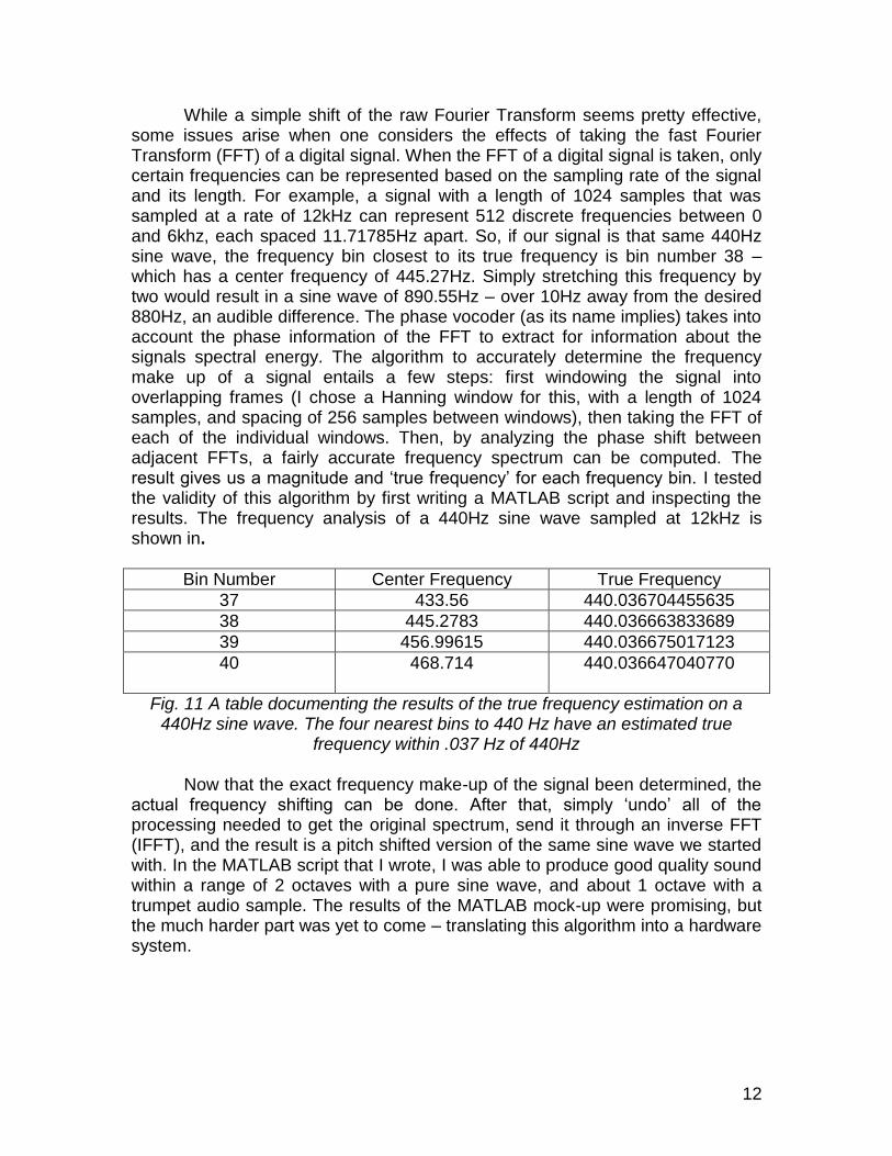
While a simple shift of the raw Fourier Transform seems pretty effective, some issues arise when one considers the effects of taking the fast Fourier Transform (FFT) of a digital signal. When the FFT of a digital signal is taken, only certain frequencies can be represented based on the sampling rate of the signal and its length. For example, a signal with a length of 1024 samples that was sampled at a rate of 12kHz can represent 512 discrete frequencies between 0 and 6khz, each spaced 11.71785Hz apart. So, if our signal is that same 440Hz sine wave, the frequency bin closest to its true frequency is bin number 38 – which has a center frequency of 445.27Hz. Simply stretching this frequency by two would result in a sine wave of 890.55Hz – over 10Hz away from the desired 880Hz, an audible difference. The phase vocoder (as its name implies) takes into account the phase information of the FFT to extract for information about the signals spectral energy. The algorithm to accurately determine the frequency make up of a signal entails a few steps: first windowing the signal into overlapping frames (I chose a Hanning window for this, with a length of 1024 samples, and spacing of 256 samples between windows), then taking the FFT of each of the individual windows. Then, by analyzing the phase shift between adjacent FFTs, a fairly accurate frequency spectrum can be computed. The result gives us a magnitude and ‘true frequency’ for each frequency bin. I tested the validity of this algorithm by first writing a MATLAB script and inspecting the results. The frequency analysis of a 440Hz sine wave sampled at 12kHz is shown in.
Bin Number Center Frequency True Frequency
37 433.56 440.036704455635
38 445.2783 440.036663833689
39 456.99615 440.036675017123
40 468.714 440.036647040770
Fig. 11 A table documenting the results of the true frequency estimation on a 440Hz sine wave. The four nearest bins to 440 Hz have an estimated true
frequency within .037 Hz of 440Hz Now that the exact frequency make-up of the signal been determined, the actual frequency shifting can be done. After that, simply ‘undo’ all of the processing needed to get the original spectrum, send it through an inverse FFT (IFFT), and the result is a pitch shifted version of the same sine wave we started with. In the MATLAB script that I wrote, I was able to produce good quality sound within a range of 2 octaves with a pure sine wave, and about 1 octave with a trumpet audio sample. The results of the MATLAB mock-up were promising, but the much harder part was yet to come – translating this algorithm into a hardware system.
13
Playback: Hardware Approach
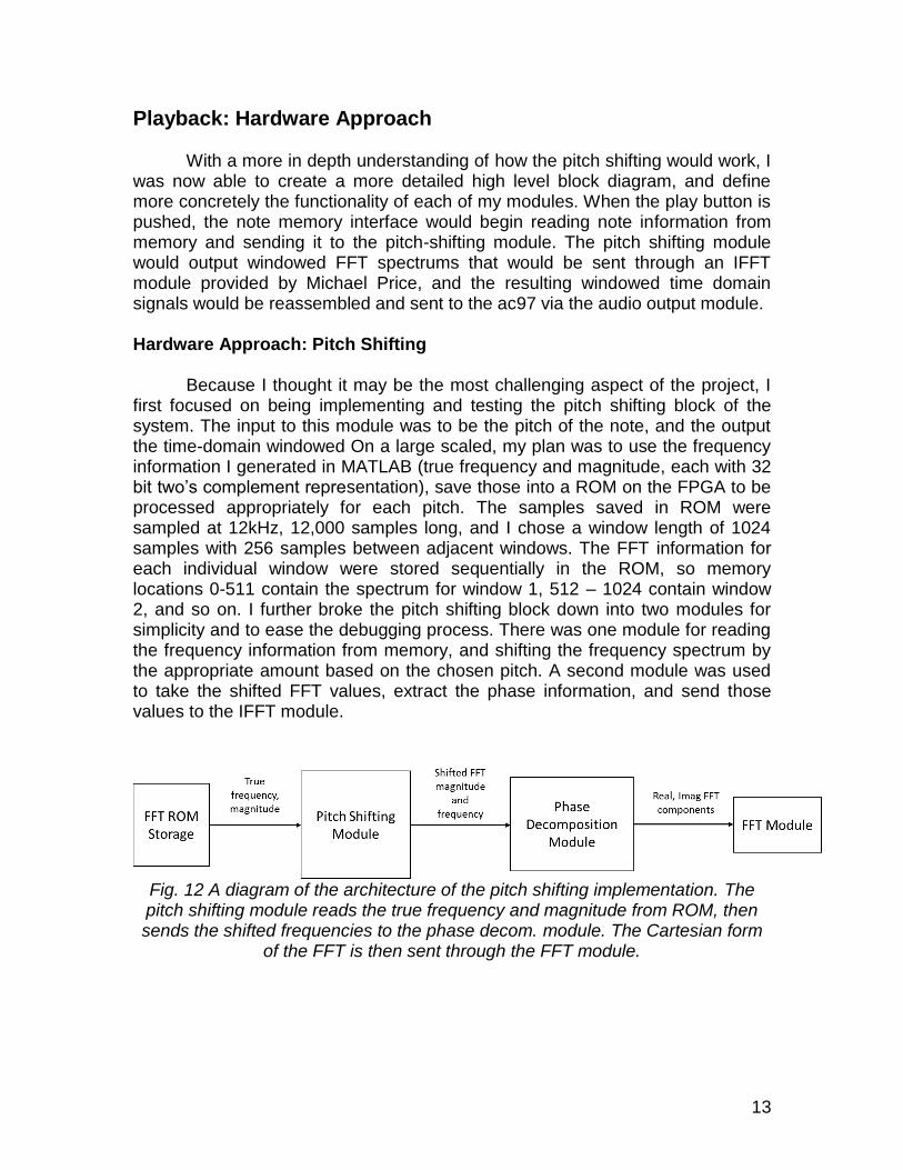
With a more in depth understanding of how the pitch shifting would work, I was now able to create a more detailed high level block diagram, and define more concretely the functionality of each of my modules. When the play button is pushed, the note memory interface would begin reading note information from memory and sending it to the pitch-shifting module. The pitch shifting module would output windowed FFT spectrums that would be sent through an IFFT module provided by Michael Price, and the resulting windowed time domain signals would be reassembled and sent to the ac97 via the audio output module. Hardware Approach: Pitch Shifting
Because I thought it may be the most challenging aspect of the project, I first focused on being implementing and testing the pitch shifting block of the system. The input to this module was to be the pitch of the note, and the output the time-domain windowed On a large scaled, my plan was to use the frequency information I generated in MATLAB (true frequency and magnitude, each with 32 bit two’s complement representation), save those into a ROM on the FPGA to be processed appropriately for each pitch. The samples saved in ROM were sampled at 12kHz, 12,000 samples long, and I chose a window length of 1024 samples with 256 samples between adjacent windows. The FFT information for each individual window were stored sequentially in the ROM, so memory locations 0-511 contain the spectrum for window 1, 512 – 1024 contain window 2, and so on. I further broke the pitch shifting block down into two modules for simplicity and to ease the debugging process. There was one module for reading the frequency information from memory, and shifting the frequency spectrum by the appropriate amount based on the chosen pitch. A second module was used to take the shifted FFT values, extract the phase information, and send those values to the IFFT module.
Fig. 12 A diagram of the architecture of the pitch shifting implementation. The pitch shifting module reads the true frequency and magnitude from ROM, then sends the shifted frequencies to the phase decom. module. The Cartesian form
of the FFT is then sent through the FFT module.
14
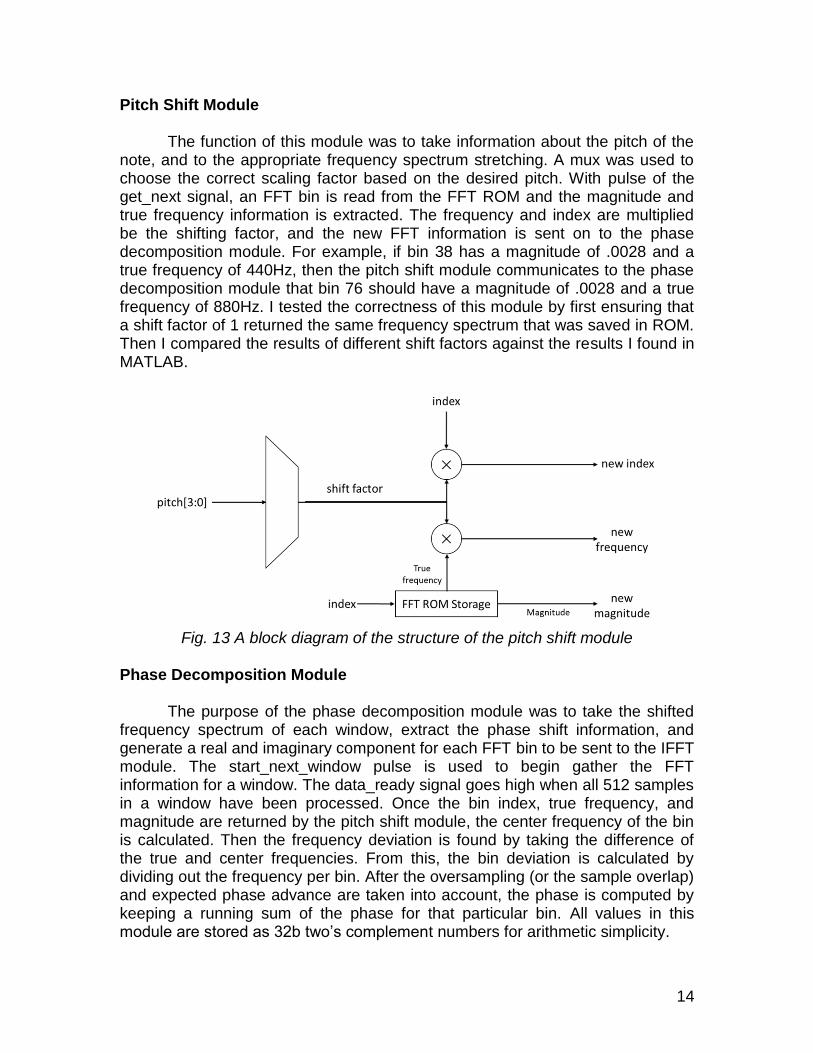
Pitch Shift Module
The function of this module was to take information about the pitch of the note, and to the appropriate frequency spectrum stretching. A mux was used to choose the correct scaling factor based on the desired pitch. With pulse of the get_next signal, an FFT bin is read from the FFT ROM and the magnitude and true frequency information is extracted. The frequency and index are multiplied be the shifting factor, and the new FFT information is sent on to the phase decomposition module. For example, if bin 38 has a magnitude of .0028 and a true frequency of 440Hz, then the pitch shift module communicates to the phase decomposition module that bin 76 should have a magnitude of .0028 and a true frequency of 880Hz. I tested the correctness of this module by first ensuring that a shift factor of 1 returned the same frequency spectrum that was saved in ROM. Then I compared the results of different shift factors against the results I found in MATLAB.
Fig. 13 A block diagram of the structure of the pitch shift module
Phase Decomposition Module
The purpose of the phase decomposition module was to take the shifted frequency spectrum of each window, extract the phase shift information, and generate a real and imaginary component for each FFT bin to be sent to the IFFT module. The start_next_window pulse is used to begin gather the FFT information for a window. The data_ready signal goes high when all 512 samples in a window have been processed. Once the bin index, true frequency, and magnitude are returned by the pitch shift module, the center frequency of the bin is calculated. Then the frequency deviation is found by taking the difference of the true and center frequencies. From this, the bin deviation is calculated by dividing out the frequency per bin. After the oversampling (or the sample overlap) and expected phase advance are taken into account, the phase is computed by keeping a running sum of the phase for that particular bin. All values in this module are stored as 32b two’s complement numbers for arithmetic simplicity.
15
Now that the phase and magnitude of the bin are known, they must be
returned to Cartesian coordinates so that they can be processed by the IFFT module. I used a CoreGen generated 1024 location 18bit two’s complement sin/cos LUT to take the sin and cosine of the phase, and used an algorithm to properly map the phase into a 0-2π interval. The calculated real and imaginary components are divided by 16 to account for scaling that was done when the bin magnitudes were written to ROM.
The phase sums are stored in a 32 bit wide, 512 location BRAM as are the magnitude sums. On my first pass making this module, I found that my calculations were off because the values I was reading from RAM were not stable. In order to make sure the correct phase and magnitude sums were written/read to memory, I used a couple of buffer registers and a cycle counter to carefully control the read/write process.
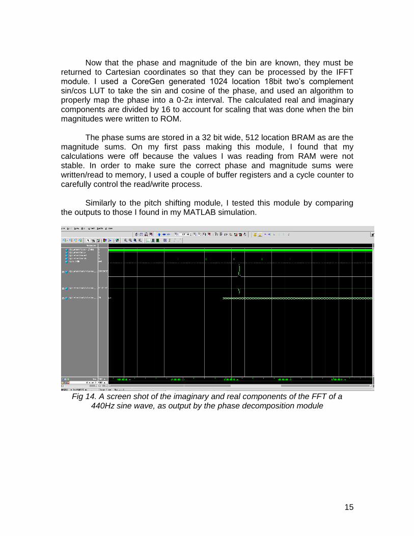
Similarly to the pitch shifting module, I tested this module by comparing the outputs to those I found in my MATLAB simulation.
Fig 14. A screen shot of the imaginary and real components of the FFT of a
440Hz sine wave, as output by the phase decomposition module
16
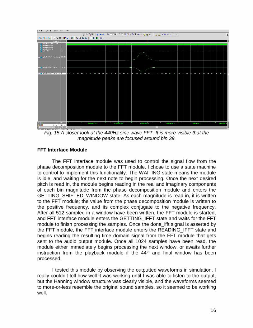
Fig. 15 A closer look at the 440Hz sine wave FFT. It is more visible that the
magnitude peaks are focused around bin 39. FFT Interface Module
The FFT interface module was used to control the signal flow from the phase decomposition module to the FFT module. I chose to use a state machine to control to implement this functionality. The WAITING state means the module is idle, and waiting for the next note to begin processing. Once the next desired pitch is read in, the module begins reading in the real and imaginary components of each bin magnitude from the phase decomposition module and enters the GETTING_SHIFTED_WINDOW state. As each magnitude is read in, it is written to the FFT module; the value from the phase decomposition module is written to the positive frequency, and its complex conjugate to the negative frequency. After all 512 sampled in a window have been written, the FFT module is started, and FFT interface module enters the GETTING_IFFT state and waits for the FFT module to finish processing the samples. Once the done_ifft signal is asserted by the FFT module, the FFT interface module enters the READING_IFFT state and begins reading the resulting time domain signal from the FFT module that gets sent to the audio output module. Once all 1024 samples have been read, the module either immediately begins processing the next window, or awaits further instruction from the playback module if the 44th and final window has been processed.
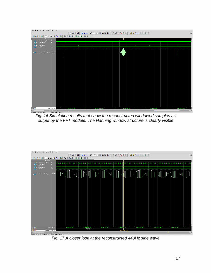
I tested this module by observing the outputted waveforms in simulation. I really couldn’t tell how well it was working until I was able to listen to the output, but the Hanning window structure was clearly visible, and the waveforms seemed to more-or-less resemble the original sound samples, so it seemed to be working well.
17
Fig. 16 Simulation results that show the reconstructed windowed samples as
output by the FFT module. The Hanning window structure is clearly visible
Fig. 17 A closer look at the reconstructed 440Hz sine wave
18
Audio Output Module
The audio output module was used to take the time domain windowed samples from the IFFT, reconstruct the sound clip, and send it to the AC97. Its jobs were to overlap the windows, and loop the sound clip for the appropriate amount of time. The biggest challenge of this module was properly overlapping adjacent windows. My original plan was to have an 18 bit wide, 1024 location BRAM to store the sound clip and overlap the samples as they were read in from the IFFT. But, I found this difficult because the output from the IFFT came in one burst, or at 1 sample per clock cycle. Because each point in the sound clip is represented in 4 different windows, I would need 2 clock cycles to process each sample: 1 clock cycle to read in the current location value, and another to add it to the value from the IFFT and then rewrite that to the BRAM. I found this particularly challenging, so I decided instead to just create a (very large, with 45k locations) BRAM to store all of the windows sequentially, then do the overlapping as data was sent to the AC97 - during the times when data wasn’t being received from the IFFT. Unfortunately, this scheme wasn’t much easier to implement, and also maxed out the BRAM availability on the FPGA if I were to conserve the 18bit two’s complement structure that I desired for the sound.
In the end, I wasn’t able to successfully complete this module that was pretty essential to my goals. With more time, I would have spent more time trying to work out my original implementation idea for this module.
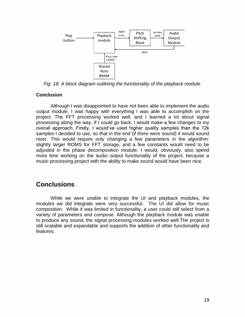
Playback Module
The playback module was used to connect together the pitch shifting block, audio output module, and note memory. When the play button is held down, this module would control the sample processing until either the song ends or the play button is released. I decided to first put together the pitch shifting and audio output blocks because, although I had compared the output of my pitch shifting block to the results I found in MATLAB, the true test of their functionality would be to actually listen to the resulting sounds. After being able to reliable play just one note at a time, my plan was to then add in the ability to parse in notes from note BRAM shared with the UI module. But, because I ran into trouble with the audio output module, I never got around to adding in that functionality. However, with the control signals built into the pitch shift modules, I think it would have been fairly straight forward. Once a note had been fully processed and sent to the audio output module, the next note could be read from memory and begin to be processed by the pitch shifting block.
19
Fig. 18. A block diagram outlining the functionality of the playback module.
Conclusion
Although I was disappointed to have not been able to implement the audio output module, I was happy with everything I was able to accomplish on the project. The FFT processing worked well, and I learned a lot about signal processing along the way. If I could go back, I would make a few changes to my overall approach. Firstly, I would’ve used higher quality samples than the 12k samples I decided to use, so that in the end (if there were sound) it would sound nicer. This would require only changing a few parameters in the algorithm: slightly larger ROMS for FFT storage, and a few constants would need to be adjusted in the phase decomposition module. I would, obviously, also spend more time working on the audio output functionality of the project, because a music processing project with the ability to make sound would have been nice.
Conclusions
While we were unable to integrate the UI and playback modules, the modules we did integrate were very successful. The UI did allow for music composition. While it was limited in functionality, a user could still select from a variety of parameters and compose. Although the playback module was unable to produce any sound, the signal processing modules worked well.The project is still scalable and expandable and supports the addition of other functionality and features.