Embed Size (px)
Citation preview

PEROVSKITES
Perovskite-type Mn2O3 described by S. V. Ovsyannikov and co-workers on page 8185, is a unique, hard semiconductor having a narrow and direct bandgap of 0.45 eV and switchable p-n electrical conduction. Pv-Mn2O3, comprising nontoxic and inexpensive elements, is much stronger than traditional semiconductors, and promises applications in the semiconductor industry, e.g., in IR detectors and other devices.
ADMA-26-48-Frontispiece.indd 1 12/1/14 6:44 PM
© 2014 WILEY-VCH Verlag GmbH & Co. KGaA, Weinheim 8185wileyonlinelibrary.com
CO
MM
UN
ICATIO
N
A Hard Oxide Semiconductor with A Direct and Narrow Bandgap and Switchable p–n Electrical Conduction
Sergey V. Ovsyannikov ,* Alexander E. Karkin , Natalia V. Morozova , Vladimir V. Shchennikov , Elena Bykova , Artem M. Abakumov , Alexander A. Tsirlin , Konstantin V. Glazyrin , and Leonid Dubrovinsky
Dr. S. V. Ovsyannikov, E. Bykova, Dr. K. V. Glazyrin, Prof. L. S. Dubrovinsky Bayerisches Geoinstitut Universität Bayreuth Universitätsstrasse 30 , D-95447 Bayreuth , Germany E-mail: [email protected] Dr. A. E. Karkin, N. V. Morozova, Prof. V. V. Shchennikov Institute of Metal PhysicsRussian Academy of Sciences Urals Division GSP-170, 18 S. Kovalevskaya Str. , Yekaterinburg 620219 , Russia E. Bykova Laboratory of Crystallography Universität Bayreuth D-95440 , Bayreuth , Germany Prof. A. M. Abakumov Electron Microscopy for Materials Research (EMAT) University of Antwerp Groenenborgerlaan 171 , B-2020 Antwerp , Belgium Dr. A. A. Tsirlin National Institute of Chemical Physics and Biophysics Akadeemia tee 23 , 12618 Tallinn , Estonia Dr. K. V. Glazyrin Petra III, P02, Deutsches Elektronen Synchrotron Notkestr. 85 , 22607 Hamburg , Germany
DOI: 10.1002/adma.201403304
systems with advanced properties or unusual electron band structure features may, in turn, lead to emergent industrial appli-cations. The overwhelming majority of existing industrial semi-conductor devices is based on solid solutions, doped modifi ca-tions, and heterostructures of a number of basic semiconductors that are distinguished by electronic, chemical, mechanical and other properties. Extending the list of the basic semiconductors remains one of primary goals for semiconductor science and technology. For instance, it is worth mentioning recent advances in fabrication of multifunctional hard wide-bandgap semicon-ductors, like A N3
IV4 (A IV – Si, Sn, Ge, Zr, Hf) with tunable opto-
electronic properties, [ 1–4 ] comparable with those of In 1− x Ga x N. [ 5 ] High-pressure high-temperature (HP-HT) synthesis is
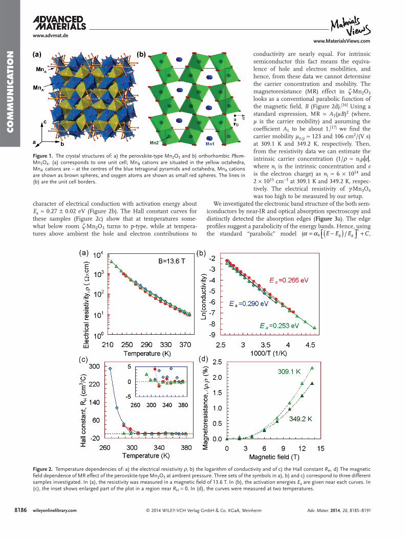
known to be a powerful tool for preparation of new unique materials and phases of which properties can be very different from those of their ambient pressure analogues. In this work we examined the properties of two high-pressure polymorphs of manganese oxides, perovskite-type ζ-Mn 2 O 3 , [ 6 ] and marokite-type Mn 3 O 4 [ 7 ] (may be labeled as γ-Mn 3 O 4 after hausmannite, α-Mn 3 O 4 and cubic spinel, β-Mn 3 O 4 ). The γ-Mn 3 O 4 polymorph was discovered several decades ago; [ 8 ] it was found to crystallize in the orthorhombic CaMn 2 O 3 (marokite)-type structure, [ 9,10 ] and to show anti-ferromagnetic ordering below 210 K. [ 11 ] Very recently a recoverable at ambient conditions ζ-Mn 2 O 3 with a double-perovskite-type structure with intricate electronic con-fi guration, Mn 2+ (Mn 3+ ) 3 (Mn 3.25+ ) 4 O 12 has been revealed. [ 6 ] The ζ-Mn 2 O 3 polymorph has a triclinic distortion (space group F 1, # 2, P 1 in the standard settings) ( Figure 1 a), and fi ne details of its crystal structure are yet to be studied. Both polymorphs, per-ovskite-type ζ-Mn 2 O 3 and marokite-type γ-Mn 3 O 4 are consider-ably denser than the ambient-pressure α - Mn 2 O 3 and α-Mn 3 O 4 phases, [ 12–15 ] and therefore, they could demonstrate new phys-ical characteristics for these oxides. Since the magnetic proper-ties of these polymorphs were recently reported, [ 6,11 ] in the pre-sent work we investigate their optical and electronic transport properties by means of near-infrared and optical absorption spectroscopy, by Raman spectroscopy and by measurements of the electrical resistivity. The case of ζ-Mn 2 O 3 appears to be more spectacular, and, in addition, we examine its mechanical properties by means of compressibility study and Vickers hard-ness testing. Furthermore, we probe the evolution of the elec-tronic transport properties of ζ-Mn 2 O 3 upon compression.
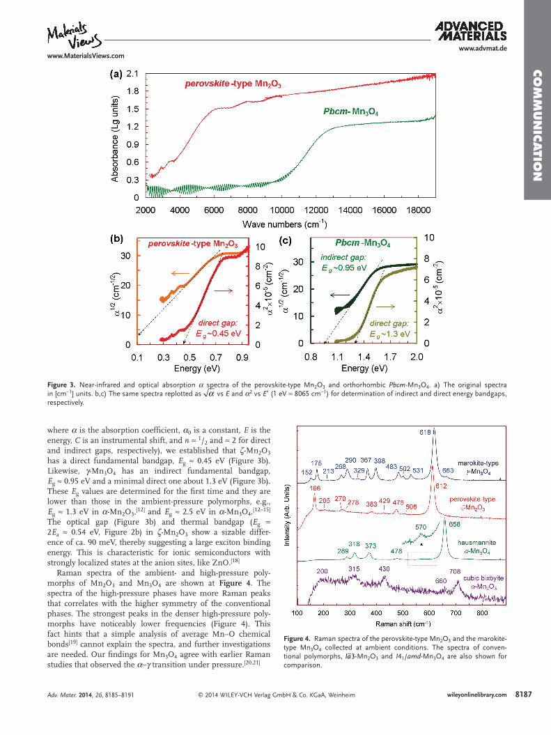
The temperature dependencies of the electrical resistivity were investigated on three bulk samples of pure ζ-Mn 2 O 3 ( Figure 2 a) synthesized at slightly different HP-HT condi-tions in the stability region of this phase. [ 6 ] These curves unambiguously suggest an intrinsic semiconducting
Chemical bonding in inorganic solids partly predetermines and interconnects their elastic and electronic properties; metals are usually plastic, semiconductors are brittle, and insulating ceramics may be rather hard. Overplaying the combination of these proper-ties could greatly extend the applicability of materials for indus-trial use. Here we report an oxide semiconductor (perovskite-type Mn 2 O 3 ) having a narrow and direct bandgap of 0.45 eV and a high Vickers hardness of 15 GPa. All the known materials with resem-bling electronic band structures (e.g., InSb, PbTe, PbSe, PbS, and InAs) play crucial roles in the semiconductor industry, e.g., in IR detectors, thermal image detectors, photodiodes or photo-elec-tromagnetic detectors, and in other devices. The perovskite-type Mn 2 O 3 comprising nontoxic, earth-abundant and inexpensive elements, is much more incompressible and stronger than the above semiconductors, and unique combination of its electronic and mechanical properties makes it particularly promising. Fur-thermore, we show that applied pressure (stress) can reversibly or irreversibly (in dependence on pressure value) ‘switch’ the elec-trical conduction type of perovskite-type Mn 2 O 3 .
Development of semiconductor technologies is closely related to advances in materials science and engineering. Modern technological challenges require designing and creating novel unique and “smart” materials. Newly fabricated semiconductor
Adv. Mater. 2014, 26, 8185–8191
www.advmat.dewww.MaterialsViews.com
8186 wileyonlinelibrary.com © 2014 WILEY-VCH Verlag GmbH & Co. KGaA, Weinheim
CO
MM
UN
ICATI
ON
character of electrical conduction with activation energy about E a ≈ 0.27 ± 0.02 eV (Figure 2 b). The Hall constant curves for these samples (Figure 2 c) show that at temperatures some-what below room ζ-Mn 2 O 3 turns to p-type, while at tempera-tures above ambient the hole and electron contributions to
conductivity are nearly equal. For intrinsic semiconductor this fact means the equiva-lence of hole and electron mobilities, and hence, from these data we cannot determine the carrier concentration and mobility. The magnetoresistance (MR) effect in ζ-Mn 2 O 3 looks as a conventional parabolic function of the magnetic fi eld, B (Figure 2 d). [ 16 ] Using a standard expression, MR = A 1 ( µB ) 2 (where, µ is the carrier mobility) and assuming the coeffi cient A 1 to be about 1, [ 17 ] we fi nd the carrier mobility µ n,p ≈ 123 and 106 cm 2 /(V s) at 309.1 K and 349.2 K, respectively. Then, from the resistivity data we can estimate the intrinsic carrier concentration (1/ ρ ≈ n i µ � e �, where n i is the intrinsic concentration and e is the electron charge) as n i ≈ 6 × 10 14 and 2 × 10 15 cm −3 at 309.1 K and 349.2 K, respec-tively. The electrical resistivity of γ-Mn 3 O 4 was too high to be measured by our setup.
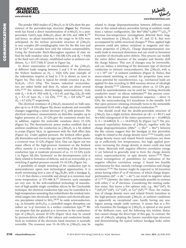
We investigated the electronic band structure of the both sem-iconductors by near-IR and optical absorption spectroscopy and distinctly detected the absorption edges ( Figure 3 a). The edge profi les suggest a parabolicity of the energy bands. Hence, using the standard “parabolic” model ( E E E C
n/0 g gα α ( )= −⎡⎣ ⎤⎦ + ,
Adv. Mater. 2014, 26, 8185–8191
www.advmat.dewww.MaterialsViews.com
Figure 1. The crystal structures of: a) the perovskite-type Mn 2 O 3 and b) orthorhombic Pbcm -Mn 3 O 4 . (a) corresponds to one unit cell; Mn B cations are situated in the yellow octahedra, Mn A’ cations are – at the centres of the blue tetragonal pyramids and octahedra, Mn A cations are shown as brown spheres, and oxygen atoms are shown as small red spheres. The lines in (b) are the unit cell borders.
Figure 2. Temperature dependencies of: a) the electrical resistivity ρ , b) the logarithm of conductivity and of c) the Hall constant R H . d) The magnetic fi eld dependence of MR effect of the perovskite-type Mn 2 O 3 at ambient pressure. Three sets of the symbols in a), b) and c) correspond to three different samples investigated. In (a), the resistivity was measured in a magnetic fi eld of 13.6 T. In (b), the activation energies E a are given near each curves. In (c), the inset shows enlarged part of the plot in a region near R H = 0. In (d), the curves were measured at two temperatures.
8187wileyonlinelibrary.com© 2014 WILEY-VCH Verlag GmbH & Co. KGaA, Weinheim
CO
MM
UN
ICATIO
N
where α is the absorption coeffi cient, α 0 is a constant, E is the energy, C is an instrumental shift, and n ≈ 1 / 2 and ≈ 2 for direct and indirect gaps, respectively), we established that ζ-Mn 2 O 3 has a direct fundamental bandgap, E g ≈ 0.45 eV (Figure 3 b). Likewise, γ-Mn 3 O 4 has an indirect fundamental bandgap, E g ≈ 0.95 eV and a minimal direct one about 1.3 eV (Figure 3 b). These E g values are determined for the fi rst time and they are lower than those in the ambient-pressure polymorphs, e.g., E g ≈ 1.3 eV in α-Mn 2 O 3 , [ 12 ] and E g ≈ 2.5 eV in α-Mn 3 O 4 . [ 12–15 ] The optical gap (Figure 3 b) and thermal bandgap ( E g = 2 E a ≈ 0.54 eV, Figure 2 b) in ζ-Mn 2 O 3 show a sizable differ-ence of ca. 90 meV, thereby suggesting a large exciton binding energy. This is characteristic for ionic semiconductors with strongly localized states at the anion sites, like ZnO. [ 18 ]
Raman spectra of the ambient- and high-pressure poly-morphs of Mn 2 O 3 and Mn 3 O 4 are shown at Figure 4 . The spectra of the high-pressure phases have more Raman peaks that correlates with the higher symmetry of the conventional phases. The strongest peaks in the denser high-pressure poly-morphs have noticeably lower frequencies (Figure 4 ). This fact hints that a simple analysis of average Mn–O chemical bonds [ 19 ] cannot explain the spectra, and further investigations are needed. Our fi ndings for Mn 3 O 4 agree with earlier Raman studies that observed the α–γ transition under pressure. [ 20,21 ]
Adv. Mater. 2014, 26, 8185–8191
www.advmat.dewww.MaterialsViews.com
Figure 3. Near-infrared and optical absorption α spectra of the perovskite-type Mn 2 O 3 and orthorhombic Pbcm -Mn 3 O 4 . a) The original spectra in [cm −1 ] units. b,c) The same spectra replotted as α vs E and α 2 vs E ′ (1 eV ≈ 8065 cm −1 ) for determination of indirect and direct energy bandgaps, respectively.
Figure 4. Raman spectra of the perovskite-type Mn 2 O 3 and the marokite-type Mn 3 O 4 collected at ambient conditions. The spectra of conven-tional polymorphs, Ia3-Mn 2 O 3 and I 4 1 / amd -Mn 3 O 4 are also shown for comparison.
8188 wileyonlinelibrary.com © 2014 WILEY-VCH Verlag GmbH & Co. KGaA, Weinheim
CO
MM
UN
ICATI
ON The powder XRD studies of ζ-Mn 2 O 3 to 16 GPa show the per-
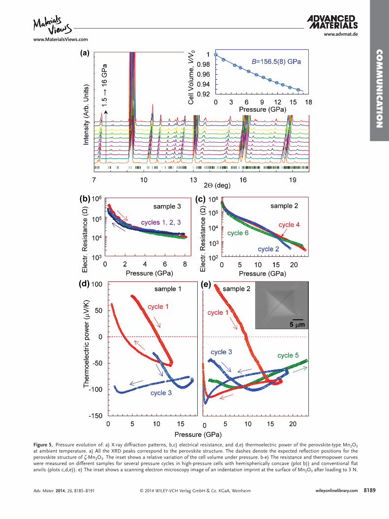
sistence of the perovskite-type structure ( Figure 5 a). Previous work has found a direct transformation of α - Mn 2 O 3 to a post-perovskite CaIrO 3 -type δ - Mn 2 O 3 above 28 GPa and 1000 K, [ 22 ] and hence, no phase transitions in the range to 16 GPa were anticipated. As the triclinic perovskite structure of ζ-Mn 2 O 3 is very complex (20 crystallographic sites for the Mn ions and 24 for O), [ 6 ] we consider here only the volume compressibility. Using the third-order Birch-Murnaghan equation of state we fi nd the bulk modulus value B 0 = 156.5(8) GPa and B 0 ′ = 9.4(4) at the fi xed unit cell volume, established earlier at ambient con-ditions, V 0 = 3157.73(9) Å 3 (inset in Figure 5 a).
In direct examination of microhardness of the ζ-Mn 2 O 3 at different loads ranging between 2 and 5 N we determine the Vickers hardness as H V ≈ 15(2) GPa (one example of the indentation imprint at load to 3 N is shown as inset in Figure 5 e). This value is typical for nitride ceramics (e.g., for Si 3 N 4 H V ≈15.5 GPa). The known industrial semiconduc-tors are rather brittle and their H V values are about several GPa. [ 23,24 ] For instance, direct-bandgap semiconductors, InAs with E g ≈ 0.36 eV, PbS with E g ≈ 0.4 eV, and Hg 0.7 Cd 0.3 Te with E g ≈ 0.3 eV have H V ≈ 2.6 GPa, [ 23,24 ] H V ≈ 0.8 GPa, [ 25 ] and H V ≈ 0.7 GPa, [ 26 ] respectively.
The electrical resistance of ζ-Mn 2 O 3 measured on bulk sam-ples up to ca. 8 GPa (Figure 5 b) shows moderate and reversible changes suggesting a minor decrease of E g with pressure. The electrical resistance measurements on thin-fi lm samples up to higher pressures of ca. 23 GPa give the consistent results but, in addition, register the noticeable variations above 15 GPa (Figure 5 c). The thermoelectric power studies establish that at ambient conditions the conduction in ζ-Mn 2 O 3 is a bit shifted to p -type (Figure 5 d,e), in agreement with the Hall effect data (Figure 2 c). Under applied pressure, the Seebeck effect gradu-ally diminishes and inverts its sign near 10 GPa, and then shows a crossover near 15 GPa (Figure 5 d,e). One can fi gure out two major effects of the high-pressure treatment on the Seebeck effect, namely: i) a reversible p–n switching of the dominant conduction type at moderate pressures of ca. 11–13 GPa (cycle 1 in Figure 5 d) (the ‘hysteresis’ on the decompression cycle is likely related to formation of defects), and ii) an irreversible p–n switching if applied pressure exceeds 15–16 GPa (Figure 5 e).
A possibility of simple switching of the conduction type in semiconductors opens new technological opportunities. It is worth mentioning here a case of Ag 10 Te 4 Br 3 with a bandgap E g ≈ 1.1 eV that shows a reversible and abrupt p–n inversion near room temperature, at 375–400 K. [ 27 ] However, such examples are very rare. In the well-established technology of manufac-ture of high-quality single crystalline silicon by the Czochralski technique, the electrical conduction type may be controlled by a high-temperature annealing that redistributes the residual inter-stitial oxygen into electrically active clusters and electrically-pas-sive precipitates related to SiO 2 . [ 28,29 ] In oxide semiconductors, e.g., in hematite (α-Fe 2 O 3 ), a controlled oxygen absorption can induce an ‘n–p’ inversion in a surface conduction type. [ 30 ] We can propose that the gradual p–n inversion in the conduction-type of ζ-Mn 2 O 3 around 10 GPa (Figure 5 d,e) may be caused by pressure-driven shifts of the valence and conduction bands. Such an evolution of the electronic band structure is normally reversible. The crossover near 15–16 GPa in ζ-Mn 2 O 3 may be
related to charge disproportionation between different cation sites in this mixed-valence perovskite having at ambient condi-tions a valence confi guration, like Mn 2+ (Mn 3+ ) 3 (Mn 3.25+ ) 4 O 12 . [ 6 ] Previous low-temperature investigations detected three mag-netic transitions in ζ-Mn 2 O 3 at 99, 47, and 12 K, that were accompanied by subtle structural changes. [ 6 ] Thus, applied high pressure could also induce variations in magnetic and elec-tronic properties of ζ-Mn 2 O 3 . Charge disproportionation nor-mally leads to structural distortions and can result in formation a number of electrically-active defects. This process can modify the native defect structure of the samples and thereby shift the charge balance. This sort of changes may be irreversible, and can induce a switching of the dominant type of electrical conduction in intrinsic semiconductors, like ζ-Mn 2 O 3 with n i ≈ 6 × 10 14 cm −3 at ambient conditions (Figure 2 ). Notice, that stress-related switching or control the properties have enor-mous potential for nanoelectronics, e.g., mechanical loads are applied for data recording in IBM memory devices of ultrahigh storage density. [ 31,32 ] Likewise, stresses above ca. 12 GPa gen-erated by nanoindentation can be used for “writing electrically conductive zones” on silicon substrates; [ 33 ] this process corre-sponds to the known phase transitions sequence, – above 11 GPa, the semiconducting Si-I transforms to the metallic Si-II that upon pressure releasing eventually turns to the metastable semimetal Si-III with a high electrical conduction. [ 34 ]
One should recall that the double-perovskite structure of ζ-Mn 2 O 3 has a slight triclinic distortion ( α ≈ β ≈ γ ≈ 89.2°) and two-fold enlargement of the lattice parameters ( a = 14.6985(2) Å, b = 14.6482(2) Å, c = 14.6705(2) Å) (Figure 1 a). [ 6 ] The pro-nounced superlattice features of ζ-Mn 2 O 3 together with the charge disproportionation (2Mn 3+ → Mn 2+ + Mn 4+ ) between the Mn cations suggest that the bandgap in this perovskite might be related to the charge density wave. [ 35,36 ] Usually, such charge density waves and related Peierls transitions can show up at suffi ciently low temperatures, but high applied pres-sures increasing the charge density at atoms could also lead to them. Materials with negative effective correlation energy U are believed to generally tend to form the charge density waves, superconductivity, or spin density waves. [ 35,36 ] Theo-retical investigations of possibilities for realization of the negative effective correlation energy U found two feasible mechanisms for that, namely, exchange correlation and charge excitation. [ 35,36 ] The former might be expected in 3 d transition atoms having either d 4 or d 6 electrons, of which charge dispro-portionation (2 d n → d n −1 + d n +1 ) can result in negative values of U . [ 35,36 ] Likewise, the latter is potentially possible in systems with either s 1 or d 9 electrons. Considering the existing oxida-tion states, this leaves a few options only, e.g., Mn 3+ (3 d 4 ), Fe 4+ (3 d 4 ),Fe 2+ (3 d 6 ), Co 3+ (3 d 6 ), or Cu 2+ (3 d 9 ). [ 36 ] Thus, the realiza-tion of charge density wave and related Peierls transition in the high-pressure polymorph ζ-Mn 2 O 3 at ambient conditions is apparently an exceptional case, hardly having any ana-logues among simple oxide systems. It seems that at a Pei-erls transition the bandgap in ζ-Mn 2 O 3 is opened at one point of the Brillouin zone, and the following tiny triclinic distor-tion cannot change the direct-type of this gap. In contrast, the case of γ-Mn 3 O 4 adopting the known marokite-type structure and demonstrating the typical indirect bandgap looks rather regular.
Adv. Mater. 2014, 26, 8185–8191
www.advmat.dewww.MaterialsViews.com
8189wileyonlinelibrary.com© 2014 WILEY-VCH Verlag GmbH & Co. KGaA, Weinheim
CO
MM
UN
ICATIO
N
Adv. Mater. 2014, 26, 8185–8191
www.advmat.dewww.MaterialsViews.com
Figure 5. Pressure evolution of: a) X-ray diffraction patterns, b,c) electrical resistance, and d,e) thermoelectric power of the perovskite-type Mn 2 O 3 at ambient temperature. a) All the XRD peaks correspond to the perovskite structure. The dashes denote the expected refl ection positions for the perovskite structure of ζ-Mn 2 O 3 . The inset shows a relative variation of the cell volume under pressure. b-e) The resistance and thermopower curves were measured on different samples for several pressure cycles in high-pressure cells with hemispherically concave (plot b)) and conventional fl at anvils (plots c,d,e)). e) The inset shows a scanning electron microscopy image of an indentation imprint at the surface of Mn 2 O 3 after loading to 3 N.
8190 wileyonlinelibrary.com © 2014 WILEY-VCH Verlag GmbH & Co. KGaA, Weinheim
CO
MM
UN
ICATI
ON
Adv. Mater. 2014, 26, 8185–8191
www.advmat.dewww.MaterialsViews.com
The ζ-Mn 2 O 3 with the direct bandgap E g ≈ 0.45 eV remarkably complements the limited group of narrow- and direct-bandgap semiconductors that are of exceptional technological impor-tance; just to mention, such as: InSb ( E g ≈ 0.17 eV), [ 17 , 37 ] PbTe and PbSe ( E g ≈ 0.27 eV), [ 37,38 ] InAs ( E g ≈ 0.36 eV), [ 17 , 37 ] PbS ( E g ≈ 0.4 eV), [ 37,38 ] InN ( E g ≈ 0.7 eV), [ 39,40 ] and GaSb ( E g ≈ 0.73 eV), [ 17 , 37 ] and Hg 1− x Cd x Te solid solutions with tunable E g ≈ 0–1.5 eV. [ 41 ] Mn 2 O 3 comprises two nontoxic, earth-abundant and inexpensive elements, and thus, has an economical advantage over the above semiconductors consisting of scarce or/and toxic In, Pb, Cd, Hg, As, Te, Se, and other elements. Furthermore, ζ-Mn 2 O 3 is much more incompressible and stronger than the usual non-oxide semiconductors. The ‘softness’ of the above semiconductors is a serious obstacle hindering their industrial use. For instance, han-dling of ‘soft’ HdCdTe elements with the excellent electronic trans-port characteristics is known to be particularly diffi cult during a technological device process, [ 26 ] and hence, ‘hard’ semiconduc-tors with essentially similar electronic band structure will be in high demand. The unique properties of ζ-Mn 2 O 3 suggest that this material is promising for new industrial applications. Usu-ally, high-pressure application is well simulated in thin strained fi lms, [ 42 ] and hence, the perovskite-type ζ-Mn 2 O 3 might be poten-tially prepared just at ambient pressure conditions. In addition, a possibility of reversible and irreversible p–n switching of the dominant conduction type by applied pressure at room tempera-ture (Figure 5 d,e) indicates that ζ-Mn 2 O 3 has a potential as ‘smart’ material with remarkable opto-electro-mechanical characteristics.
In summary, we found that the ζ-Mn 2 O 3 and γ-Mn 3 O 4 polymorphs are narrow-bandgap semiconductors, unlike the wide-bandgap cubic-bixbyite α - Mn 2 O 3 , [ 12 ] and hausmannite α-Mn 3 O 4 . [ 12–15 ] We established that ζ-Mn 2 O 3 has a direct fundamental bandgap of E g ≈ 0.45 eV, likewise, γ-Mn 3 O 4 has an indirect fundamental bandgap of E g ≈ 0.95 eV and small direct gap of 1.3 eV. In examination of the elastic and plastic properties of ζ-Mn 2 O 3 , we determined the high values of bulk modulus, B 0 = 156.5(8) GPa (at B 0 ′ = 9.4(4)) and of Vickers hardness, H V = 15.2 GPa. A combination of the direct and narrow bandgap with a high Vickers hardness strongly suggests that ζ-Mn 2 O 3 may have important technological applications beyond those of the known ‘soft’ narrow-direct-bandgap semiconductors, like InSb, PbTe, PbSe, PbS, InAs, InN, and HgCdTe.
Experimental Section Sample Preparation and Characterization : The polycrystalline samples
of ζ-Mn 2 O 3 and single crystals of γ-Mn 3 O 4 were synthesized at HP-HT
conditions near 20 GPa and 1400–1700 °C. The chemical composition and morphology of the samples were examined by scanning electron microscopy (SEM) at a LEO-1530 instrument, and by microprobe analysis at a JEOL JXA-8200 electron microprobe.
X-ray Diffraction : Using single-crystal X-ray diffraction (XRD) data collected on a four-circle Oxford Diffraction Xcalibur diffractometer ( λ = 0.7107Å) equipped with an Xcalibur Sapphire2 CCD detector (see Supporting information for details), we confi rmed the CaMn 2 O 3 -type structure of γ-Mn 3 O 4 (Figure 1 b, Table 1 ). [ 9–11,13 ] Pure bulk samples of ζ-Mn 2 O 3 with the double-perovskite-type structure were selected for this work. The detailed analysis of the double-perovskite structure of ζ-Mn 2 O 3 was reported earlier. [ 6 ]
Electronic Transport Experiments : Electrical and galvanomagnetic properties of the samples were measured by a conventional Montgomery method (a modifi cation of the Van der Pauw method) using an Oxford Instruments setup. [ 43 ] The measurements were performed in magnetic fi elds up to 13.6 T.
Optical Experiments : Near-Infrared (IR) and optical absorption spectra were collected on double-side polished samples of thickness ca. 15 µm at Bruker IFS 120 Fourier transform spectrometer. [ 16 ] Raman spectra were excited with the 632.8 nm line of a He–Ne laser and recorded by a LabRam spectrometer in a back-scattering geometry.
High-Pressure Structural and Electronic Transport Experiments : In addition, we probed the structural and electronic stability of ζ-Mn 2 O 3 under high pressure. The structural behavior of ζ-Mn 2 O 3 was studied at the ID09a line of ESRF ( λ = 0.41481 Å) in diamond anvil cell with Re gasket with a hole fi lled with He pressure-transmitting medium. [ 44 ] The electrical and thermoelectric properties of ζ-Mn 2 O 3 were investigated at room temperature in two anvil-type cells with fl at and hemispherically concave anvils. [ 45 ] The cells were loaded in an automated mini-press setup allowing to tune applied stress continuously with simultaneous measurements of properties of a sample under multiple pressure cycling. [ 46 ] The electrical resistance was measured by quasi-four probe method, and the thermopower - by the same method as in previous works. [ 46 ]
Hardness : The mechanical hardness of the perovskite-type Mn 2 O 3 has been examined by microindentation under loads ranging between 2 and 5 N. We performed a series of tests at different points of well-polished samples and then averaged the results.
Supporting Information Supporting Information is available from the Wiley Online Library or from the author.
Acknowledgements The authors thank H. Keppler, V. Dmitriev and M. Hanfl and for assistance in the optical and structural experiments. S.V.O. thanks the Deutsche Forschungsgemeinschaft (DFG, project OV-110/1–2) for the
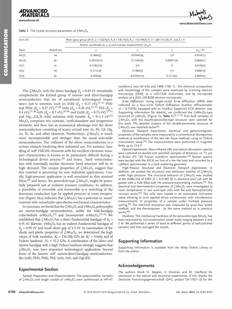
Table 1. The crystal structure parameters of γ-Mn 3 O 4 .
Unit cell: Pbcm space group (#57), a = 3.0276(1) Å, b = 9.8176(3) Å, c = 9.5799(3) Å, V = 284.751(16) Å 3 , and Z = 4
Atomic coordinates ( x , y , z ) and isotropic displacements ( U eq a ):
Atom Wykoff site x y z U eq a , Å 2
Mn(1) 4 d 0.1864(2) 0.85445(6) 1/4 0.0103(1)
Mn(2) 8 e 0.29434(13) 0.11463(4) 0.06957(4) 0.0069(1)
O(1) 4 c 0.1203(10) 3/4 0 0.0109(5)
O(2) 4 d 0.3115(9) 0.1980(3) 1/4 0.0085(4)
O(3) 8 e 0.2936(6) 0.47054(19) 0.1113(2) 0.0094(3)
8191wileyonlinelibrary.com© 2014 WILEY-VCH Verlag GmbH & Co. KGaA, Weinheim
CO
MM
UN
ICATIO
N
Adv. Mater. 2014, 26, 8185–8191
www.advmat.dewww.MaterialsViews.com
fi nancial support. A part of this work was performed as a part of the State Program «Potok» No. 01201463334 (Project No. 12-P-2-1004) and under fi nancial support of the Russian Foundation for Basic Research, RFBR (Project No. 14–02–00622a).
Received: July 22, 2014 Revised: September 17, 2014
Published online: October 27, 2014
[1] A. Zerr , R. Riedel , T. Sekine , J. E. Lowther , W.-Y. Ching , I. Tanaka , Adv. Mater. 2006 , 18 , 2933 .
[2] A. Zerr , G. Miehe , G. Serghiou , M. Schwarz , E. Kroke , R. Riedel , H. Fue , P. Kroll , R. Boehler , Nature 1999 , 400 , 340 .
[3] A. Zerr , G. Miehe , R. Riedel , Nat. Mater. 2003 , 2 , 185 . [4] T. D. Boyko , A. Hunt , A. Zerr , A. Moewes , Phys. Rev. Lett. 2013 , 111 ,
097402 . [5] J. Wu , W. Walukiewicz , K. M. Yu , J. W. Ager III , E. E. Haller , H. Lu ,
W. J. Schaff , Appl. Phys. Lett. 2002 , 80 , 4741 . [6] S. V. Ovsyannikov , A. M. Abakumov , A. A. Tsirlin , W. Schnelle ,
R. Egoavil , J. Verbeeck , G. Van Tendeloo , K. Glazyrin , M. Hanfl and , L. Dubrovinsky , Angew. Chem. Int. Ed. 2013 , 52 , 1494 .
[7] J. Darul , C. Lathe , P. Piszora , J. Phys. Chem. C 2013 , 117 , 23487 . [8] F. Reid , A. E. Ringwood , Earth Planet. Sci. Lett. 1969 , 6 , 205 . [9] C. R. Ross II , D. C. Rubie , E. Paris , Am. Miner. 1990 , 75 , 1249 .
[10] Y. Moritomo , Y. Ohishi , A. Kuriki , E. Nishibori , M. Takata , M. Sakata , J. Phys. Soc. Jpn. 2003 , 72 , 765 .
[11] S. Hirai , A. M. dos Santos , M. C. Shapiro , J. J. Molaison , N. Pradhan , M. Guthrie , C. A. Tulk , I. R. Fisher , W. L. Mao , Phys. Rev. B 2013 , 87 , 014417 .
[12] E. M. Logothetis , K. Park , Solid State Commun. 1975 , 16 , 909 . [13] H. Y. Xu , S. L. Xu , X. D. Li , H. Wang , H. Yan , Appl. Surf. Sci. 2006 ,
252 , 4091 . [14] D. P. Dubal , D. S. Dhawale , R. R. Salunkhe , S. M. Pawar , V. J. Fulari ,
C. D. Lokhandea , J. Alloys Compd. 2009 , 484 , 218 . [15] R. Metselaar , R. E. J. Van Tol , P. Piercy , J. Solid State Chem. 1981 ,
38 , 335 . [16] S. V. Ovsyannikov , X. Wu , A. E. Karkin , V. V. Shchennikov ,
G. M. Manthilake , Phys Rev. B 2012 , 86 , 024106 . [17] K. Seeger , Semiconductor Physics , Springer-Verlag , Vienna/New York ,
1973 . [18] M. Dvorak , S.-H. Wei , Z. Wu , Phys. Rev. Lett. 2013 , 110 , 016402 . [19] M. Julien , M. Massot , C. Poinsignon , Spectrochim. Acta, Part A
2004 , 60 , 689 . [20] X. J. Liu , S. Xu , K. Kato , Y. Moritomo , J. Phys. Soc. Jpn. 2002 , 71 ,
2820 . [21] H. Lv , M. Yao , Q. Li , Z. Li , B. Liu , R. Liu , S. Lu , D. Li , J. Mao , X. Ji ,
J. Liu , Z. Chen , B. Zou , T. Cui , B. Liu , J. Phys. Chem. C 2012 , 116 , 2165 .
[22] J. Santillan , S.-H. Shim , G. Shen , V. B. Prakapenka , Geophys. Res. Lett. 2006 , 33 , L15307 .
[23] I. Yonenaga , Mater. Transact. 2005 , 46 , 1979 . [24] A. Sher , A.-B. Chen , W. E. Spicer , Appl. Phys. Lett. 1985 , 46 , 54 . [25] R. L. Stanton , Mineral. Mag. 1970 , 37 , 852 . [26] M. Martyniuk , R. H. Sewell , C. A. Musca , J. M. Dell , L. Faraone ,
Appl. Phys. Lett. 2005 , 87 , 251905 . [27] T. Nilges , S. Lange , M. Bawohl , J. M. Deckwart , M. Janssen ,
H.-D. Wiemhöfer , R. Decourt , B. Chevalier , J. Vannahme , H. Eckert , R. Weihrich , Nat. Mater. 2009 , 8 , 101 .
[28] K. Sueoka , N. Ikeda , T. Yamamoto , S. Kobayashi , J. Appl. Phys. 1993 , 74 , 5437 .
[29] K. Sueoka , N. Ikeda , T. Yamamoto , Appl. Phys. Lett. 1994 , 65 , 1686 . [30] A. Gurlo , N. Bârsan , A. Oprea , M. Sahm , T. Sahm , U. Weimar ,
Appl. Phys. Lett. 2004 , 85 , 2280 . [31] P. Vettiger , G. Cross , M. Despont , U. Drechsler , U. Durig ,
B. Gotsmann , W. Haberle , M. A. Lantz , H. E. Rothuizen , R. Stutz , G. K. Binnig , IEEE Trans. Nanotechnol. 2002 , 1 , 39 ; DOI: 10.1109/TNANO.2002.1005425 .
[32] M. I. Lutwyche , M. Despont , U. Drechsler , U. Durig , W. Haberle , H. Rothuizen , R. Stutz , R. Widmer , G. K. Binnig , P. Vettiger , Appl. Phys. Lett. 2000 , 77 , 3299 .
[33] S. Ruffell , K. Sears , J. E. Bradby , J. S. Williams , Appl. Phys. Lett. 2011 , 98 , 052105 .
[34] J. M. Besson , E. H. Mokhtari , J. Gonzalez , G. Weill , Phys. Rev. Lett. 1987 , 59 , 473 .
[35] H. Katayama-Yoshida , A. Zunger , Phys. Rev. Lett. 1985 , 55 , 1618 . [36] H. Katayama-Yoshida , K. Kusakabe , H. Kizaki , A. Nakanishi , Appl.
Phys. Express 2008 , 1 , 081703 . [37] List of semiconductors , http://en.wikipedia.org/wiki/List_of_semi-
conductor_materials , accessed October 2014 . [38] Y. I. Ravich , B. A. Efi mova , I. A. Smirnov , Semiconducting Lead
Chalcogenides , (Ed: L. S. Stil’bans ), Springer Science and Business Media , New York 1970 , pp 51 – 56 .
[39] J. Wu , W. Walukiewicz , K. M. Yu , J. W. Ager III , E. E. Haller , H Lu , W. J. Schaff , Y. Saito , Y. Nanishi , Appl. Phys. Lett. 2002 , 80 , 3967 .
[40] V. Y. Davydov , A. A. Klochikhin , R. P. Seisyan , V. V. Emtsev , S. V. Ivanov , F. Bechstedt , J. Furthmuller , H. Harima , A. V. Mudryi , J. Aderhold , O. Semchinova , J. Graul , Phys. Status Solidi B 2002 , 229 , R1 .
[41] A. Rogalski , Rep. Prog. Phys. 2005 , 68 , 2267 . [42] M. Baleva , E. Mateeva , Phys. Rev. B 1994 , 50 , 8893 . [43] S. V. Ovsyannikov , N. V. Morozova , A. E. Karkin , V. V. Shchennikov ,
Phys. Rev. B 2012 , 86 , 205131 . [44] S. V. Ovsyannikov , X. Wu , G. Garbarino , M. Núñez-Regueiro ,
V. V. Shchennikov , J. A. Khmeleva , A. E. Karkin , N. Dubrovinskaia , L. Dubrovinsky , Phys. Rev. B 2013 , 88 , 184106 .
[45] S. V. Ovsyannikov , I. V. Korobeinikov , N. V. Morozova , A. Misiuk , N. V. Abrosimov , V. V. Shchennikov , Appl. Phys. Lett. 2012 , 101 , 062107 .
[46] V. V. Shchennikov , N. V. Morozova , I. Tyagur , Y. Tyagur , S. V. Ovsyannikov , Appl. Phys. Lett. 2011 , 99 , 212104 .