Embed Size (px)
Citation preview
A Guide to SMT Packaging of Microwave ICs
Liam Devlin and Andy Dearn
Plextek RF Integration, London Road, Great Chesterford, Essex, CB10 1NY, UK;
Abstract
ICs are now available in Surface Mount Technology (SMT) packages at operating frequencies to
beyond 40GHz. Whilst the upper operating frequency and achievable performance of SMT packaged
Microwave Monolithic ICs (MMICs) has steadily increased in recent years this does not mean that ICs
can be designed in isolation then passed to a packaging facility to be returned with optimum packaged
performance. There are many pitfalls that can befall the unwary and probably chief amongst these is to
design the IC first and to consider packaging effects only after acceptable RF On Wafer (RFOW)
performance has been obtained. This paper discusses the effects of SMT packaging and how to
optimise the performance of SMT packaged MMICs. A proven approach to achieving this goal is
presented in the form of a case study of a 6 to 18GHz, 0.5W amplifier IC packaged in a conventional
over-moulded QFN package.
1 Introduction
SMT packaged MMICs are now commonly available at operating frequencies to around 40GHz. For
frequencies up to around 20GHz, traditional over-moulded plastic packaging is commonly used. As
operating frequencies increase air-filled plastic cavity packages start to be used and at still higher
frequencies laminate or LCP (Liquid Crystal Polymer) [1] based packages can be used to achieve
optimum performance whilst still retaining the same QFN footprint [2]. The most common package
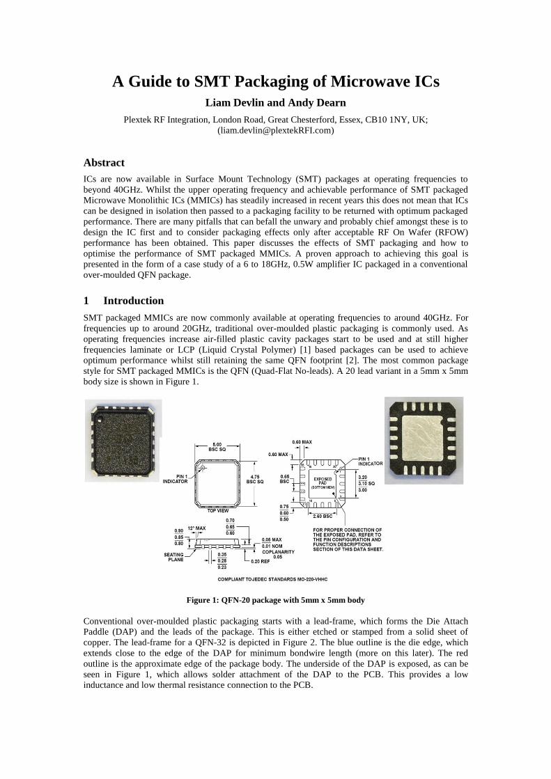
style for SMT packaged MMICs is the QFN (Quad-Flat No-leads). A 20 lead variant in a 5mm x 5mm
body size is shown in Figure 1.
Figure 1: QFN-20 package with 5mm x 5mm body
Conventional over-moulded plastic packaging starts with a lead-frame, which forms the Die Attach
Paddle (DAP) and the leads of the package. This is either etched or stamped from a solid sheet of
copper. The lead-frame for a QFN-32 is depicted in Figure 2. The blue outline is the die edge, which
extends close to the edge of the DAP for minimum bondwire length (more on this later). The red
outline is the approximate edge of the package body. The underside of the DAP is exposed, as can be
seen in Figure 1, which allows solder attachment of the DAP to the PCB. This provides a low
inductance and low thermal resistance connection to the PCB.
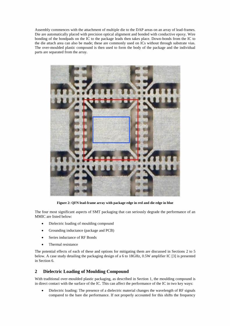
Assembly commences with the attachment of multiple die to the DAP areas on an array of lead-frames.
Die are automatically placed with precision optical alignment and bonded with conductive epoxy. Wire
bonding of the bondpads on the IC to the package leads then takes place. Down-bonds from the IC to
the die attach area can also be made; these are commonly used on ICs without through substrate vias.
The over-moulded plastic compound is then used to form the body of the package and the individual
parts are separated from the array.
Figure 2: QFN lead-frame array with package edge in red and die edge in blue
The four most significant aspects of SMT packaging that can seriously degrade the performance of an
MMIC are listed below:
Dielectric loading of moulding compound
Grounding inductance (package and PCB)
Series inductance of RF Bonds
Thermal resistance
The potential effects of each of these and options for mitigating them are discussed in Sections 2 to 5
below. A case study detailing the packaging design of a 6 to 18GHz, 0.5W amplifier IC [3] is presented
in Section 6.
2 Dielectric Loading of Moulding Compound
With traditional over-moulded plastic packaging, as described in Section 1, the moulding compound is
in direct contact with the surface of the IC. This can affect the performance of the IC in two key ways:
Dielectric loading: The presence of a dielectric material changes the wavelength of RF signals
compared to the bare die performance. If not properly accounted for this shifts the frequency
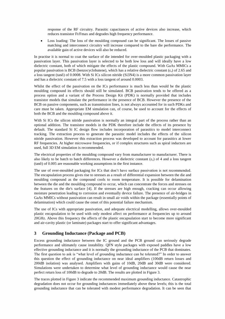
response of the RF circuitry. Parasitic capacitances of active devices also increase, which
reduces transistor Ft/Fmax and degrades high frequency performance.
Loss loading: The loss of the moulding compound can be significant. The losses of passive
matching and interconnect circuitry will increase compared to the bare die performance. The
available gain of active devices will also be reduced.
In practise it is normal to coat the surface of die intended for over-moulded plastic packaging with a
passivation layer. This passivation layer is selected to be both low loss and will ideally have a low
dielectric constant, both of which mitigate the effects of the plastic compound. With GaAs MMICs a
popular passivation is BCB (benzocyclobutene), which has a relative dielectric constant (r) of 2.65 and
a loss tangent (tan) of 0.0008. With Si ICs silicon nitride (Si3N4) is a more common passivation layer
and has a dielectric constant of 7.5 with a loss tangent of around 0.0003.
Whilst the effect of the passivation on the ICs performance is much less than would be the plastic
moulding compound its effects should still be simulated. BCB passivation tends to be offered as a
process option and a variant of the Process Design Kit (PDK) is normally provided that includes
transistor models that simulate the performance in the presence of BCB. However the presence of the
BCB on passive components, such as transmission lines, is not always accounted for in such PDKs and
care must be taken. Appropriate EM simulation can, of course, be used to account for the effects of
both the BCB and the moulding compound above it.
With Si ICs the silicon nitride passivation is normally an integral part of the process rather than an
optional addition. The transistor models in the PDK therefore include the effects of its presence by
default. The standard Si IC design flow includes incorporation of parasitics to model interconnect
tracking. The extraction process to generate the parasitic model includes the effects of the silicon
nitride passivation. However this extraction process was developed to account for parasitics at lower
RF frequencies. At higher microwave frequencies, or if complex structures such as spiral inductors are
used, full 3D EM simulation is recommended.
The electrical properties of the moulding compound vary from manufacturer to manufacturer. There is
also likely to be batch to batch differences. However a dielectric constant (r) of 4 and a loss tangent
(tan) of 0.005 are reasonable working assumptions in the first instance.
The use of over-moulded packaging for ICs that don’t have surface passivation is not recommended.
The encapsulation process gives rise to stresses as a result of differential expansion between the die and
moulding compound as the compound cools to room temperature. It is possible for delamination
between the die and the moulding compound to occur, which can concentrate the forces and stresses on
the features on the die's surface [4]. If the stresses are high enough, cracking can occur allowing
moisture penetration leading to corrosion and eventually device failure. The presence of air-bridges in
GaAs MMICs without passivation can result in small air voids within the package (essentially points of
delamination) which could cause the onset of this potential failure mechanism.
The use of ICs with appropriate passivation, and adequate electrical modelling, allows over-moulded
plastic encapsulation to be used with only modest affect on performance at frequencies up to around
20GHz. Above this frequency the affects of the plastic encapsulation start to become more significant
and air-cavity plastic (or laminate) packages start to offer significant advantages.
3 Grounding Inductance (Package and PCB)
Excess grounding inductance between the IC ground and the PCB ground can seriously degrade
performance and ultimately cause instability. QFN style packages with exposed paddles have a low
effective grounding inductance and it is normally the grounding inductance of the PCB that dominates.
The first question to ask is “what level of grounding inductance can be tolerated?” In order to answer
this question the effect of grounding inductance on near ideal amplifiers (100dB return losses and
200dB isolation) was analysed. Amplifiers with gains of 10dB, 20dB and 30dB were considered.
Simulations were undertaken to determine what level of grounding inductance would cause the near
perfect return loss of 100dB to degrade to 20dB. The results are plotted in Figure 3.
The traces plotted in Figure 3 indicate the recommended maximum grounding inductance. Catastrophic
degradation does not occur for grounding inductances immediately above these levels; this is the total
grounding inductance that can be tolerated with modest performance degradation. It can be seen that
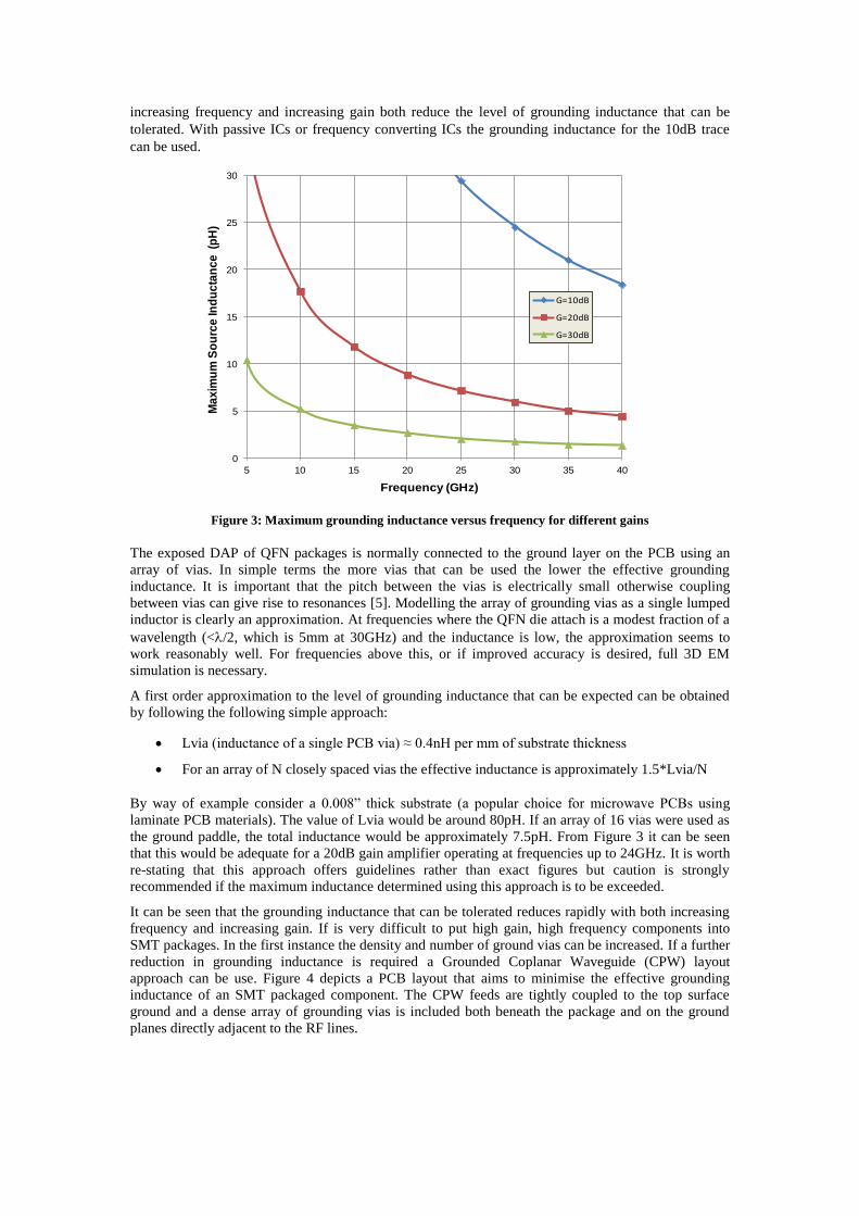
increasing frequency and increasing gain both reduce the level of grounding inductance that can be
tolerated. With passive ICs or frequency converting ICs the grounding inductance for the 10dB trace
can be used.
Figure 3: Maximum grounding inductance versus frequency for different gains
The exposed DAP of QFN packages is normally connected to the ground layer on the PCB using an
array of vias. In simple terms the more vias that can be used the lower the effective grounding
inductance. It is important that the pitch between the vias is electrically small otherwise coupling
between vias can give rise to resonances [5]. Modelling the array of grounding vias as a single lumped
inductor is clearly an approximation. At frequencies where the QFN die attach is a modest fraction of a
wavelength (</2, which is 5mm at 30GHz) and the inductance is low, the approximation seems to
work reasonably well. For frequencies above this, or if improved accuracy is desired, full 3D EM
simulation is necessary.
A first order approximation to the level of grounding inductance that can be expected can be obtained
by following the following simple approach:
Lvia (inductance of a single PCB via) ≈ 0.4nH per mm of substrate thickness
For an array of N closely spaced vias the effective inductance is approximately 1.5*Lvia/N
By way of example consider a 0.008” thick substrate (a popular choice for microwave PCBs using
laminate PCB materials). The value of Lvia would be around 80pH. If an array of 16 vias were used as
the ground paddle, the total inductance would be approximately 7.5pH. From Figure 3 it can be seen
that this would be adequate for a 20dB gain amplifier operating at frequencies up to 24GHz. It is worth
re-stating that this approach offers guidelines rather than exact figures but caution is strongly
recommended if the maximum inductance determined using this approach is to be exceeded.
It can be seen that the grounding inductance that can be tolerated reduces rapidly with both increasing
frequency and increasing gain. If is very difficult to put high gain, high frequency components into
SMT packages. In the first instance the density and number of ground vias can be increased. If a further
reduction in grounding inductance is required a Grounded Coplanar Waveguide (CPW) layout
approach can be use. Figure 4 depicts a PCB layout that aims to minimise the effective grounding
inductance of an SMT packaged component. The CPW feeds are tightly coupled to the top surface
ground and a dense array of grounding vias is included both beneath the package and on the ground
planes directly adjacent to the RF lines.
0
5
10
15
20
25
30
5 10 15 20 25 30 35 40
Ma
xim
um
So
urc
e In
du
cta
nc
e (
pH
)
Frequency (GHz)
G=10dB
G=20dB
G=30dB
Figure 4: PCB layout for minimising effective grounding inductance
An alternative option to reducing the grounding inductance to very low levels is to use differential
circuitry. Differential signals do not suffer from the effects of grounding inductance. A differential
signal exists between two package pins (or two PCB routing tracks) and is not referenced to a PCB
ground in the same way as single-ended signals on microstrip of CPW transmission lines. The
differential impedance of the routing tacks needs to be controlled and is influenced by the presence and
proximity of the ground plane but the tolerance to package grounding inductance offers an alternative
approach to pushing up the operating frequency of SMT packaged components. It is an approach
favoured by Si IC designers as most Si processes do not offer low inductance through substrate
grounding vias making the realisation of single-ended circuitry operating at microwave and mm-wave
frequencies extremely difficult.
4 Series Inductance of RF Bonds
The bondwire connections to the RF ports of an IC present a series inductance that can cause serious
performance degradation. Whilst it is possible to compensate for some level of series inductance, the
level (value) of inductance that can be compensated decreases with increasing operating frequency. In
the first instance it is better to consider how the series inductance can be minimised. The options for
this are listed below:
Layout the IC to fit the selected Die Attach Paddle (DAP) with the edge of the die (and so the
RF bond pads) as close to the edge of the DAP as assembly rules allow.
Align the RF pads with the appropriate package lead.
Use multiple bondwires in parallel. An adequately large pad on the IC is required to allow
this.
Use reverse bonding; this simply means bonding to the package first and the die second. After
the placement of the first bond the bonding tool has to move vertically. If the first bond is to
the package some vertical movement is required as the surface of the die is higher than the
surface of the lead-frame. If the first bond is to the die, the bonding tool still moves vertically
in the first instance but now adds unnecessary bondwire length and so inductance.
Consider the use of a custom leadframe. This can allow reductions in the distance between the
DAP and the package lead and so reduce series bondwire length.
Work with the assembly house on the assembly rules that limit the minimum achievable
bondwire length. These limits are in place for good reasons but can sometimes be tightened to
allow small reductions in the minimum bondwire length.
Using the approaches described above the bondwire lengths can be kept short enough to allow
operation to around 40GHz. The use of SMT packages can be pushed a little higher than this by the use
of laminate or LCP based QFN packages [2].
When considering the series inductance that may be expected from a package wire bond in isolation,
the possibility of SMT packaging at frequencies above 20GHz seems impractical. Consider three
parallel bondwires each 1mm long. The overall series inductance would be in the region of 0.4nH.
Figure 5 shows the simulated insertion loss and input match of a series 0.4nH inductor versus
frequency. It can be seen that the return loss drops below 10dB at around 13GHz and the insertion loss
(due entirely to reflection as this is a lossless inductor) reaches 1dB at just above 20GHz.
Figure 5: Simulated s-parameters of a 0.4nH series inductor
Fortunately other practical parasitics of the bond interface can be used to advantage in improving the
RF performance of the bond transition. There will always be some shunt inductance present at each end
of the series bondwire. At the die end this is primarily due to the bondpad, at the PCB end it is
primarily due to the SMT pad for the package lead. Together with the series inductance of the bond
connection, these capacitances form a low pass filter. The RF performance of this low pass filter is
normally superior to that of the inductor alone. The bold traces in Figure 6 show the effect of adding
typical parasitic capacitances to each end of the 0.4nH series bond inductance: A bondpad of 100µm x
80µm on a 100µm thick GaAs die has been assumed, which is large enough to allow attachment of 3
wire bonds. At the PCB end an SMT pad on a Roger 4003 substrate of 0.02” thickness has been
assumed. It can be seen that the return loss now drops below 10dB at around 21GHz rather than 13GHz
and the insertion loss at 20GHz is around 0.4dB, rather than 1dB.
Figure 6: The effect of adding bondpad and PCB capacitance to each side of the 0.4nH inductor
Optimising the RF performance of a bond transition is essentially an exercise in optimising the
capacitances at each end of the bondwires. Figure 7 shows the simulated performance of a 0.4nH series
inductor with shunt capacitors of optimum value for broadband performance at each end. It can be seen
that very good RF performance (return loss> 18dB and insertion loss < 0.1dB) is now obtained to
20GHz.
Figure 7: S-parameters of a 0.4nH bondwire with optimum capacitances at each end
It is not, however, possible to optimise the capacitance values to allow the 0.4nH inductor to have good
broadband performance to 40GHz. The transition is a low-pass filter and the value of the series
inductance limits the upper cut-off frequency. Figure 8 is a plot of the maximum series inductance that
can be compensated in a low pass filter, versus RF frequency. It can be seen that for the 0.4nH series
inductance in the example above, the maximum frequency is 22GHz. This frequency can be pushed a
little if some performance degradation can be tolerated but it is not possible to implement a good
broadband package transition if the series inductance exceeds the value determined from Figure 8. If
the series inductance is found to be higher, then some means of reducing it must be identified. As SMT
packaging is pushed to even higher frequencies some form of Chip Scale Packaging that allows
bondwires to be dispensed with altogether will become necessary [6].
Figure 8: Maximum series inductance versus RF frequency for broadband package transitions
As previously mentioned a custom lead-frame can be used to allow reduced bondwire inductance. It is
also possible to use the lead-frame design to assist in optimising the capacitive parts of the transition. A
photograph of a custom lead-frame that has been optimised for mm-wave performance is shown in
Figure 9. This example is from Endwave and the RF transitions are provided at the centre of all four
sides. It can be seen that the gap between the RF lead and the DAP is smaller than all other gaps, so
allowing the bondwire length and inductance to be reduced. A wide end to the RF lead has been
implemented to optimise the shunt capacitance. This must be undertaken with a specific PCB substrate
in mind. It can also be seen that the leads either side of the signal lead are connected directly to the
DAP. The intention is that these are ground contacts allowing the package to be used with a GCPWG
interface. As previously mentioned the GCPWG interface can be used to reduce the effective
grounding inductance of the package. It can also provide increased screening between RF routing
tracks on the PCB.
Figure 9: Example of a custom lead-frame optimised for RF performance
The guidelines above explain the issues with bondwire parasitic and the approach for compensation. In
practise optimisation of the RF performance of a package transition is most conveniently undertaken
with the aid of 3D EM simulation of the transition. A proven approach to this optimisation process is
included in the case study presented later in this paper (Section 6).
Maximum Perfectly Compensatable Series Inductance Versus
Frequency
0
0.2
0.4
0.6
0.8
1
0 5 10 15 20 25 30 35 40 45 50
Frequency (GHz)
Ind
ucta
nce (
nH
)
5 Thermal Resistance
It is important that ICs operate with acceptable (adequately low) junction temperatures. In simple
terms, the higher junction temperature the lower the median life-time of the device. The thermal
resistance of the package, and the die attach material, add to the thermal resistance of the IC so
increasing the junction temperature for a given power dissipation and ambient temperature. A full
treatment of thermal issues of ICs and packaging is beyond the scope of this paper but a useful
summary can be found in [7].
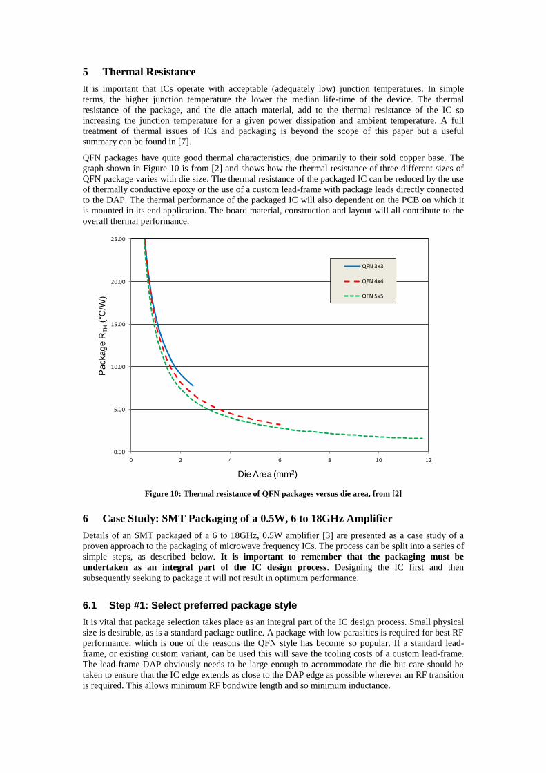
QFN packages have quite good thermal characteristics, due primarily to their sold copper base. The
graph shown in Figure 10 is from [2] and shows how the thermal resistance of three different sizes of
QFN package varies with die size. The thermal resistance of the packaged IC can be reduced by the use
of thermally conductive epoxy or the use of a custom lead-frame with package leads directly connected
to the DAP. The thermal performance of the packaged IC will also dependent on the PCB on which it
is mounted in its end application. The board material, construction and layout will all contribute to the
overall thermal performance.
Figure 10: Thermal resistance of QFN packages versus die area, from [2]
6 Case Study: SMT Packaging of a 0.5W, 6 to 18GHz Amplifier
Details of an SMT packaged of a 6 to 18GHz, 0.5W amplifier [3] are presented as a case study of a
proven approach to the packaging of microwave frequency ICs. The process can be split into a series of
simple steps, as described below. It is important to remember that the packaging must be
undertaken as an integral part of the IC design process. Designing the IC first and then
subsequently seeking to package it will not result in optimum performance.
6.1 Step #1: Select preferred package style
It is vital that package selection takes place as an integral part of the IC design process. Small physical
size is desirable, as is a standard package outline. A package with low parasitics is required for best RF
performance, which is one of the reasons the QFN style has become so popular. If a standard lead-
frame, or existing custom variant, can be used this will save the tooling costs of a custom lead-frame.
The lead-frame DAP obviously needs to be large enough to accommodate the die but care should be
taken to ensure that the IC edge extends as close to the DAP edge as possible wherever an RF transition
is required. This allows minimum RF bondwire length and so minimum inductance.
0.00
5.00
10.00
15.00
20.00
25.00
0 2 4 6 8 10 12
Packag
e R
TH
( C
/W)
Die Area (mm2)
QFN 3x3
QFN 4x4
QFN 5x5
For the amplifier in this case study the standard QFN-20 CSP with 5mm x 5mm body and exposed
paddle (shown in Figure 1) was selected.
6.2 Step #2: Select PCB material
The parasitics associated with the PCB can strongly affect the performance of the packaged part. In
particular the grounding inductance can significantly modify the performance and in the worst case can
cause instability. The parasitics of the SMT pad will also affect the performance of the RF transition
and must be considered.
In order to ensure that the grounding inductance is adequately low, the substrate height must be
selected with care and the number of vias used to ground the exposed DAP must be adequate.
Guidelines for estimating the grounding inductance are presented in Section 3. Material cost is another
important criterion and is one of the reasons that laminate based materials have become so popular for
microwave frequency PCBs. Dielectric constant must also be considered. Low dielectric constant
reduces the parasitic capacitance of the SMT pads and allows lower loss routing tracks for a given
substrate height. These reasons were used to select Rogers 4003 with a substrate height of 0.008” for
the IC under consideration.
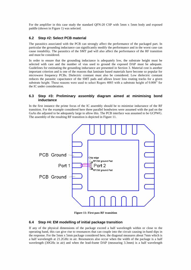
6.3 Step #3: Preliminary assembly diagram aimed at minimising bond inductance
In the first instance the prime focus of the IC assembly should be to minimise inductance of the RF
transition. For the example considered here three parallel bondwires were assumed with the pad on the
GaAs die adjusted to be adequately large to allow this. The PCB interface was assumed to be GCPWG.
The assembly of the resulting RF transition is depicted in Figure 11.
Figure 11: First pass RF transition
6.4 Step #4: EM modelling of initial package transition
If any of the physical dimensions of the package exceed a half wavelength within or close to the
operating band, this can give rise to resonances that can couple into the circuit causing in-band dips in
the response. For the 5mm x 5mm package considered here, the diagonal measures about 7mm which is
a half wavelength at 21.2GHz in air. Resonances also occur when the width of the package is a half
wavelength (30GHz in air) and when the lead-frame DAP (measuring 3.3mm) is a half wavelength
(45.5GHz in air). The presence of the dielectric will serve to reduce the frequency of these resonances.
The resonant frequencies will also be modified by the PCB on to which the package is assembled. If
any of the multiple resonances of the package falls within band they can couple into the circuit causing
dips in the response.
EM simulation of the complete package can predict these resonances. It is also possible to push in-band
resonances out of band by the use of a modified (custom) lead-frame. This is explained in more detail
and demonstrated by measurement in [8]. If the package does not have in-band resonances due to its
physical size the transition can be modelled in isolation, without modelling the entire package. This
greatly simplifies the modelling exercise and is the approach taken here.
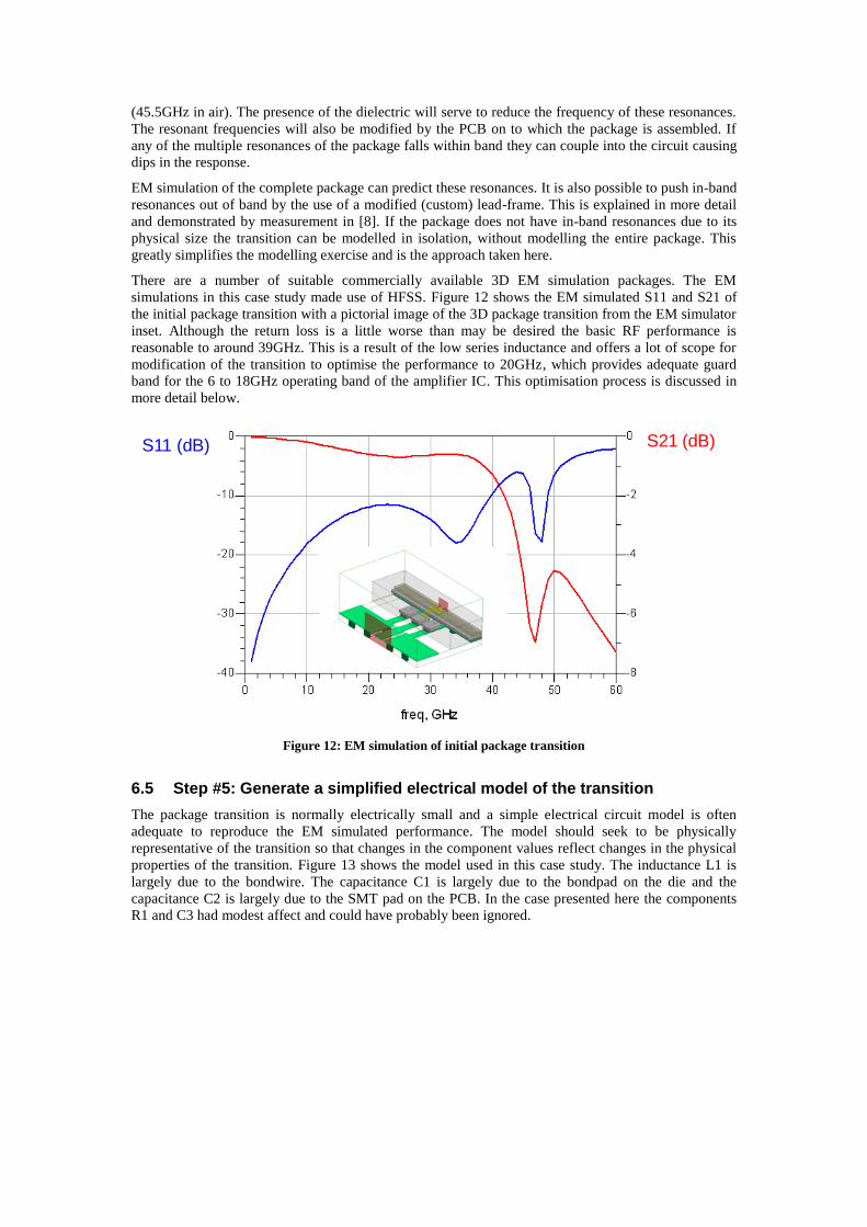
There are a number of suitable commercially available 3D EM simulation packages. The EM
simulations in this case study made use of HFSS. Figure 12 shows the EM simulated S11 and S21 of
the initial package transition with a pictorial image of the 3D package transition from the EM simulator
inset. Although the return loss is a little worse than may be desired the basic RF performance is
reasonable to around 39GHz. This is a result of the low series inductance and offers a lot of scope for
modification of the transition to optimise the performance to 20GHz, which provides adequate guard
band for the 6 to 18GHz operating band of the amplifier IC. This optimisation process is discussed in
more detail below.
Figure 12: EM simulation of initial package transition
6.5 Step #5: Generate a simplified electrical model of the transition
The package transition is normally electrically small and a simple electrical circuit model is often
adequate to reproduce the EM simulated performance. The model should seek to be physically
representative of the transition so that changes in the component values reflect changes in the physical
properties of the transition. Figure 13 shows the model used in this case study. The inductance L1 is
largely due to the bondwire. The capacitance C1 is largely due to the bondpad on the die and the
capacitance C2 is largely due to the SMT pad on the PCB. In the case presented here the components
R1 and C3 had modest affect and could have probably been ignored.
S11 (dB) S21 (dB)
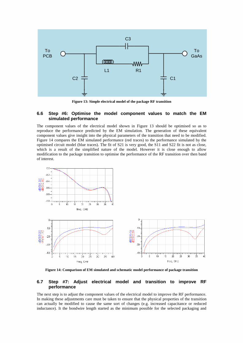
Figure 13: Simple electrical model of the package RF transition
6.6 Step #6: Optimise the model component values to match the EM simulated performance
The component values of the electrical model shown in Figure 13 should be optimised so as to
reproduce the performance predicted by the EM simulation. The generation of these equivalent
component values give insight into the physical parameters of the transition that need to be modified.
Figure 14 compares the EM simulated performance (red traces) to the performance simulated by the
optimised circuit model (blue traces). The fit of S21 is very good, the S11 and S22 fit is not as close,
which is a result of the simplified nature of the model. However it is close enough to allow
modification to the package transition to optimise the performance of the RF transition over then band
of interest.
Figure 14: Comparison of EM simulated and schematic model performance of package transition
6.7 Step #7: Adjust electrical model and transition to improve RF performance
The next step is to adjust the component values of the electrical model to improve the RF performance.
In making these adjustments care must be taken to ensure that the physical properties of the transition
can actually be modified to cause the same sort of changes (e.g. increased capacitance or reduced
inductance). It the bondwire length started as the minimum possible for the selected packaging and
C1C2
C3
L1 R1
To
GaAs
To
PCB
assembly technology there is little point in reducing the series inductance of the model (L1) to obtain
improved performance. In the case considered here the following component changes were found to
allow improved RF performance over the band of interest and were physically practical:
The inductance L1 was increased (easily facilitated by a shift from 3 parallel bondwires to 2)
The capacitance C1 was reduced (facilitated by reducing the size of the bondpad on the GaAs
die)
The capacitance C2 was reduced (implemented by increasing the gaps from the RF SMT pad
to the adjacent grounds)
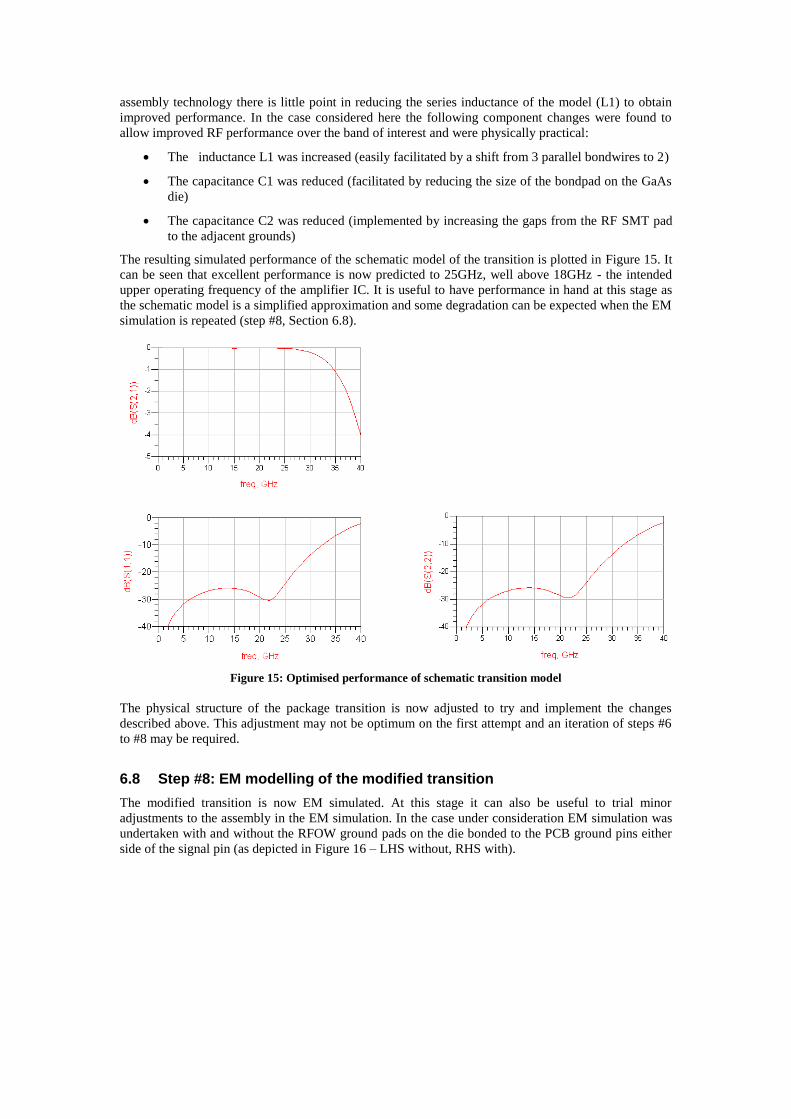
The resulting simulated performance of the schematic model of the transition is plotted in Figure 15. It
can be seen that excellent performance is now predicted to 25GHz, well above 18GHz - the intended
upper operating frequency of the amplifier IC. It is useful to have performance in hand at this stage as
the schematic model is a simplified approximation and some degradation can be expected when the EM
simulation is repeated (step #8, Section 6.8).
Figure 15: Optimised performance of schematic transition model
The physical structure of the package transition is now adjusted to try and implement the changes
described above. This adjustment may not be optimum on the first attempt and an iteration of steps #6
to #8 may be required.
6.8 Step #8: EM modelling of the modified transition
The modified transition is now EM simulated. At this stage it can also be useful to trial minor
adjustments to the assembly in the EM simulation. In the case under consideration EM simulation was
undertaken with and without the RFOW ground pads on the die bonded to the PCB ground pins either
side of the signal pin (as depicted in Figure 16 – LHS without, RHS with).
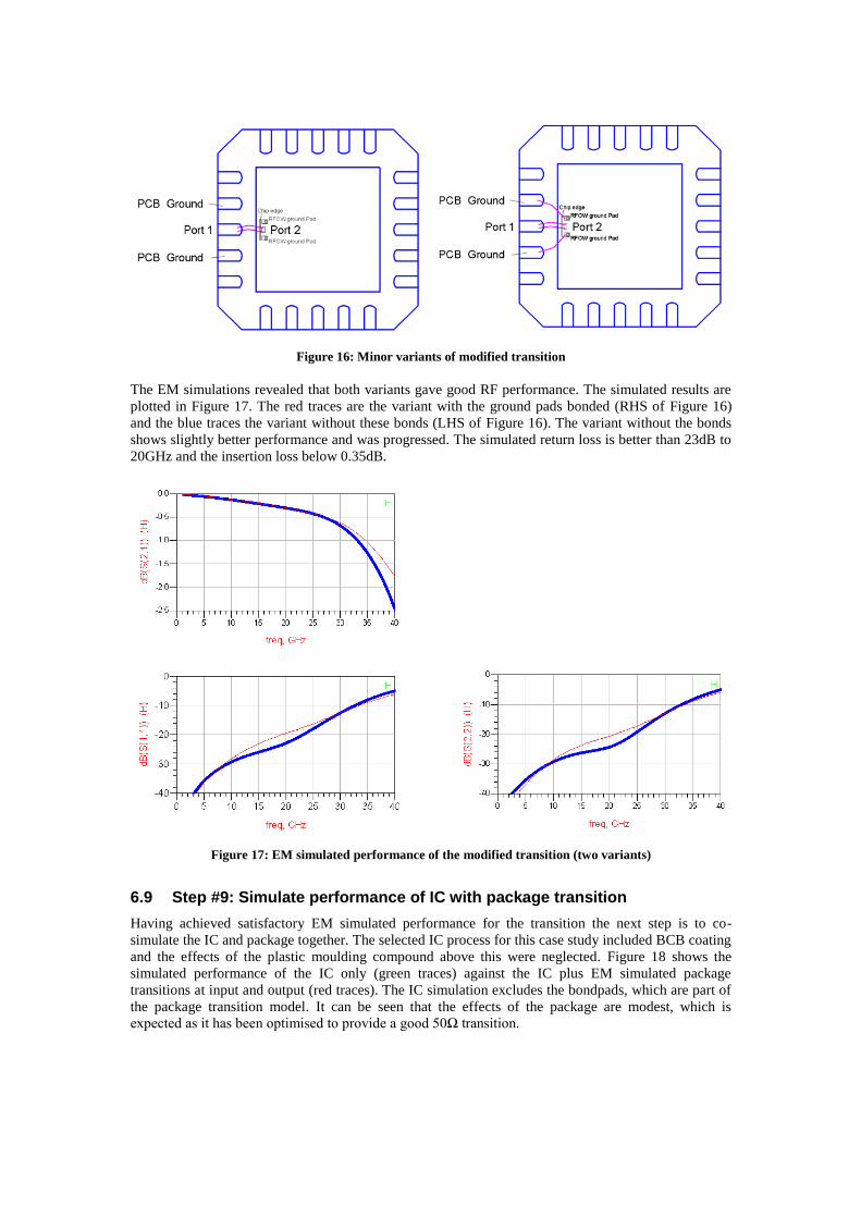
Figure 16: Minor variants of modified transition
The EM simulations revealed that both variants gave good RF performance. The simulated results are
plotted in Figure 17. The red traces are the variant with the ground pads bonded (RHS of Figure 16)
and the blue traces the variant without these bonds (LHS of Figure 16). The variant without the bonds
shows slightly better performance and was progressed. The simulated return loss is better than 23dB to
20GHz and the insertion loss below 0.35dB.
Figure 17: EM simulated performance of the modified transition (two variants)
6.9 Step #9: Simulate performance of IC with package transition
Having achieved satisfactory EM simulated performance for the transition the next step is to co-
simulate the IC and package together. The selected IC process for this case study included BCB coating
and the effects of the plastic moulding compound above this were neglected. Figure 18 shows the
simulated performance of the IC only (green traces) against the IC plus EM simulated package
transitions at input and output (red traces). The IC simulation excludes the bondpads, which are part of
the package transition model. It can be seen that the effects of the package are modest, which is
expected as it has been optimised to provide a good 50Ω transition.
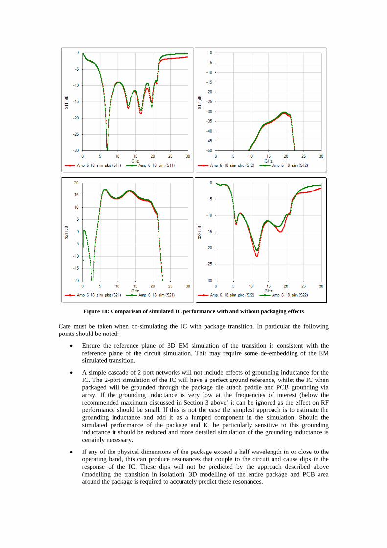
Figure 18: Comparison of simulated IC performance with and without packaging effects
Care must be taken when co-simulating the IC with package transition. In particular the following
points should be noted:
Ensure the reference plane of 3D EM simulation of the transition is consistent with the
reference plane of the circuit simulation. This may require some de-embedding of the EM
simulated transition.
A simple cascade of 2-port networks will not include effects of grounding inductance for the
IC. The 2-port simulation of the IC will have a perfect ground reference, whilst the IC when
packaged will be grounded through the package die attach paddle and PCB grounding via
array. If the grounding inductance is very low at the frequencies of interest (below the
recommended maximum discussed in Section 3 above) it can be ignored as the effect on RF
performance should be small. If this is not the case the simplest approach is to estimate the
grounding inductance and add it as a lumped component in the simulation. Should the
simulated performance of the package and IC be particularly sensitive to this grounding
inductance it should be reduced and more detailed simulation of the grounding inductance is
certainly necessary.
If any of the physical dimensions of the package exceed a half wavelength in or close to the
operating band, this can produce resonances that couple to the circuit and cause dips in the
response of the IC. These dips will not be predicted by the approach described above
(modelling the transition in isolation). 3D modelling of the entire package and PCB area
around the package is required to accurately predict these resonances.
6.10 Step #10 Assemble ICs into packages and evaluate
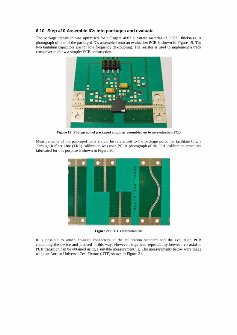
The package transition was optimised for a Rogers 4003 substrate material of 0.008” thickness. A
photograph of one of the packaged ICs assembled onto an evaluation PCB is shown in Figure 19. The
two tantalum capacitors are for low frequency de-coupling. The resistor is used to implement a track
cross-over to allow a simpler PCB construction.
Figure 19: Photograph of packaged amplifier assembled on to an evaluation PCB
Measurements of the packaged parts should be referenced to the package ports. To facilitate this, a
Through Reflect Line (TRL) calibration was used [9]. A photograph of the TRL calibration structures
fabricated for this purpose is shown in Figure 20.
Figure 20: TRL calibration tile
It is possible to attach co-axial connectors to the calibration standard and the evaluation PCB
containing the device and proceed in this way. However, improved repeatability between co-axial to
PCB transition can be obtained using a suitable measurement jig. The measurements below were made
using an Anritsu Universal Test Fixture (UTF) shown in Figure 21.
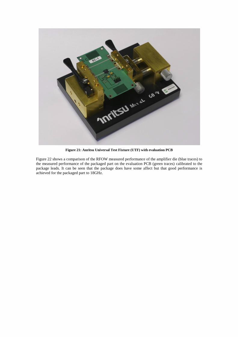
Figure 21: Anritsu Universal Test Fixture (UTF) with evaluation PCB
Figure 22 shows a comparison of the RFOW measured performance of the amplifier die (blue traces) to
the measured performance of the packaged part on the evaluation PCB (green traces) calibrated to the
package leads. It can be seen that the package does have some affect but that good performance is
achieved for the packaged part to 18GHz.
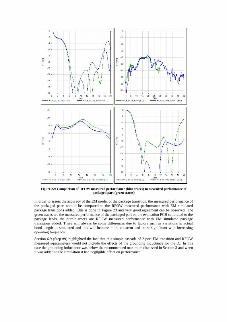
Figure 22: Comparison of RFOW measured performance (blue traces) to measured performance of packaged part (green traces)
In order to assess the accuracy of the EM model of the package transition, the measured performance of
the packaged parts should be compared to the RFOW measured performance with EM simulated
package transitions added. This is done in Figure 23 and very good agreement can be observed. The
green traces are the measured performance of the packaged part on the evaluation PCB calibrated to the
package leads; the purple traces are RFOW measured performance with EM simulated package
transitions added. There will always be some differences due to factors such as variations in actual
bond length to simulated and this will become more apparent and more significant with increasing
operating frequency.
Section 6.9 (Step #9) highlighted the fact that this simple cascade of 2-port EM transition and RFOW
measured s-parameters would not include the effects of the grounding inductance for the IC. In this
case the grounding inductance was below the recommended maximum discussed in Section 3 and when
it was added to the simulation it had negligible effect on performance.
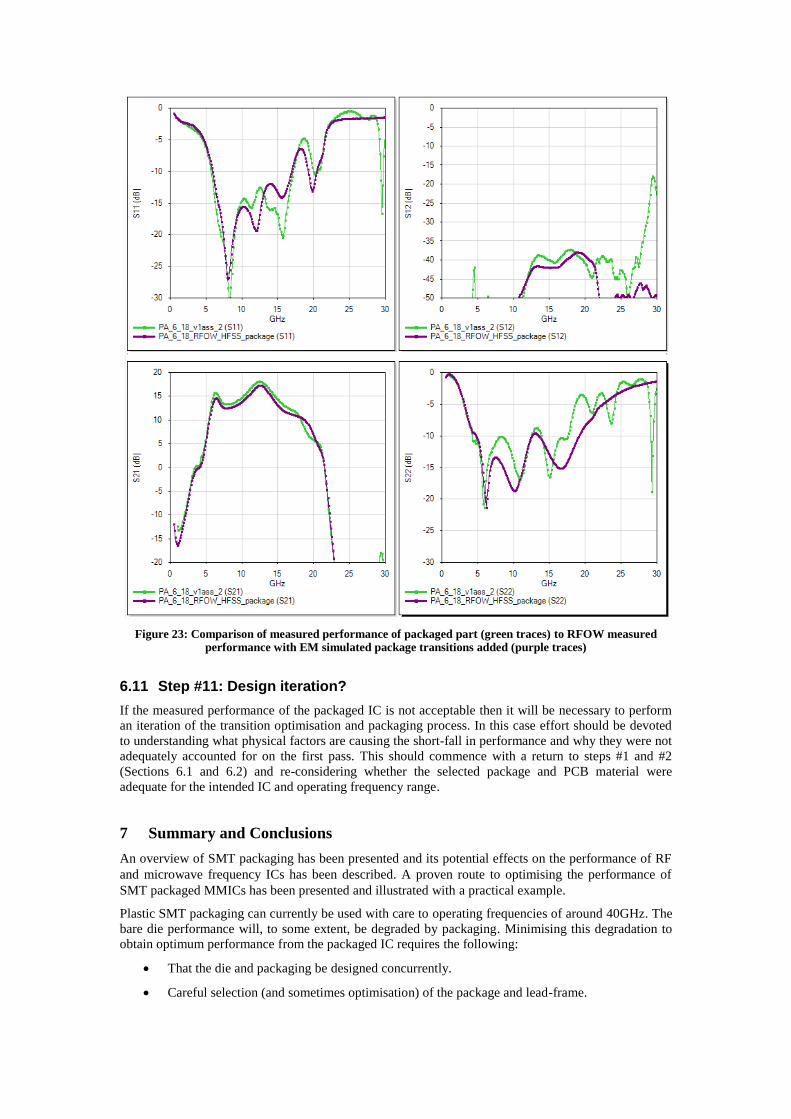
Figure 23: Comparison of measured performance of packaged part (green traces) to RFOW measured performance with EM simulated package transitions added (purple traces)
6.11 Step #11: Design iteration?
If the measured performance of the packaged IC is not acceptable then it will be necessary to perform
an iteration of the transition optimisation and packaging process. In this case effort should be devoted
to understanding what physical factors are causing the short-fall in performance and why they were not
adequately accounted for on the first pass. This should commence with a return to steps #1 and #2
(Sections 6.1 and 6.2) and re-considering whether the selected package and PCB material were
adequate for the intended IC and operating frequency range.
7 Summary and Conclusions
An overview of SMT packaging has been presented and its potential effects on the performance of RF
and microwave frequency ICs has been described. A proven route to optimising the performance of
SMT packaged MMICs has been presented and illustrated with a practical example.
Plastic SMT packaging can currently be used with care to operating frequencies of around 40GHz. The
bare die performance will, to some extent, be degraded by packaging. Minimising this degradation to
obtain optimum performance from the packaged IC requires the following:
That the die and packaging be designed concurrently.
Careful selection (and sometimes optimisation) of the package and lead-frame.
Detailed design, EM simulation and optimisation of the package transition, from RF bondpad
on the die to RF tracks on the PCB
Appropriate selection of the PCB material and optimisation of the layout for package
attachment, including the grounding pattern.
In the event that any of the physical dimensions of the package exceed a half wavelength in or
close to the operating band, 3D modelling of the entire package and PCB area around the
package is required to accurately predict these resonances. A custom lead-frame can be
produced to shift such resonances out of band.
8 References
[1] Melvin, S., “Custom MMIC Packaging Solutions for High Frequency Thermally Efficient
Surface Mount Applications”, proceedings of the RF and Microwave Society (ARMMS)
Conference, April, 2011
[2] Evans, P.W. and Fattorini, T., “Electrical, Thermal, Reliability and Cost Considerations for
Millimeter-Wave Surface Mount Packages”, CS MANTECH Conference, April 23rd - 26th,
201c
[3] Stuart Glynn and Liam Devlin, “A Low Cost, Plastic Packaged, 0.5W, 6-18GHz Amplifier
MMIC”, proceedings of the RF and Microwave Society (ARMMS) Conference, November
21st and 22nd, 2011
[4] Sauber, J, “Modeling of Die Surface Features on Integrated Circuits to Improve Device
Reliability”, http://www.mscsoftware.com/support/library/conf/wuc96/02_saub.cfm
[5] Tischler, T., Rudolph, M., Kilk, A. and Heinrich, W. “Via Arrays for Grounding in Multilayer
Packaging - Frequency Limits and Design Rules”, IEEE MTT-S, 2003, vol. 2, pp. 1147- 1150
[6] Knapp, H., Treml M. et al, “Three-channel 77 GHz automotive radar transmitter in plastic
package”, proceedings of the Radio Frequency Integrated Circuits (RFIC) Symposium, June
2012, pp. 119 - 122
[7] UMS Application Note AN0018, “THERMAL MANAGEMENT for DIES and PLASTIC
PACKAGES”,
http://www.ums-gaas.com/telechargement/AN0018_9084_Thermal_Management_for_Dies_and_Packages_1.pdf
[8] A. Bessemoulin, P. Evans, A. Fattorini, “A 5-45 GHz Linear Voltage Controlled Attenuator
MMIC in 3×3-mm Plastic Package”, 2012 European Microwave Integrated Circuit
Conference (EuMIC)
[9] Applying the 8510 TRL Calibration for Non-Coaxial Measurements, Agilent Product Note
8510-8A; http://cp.literature.agilent.com/litweb/pdf/5091-3645E.pdf