Embed Size (px)
Citation preview
Sampling SAR ADC Oversampling
Delta-Sigma ADC
Single
sample per
conversion
Multiple samples,
averaged
Signal Noise
1 2 3 4Data
Out
Pipeline ADC
1 2 3 4Data
Out1 2 3 4
Data
Out
1
2
1
2
Application ReportSBAA147B–August 2006–Revised October 2011
A Glossary of Analog-to-Digital Specifications andPerformance Characteristics
Bonnie Baker ................................................................................................ Data Acquisition Products
ABSTRACT
This glossary is a collection of the definitions of Texas Instruments' Delta-Sigma (ΔΣ), successiveapproximation register (SAR), and pipeline analog-to-digital (A/D) Converter specifications andperformance characteristics. Although there is a considerable amount of detail in this document, theproduct data sheet for a particular product specification is the best and final reference. To download orview a specific data converter product data sheet, see the Texas Instruments web site at www.ti.com/.
Glossary of Terms
Acquisition Time:
Refer to Figure 1 when comparing SAR, Pipeline, and Delta-Sigma converter acquisition time.
Figure 1. SAR vs Pipeline vs ΔΣ A/D Converters Sampling Algorithms Comparison
• Acquisition time, Delta-Sigma A/D Converters–The Delta-Sigma (ΔΣ) converter averages multiple samples for each conversion result. The averagingperformed by the converter usually occurs in the form of a Finite Impulse Response (FIR) or InfiniteImpulse Response (IIR) digital filter. Consequently, the acquisition time is longer than it is with a SARor pipeline converter, which only samples the signal once for each conversion. Figure 1 illustrates oneof the differences between the sampling mechanism of a SAR, a Pipeline and a ΔΣ converter. If the
I2C is a trademark of Koninklijke Philips Electronics N.V.SPI is a trademark of Motorola, Inc.All other trademarks are the property of their respective owners.
1SBAA147B–August 2006–Revised October 2011 A Glossary of Analog-to-Digital Specifications and Performance CharacteristicsSubmit Documentation Feedback
Copyright © 2006–2011, Texas Instruments Incorporated
Hold Sample Hold
Acquisition time
or sample time
Aperture time
Sample Error
(offset, nonlinearity)Input signal
1 2 3 4 5 6 7 8 9 10 11 12 13 14
D
9
D
10
D
8
D
7
D
6
D
5
D
4
D
3
D
2
D
1
D
0
D
11
CS
CLK
DOUT
Null Bit
All data transitions occur
on the falling edge of SLK
Sample
Period Conversion Period
15
Clock #15 is
optional;
D0 is clocked out
on falling edge of
Clock #14
A
B
www.ti.com
user presents a step-input to the delta-sigma converter input or switches a multiplexer output channel,the converter will require time for the digital filter to refresh with the new signal. If a snap-shot of thesignal or a defined acquisition point in time is required, it is more appropriate to use a SAR A/Dconverter.
• Acquisition time, Pipeline A/D Converters–With a pipeline A/D converter, the user initiates the conversion process with the rising edge (or fallingedge, as specified in the product data sheet) of the external input clock. The capture of the differentialinput signal follows the opening of the input internal switches. See Figure 1 and Figure 2.
Figure 2. Acquisition Time (Sample Time) and Aperture Time
• Acquisition time, SAR A/D Converters–The acquisition time for the SAR converter is the time required for the sampling mechanism to capturethe input voltage. This time begins after the sample command is given where the hold capacitorcharges. Some converters have the capability of sampling the input signal in response to a samplingpin on the converter. Other SAR CMOS converters sample with the clock after CS (chip select) drops(with a serial peripheral interface, or SPI™). Figure 3 shows an example of a clock-initiated sampleusing the ADS7816. Also see Figure 1 and Figure 2.
A Chip select (CS) falls.
B The falling edge of the clock closes the sample switch.
Figure 3. Clock-Initiated Sample for a SAR A/D Converter
Analog Input, Analog Bandwidth: The input frequency where the reconstructed output of the A/Dconverter is 3dB below the value of the input signal.
Analog Input, Capacitance, Common-mode: The common-mode capacitance of an A/D converter is thecapacitance between each analog signal input(s) and ground.
Analog Input, Capacitance, Differential: The capacitance between the positive input (AIN+) and negativeinput (AIN–) of an A/D converter with a differential input.
2 A Glossary of Analog-to-Digital Specifications and Performance Characteristics SBAA147B–August 2006–Revised October 2011Submit Documentation Feedback
Copyright © 2006–2011, Texas Instruments Incorporated
±200mV Maximum
DACADC
AIN+
AIN-
www.ti.com
Analog Input, Differential Input: With the analog differential input, both input pins of the A/D convertercan swing the full range, and typically change in a balanced fashion—that is, as one input goes up, theother goes down in a corresponding way. The differential input offers the advantage of subtracting the twoinputs and provides common-mode rejection. These types of inputs are commonly found in single-supplyconverters, such as delta-sigma or pipeline converters. The differential input offers the advantages ofcommon-mode rejection, with a smaller input voltage swing required on each pin while preserving a highdynamic range.
Analog Input, Impedance, Common-mode: The impedance between each analog signal input of theA/D converter and ground.
Analog Input, Impedance, Differential: The impedance between the positive input (AIN+) and negativeinput (AIN–) of an A/D converter with a differential input.
Analog Input, Voltage Range, Absolute: The absolute analog voltage range of an A/D converter is themaximum and minimum voltage limit of the input stage (compared to ground and/or the analog supplyvoltage). This term describes the absolute input voltage range limits of the input stage. Usually, thepositive and negative power supplies impose these limits on the device, unless there is a resistancenetwork on the input. If there is a resistive input network, the absolute inputs can exceed the positive andnegative power supplies.
Analog Input, Voltage Range, Bipolar Input Mode (Differential Inputs): An A/D converter configured ina Bipolar Input Mode has an input range that uses two input pins and allows negative and positive analoginputs on both pins with respect to each other. In this configuration, neither input pin goes below or abovethe absolute input voltage range. (See Input Voltage Range – Differential Inputs.)
Analog Input, Voltage Range, Full-Scale (FS or FSR): The converter digitizes the input signal up to thefull-scale input voltage. The internal or external applied voltage reference value determines the full-scaleinput voltage range. The actual FS input voltage range will vary from device to device. Refer to thespecific A/D converter data sheet for details.
• For an n -bit converter, FS is equal to:
FS = (2n) × (ideal code width)
• For delta-sigma converters, FSR is often used to express units in terms of percentages. Forinstance, you may find INL defined at ±0.001% of FSR. In this instance, the input range of the A/Dconverter could be ±2.5V, with a FSR = 5V.Also see: Analog Inputs, Differential Inputs. Refer to a specific A/D converter data sheet for details.
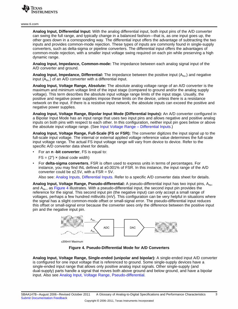
Analog Input, Voltage Range, Pseudo-differential: A pseudo-differential input has two input pins, AIN+
and AIN–, as Figure 4 illustrates. With a pseudo-differential input, the second input pin provides thereference for the signal. This second input pin (the negative input) can only accept a small range ofvoltages, perhaps a few hundred millivolts (mV). This configuration can be very helpful in situations wherethe signal has a slight common-mode offset or small-signal error. The pseudo-differential input reducesthis offset or small-signal error because the converter sees only the difference between the positive inputpin and the negative input pin.
Figure 4. Pseudo-Differential Mode for A/D Converters
Analog Input, Voltage Range, Single-ended (unipolar and bipolar): A single-ended input A/D converteris configured for one input voltage that is referenced to ground. Some single-supply devices have asingle-ended input range that allows only positive analog input signals. Other single-supply (anddual-supply) parts handle a signal that moves both above ground and below ground, and have a bipolarinput. Also see Analog Input, Voltage Range, Pseudo-differential.
3SBAA147B–August 2006–Revised October 2011 A Glossary of Analog-to-Digital Specifications and Performance CharacteristicsSubmit Documentation Feedback
Copyright © 2006–2011, Texas Instruments Incorporated
Full-Scale = (A A ) (A A )( )IN+(MAX) IN (MIN) IN+(MIN) IN (MAX)- - -- -
ADCADC
Input
IN
IN
IN
IN
+ fs + fs/2
+ fs/2- sf
- sf /2
- sf /2
VCM
VCM
VCM
VCM
Single-Ended Input Differential Input
SNR = 20log10( )1
(2 f t )p j
t =j (ta + t )c
2 2
www.ti.com
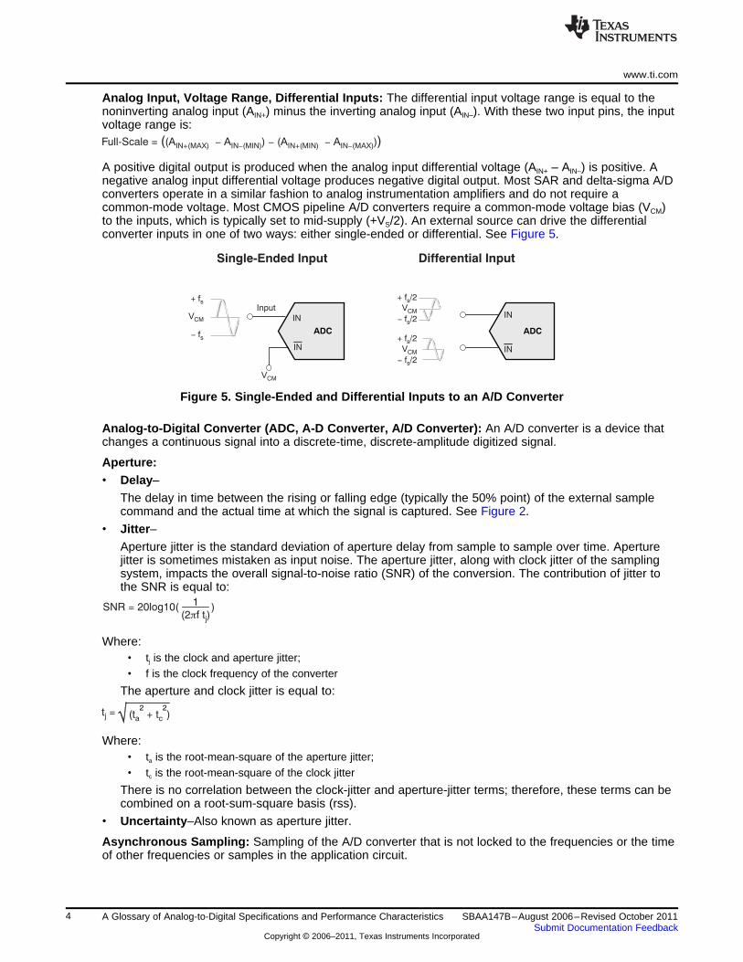
Analog Input, Voltage Range, Differential Inputs: The differential input voltage range is equal to thenoninverting analog input (AIN+) minus the inverting analog input (AIN–). With these two input pins, the inputvoltage range is:
A positive digital output is produced when the analog input differential voltage (AIN+ – AIN–) is positive. Anegative analog input differential voltage produces negative digital output. Most SAR and delta-sigma A/Dconverters operate in a similar fashion to analog instrumentation amplifiers and do not require acommon-mode voltage. Most CMOS pipeline A/D converters require a common-mode voltage bias (VCM)to the inputs, which is typically set to mid-supply (+VS/2). An external source can drive the differentialconverter inputs in one of two ways: either single-ended or differential. See Figure 5.
Figure 5. Single-Ended and Differential Inputs to an A/D Converter
Analog-to-Digital Converter (ADC, A-D Converter, A/D Converter): An A/D converter is a device thatchanges a continuous signal into a discrete-time, discrete-amplitude digitized signal.
Aperture:• Delay–
The delay in time between the rising or falling edge (typically the 50% point) of the external samplecommand and the actual time at which the signal is captured. See Figure 2.
• Jitter–Aperture jitter is the standard deviation of aperture delay from sample to sample over time. Aperturejitter is sometimes mistaken as input noise. The aperture jitter, along with clock jitter of the samplingsystem, impacts the overall signal-to-noise ratio (SNR) of the conversion. The contribution of jitter tothe SNR is equal to:
Where:• tj is the clock and aperture jitter;• f is the clock frequency of the converter
The aperture and clock jitter is equal to:
Where:• ta is the root-mean-square of the aperture jitter;• tc is the root-mean-square of the clock jitter
There is no correlation between the clock-jitter and aperture-jitter terms; therefore, these terms can becombined on a root-sum-square basis (rss).
• Uncertainty–Also known as aperture jitter.
Asynchronous Sampling: Sampling of the A/D converter that is not locked to the frequencies or the timeof other frequencies or samples in the application circuit.
4 A Glossary of Analog-to-Digital Specifications and Performance Characteristics SBAA147B–August 2006–Revised October 2011Submit Documentation Feedback
Copyright © 2006–2011, Texas Instruments Incorporated
www.ti.com
Average Noise Floor: In a Fast Fourier Transform (FFT) representation of converter data, the averagenoise floor is a calculated average of all of the bins within the FFT plot, excluding the input signal andsignal harmonics.
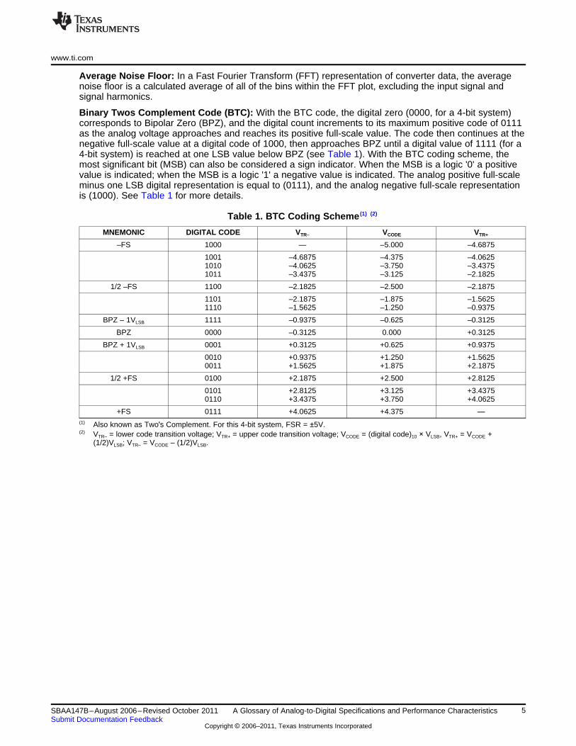
Binary Twos Complement Code (BTC): With the BTC code, the digital zero (0000, for a 4-bit system)corresponds to Bipolar Zero (BPZ), and the digital count increments to its maximum positive code of 0111as the analog voltage approaches and reaches its positive full-scale value. The code then continues at thenegative full-scale value at a digital code of 1000, then approaches BPZ until a digital value of 1111 (for a4-bit system) is reached at one LSB value below BPZ (see Table 1). With the BTC coding scheme, themost significant bit (MSB) can also be considered a sign indicator. When the MSB is a logic '0' a positivevalue is indicated; when the MSB is a logic '1' a negative value is indicated. The analog positive full-scaleminus one LSB digital representation is equal to (0111), and the analog negative full-scale representationis (1000). See Table 1 for more details.
Table 1. BTC Coding Scheme (1) (2)
MNEMONIC DIGITAL CODE VTR– VCODE VTR+
–FS 1000 — –5.000 –4.6875
1001 –4.6875 –4.375 –4.06251010 –4.0625 –3.750 –3.43751011 –3.4375 –3.125 –2.1825
1/2 –FS 1100 –2.1825 –2.500 –2.1875
1101 –2.1875 –1.875 –1.56251110 –1.5625 –1.250 –0.9375
BPZ – 1VLSB 1111 –0.9375 –0.625 –0.3125
BPZ 0000 –0.3125 0.000 +0.3125
BPZ + 1VLSB 0001 +0.3125 +0.625 +0.9375
0010 +0.9375 +1.250 +1.56250011 +1.5625 +1.875 +2.1875
1/2 +FS 0100 +2.1875 +2.500 +2.8125
0101 +2.8125 +3.125 +3.43750110 +3.4375 +3.750 +4.0625
+FS 0111 +4.0625 +4.375 —(1) Also known as Two's Complement. For this 4-bit system, FSR = ±5V.(2) VTR– = lower code transition voltage; VTR+ = upper code transition voltage; VCODE = (digital code)10 × VLSB, VTR+ = VCODE +
(1/2)VLSB; VTR– = VCODE – (1/2)VLSB.
5SBAA147B–August 2006–Revised October 2011 A Glossary of Analog-to-Digital Specifications and Performance CharacteristicsSubmit Documentation Feedback
Copyright © 2006–2011, Texas Instruments Incorporated
www.ti.com
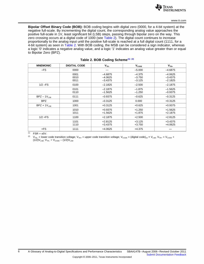
Bipolar Offset Binary Code (BOB): BOB coding begins with digital zero (0000, for a 4-bit system) at thenegative full-scale. By incrementing the digital count, the corresponding analog value approaches thepositive full-scale in 1V, least significant bit (LSB) steps, passing through bipolar zero on the way. Thiszero crossing occurs at a digital code of 1000 (see Table 2). The digital count continues to increaseproportionally to the analog input until the positive full-scale is reached at a full digital count (1111, for a4-bit system) as seen in Table 2. With BOB coding, the MSB can be considered a sign indicator, whereasa logic '0' indicates a negative analog value, and a logic '1' indicates an analog value greater than or equalto Bipolar Zero (BPZ).
Table 2. BOB Coding Scheme (1) (2)
MNEMONIC DIGITAL CODE VTR– VCODE VTR+
–FS 0000 — –5.000 –4.6875
0001 –4.6875 –4.375 –4.06250010 –4.0625 –3.750 –3.43750011 –3.4375 –3.125 –2.1825
1/2 –FS 0100 –2.1825 –2.500 –2.1875
0101 –2.1875 –1.875 –1.56250110 –1.5625 –1.250 –0.9375
BPZ – 1VLSB 0111 –0.9375 –0.625 –0.3125
BPZ 1000 –0.3125 0.000 +0.3125
BPZ + 1VLSB 1001 +0.3125 +0.625 +0.9375
1010 +0.9375 +1.250 +1.56251011 +1.5625 +1.875 +2.1875
1/2 +FS 1100 +2.1875 +2.500 +2.8125
1101 +2.8125 +3.125 +3.43751110 +3.4375 +3.750 +4.0625
+FS 1111 +4.0625 +4.375 —(1) FSR = ±5V.(2) VTR– = lower code transition voltage; VTR+ = upper code transition voltage; VCODE = (digital code)10 × VLSB, VTR+ = VCODE +
(1/2)VLSB; VTR– = VCODE – (1/2)VLSB.
6 A Glossary of Analog-to-Digital Specifications and Performance Characteristics SBAA147B–August 2006–Revised October 2011Submit Documentation Feedback
Copyright © 2006–2011, Texas Instruments Incorporated
t =j (ta + t )c
2 2
SNR = 20log10( )1
(2 f t )p j
www.ti.com
Calibration:• Background Calibration–
Background calibrations are pre-programmed and occur at a scheduled frequency during converteroperation without further instructions. During a background calibration, the converter is disconnectedfrom the input signal and an internal offset and/or gain calibration occurs. The results for eachcalibration are stored in the internal registers of the converter and applied to every conversion after thecalibration occurs. The converter algorithm subsequently adds or subtracts the offset calibration valuewith every conversion result. The converter algorithm also divides the gain calibration value with everyconversion.
• Self-Calibration–On command, a self-calibration occurs as the converter is disconnected from the input signal. Oncethis calibration occurs, the converter performs an internal offset and/or gain calibration algorithm. Theconverter algorithm subsequently adds or subtracts the offset calibration value with every conversionresult. The converter algorithm also divides the gain calibration value with every conversion.
• System Calibration–On command, a system calibration occurs with the input signal connected. In this mode, the convertercalibrates offset and gain, including the external input signal(s), on two separate commands. The offsetcalibration is performed with the assumed zero applied to the input of the converter. The converteralgorithm subsequently adds or subtracts the offset calibration value with every following conversionresult. The user can then perform the gain calibration with an assumed full-scale signal applied to theinput. The converter algorithm also divides the gain calibration value with every following conversion.
Clock:• Duty Cycle–
The duty cycle of a clock signal is the ratio of the time the clock signal remains at a logic high (clockpulse width) to the period of the clock signal. Duty cycle is typically expressed as a percentage value.The duty cycle of a perfect square wave or a differential sine wave is 50%.
• Jitter–The standard deviation of clocking the A/D converter sampling edge (can be a rising edge or fallingedge, depending on the specific A/D converter) variation from pulse-to-pulse in time. This instability ofthe clock signal may cause converter errors as well as an increase in converter noise.
The total jitter includes both aperture and clock jitter, and is equal to:
Where:• ta is the root-mean-square of the aperture jitter;• tc is the root-mean-square of the clock jitter
There is no correlation between the clock-jitter and aperture-jitter terms; therefore, these terms can becombined on a root-sum-square basis (rss). In most cases, the clock jitter is several times higher thanthe A/D converter aperture jitter, making the clock jitter the dominant jitter noise source in the system.
Clock jitter can impact the SNR of the converter at medium and higher frequencies. The aperture jitter,along with clock jitter of the sampling system, impacts the overall SNR of the conversion. Thecontribution of jitter to the SNR of the conversion is equal to:
Where:• tj is the clock and aperture jitter;• f is the clock frequency of the converter
• Slew Rate–The time derivative (δV/δt) of the clock signal (digital input or digital output) as it passes through thelogic, voltage threshold.
7SBAA147B–August 2006–Revised October 2011 A Glossary of Analog-to-Digital Specifications and Performance CharacteristicsSubmit Documentation Feedback
Copyright © 2006–2011, Texas Instruments Incorporated
000
Analog Input Voltage
001
010
011
100
101
110
111
Digital
Output
Code
FS1/2 FS 3/4 FS1/4 FS0
Transition point = where
output code changes
from one code
to an adjacent code
Ideal transfer function
for a 3-bit A/D
Transition
Points
code widthIdeal code width =
1LSB
000
Analog Input
001
010
011
100
101
110
111
Dig
ital O
utp
ut
FS1/2 FS0
Code
under test
50%0%
100%
Transition point; uncertainty noise
Center of code width
Low side transition
f K = f NS t
· ·
www.ti.com
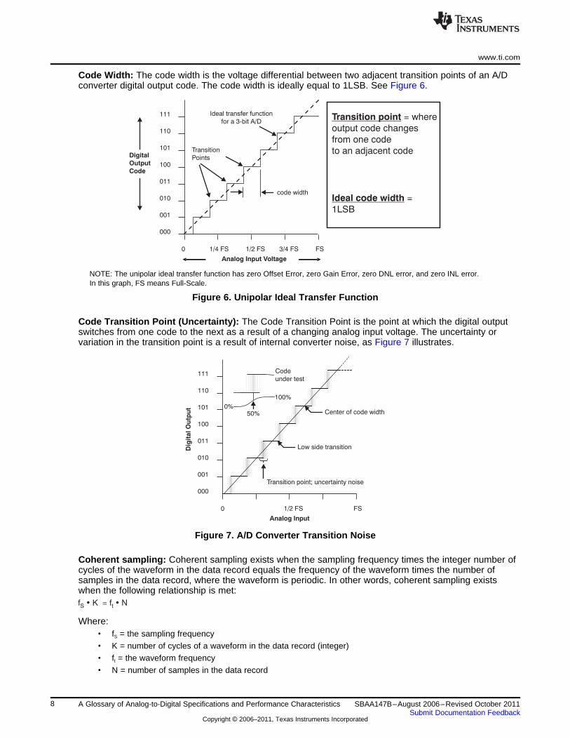
Code Width: The code width is the voltage differential between two adjacent transition points of an A/Dconverter digital output code. The code width is ideally equal to 1LSB. See Figure 6.
NOTE: The unipolar ideal transfer function has zero Offset Error, zero Gain Error, zero DNL error, and zero INL error.In this graph, FS means Full-Scale.
Figure 6. Unipolar Ideal Transfer Function
Code Transition Point (Uncertainty): The Code Transition Point is the point at which the digital outputswitches from one code to the next as a result of a changing analog input voltage. The uncertainty orvariation in the transition point is a result of internal converter noise, as Figure 7 illustrates.
Figure 7. A/D Converter Transition Noise
Coherent sampling: Coherent sampling exists when the sampling frequency times the integer number ofcycles of the waveform in the data record equals the frequency of the waveform times the number ofsamples in the data record, where the waveform is periodic. In other words, coherent sampling existswhen the following relationship is met:
Where:• fS = the sampling frequency• K = number of cycles of a waveform in the data record (integer)• ft = the waveform frequency• N = number of samples in the data record
8 A Glossary of Analog-to-Digital Specifications and Performance Characteristics SBAA147B–August 2006–Revised October 2011Submit Documentation Feedback
Copyright © 2006–2011, Texas Instruments Incorporated
www.ti.com
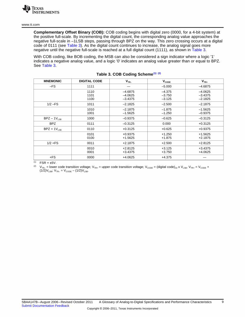
Complementary Offset Binary (COB): COB coding begins with digital zero (0000, for a 4-bit system) atthe positive full-scale. By incrementing the digital count, the corresponding analog value approaches thenegative full-scale in –1LSB steps, passing through BPZ on the way. This zero crossing occurs at a digitalcode of 0111 (see Table 3). As the digital count continues to increase, the analog signal goes morenegative until the negative full-scale is reached at a full digital count (1111), as shown in Table 3.
With COB coding, like BOB coding, the MSB can also be considered a sign indicator where a logic '1'indicates a negative analog value, and a logic '0' indicates an analog value greater than or equal to BPZ.See Table 3.
Table 3. COB Coding Scheme (1) (2)
MNEMONIC DIGITAL CODE VTR– VCODE VTR+
–FS 1111 — –5.000 –4.6875
1110 –4.6875 –4.375 –4.06251101 –4.0625 –3.750 –3.43751100 –3.4375 –3.125 –2.1825
1/2 –FS 1011 –2.1825 –2.500 –2.1875
1010 –2.1875 –1.875 –1.56251001 –1.5625 –1.250 –0.9375
BPZ – 1VLSB 1000 –0.9375 –0.625 –0.3125
BPZ 0111 –0.3125 0.000 +0.3125
BPZ + 1VLSB 0110 +0.3125 +0.625 +0.9375
0101 +0.9375 +1.250 +1.56250100 +1.5625 +1.875 +2.1875
1/2 +FS 0011 +2.1875 +2.500 +2.8125
0010 +2.8125 +3.125 +3.43750001 +3.4375 +3.750 +4.0625
+FS 0000 +4.0625 +4.375 —(1) FSR = ±5V.(2) VTR– = lower code transition voltage; VTR+ = upper code transition voltage; VCODE = (digital code)10 x VLSB, VTR+ = VCODE +
(1/2)VLSB; VTR– = VCODE – (1/2)VLSB.
9SBAA147B–August 2006–Revised October 2011 A Glossary of Analog-to-Digital Specifications and Performance CharacteristicsSubmit Documentation Feedback
Copyright © 2006–2011, Texas Instruments Incorporated
www.ti.com
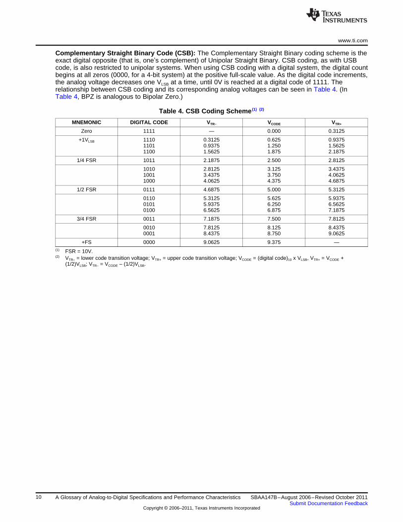
Complementary Straight Binary Code (CSB): The Complementary Straight Binary coding scheme is theexact digital opposite (that is, one’s complement) of Unipolar Straight Binary. CSB coding, as with USBcode, is also restricted to unipolar systems. When using CSB coding with a digital system, the digital countbegins at all zeros (0000, for a 4-bit system) at the positive full-scale value. As the digital code increments,the analog voltage decreases one VLSB at a time, until 0V is reached at a digital code of 1111. Therelationship between CSB coding and its corresponding analog voltages can be seen in Table 4. (InTable 4, BPZ is analogous to Bipolar Zero.)
Table 4. CSB Coding Scheme (1) (2)
MNEMONIC DIGITAL CODE VTR– VCODE VTR+
Zero 1111 — 0.000 0.3125
+1VLSB 1110 0.3125 0.625 0.93751101 0.9375 1.250 1.56251100 1.5625 1.875 2.1875
1/4 FSR 1011 2.1875 2.500 2.8125
1010 2.8125 3.125 3.43751001 3.4375 3.750 4.06251000 4.0625 4.375 4.6875
1/2 FSR 0111 4.6875 5.000 5.3125
0110 5.3125 5.625 5.93750101 5.9375 6.250 6.56250100 6.5625 6.875 7.1875
3/4 FSR 0011 7.1875 7.500 7.8125
0010 7.8125 8.125 8.43750001 8.4375 8.750 9.0625
+FS 0000 9.0625 9.375 —(1) FSR = 10V.(2) VTR– = lower code transition voltage; VTR+ = upper code transition voltage; VCODE = (digital code)10 x VLSB, VTR+ = VCODE +
(1/2)VLSB; VTR– = VCODE – (1/2)VLSB.
10 A Glossary of Analog-to-Digital Specifications and Performance Characteristics SBAA147B–August 2006–Revised October 2011Submit Documentation Feedback
Copyright © 2006–2011, Texas Instruments Incorporated
www.ti.com
Common-mode, DC:• Error–
Common-mode error is the change in output code when the two differential inputs are changed by anequal amount. This specification applies where a converter has a differential input, AIN+ and AIN–. Thisterm is usually specified in LSBs.
• Range–The common-mode, analog voltage range at the differential input of the A/D converter while theconverter still converts accurate code in accordance with the specific device limits. This specificationapplies when the input voltages applied to the converters has a relatively small differential input, AIN+
and AIN–.
• Signal–The input common-mode signal is equal to (AIN+ + AIN–) / 2. Another name for this specification isCommon-mode Voltage. This specification applies when the input voltages applied to a converter havea differential input, AIN+ and AIN–.
• Voltage–The common-mode voltage is equal to the sum of the two analog input voltages divided by two.
Common-mode Rejection Ratio (CMRR): The Common-mode Rejection Ratio is the degree of rejectionof a common-mode signal (dc or ac) across the differential input stage. This specification is the ratio of theresulting digital output signal to a changing input common-mode signal.
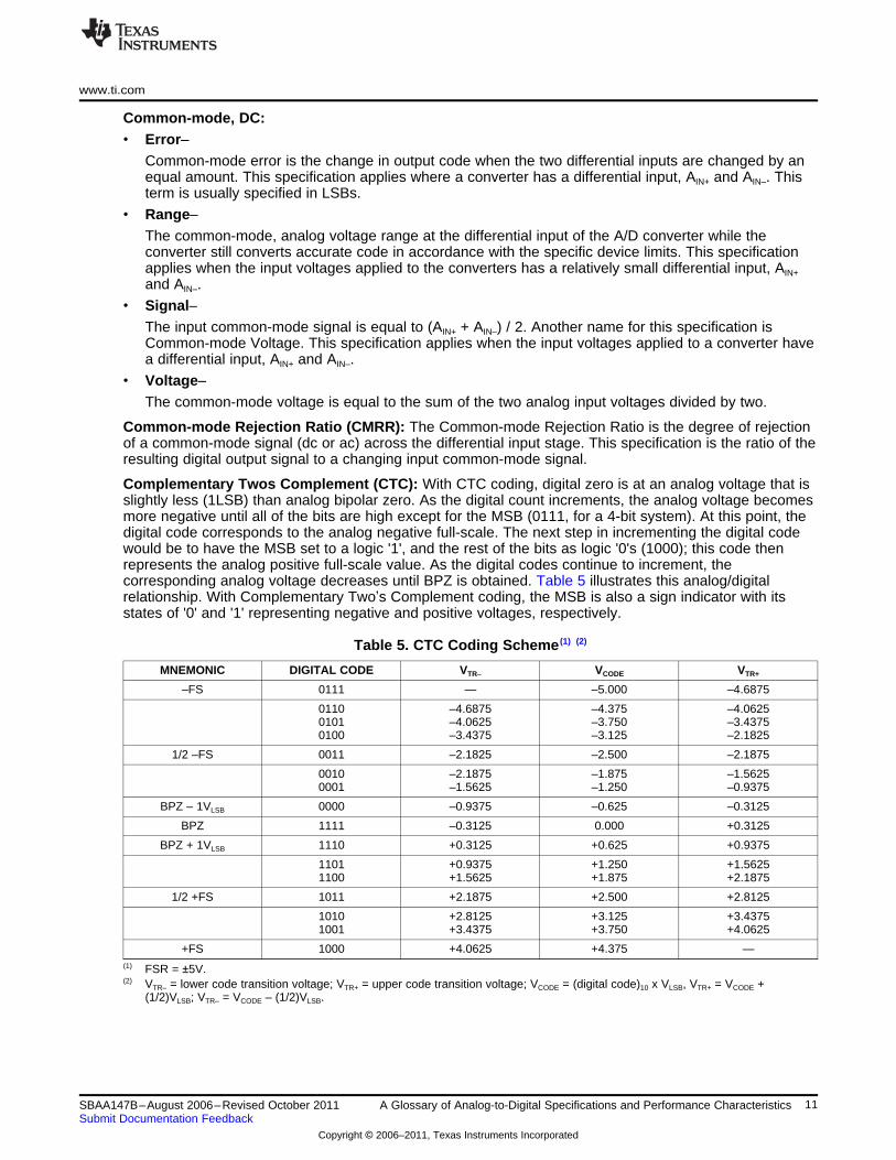
Complementary Twos Complement (CTC): With CTC coding, digital zero is at an analog voltage that isslightly less (1LSB) than analog bipolar zero. As the digital count increments, the analog voltage becomesmore negative until all of the bits are high except for the MSB (0111, for a 4-bit system). At this point, thedigital code corresponds to the analog negative full-scale. The next step in incrementing the digital codewould be to have the MSB set to a logic '1', and the rest of the bits as logic '0's (1000); this code thenrepresents the analog positive full-scale value. As the digital codes continue to increment, thecorresponding analog voltage decreases until BPZ is obtained. Table 5 illustrates this analog/digitalrelationship. With Complementary Two’s Complement coding, the MSB is also a sign indicator with itsstates of '0' and '1' representing negative and positive voltages, respectively.
Table 5. CTC Coding Scheme (1) (2)
MNEMONIC DIGITAL CODE VTR– VCODE VTR+
–FS 0111 — –5.000 –4.6875
0110 –4.6875 –4.375 –4.06250101 –4.0625 –3.750 –3.43750100 –3.4375 –3.125 –2.1825
1/2 –FS 0011 –2.1825 –2.500 –2.1875
0010 –2.1875 –1.875 –1.56250001 –1.5625 –1.250 –0.9375
BPZ – 1VLSB 0000 –0.9375 –0.625 –0.3125
BPZ 1111 –0.3125 0.000 +0.3125
BPZ + 1VLSB 1110 +0.3125 +0.625 +0.9375
1101 +0.9375 +1.250 +1.56251100 +1.5625 +1.875 +2.1875
1/2 +FS 1011 +2.1875 +2.500 +2.8125
1010 +2.8125 +3.125 +3.43751001 +3.4375 +3.750 +4.0625
+FS 1000 +4.0625 +4.375 —(1) FSR = ±5V.(2) VTR– = lower code transition voltage; VTR+ = upper code transition voltage; VCODE = (digital code)10 x VLSB, VTR+ = VCODE +
(1/2)VLSB; VTR– = VCODE – (1/2)VLSB.
11SBAA147B–August 2006–Revised October 2011 A Glossary of Analog-to-Digital Specifications and Performance CharacteristicsSubmit Documentation Feedback
Copyright © 2006–2011, Texas Instruments Incorporated
Passband Stop bandTransition
band
Frequency (Hz)
APASS
AMAX
ASTOP
Gain (dB)M = filter order
fCUT-OFF
fSTOP
e
www.ti.com
Conversion Cycle: A conversion cycle is a discrete A/D converter operation, and refers to the process ofchanging the input signal to a digital result. When performed by a SAR converter, for example, theconversion occurs after the sample is acquired. For delta-sigma converters, a conversion cycle refers tothe tDATA time period (that is, the period between each data output). With delta-sigma converters, eachdigital output is actually based on the modulator results from several tDATA time periods.
Conversion Maximum Rate: The maximum sampling rate of a device while performing within specifiedoperating limits. All parametric testing is performed at this sampling rate unless otherwise noted. (Also seeSample Rate.)
Conversion Minimum Rate: The minimum conversion rate is the minimum sampling rate at which theA/D converter meets its stated specifications.
Conversion Rate: The frequency of the digital output words at the output of the converter. (See alsoSample Rate.)
Conversion Speed: See Sample Rate.
Conversion Time: After sampling the signal, the conversion time is the time required for a SAR orpipeline A/D converter to complete a single conversion. The conversion time does not include theacquisition time or multiplexer set-up time. The conversion time for a given device is less than thethroughput time.
Crosstalk: This term refers the condition in which a signal affects another nearby signal. With A/Dconverters, this event is the occurrence of an undesirable signal coupling across a multi-channel A/Dconverter from one channel that is not being used in the conversion to another channel that is part of thesignal path. This undesired coupling is a result of capacitive or conductive coupling from one channel toanother. This interference appears as noise in the output digital code.
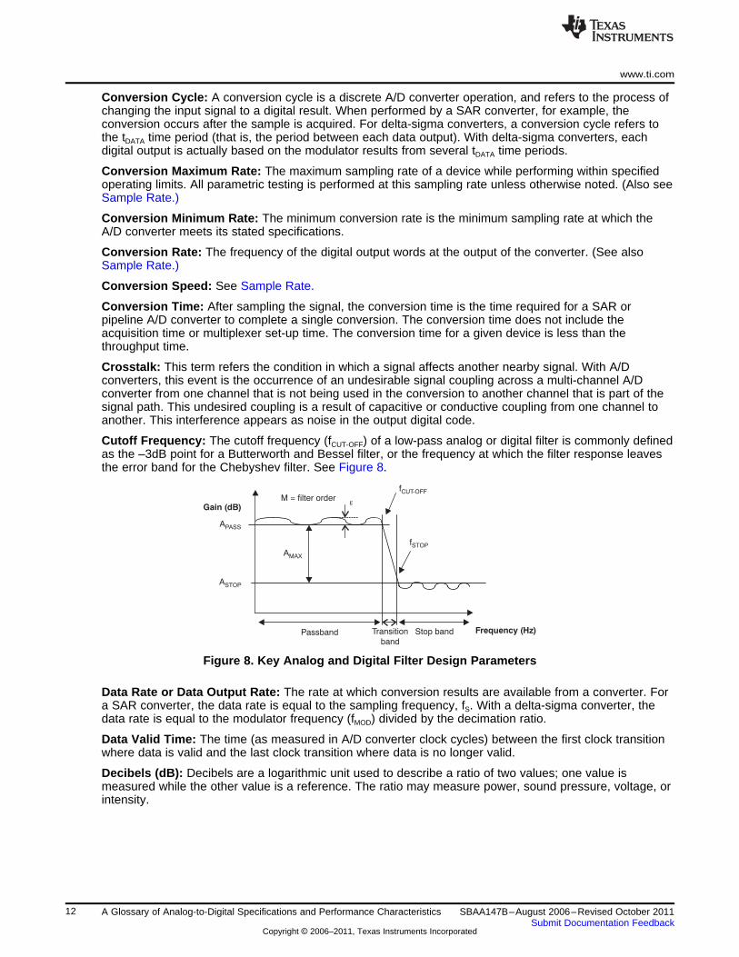
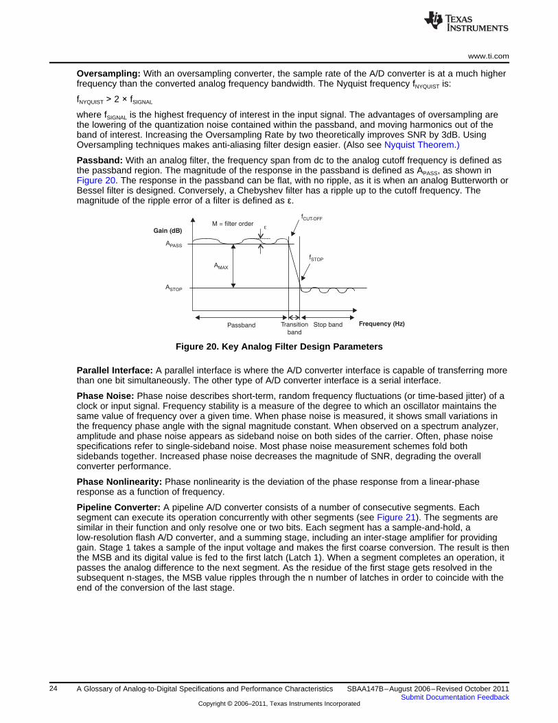
Cutoff Frequency: The cutoff frequency (fCUT-OFF) of a low-pass analog or digital filter is commonly definedas the –3dB point for a Butterworth and Bessel filter, or the frequency at which the filter response leavesthe error band for the Chebyshev filter. See Figure 8.
Figure 8. Key Analog and Digital Filter Design Parameters
Data Rate or Data Output Rate: The rate at which conversion results are available from a converter. Fora SAR converter, the data rate is equal to the sampling frequency, fS. With a delta-sigma converter, thedata rate is equal to the modulator frequency (fMOD) divided by the decimation ratio.
Data Valid Time: The time (as measured in A/D converter clock cycles) between the first clock transitionwhere data is valid and the last clock transition where data is no longer valid.
Decibels (dB): Decibels are a logarithmic unit used to describe a ratio of two values; one value ismeasured while the other value is a reference. The ratio may measure power, sound pressure, voltage, orintensity.
12 A Glossary of Analog-to-Digital Specifications and Performance Characteristics SBAA147B–August 2006–Revised October 2011Submit Documentation Feedback
Copyright © 2006–2011, Texas Instruments Incorporated
Analog
Input
Digital
Output
Delta-Sigma
Modulator
Digital
FilterDecimator
Digital Decimating Filter
(usually implemented
as a single unit)
Sample rate (f )S
= DR (decimation ratio)fD
fS
Data rate (f )D
www.ti.com
dBFS: dBFS is the decibel measurement as it is referred to the full-scale input range.
dBc: Decibels referenced to a carrier, or decibels below a carrier. For example, a spurious signal ordistortion less than –40dBc means that the distortion is at least 40dB less than the specified carrier signalor desired signal level.
dBm: dBm represents a measured power level in decibels relative to 1mW.
Decimation Ratio: The decimation ratio is the ratio between the output sampling rate of the delta-sigmamodulator and the output data rate of a delta-sigma converter as performed by the decimator. Thedecimator is a block that decimates or discards some results. The decimation ratio sets the number ofdata samples from the modulator that are averaged together to get a result. Higher decimation ratiosaverage a greater number of values together, thereby producing lower noise results.
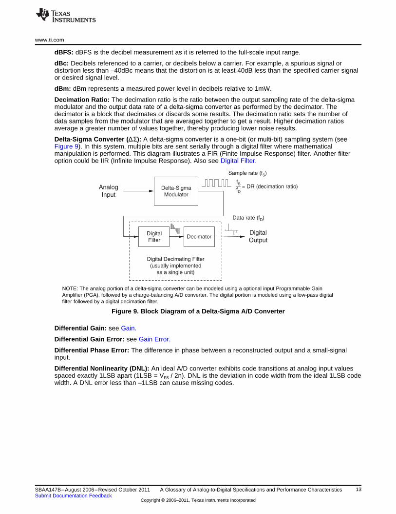
Delta-Sigma Converter (ΔΣ): A delta-sigma converter is a one-bit (or multi-bit) sampling system (seeFigure 9). In this system, multiple bits are sent serially through a digital filter where mathematicalmanipulation is performed. This diagram illustrates a FIR (Finite Impulse Response) filter. Another filteroption could be IIR (Infinite Impulse Response). Also see Digital Filter.
NOTE: The analog portion of a delta-sigma converter can be modeled using a optional input Programmable GainAmplifier (PGA), followed by a charge-balancing A/D converter. The digital portion is modeled using a low-pass digitalfilter followed by a digital decimation filter.
Figure 9. Block Diagram of a Delta-Sigma A/D Converter
Differential Gain: see Gain.
Differential Gain Error: see Gain Error.
Differential Phase Error: The difference in phase between a reconstructed output and a small-signalinput.
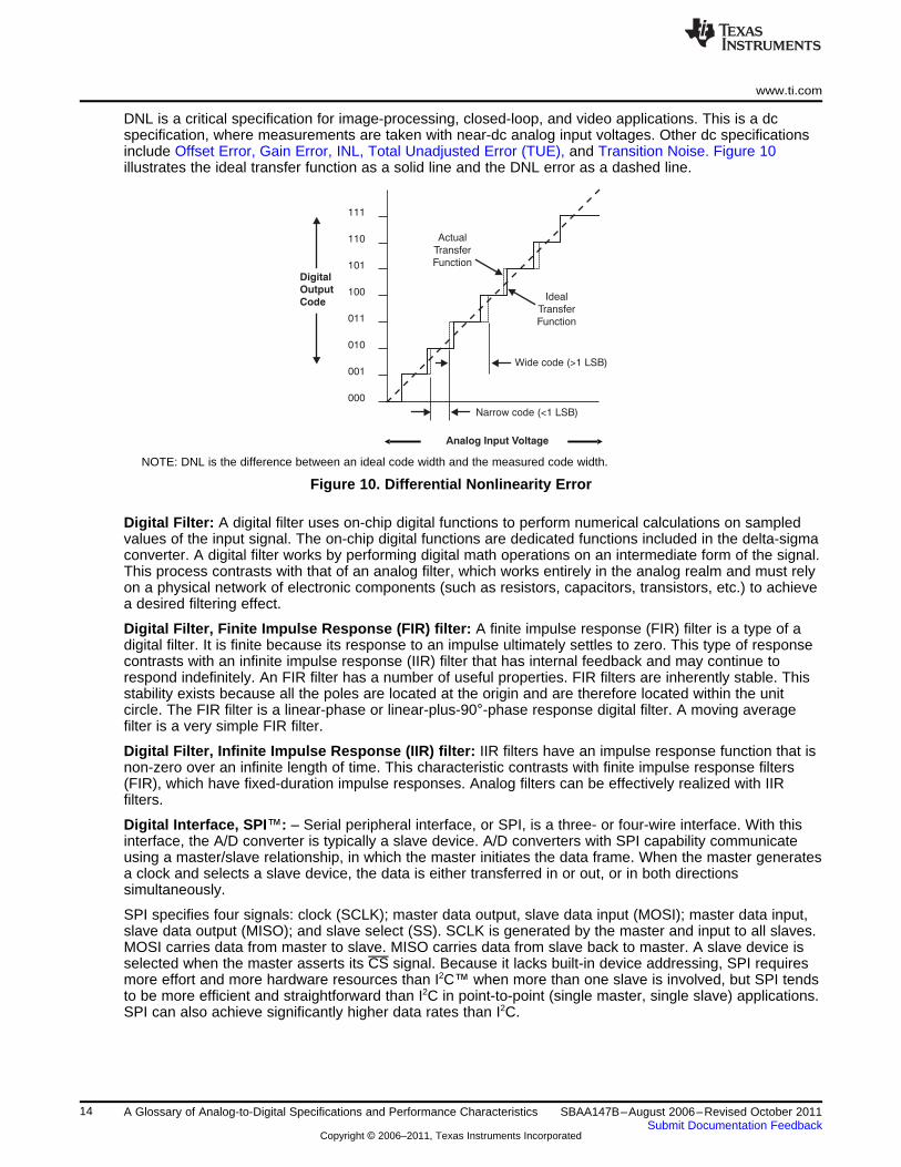
Differential Nonlinearity (DNL): An ideal A/D converter exhibits code transitions at analog input valuesspaced exactly 1LSB apart (1LSB = VFS / 2n). DNL is the deviation in code width from the ideal 1LSB codewidth. A DNL error less than –1LSB can cause missing codes.
13SBAA147B–August 2006–Revised October 2011 A Glossary of Analog-to-Digital Specifications and Performance CharacteristicsSubmit Documentation Feedback
Copyright © 2006–2011, Texas Instruments Incorporated
000
Analog Input Voltage
001
010
011
100
101
110
111
Digital
Output
Code
Narrow code (<1 LSB)
Wide code (>1 LSB)
Actual
Transfer
Function
Ideal
Transfer
Function
www.ti.com
DNL is a critical specification for image-processing, closed-loop, and video applications. This is a dcspecification, where measurements are taken with near-dc analog input voltages. Other dc specificationsinclude Offset Error, Gain Error, INL, Total Unadjusted Error (TUE), and Transition Noise. Figure 10illustrates the ideal transfer function as a solid line and the DNL error as a dashed line.
NOTE: DNL is the difference between an ideal code width and the measured code width.
Figure 10. Differential Nonlinearity Error
Digital Filter: A digital filter uses on-chip digital functions to perform numerical calculations on sampledvalues of the input signal. The on-chip digital functions are dedicated functions included in the delta-sigmaconverter. A digital filter works by performing digital math operations on an intermediate form of the signal.This process contrasts with that of an analog filter, which works entirely in the analog realm and must relyon a physical network of electronic components (such as resistors, capacitors, transistors, etc.) to achievea desired filtering effect.
Digital Filter, Finite Impulse Response (FIR) filter: A finite impulse response (FIR) filter is a type of adigital filter. It is finite because its response to an impulse ultimately settles to zero. This type of responsecontrasts with an infinite impulse response (IIR) filter that has internal feedback and may continue torespond indefinitely. An FIR filter has a number of useful properties. FIR filters are inherently stable. Thisstability exists because all the poles are located at the origin and are therefore located within the unitcircle. The FIR filter is a linear-phase or linear-plus-90°-phase response digital filter. A moving averagefilter is a very simple FIR filter.
Digital Filter, Infinite Impulse Response (IIR) filter: IIR filters have an impulse response function that isnon-zero over an infinite length of time. This characteristic contrasts with finite impulse response filters(FIR), which have fixed-duration impulse responses. Analog filters can be effectively realized with IIRfilters.
Digital Interface, SPI™: – Serial peripheral interface, or SPI, is a three- or four-wire interface. With thisinterface, the A/D converter is typically a slave device. A/D converters with SPI capability communicateusing a master/slave relationship, in which the master initiates the data frame. When the master generatesa clock and selects a slave device, the data is either transferred in or out, or in both directionssimultaneously.
SPI specifies four signals: clock (SCLK); master data output, slave data input (MOSI); master data input,slave data output (MISO); and slave select (SS). SCLK is generated by the master and input to all slaves.MOSI carries data from master to slave. MISO carries data from slave back to master. A slave device isselected when the master asserts its CS signal. Because it lacks built-in device addressing, SPI requiresmore effort and more hardware resources than I2C™ when more than one slave is involved, but SPI tendsto be more efficient and straightforward than I2C in point-to-point (single master, single slave) applications.SPI can also achieve significantly higher data rates than I2C.
14 A Glossary of Analog-to-Digital Specifications and Performance Characteristics SBAA147B–August 2006–Revised October 2011Submit Documentation Feedback
Copyright © 2006–2011, Texas Instruments Incorporated
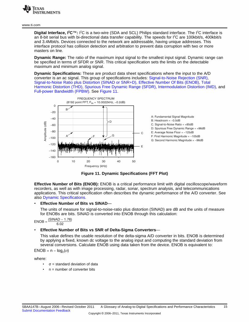
A: Fundamental Signal Magnitude
B: Headroom = 0.5dB
C. Signal-to-Noise Ratio = 85dB
D: Spurious Free Dynamic Range = 96dB
E: Average Noise Floor = 125dB
F: First Harmonic Magnitude = 105dB
G: Second Harmonic Magnitude = 96dB
-
-
-
-
+
+
A
B
C
D
E
F G
0
-20
-40
-60
-80
-100
-120
-140
-160
Am
plit
ud
e (
dB
)
0 10 20 30 40 50
Frequency (kHz)
FREQUENCY SPECTRUM
(8192 point FFT, F = 10.0022kHz, 0.2dB)IN -
ENOB =(SINAD 1.76)
6.02
-
ENOB = 2n log ( )- s
www.ti.com
Digital Interface, I2C™: I2C is a two-wire (SDA and SCL) Philips standard interface. The I2C interface isan 8-bit serial bus with bi-directional data transfer capability. The speeds for I2C are 100kbit/s, 400kbit/sand 3.4Mbit/s. Devices connected to the network are addressable, having unique addresses. Thisinterface protocol has collision detection and arbitration to prevent data corruption with two or moremasters on line.
Dynamic Range: The ratio of the maximum input signal to the smallest input signal. Dynamic range canbe specified in terms of SFDR or SNR. This critical specification sets the limits on the detectablemaximum and minimum analog signal.
Dynamic Specifications: These are product data sheet specifications where the input to the A/Dconverter is an ac signal. This group of specifications includes: Signal-to-Noise Rejection (SNR),Signal-to-Noise Ratio plus Distortion (SINAD or SNR+D), Effective Number Of Bits (ENOB), TotalHarmonic Distortion (THD), Spurious Free Dynamic Range (SFDR), Intermodulation Distortion (IMD), andFull-power Bandwidth (FPBW). See Figure 11.
Figure 11. Dynamic Specifications (FFT Plot)
Effective Number of Bits (ENOB): ENOB is a critical performance limit with digital oscilloscope/waveformrecorders, as well as with image processing, radar, sonar, spectrum analysis, and telecommunicationsapplications. This critical specification often describes the dynamic performance of the A/D converter. Seealso Dynamic Specifications.
• Effective Number of Bits vs SINAD—The units of measure for signal-to-noise-ratio plus distortion (SINAD) are dB and the units of measurefor ENOBs are bits. SINAD is converted into ENOB through this calculation:
• Effective Number of Bits vs SNR of Delta-Sigma Converters—This value defines the usable resolution of the delta-sigma A/D converter in bits. ENOB is determinedby applying a fixed, known dc voltage to the analog input and computing the standard deviation fromseveral conversions. Calculate ENOB using data taken from the device. ENOB is equivalent to:
where:• σ = standard deviation of data• n = number of converter bits
15SBAA147B–August 2006–Revised October 2011 A Glossary of Analog-to-Digital Specifications and Performance CharacteristicsSubmit Documentation Feedback
Copyright © 2006–2011, Texas Instruments Incorporated
www.ti.com
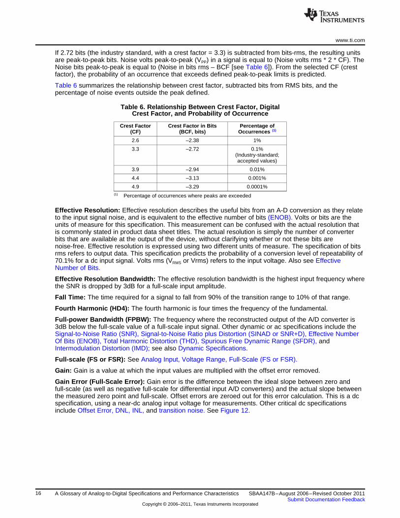
If 2.72 bits (the industry standard, with a crest factor = 3.3) is subtracted from bits-rms, the resulting unitsare peak-to-peak bits. Noise volts peak-to-peak (VPP) in a signal is equal to (Noise volts rms * 2 * CF). TheNoise bits peak-to-peak is equal to (Noise in bits rms – BCF [see Table 6]). From the selected CF (crestfactor), the probability of an occurrence that exceeds defined peak-to-peak limits is predicted.
Table 6 summarizes the relationship between crest factor, subtracted bits from RMS bits, and thepercentage of noise events outside the peak defined.
Table 6. Relationship Between Crest Factor, DigitalCrest Factor, and Probability of Occurrence
Crest Factor Crest Factor in Bits Percentage of(CF) (BCF, bits) Occurrences (1)
2.6 –2.38 1%
3.3 –2.72 0.1%(Industry-standard;accepted values)
3.9 –2.94 0.01%
4.4 –3.13 0.001%
4.9 –3.29 0.0001%(1) Percentage of occurrences where peaks are exceeded
Effective Resolution: Effective resolution describes the useful bits from an A-D conversion as they relateto the input signal noise, and is equivalent to the effective number of bits (ENOB). Volts or bits are theunits of measure for this specification. This measurement can be confused with the actual resolution thatis commonly stated in product data sheet titles. The actual resolution is simply the number of converterbits that are available at the output of the device, without clarifying whether or not these bits arenoise-free. Effective resolution is expressed using two different units of measure. The specification of bitsrms refers to output data. This specification predicts the probability of a conversion level of repeatability of70.1% for a dc input signal. Volts rms (VRMS or Vrms) refers to the input voltage. Also see EffectiveNumber of Bits.
Effective Resolution Bandwidth: The effective resolution bandwidth is the highest input frequency wherethe SNR is dropped by 3dB for a full-scale input amplitude.
Fall Time: The time required for a signal to fall from 90% of the transition range to 10% of that range.
Fourth Harmonic (HD4): The fourth harmonic is four times the frequency of the fundamental.
Full-power Bandwidth (FPBW): The frequency where the reconstructed output of the A/D converter is3dB below the full-scale value of a full-scale input signal. Other dynamic or ac specifications include theSignal-to-Noise Ratio (SNR), Signal-to-Noise Ratio plus Distortion (SINAD or SNR+D), Effective NumberOf Bits (ENOB), Total Harmonic Distortion (THD), Spurious Free Dynamic Range (SFDR), andIntermodulation Distortion (IMD); see also Dynamic Specifications.
Full-scale (FS or FSR): See Analog Input, Voltage Range, Full-Scale (FS or FSR).
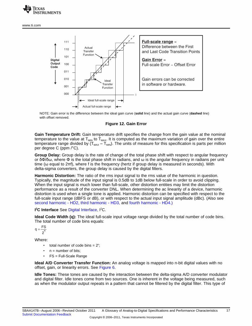
Gain: Gain is a value at which the input values are multiplied with the offset error removed.
Gain Error (Full-Scale Error): Gain error is the difference between the ideal slope between zero andfull-scale (as well as negative full-scale for differential input A/D converters) and the actual slope betweenthe measured zero point and full-scale. Offset errors are zeroed out for this error calculation. This is a dcspecification, using a near-dc analog input voltage for measurements. Other critical dc specificationsinclude Offset Error, DNL, INL, and transition noise. See Figure 12.
16 A Glossary of Analog-to-Digital Specifications and Performance Characteristics SBAA147B–August 2006–Revised October 2011Submit Documentation Feedback
Copyright © 2006–2011, Texas Instruments Incorporated
000
001
010
011
100
101
110
111
Digital
Output
Code
Actual full-scale range
Ideal full-scale range
Actual
Transfer
Function
Ideal
Transfer
Function
Full-scale range =
Difference between the First
and Last Code Transition Points
Gain Error =
Full-scale Error Offset Error-
Gain errors can be corrected
in software or hardware.
q =FS
2n
www.ti.com
NOTE: Gain error is the difference between the ideal gain curve (solid line) and the actual gain curve (dashed line)with offset removed.
Figure 12. Gain Error
Gain Temperature Drift: Gain temperature drift specifies the change from the gain value at the nominaltemperature to the value at TMIN to TMAX. It is computed as the maximum variation of gain over the entiretemperature range divided by (TMAX – TMIN). The units of measure for this specification is parts per millionper degree C (ppm /°C).
Group Delay: Group delay is the rate of change of the total phase shift with respect to angular frequencyor δΦ/δω, where Φ is the total phase shift in radians, and ω is the angular frequency in radians per unittime (ω equal to 2πf), where f is the frequency (hertz if group delay is measured in seconds). Withdelta-sigma converters, the group delay is caused by the digital filters.
Harmonic Distortion: The ratio of the rms input signal to the rms value of the harmonic in question.Typically, the magnitude of the input signal is 0.5dB to 1dB below full-scale in order to avoid clipping.When the input signal is much lower than full-scale, other distortion entities may limit the distortionperformance as a result of the converter DNL. When determining the ac linearity of a device, harmonicdistortion is used when a single tone is applied. Harmonic distortion can be specified with respect to thefull-scale input range (dBFS or dB), or with respect to the actual input signal amplitude (dBc). (Also seesecond harmonic - HD2, third harmonic - HD3, and fourth harmonic - HD4.)
I2C Interface See Digital Interface, I2C.
Ideal Code Width (q): The ideal full-scale input voltage range divided by the total number of code bins.The total number of code bins equals:
Where:• total number of code bins = 2n;• n = number of bits;• FS = Full-Scale Range
Ideal A/D Converter Transfer Function: An analog voltage is mapped into n-bit digital values with nooffset, gain, or linearity errors. See Figure 6.
Idle Tones: These tones are caused by the interaction between the delta-sigma A/D converter modulatorand digital filter. Idle tones come from two sources. One is inherent in the voltage being measured, suchas when the modulator output repeats in a pattern that cannot be filtered by the digital filter. This type of
17SBAA147B–August 2006–Revised October 2011 A Glossary of Analog-to-Digital Specifications and Performance CharacteristicsSubmit Documentation Feedback
Copyright © 2006–2011, Texas Instruments Incorporated
000
Analog Input Voltage
001
010
011
100
101
110
111
Digital
Output
Code
INL < 0
Actual
Transfer
Function
Ideal
Transfer
Function
INL < 0
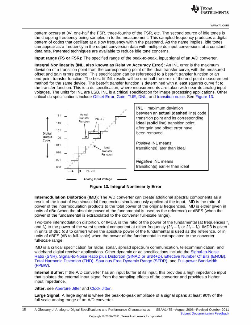
INL = maximum deviation
between an ( line) code
transition point and its corresponding
( line) transition point,
after gain and offset error have
been removed.
actual dashed
ideal solid
Positive INL means
transition(s) later than ideal
Negative INL means
transition(s) earlier than ideal
www.ti.com
pattern occurs at 0V, one-half the FSR, three-fourths of the FSR, etc. The second source of idle tones isthe chopping frequency being sampled in to the measurement. This sampled frequency produces a digitalpattern of codes that oscillate at a slow frequency within the passband. As the name implies, idle tonescan appear as a frequency in the output conversion data with multiple dc input conversions at a constantdata rate. Patented techniques are available to reduce idle tone concerns.
Input range (FS or FSR): The specified range of the peak-to-peak, input signal of an A/D converter.
Integral Nonlinearity (INL, also known as Relative Accuracy Error): An INL error is the maximumdeviation of a transition point from the corresponding point of the ideal transfer curve, with the measuredoffset and gain errors zeroed. This specification can be referenced to a best-fit transfer function or anend-point transfer function. The best-fit INL results will be one-half the error of the end-point measurementmethod for the same device. The best-fit transfer function is determined with a least squares curve fit tothe transfer function. This is a dc specification, where measurements are taken with near-dc analog inputvoltages. The units for INL are LSB. INL is a critical specification for image processing applications. Othercritical dc specifications include Offset Error, Gain, TUE, DNL, and transition noise. See Figure 13.
Figure 13. Integral Nonlinearity Error
Intermodulation Distortion (IMD): The A/D converter can create additional spectral components as aresult of the input of two sinusoidal frequencies simultaneously applied at the input. IMD is the ratio ofpower of the intermodulation products to the total power of the original frequencies. IMD is either given inunits of dBc (when the absolute power of the fundamental is used as the reference) or dBFS (when thepower of the fundamental is extrapolated to the converter full-scale range).
Two-tone intermodulation distortion, or IMD3, is the ratio of the power of the fundamental (at frequencies f1
and f2) to the power of the worst spectral component at either frequency (2f1 – f2 or 2f2 – f1). IMD3 is givenin units of dBc (dB to carrier) when the absolute power of the fundamental is used as the reference, or inunits of dBFS (dB to full-scale) when the power of the fundamental in extrapolated to the converterfull-scale range.
IMD is a critical specification for radar, sonar, spread spectrum communication, telecommunication, andwideband digital receiver applications. Other dynamic or ac specifications include the Signal-to-NoiseRatio (SNR), Signal-to-Noise Ratio plus Distortion (SINAD or SNR+D), Effective Number Of Bits (ENOB),Total Harmonic Distortion (THD), Spurious Free Dynamic Range (SFDR), and Full-power Bandwidth(FPBW).
Internal Buffer: If the A/D converter has an input buffer at its input, this provides a high impedance inputthat isolates the external input signal from the sampling effects of the converter and provides a higherinput impedance.
Jitter: see Aperture Jitter and Clock Jitter.
Large Signal: A large signal is where the peak-to-peak amplitude of a signal spans at least 90% of thefull-scale analog range of an A/D converter.
18 A Glossary of Analog-to-Digital Specifications and Performance Characteristics SBAA147B–August 2006–Revised October 2011Submit Documentation Feedback
Copyright © 2006–2011, Texas Instruments Incorporated
N 5- N+0
N+0
N+1
N+1
N+2
N+2
N+3
N+3
N+4
N+4
N+5
N+5
N+6
N+6
N+7
N+7
Single-Cycle
Conversion
Data
Invalid
Analog IN
Data OUT
N 5- N-4
N+0
N-3
N+1
N-2
N+2
N-1
N+3
N+0
N+4
N+1
N+5
N+2
N+6
N+3
N+7
Data
Invalid
Analog IN
Data OUT
A. Zero-cycle Latency
B. Four-cycle Latency
Four-cycle latency
Zero-cycle latency
www.ti.com
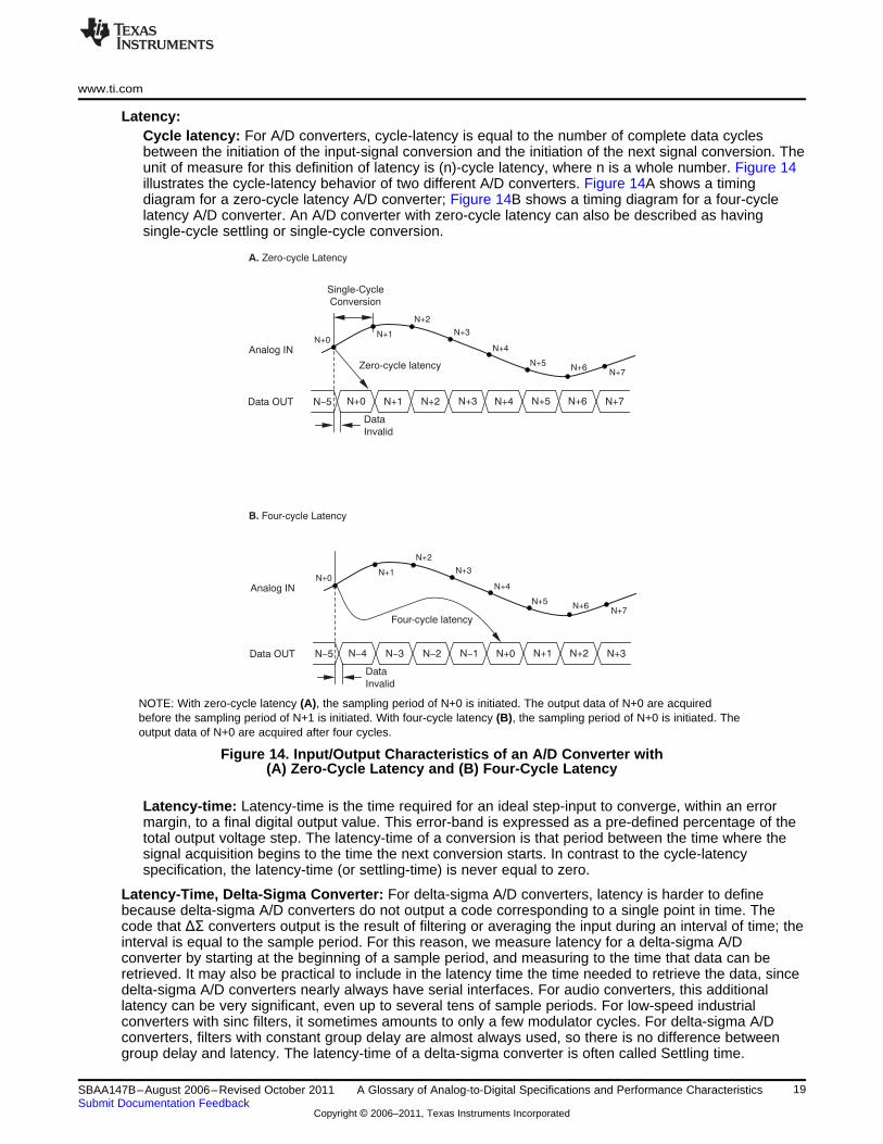
Latency:Cycle latency: For A/D converters, cycle-latency is equal to the number of complete data cyclesbetween the initiation of the input-signal conversion and the initiation of the next signal conversion. Theunit of measure for this definition of latency is (n)-cycle latency, where n is a whole number. Figure 14illustrates the cycle-latency behavior of two different A/D converters. Figure 14A shows a timingdiagram for a zero-cycle latency A/D converter; Figure 14B shows a timing diagram for a four-cyclelatency A/D converter. An A/D converter with zero-cycle latency can also be described as havingsingle-cycle settling or single-cycle conversion.
NOTE: With zero-cycle latency (A), the sampling period of N+0 is initiated. The output data of N+0 are acquiredbefore the sampling period of N+1 is initiated. With four-cycle latency (B), the sampling period of N+0 is initiated. Theoutput data of N+0 are acquired after four cycles.
Figure 14. Input/Output Characteristics of an A/D Converter with(A) Zero-Cycle Latency and (B) Four-Cycle Latency
Latency-time: Latency-time is the time required for an ideal step-input to converge, within an errormargin, to a final digital output value. This error-band is expressed as a pre-defined percentage of thetotal output voltage step. The latency-time of a conversion is that period between the time where thesignal acquisition begins to the time the next conversion starts. In contrast to the cycle-latencyspecification, the latency-time (or settling-time) is never equal to zero.
Latency-Time, Delta-Sigma Converter: For delta-sigma A/D converters, latency is harder to definebecause delta-sigma A/D converters do not output a code corresponding to a single point in time. Thecode that ΔΣ converters output is the result of filtering or averaging the input during an interval of time; theinterval is equal to the sample period. For this reason, we measure latency for a delta-sigma A/Dconverter by starting at the beginning of a sample period, and measuring to the time that data can beretrieved. It may also be practical to include in the latency time the time needed to retrieve the data, sincedelta-sigma A/D converters nearly always have serial interfaces. For audio converters, this additionallatency can be very significant, even up to several tens of sample periods. For low-speed industrialconverters with sinc filters, it sometimes amounts to only a few modulator cycles. For delta-sigma A/Dconverters, filters with constant group delay are almost always used, so there is no difference betweengroup delay and latency. The latency-time of a delta-sigma converter is often called Settling time.
19SBAA147B–August 2006–Revised October 2011 A Glossary of Analog-to-Digital Specifications and Performance CharacteristicsSubmit Documentation Feedback
Copyright © 2006–2011, Texas Instruments Incorporated
Summing
Amplifier
Analog
Input
Integrator
Comparator
(1-bit ADC)
1-bit DAC
Digital
Filter
www.ti.com
Latency-Time, SAR Converter: For SAR A/D converters, latency is typically very short; it is the amountof time needed for the successive approximation process to complete. Data is typically availableimmediately afterward. This approach is typically equal to the conversion time, and exclusive of thesample time. For SARs, which generally have an external continuous-time analog filter at the front-end,group delay can be a more useful measurement, since the latency may be frequency-dependent.
Latency-Time, Pipeline Converter: The number of complete clock cycles between the initiation of aconversion and when the data appears on the output driver stage.
Least Significant Bit (LSB): The least significant bit is the bit representation of the smallest analog inputsignal that is converted, and is synonymous with the code bin width. The least significant bit defines theresolution of the converter. It is also referred to the furthest right bit in a binary digital word.
Major Carry Transition: The mid-scale point where the MSB changes from low to high and all other bitschange from high to low, or where the MSB changes from high to low and all other bits change from low tohigh. These transition points are often where the worst switching noise occurs. (See also Most SignificantBit or MSB.)
Missing Code: A missing code is when a legitimate A/D converter output code that should exist is notavailable. An increase in the analog voltage can produce an unexpected smaller or the same digital outputcode. See Figure 17.
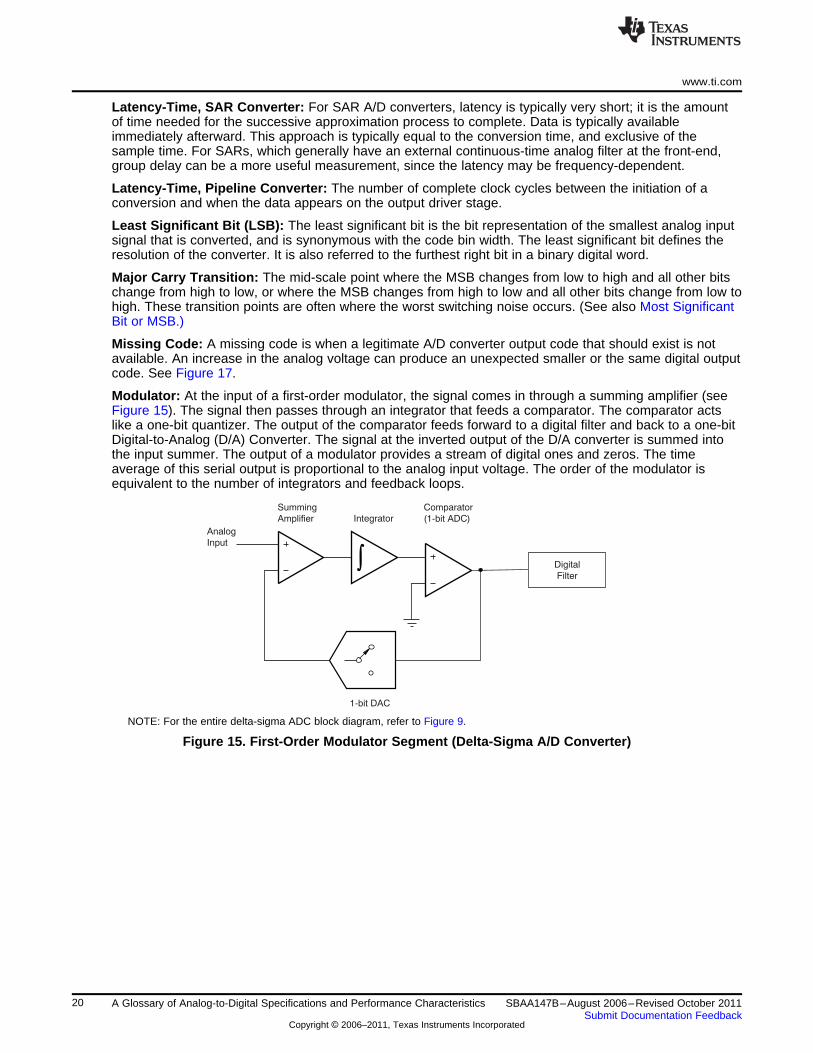
Modulator: At the input of a first-order modulator, the signal comes in through a summing amplifier (seeFigure 15). The signal then passes through an integrator that feeds a comparator. The comparator actslike a one-bit quantizer. The output of the comparator feeds forward to a digital filter and back to a one-bitDigital-to-Analog (D/A) Converter. The signal at the inverted output of the D/A converter is summed intothe input summer. The output of a modulator provides a stream of digital ones and zeros. The timeaverage of this serial output is proportional to the analog input voltage. The order of the modulator isequivalent to the number of integrators and feedback loops.
NOTE: For the entire delta-sigma ADC block diagram, refer to Figure 9.
Figure 15. First-Order Modulator Segment (Delta-Sigma A/D Converter)
20 A Glossary of Analog-to-Digital Specifications and Performance Characteristics SBAA147B–August 2006–Revised October 2011Submit Documentation Feedback
Copyright © 2006–2011, Texas Instruments Incorporated
Analog
IN
Digital
OUT
Integrator Integrator 1-bit ADC
S S
xi
ei
yi
1-bit DAC
000
Analog Input Voltage
001
010
011
100
101
110
111
Digital
Output
Code
FS1/2 FS 3/4 FS1/4 FS0
If the output code
always increases when
the input increases, the
device is .monotonic
Non-monotonic as well as
a missing code
www.ti.com
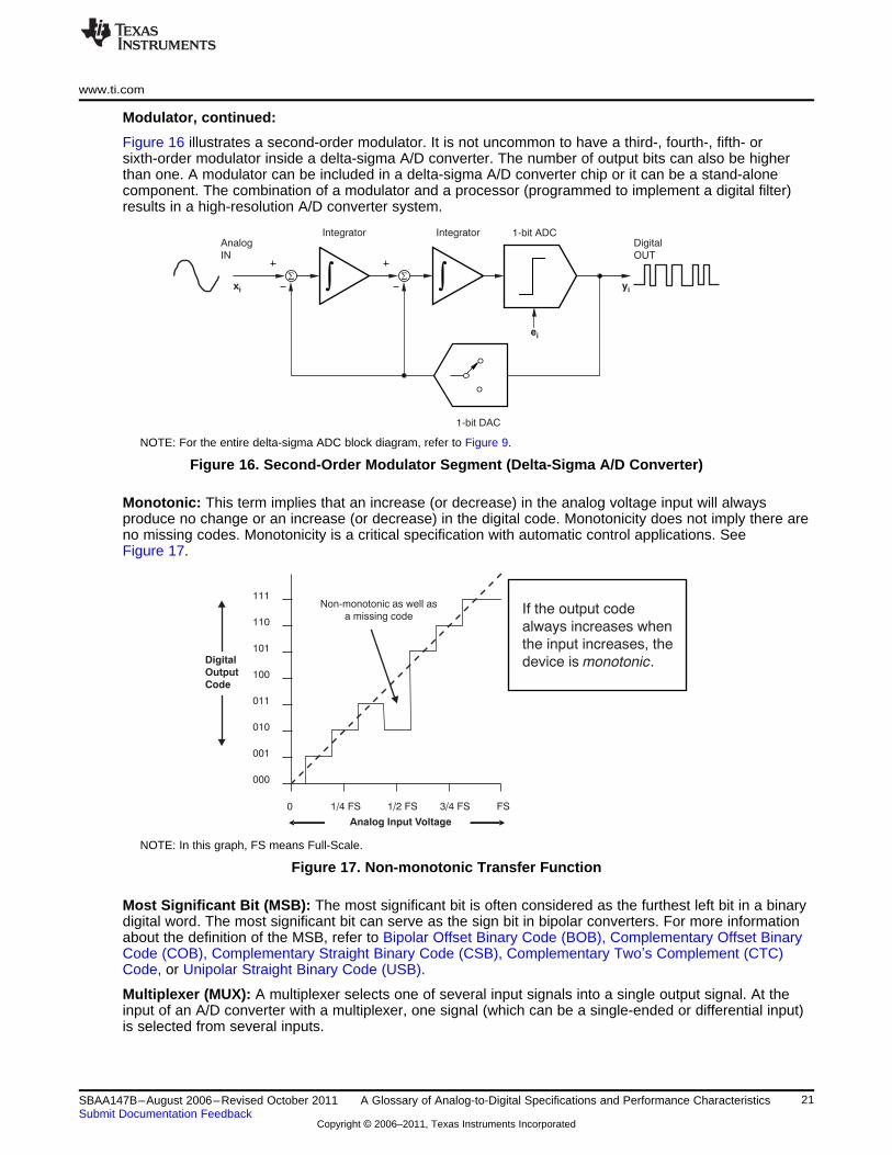
Modulator, continued:
Figure 16 illustrates a second-order modulator. It is not uncommon to have a third-, fourth-, fifth- orsixth-order modulator inside a delta-sigma A/D converter. The number of output bits can also be higherthan one. A modulator can be included in a delta-sigma A/D converter chip or it can be a stand-alonecomponent. The combination of a modulator and a processor (programmed to implement a digital filter)results in a high-resolution A/D converter system.
NOTE: For the entire delta-sigma ADC block diagram, refer to Figure 9.
Figure 16. Second-Order Modulator Segment (Delta-Sigma A/D Converter)
Monotonic: This term implies that an increase (or decrease) in the analog voltage input will alwaysproduce no change or an increase (or decrease) in the digital code. Monotonicity does not imply there areno missing codes. Monotonicity is a critical specification with automatic control applications. SeeFigure 17.
NOTE: In this graph, FS means Full-Scale.
Figure 17. Non-monotonic Transfer Function
Most Significant Bit (MSB): The most significant bit is often considered as the furthest left bit in a binarydigital word. The most significant bit can serve as the sign bit in bipolar converters. For more informationabout the definition of the MSB, refer to Bipolar Offset Binary Code (BOB), Complementary Offset BinaryCode (COB), Complementary Straight Binary Code (CSB), Complementary Two’s Complement (CTC)Code, or Unipolar Straight Binary Code (USB).
Multiplexer (MUX): A multiplexer selects one of several input signals into a single output signal. At theinput of an A/D converter with a multiplexer, one signal (which can be a single-ended or differential input)is selected from several inputs.
21SBAA147B–August 2006–Revised October 2011 A Glossary of Analog-to-Digital Specifications and Performance CharacteristicsSubmit Documentation Feedback
Copyright © 2006–2011, Texas Instruments Incorporated
000
Analog Input
001
010
011
100
101
110
111
Dig
ital O
utp
ut
FS1/2 FS0
Transition point; uncertainty noise
Center of code width
Low side transition
Code
under test
50%
Transition Point
0%
100%
www.ti.com
No Missing Codes: This term implies that an increase (or decrease) in the analog voltage input willalways produce an increase (or decrease) in digital output converter code. A converter with no missingcodes is also monotonic to specified bits. See Figure 17.
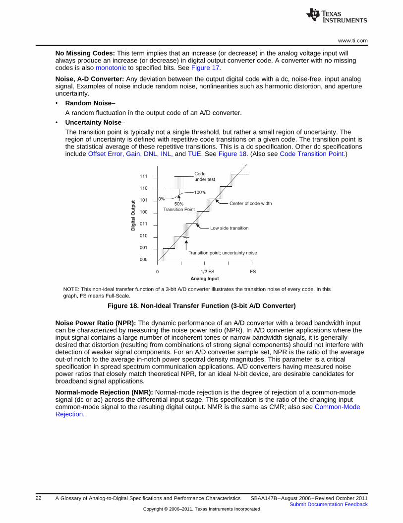
Noise, A-D Converter: Any deviation between the output digital code with a dc, noise-free, input analogsignal. Examples of noise include random noise, nonlinearities such as harmonic distortion, and apertureuncertainty.
• Random Noise–A random fluctuation in the output code of an A/D converter.
• Uncertainty Noise–The transition point is typically not a single threshold, but rather a small region of uncertainty. Theregion of uncertainty is defined with repetitive code transitions on a given code. The transition point isthe statistical average of these repetitive transitions. This is a dc specification. Other dc specificationsinclude Offset Error, Gain, DNL, INL, and TUE. See Figure 18. (Also see Code Transition Point.)
NOTE: This non-ideal transfer function of a 3-bit A/D converter illustrates the transition noise of every code. In thisgraph, FS means Full-Scale.
Figure 18. Non-Ideal Transfer Function (3-bit A/D Converter)
Noise Power Ratio (NPR): The dynamic performance of an A/D converter with a broad bandwidth inputcan be characterized by measuring the noise power ratio (NPR). In A/D converter applications where theinput signal contains a large number of incoherent tones or narrow bandwidth signals, it is generallydesired that distortion (resulting from combinations of strong signal components) should not interfere withdetection of weaker signal components. For an A/D converter sample set, NPR is the ratio of the averageout-of notch to the average in-notch power spectral density magnitudes. This parameter is a criticalspecification in spread spectrum communication applications. A/D converters having measured noisepower ratios that closely match theoretical NPR, for an ideal N-bit device, are desirable candidates forbroadband signal applications.
Normal-mode Rejection (NMR): Normal-mode rejection is the degree of rejection of a common-modesignal (dc or ac) across the differential input stage. This specification is the ratio of the changing inputcommon-mode signal to the resulting digital output. NMR is the same as CMR; also see Common-ModeRejection.
22 A Glossary of Analog-to-Digital Specifications and Performance Characteristics SBAA147B–August 2006–Revised October 2011Submit Documentation Feedback
Copyright © 2006–2011, Texas Instruments Incorporated
Offset Error = (V[0:1] (0.5)V )- ILSB
Actual
Transfer
Function
Ideal
Transfer
Function
Offset Error
Offset errors can be
corrected in software or
hardware.
000
Analog Input Voltage
001
010
011
100
101
110
111
Digital
Output
Code
FS1/2 FS 3/4 FS1/4 FS0
Offset Error = Difference
between the actual ( line)
first transition point and the
ideal ( line) first transition point.
dashed
solidFirst (Ideal)
Code
Transition
www.ti.com
Number of Converter Bits (n): The number of converter bits (n) represents the number of bits in theoutput digital word. The number of output codes that an A/D converter produces is 2n possible codes.
Nyquist Theorem: When sampling a signal at discrete intervals, this theorem postulates that theoretically,the sampling speed must be greater than twice the bandwidth of the input signal being sampled. TheNyquist frequency is half of the sample rate. When the signal bandwidth is less than half of the samplerate, the original signal can theoretically be reconstructed.
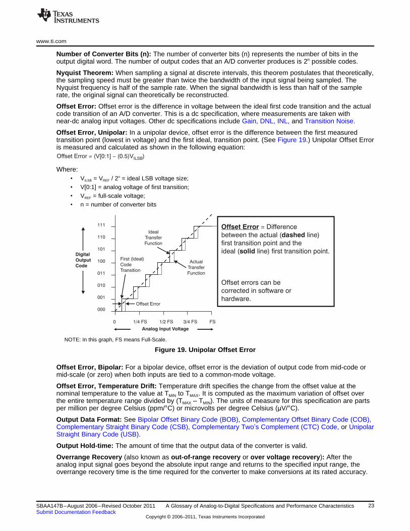
Offset Error: Offset error is the difference in voltage between the ideal first code transition and the actualcode transition of an A/D converter. This is a dc specification, where measurements are taken withnear-dc analog input voltages. Other dc specifications include Gain, DNL, INL, and Transition Noise.
Offset Error, Unipolar: In a unipolar device, offset error is the difference between the first measuredtransition point (lowest in voltage) and the first ideal, transition point. (See Figure 19.) Unipolar Offset Erroris measured and calculated as shown in the following equation:
Where:• VILSB = VREF / 2n = ideal LSB voltage size;• V[0:1] = analog voltage of first transition;• VREF = full-scale voltage;• n = number of converter bits
NOTE: In this graph, FS means Full-Scale.
Figure 19. Unipolar Offset Error
Offset Error, Bipolar: For a bipolar device, offset error is the deviation of output code from mid-code ormid-scale (or zero) when both inputs are tied to a common-mode voltage.
Offset Error, Temperature Drift: Temperature drift specifies the change from the offset value at thenominal temperature to the value at TMIN to TMAX. It is computed as the maximum variation of offset overthe entire temperature range divided by (TMAX – TMIN). The units of measure for this specification are partsper million per degree Celsius (ppm/°C) or microvolts per degree Celsius (μV/°C).
Output Data Format: See Bipolar Offset Binary Code (BOB), Complementary Offset Binary Code (COB),Complementary Straight Binary Code (CSB), Complementary Two’s Complement (CTC) Code, or UnipolarStraight Binary Code (USB).
Output Hold-time: The amount of time that the output data of the converter is valid.
Overrange Recovery (also known as out-of-range recovery or over voltage recovery): After theanalog input signal goes beyond the absolute input range and returns to the specified input range, theoverrange recovery time is the time required for the converter to make conversions at its rated accuracy.
23SBAA147B–August 2006–Revised October 2011 A Glossary of Analog-to-Digital Specifications and Performance CharacteristicsSubmit Documentation Feedback
Copyright © 2006–2011, Texas Instruments Incorporated
Passband Stop bandTransition
band
Frequency (Hz)
APASS
AMAX
ASTOP
Gain (dB)M = filter order
fCUT-OFF
fSTOP
e
www.ti.com
Oversampling: With an oversampling converter, the sample rate of the A/D converter is at a much higherfrequency than the converted analog frequency bandwidth. The Nyquist frequency fNYQUIST is:
fNYQUIST > 2 × fSIGNAL
where fSIGNAL is the highest frequency of interest in the input signal. The advantages of oversampling arethe lowering of the quantization noise contained within the passband, and moving harmonics out of theband of interest. Increasing the Oversampling Rate by two theoretically improves SNR by 3dB. UsingOversampling techniques makes anti-aliasing filter design easier. (Also see Nyquist Theorem.)
Passband: With an analog filter, the frequency span from dc to the analog cutoff frequency is defined asthe passband region. The magnitude of the response in the passband is defined as APASS, as shown inFigure 20. The response in the passband can be flat, with no ripple, as it is when an analog Butterworth orBessel filter is designed. Conversely, a Chebyshev filter has a ripple up to the cutoff frequency. Themagnitude of the ripple error of a filter is defined as ε.
Figure 20. Key Analog Filter Design Parameters
Parallel Interface: A parallel interface is where the A/D converter interface is capable of transferring morethan one bit simultaneously. The other type of A/D converter interface is a serial interface.
Phase Noise: Phase noise describes short-term, random frequency fluctuations (or time-based jitter) of aclock or input signal. Frequency stability is a measure of the degree to which an oscillator maintains thesame value of frequency over a given time. When phase noise is measured, it shows small variations inthe frequency phase angle with the signal magnitude constant. When observed on a spectrum analyzer,amplitude and phase noise appears as sideband noise on both sides of the carrier. Often, phase noisespecifications refer to single-sideband noise. Most phase noise measurement schemes fold bothsidebands together. Increased phase noise decreases the magnitude of SNR, degrading the overallconverter performance.
Phase Nonlinearity: Phase nonlinearity is the deviation of the phase response from a linear-phaseresponse as a function of frequency.
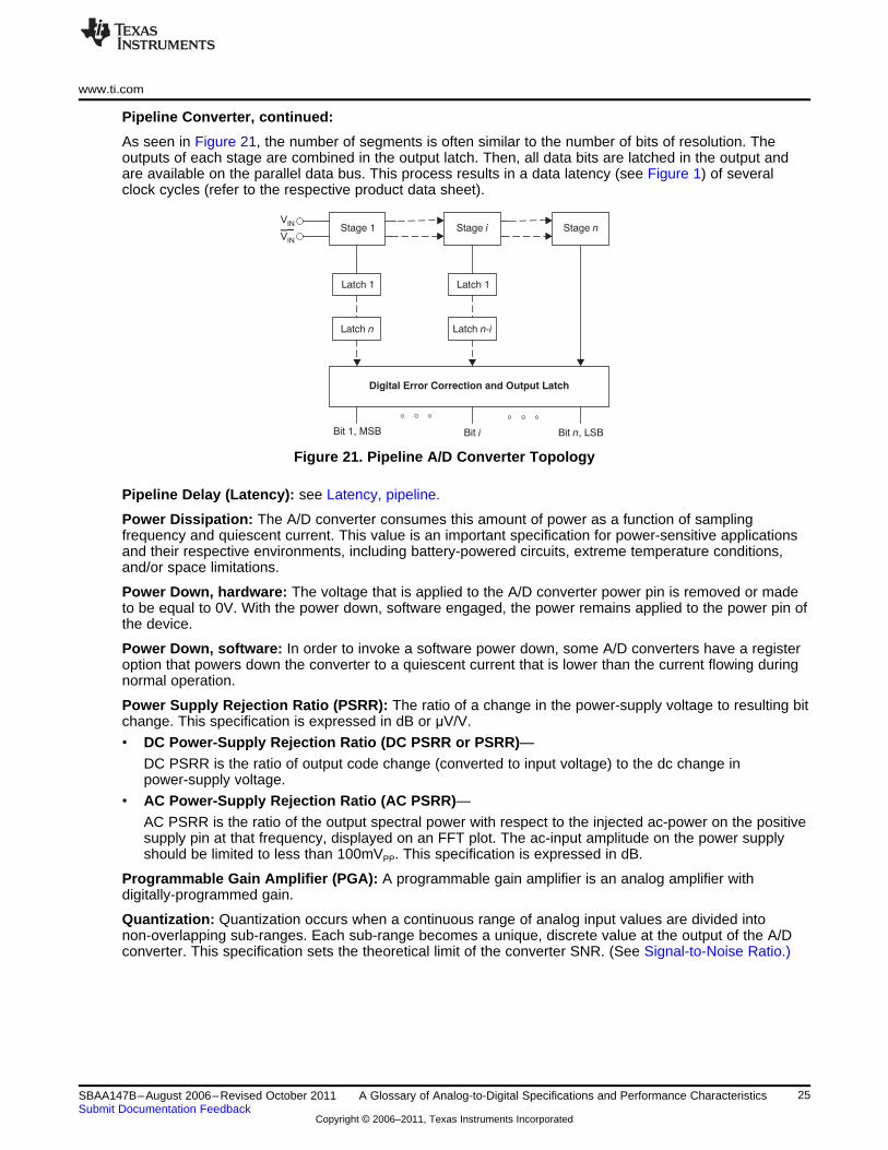
Pipeline Converter: A pipeline A/D converter consists of a number of consecutive segments. Eachsegment can execute its operation concurrently with other segments (see Figure 21). The segments aresimilar in their function and only resolve one or two bits. Each segment has a sample-and-hold, alow-resolution flash A/D converter, and a summing stage, including an inter-stage amplifier for providinggain. Stage 1 takes a sample of the input voltage and makes the first coarse conversion. The result is thenthe MSB and its digital value is fed to the first latch (Latch 1). When a segment completes an operation, itpasses the analog difference to the next segment. As the residue of the first stage gets resolved in thesubsequent n-stages, the MSB value ripples through the n number of latches in order to coincide with theend of the conversion of the last stage.
24 A Glossary of Analog-to-Digital Specifications and Performance Characteristics SBAA147B–August 2006–Revised October 2011Submit Documentation Feedback
Copyright © 2006–2011, Texas Instruments Incorporated
Stage 1 Stage i Stage nVIN
VIN
Latch 1 Latch 1
Latch n Latch n-i
Digital Error Correction and Output Latch
Bit 1, MSB Bit i Bit , LSBn
www.ti.com
Pipeline Converter, continued:
As seen in Figure 21, the number of segments is often similar to the number of bits of resolution. Theoutputs of each stage are combined in the output latch. Then, all data bits are latched in the output andare available on the parallel data bus. This process results in a data latency (see Figure 1) of severalclock cycles (refer to the respective product data sheet).
Figure 21. Pipeline A/D Converter Topology
Pipeline Delay (Latency): see Latency, pipeline.
Power Dissipation: The A/D converter consumes this amount of power as a function of samplingfrequency and quiescent current. This value is an important specification for power-sensitive applicationsand their respective environments, including battery-powered circuits, extreme temperature conditions,and/or space limitations.
Power Down, hardware: The voltage that is applied to the A/D converter power pin is removed or madeto be equal to 0V. With the power down, software engaged, the power remains applied to the power pin ofthe device.
Power Down, software: In order to invoke a software power down, some A/D converters have a registeroption that powers down the converter to a quiescent current that is lower than the current flowing duringnormal operation.
Power Supply Rejection Ratio (PSRR): The ratio of a change in the power-supply voltage to resulting bitchange. This specification is expressed in dB or μV/V.
• DC Power-Supply Rejection Ratio (DC PSRR or PSRR)—DC PSRR is the ratio of output code change (converted to input voltage) to the dc change inpower-supply voltage.
• AC Power-Supply Rejection Ratio (AC PSRR)—AC PSRR is the ratio of the output spectral power with respect to the injected ac-power on the positivesupply pin at that frequency, displayed on an FFT plot. The ac-input amplitude on the power supplyshould be limited to less than 100mVPP. This specification is expressed in dB.
Programmable Gain Amplifier (PGA): A programmable gain amplifier is an analog amplifier withdigitally-programmed gain.
Quantization: Quantization occurs when a continuous range of analog input values are divided intonon-overlapping sub-ranges. Each sub-range becomes a unique, discrete value at the output of the A/Dconverter. This specification sets the theoretical limit of the converter SNR. (See Signal-to-Noise Ratio.)
25SBAA147B–August 2006–Revised October 2011 A Glossary of Analog-to-Digital Specifications and Performance CharacteristicsSubmit Documentation Feedback
Copyright © 2006–2011, Texas Instruments Incorporated
Quantization Noise (rms) = =
(LSB)
2
3
±
12
q
www.ti.com
Quantization Noise: The noise that an A/D converter generates as a consequence of dividing the inputsignal into discrete buckets. The ideal width of these buckets is equal to the LSB size of the converter.The uncertainty of any A/D converter bit is ±1/2 LSB. This characterization is true for a perfect converterwith no Differential Non-Linearity (DNL) errors. If it is assumed the response of this error is a triangularacross an analog input signal, the rms value of the triangular signal is equal to the magnitude of signaldivided by the √3.
With:• q = ideal code width
Ratiometric Operation: This term describes an environment where the converter uses the samereference voltage as is used to drive the signal source, such as a sensor. Under these conditions, theoutput code is a function of the ratio of reference voltage to the signal source and is independent of thevalue of the reference voltage.
Record of Data: A record of data is a collection of samples that are acquired in a sequential fashion froman A/D converter.
Resolution: When describing the general performance of a converter, resolution is the number of possibleoutput bits that an A/D converter can produce in one conversion. Resolution also is the smallest analogincrement corresponding to a 1LSB converter change. This critical specification determines the smallestanalog input signal that can be resolved.
Rise Time: Rise time is the time required for a signal to rise from 10% of the transition range to 90% ofthat range.
Root-mean-square (rms): RMS is a mathematical term for the standard deviation from a record of data.The calculation of rms is equivalent to the square root of the arithmetic mean of the squared values (thedifference between the data and the mean).
Root-sum-square (rss): For a given set of data, rss is the square-root-of-the-sum-of-the-squares.
Sampling: Sampling assigns discrete time values to a continuous time signal.
Sample-and-Hold (or S&H): A sample-and-hold circuit has an analog-switched input with a function thatopens (samples) for a short duration to capture (hold) the analog input voltage.
Sampling Time: Sampling time is the time required to sample an analog input signal to a specified levelof accuracy. Also see Acquisition Time.
Sample Rate: The Sample Rate is the speed that a converter can continuously convert severalconversions. This critical specification determines the largest allowable bandwidth of the analog inputsignal. Typically specified as samples per second (sps) or hertz (Hz). (Also see Conversion MaximumRate.)
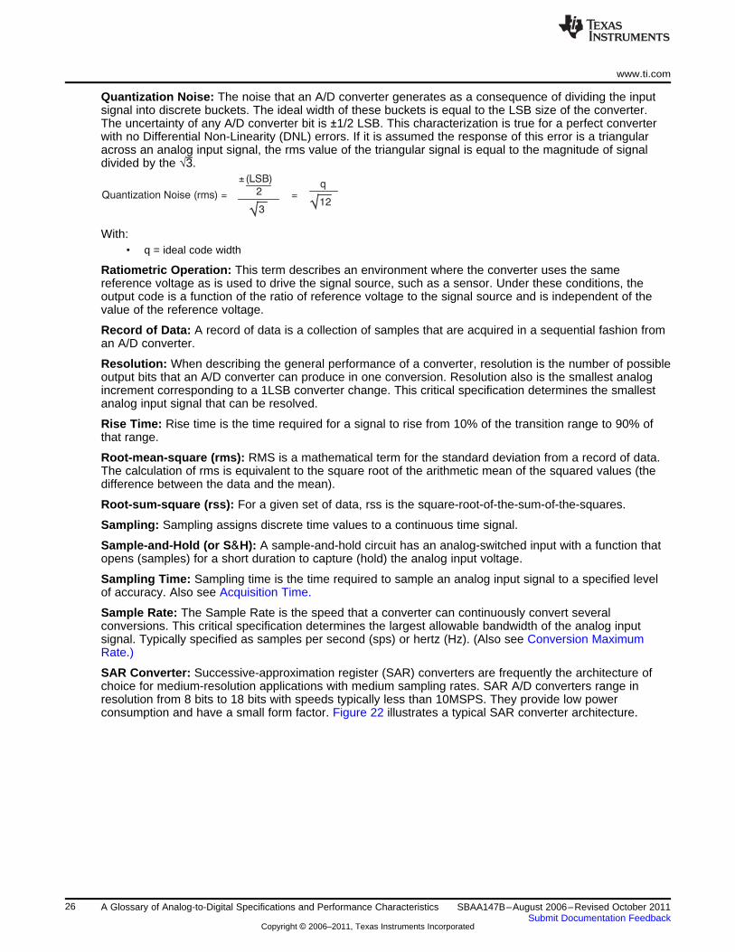
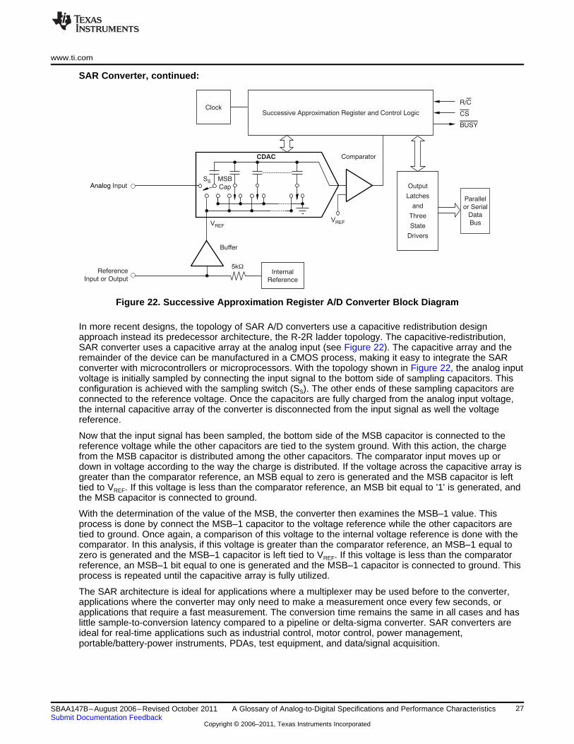
SAR Converter: Successive-approximation register (SAR) converters are frequently the architecture ofchoice for medium-resolution applications with medium sampling rates. SAR A/D converters range inresolution from 8 bits to 18 bits with speeds typically less than 10MSPS. They provide low powerconsumption and have a small form factor. Figure 22 illustrates a typical SAR converter architecture.
26 A Glossary of Analog-to-Digital Specifications and Performance Characteristics SBAA147B–August 2006–Revised October 2011Submit Documentation Feedback
Copyright © 2006–2011, Texas Instruments Incorporated
Buffer
Analog Input
Successive Approximation Register and Control LogicClock
Output
Latches
and
Three
State
Drivers
Comparator
Internal
Reference
5kWReference
Input or Output
CDAC
SS MSB
Cap
R/C
CS
BUSY
VREFVREF
Parallel
or Serial
Data
Bus
www.ti.com
SAR Converter, continued:
Figure 22. Successive Approximation Register A/D Converter Block Diagram
In more recent designs, the topology of SAR A/D converters use a capacitive redistribution designapproach instead its predecessor architecture, the R-2R ladder topology. The capacitive-redistribution,SAR converter uses a capacitive array at the analog input (see Figure 22). The capacitive array and theremainder of the device can be manufactured in a CMOS process, making it easy to integrate the SARconverter with microcontrollers or microprocessors. With the topology shown in Figure 22, the analog inputvoltage is initially sampled by connecting the input signal to the bottom side of sampling capacitors. Thisconfiguration is achieved with the sampling switch (SS). The other ends of these sampling capacitors areconnected to the reference voltage. Once the capacitors are fully charged from the analog input voltage,the internal capacitive array of the converter is disconnected from the input signal as well the voltagereference.
Now that the input signal has been sampled, the bottom side of the MSB capacitor is connected to thereference voltage while the other capacitors are tied to the system ground. With this action, the chargefrom the MSB capacitor is distributed among the other capacitors. The comparator input moves up ordown in voltage according to the way the charge is distributed. If the voltage across the capacitive array isgreater than the comparator reference, an MSB equal to zero is generated and the MSB capacitor is lefttied to VREF. If this voltage is less than the comparator reference, an MSB bit equal to '1' is generated, andthe MSB capacitor is connected to ground.
With the determination of the value of the MSB, the converter then examines the MSB–1 value. Thisprocess is done by connect the MSB–1 capacitor to the voltage reference while the other capacitors aretied to ground. Once again, a comparison of this voltage to the internal voltage reference is done with thecomparator. In this analysis, if this voltage is greater than the comparator reference, an MSB–1 equal tozero is generated and the MSB–1 capacitor is left tied to VREF. If this voltage is less than the comparatorreference, an MSB–1 bit equal to one is generated and the MSB–1 capacitor is connected to ground. Thisprocess is repeated until the capacitive array is fully utilized.
The SAR architecture is ideal for applications where a multiplexer may be used before to the converter,applications where the converter may only need to make a measurement once every few seconds, orapplications that require a fast measurement. The conversion time remains the same in all cases and haslittle sample-to-conversion latency compared to a pipeline or delta-sigma converter. SAR converters areideal for real-time applications such as industrial control, motor control, power management,portable/battery-power instruments, PDAs, test equipment, and data/signal acquisition.
27SBAA147B–August 2006–Revised October 2011 A Glossary of Analog-to-Digital Specifications and Performance CharacteristicsSubmit Documentation Feedback
Copyright © 2006–2011, Texas Instruments Incorporated
SNR (dB) = 10log10 S N, where P is the signal power and P is the noise power.P
PS
N
rms signal
rms noiseSNR (dB) = 10log10
SNR (dB) = 10log10ideal = 6.02n + 1.76 (dB)
(2(n - 1)
· )q
2
q
12
SINAD = 20log or- 10 (10 + 10 )-SNR/10 +THD/10
SINAD = 10log10
P
P + PS
N D
www.ti.com
Second Harmonic (HD2): The second harmonic is two times the frequency of the fundamental.
Settling Time (as it relates to ΔΣ A/D converters): The settling time of the digital filter in a delta-sigma A/Dconverter reflects the order of the digital filter internal to the converter. This time is given in cycles andequal to the number of conversions required for the signal to propagate through the filter. Settling time canbe an issue to consider after power-up, when switching channels with the input multiplexer, after an inputstep response, or re-starting the converter after a long wait time.
Signal-to-Noise Ratio (SNR): The signal-to-noise ratio is a calculated rms value that represents the ratioof ac signal power to noise power below one-half of the sampling frequency. The noise power excludesharmonic signals and dc.
The ideal SNR for SAR and pipeline converters with a full-scale sine wave input to an A/D converter is6.02n +1.76dB; n is equal to the number of converter bits. SNR can be specified with respect to full-scaleinput range (dBFS or dB) or with respect to the actual input signal amplitude (dBc). The three differentformulas for SNR are:
Where:• q = the LSB size• n = number of bits
The ideal SNR for a delta-sigma converter first-order modulator is 6.02n + 1.76dB + 10log10(fS / (2BW)),where fS is the converter sampling frequency and BW is the maximum frequency of interest.
Other dynamic or ac specifications include the Signal-to-Noise Ratio plus Distortion (SINAD or SNR+D),Effective Number Of Bits (ENOB), Total Harmonic Distortion (THD), Spurious Free Dynamic Range(SFDR), Intermodulation Distortion (IMD), and Full-power Bandwidth (FPBW). (Also see QuantizationNoise.)
Signal-to-(Noise Ratio plus Distortion) (SINAD or SNR+D, also called Total Harmonic Distortionplus Noise): SINAD is the calculated combination of SNR and total harmonic distortion (THD). SINAD isthe ratio of the rms amplitude of the fundamental input signal to the rms sum of all other spectralcomponents below one-half of the sampling frequency (excluding dc). The theoretical minimum for SINADis equal to the ideal SNR or 6.02n + 1.76dB with SAR and pipeline converters.
Where:• PS is the fundametal signal power;• PN is the power of all the noise spectral components; and• PD is the power of all the distortion spectral components
SINAD is either given in units of dBc (decibels to carrier) when the absolute power of the fundamental isused as the reference, or dBFS (decibels to full-scale) when the power of the fundamental is extrapolated
28 A Glossary of Analog-to-Digital Specifications and Performance Characteristics SBAA147B–August 2006–Revised October 2011Submit Documentation Feedback
Copyright © 2006–2011, Texas Instruments Incorporated
4kTRBThermal Resistor Noise =
www.ti.com
to the converter full-scale range. SINAD is a critical specification for digital oscilloscope/waveformrecorders, as well as geophysical, image processing, radar, sonar, spectrum analysis, video,telecommunication, and wideband digital receiver applications. Other dynamic or ac specifications includethe Signal-to-Noise Ratio (SNR),, Effective Number Of Bits (ENOB), Total Harmonic Distortion (THD),Intermodulation Distortion (IMD), and Full-power Bandwidth (FPBW).
Small Signal: A voltage input signal whose peak-to-peak amplitude spans not more than 10% of the fullinput range of the A/D converter.
Spurious Free Dynamic Range (SFDR): The distance in dB on an FFT plot from the fundamental inputsignal to the worst or highest spur. SFDR can be specified with respect to full-scale input range (dBFS ordB), or with respect to the actual input signal amplitude (dBc). (See Figure 23.) SFDR is a criticalspecification for telecommunication and video applications. Other dynamic or ac specifications include theSignal-to-Noise Ratio (SNR), Signal-to-Noise Ratio plus Distortion (SINAD or SNR+D), Effective NumberOf Bits (ENOB), Total Harmonic Distortion (THD), Intermodulation Distortion (IMD), and Full-powerBandwidth (FPBW).
Static Specifications: Static specifications are the A/D converter specifications pertaining to a dc signalinput. These specifications generally include Offset Error, Gain Error, DNL, INL, and TUE.
Step Response: The step response is the time required for the output digital results to reflect the ratedaccuracy of the converter after the input voltage goes from the lowest input voltage to the highest inputvoltage (or vice-versa).
SPI (Serial Peripheral Interface): See Digital Interface – SPI.
Successive Approximation Register Converter (SAR): See SAR Converter.
Synchronous Sampling: Synchronous sampling is where the input signal is phase locked to thesampling of another signal and/or to the A/D converter sampling frequency.
Temperature, Specified: The temperature range where electrical specifications apply. If the device istaken beyond the specified temperature range, the typical, maximum, and minimum specifications do notapply.
Temperature, Storage: The temperature range limiting storage conditions. If the device is stored attemperatures beyond the stated storage temperatures, damage to the device may occur.
Temperature, Junction: The maximum allowed internal junction temperature. If this junction temperatureis exceeded, the device may stop operation and/or damage may occur.
Temperature, Operating: The temperature range limits where the product continues to operate, but notnecessarily to specification.
Thermal Noise: Thermal Noise is generated by a resistor. Ideally, this noise is equal to:
Where:• k = Boltzmann's constant, 1.38 × 10⁻²³;• T = temperature in degrees Kelvin; and• B = bandwidth
Thermal Impedance: Thermal impedance quantifies a component or device capability to dissipate heat.In electronics, this heat is normally generated by the device power. With components, the overall thermalimpedance causes a rise in temperature that is linearly dependent on the power dissipated in the device.The coefficient is called θ, and has the units of °C/W.
Third Harmonic (HD3): The third harmonic is three times the frequency of the fundamental.
Throughput rate: Throughput rate is the inverse of throughput time.
Throughput Time: The time required for the converter to sample, acquire, digitize, and prepare for thenext conversion. This time is also the minimum conversion time in a continuous conversion application.
Timing Jitter: See Aperture Jitter.
Timing Phase Noise: See Aperture Jitter.
29SBAA147B–August 2006–Revised October 2011 A Glossary of Analog-to-Digital Specifications and Performance CharacteristicsSubmit Documentation Feedback
Copyright © 2006–2011, Texas Instruments Incorporated
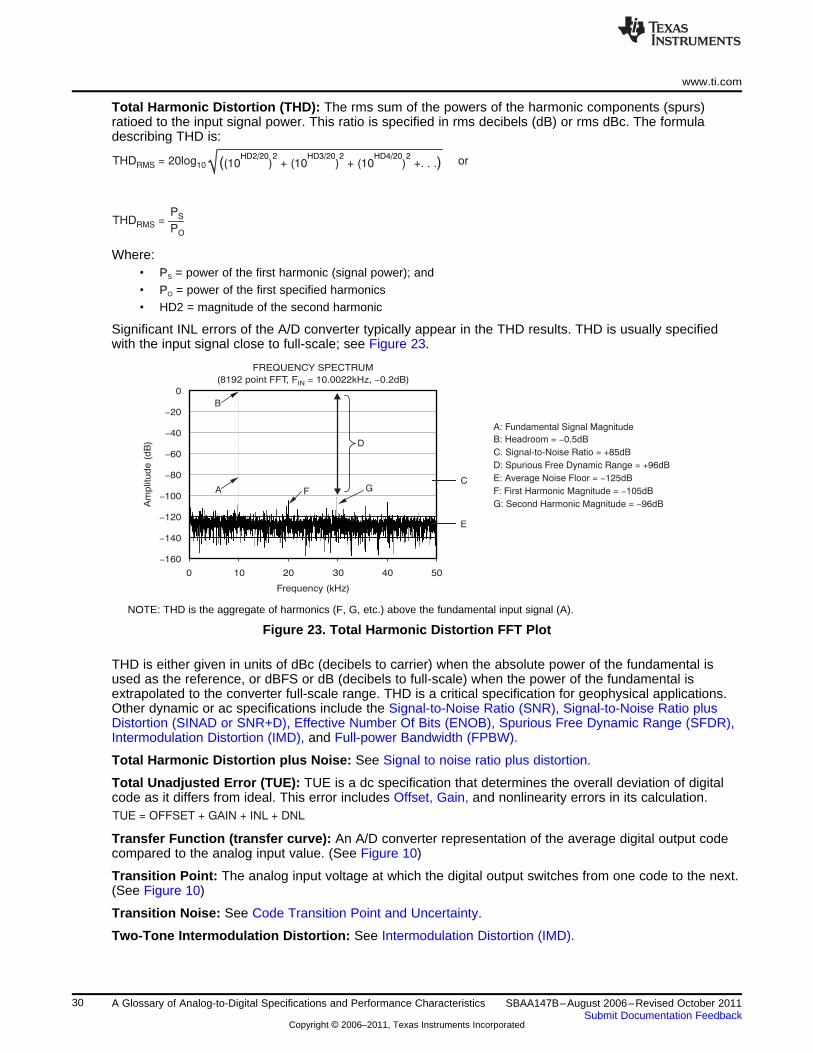
THDRMS 10= 20log or( )(10 ) + (10 ) + (10 ) +. . .HD2/20 2 HD3/20 2 HD4/20 2
THD =RMS
P
PS
O
A: Fundamental Signal Magnitude
B: Headroom = 0.5dB
C. Signal-to-Noise Ratio = 85dB
D: Spurious Free Dynamic Range = 96dB
E: Average Noise Floor = 125dB
F: First Harmonic Magnitude = 105dB
G: Second Harmonic Magnitude = 96dB
-
-
-
-
+
+
A
B
C
D
E
F G
0
-20
-40
-60
-80
-100
-120
-140
-160
Am
plit
ud
e (
dB
)
0 10 20 30 40 50
Frequency (kHz)
FREQUENCY SPECTRUM
(8192 point FFT, F = 10.0022kHz, 0.2dB)IN -
TUE = OFFSET + GAIN + INL + DNL
www.ti.com
Total Harmonic Distortion (THD): The rms sum of the powers of the harmonic components (spurs)ratioed to the input signal power. This ratio is specified in rms decibels (dB) or rms dBc. The formuladescribing THD is:
Where:• PS = power of the first harmonic (signal power); and• PO = power of the first specified harmonics• HD2 = magnitude of the second harmonic
Significant INL errors of the A/D converter typically appear in the THD results. THD is usually specifiedwith the input signal close to full-scale; see Figure 23.
NOTE: THD is the aggregate of harmonics (F, G, etc.) above the fundamental input signal (A).
Figure 23. Total Harmonic Distortion FFT Plot
THD is either given in units of dBc (decibels to carrier) when the absolute power of the fundamental isused as the reference, or dBFS or dB (decibels to full-scale) when the power of the fundamental isextrapolated to the converter full-scale range. THD is a critical specification for geophysical applications.Other dynamic or ac specifications include the Signal-to-Noise Ratio (SNR), Signal-to-Noise Ratio plusDistortion (SINAD or SNR+D), Effective Number Of Bits (ENOB), Spurious Free Dynamic Range (SFDR),Intermodulation Distortion (IMD), and Full-power Bandwidth (FPBW).
Total Harmonic Distortion plus Noise: See Signal to noise ratio plus distortion.
Total Unadjusted Error (TUE): TUE is a dc specification that determines the overall deviation of digitalcode as it differs from ideal. This error includes Offset, Gain, and nonlinearity errors in its calculation.
Transfer Function (transfer curve): An A/D converter representation of the average digital output codecompared to the analog input value. (See Figure 10)
Transition Point: The analog input voltage at which the digital output switches from one code to the next.(See Figure 10)
Transition Noise: See Code Transition Point and Uncertainty.
Two-Tone Intermodulation Distortion: See Intermodulation Distortion (IMD).
30 A Glossary of Analog-to-Digital Specifications and Performance Characteristics SBAA147B–August 2006–Revised October 2011Submit Documentation Feedback
Copyright © 2006–2011, Texas Instruments Incorporated
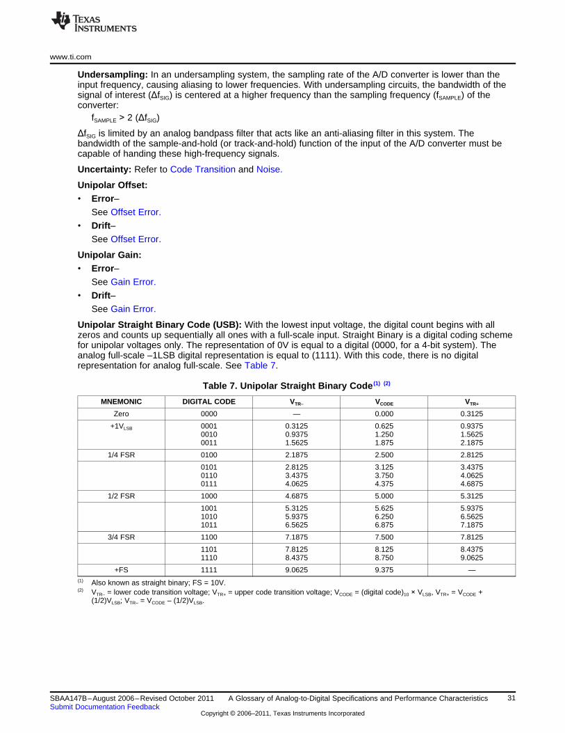
www.ti.com
Undersampling: In an undersampling system, the sampling rate of the A/D converter is lower than theinput frequency, causing aliasing to lower frequencies. With undersampling circuits, the bandwidth of thesignal of interest (ΔfSIG) is centered at a higher frequency than the sampling frequency (fSAMPLE) of theconverter:
fSAMPLE > 2 (ΔfSIG)
ΔfSIG is limited by an analog bandpass filter that acts like an anti-aliasing filter in this system. Thebandwidth of the sample-and-hold (or track-and-hold) function of the input of the A/D converter must becapable of handing these high-frequency signals.
Uncertainty: Refer to Code Transition and Noise.
Unipolar Offset:• Error–
See Offset Error.
• Drift–See Offset Error.
Unipolar Gain:• Error–
See Gain Error.
• Drift–See Gain Error.
Unipolar Straight Binary Code (USB): With the lowest input voltage, the digital count begins with allzeros and counts up sequentially all ones with a full-scale input. Straight Binary is a digital coding schemefor unipolar voltages only. The representation of 0V is equal to a digital (0000, for a 4-bit system). Theanalog full-scale –1LSB digital representation is equal to (1111). With this code, there is no digitalrepresentation for analog full-scale. See Table 7.
Table 7. Unipolar Straight Binary Code (1) (2)
MNEMONIC DIGITAL CODE VTR– VCODE VTR+
Zero 0000 — 0.000 0.3125
+1VLSB 0001 0.3125 0.625 0.93750010 0.9375 1.250 1.56250011 1.5625 1.875 2.1875
1/4 FSR 0100 2.1875 2.500 2.8125
0101 2.8125 3.125 3.43750110 3.4375 3.750 4.06250111 4.0625 4.375 4.6875
1/2 FSR 1000 4.6875 5.000 5.3125
1001 5.3125 5.625 5.93751010 5.9375 6.250 6.56251011 6.5625 6.875 7.1875
3/4 FSR 1100 7.1875 7.500 7.8125
1101 7.8125 8.125 8.43751110 8.4375 8.750 9.0625
+FS 1111 9.0625 9.375 —(1) Also known as straight binary; FS = 10V.(2) VTR– = lower code transition voltage; VTR+ = upper code transition voltage; VCODE = (digital code)10 × VLSB, VTR+ = VCODE +
(1/2)VLSB; VTR– = VCODE – (1/2)VLSB.
31SBAA147B–August 2006–Revised October 2011 A Glossary of Analog-to-Digital Specifications and Performance CharacteristicsSubmit Documentation Feedback
Copyright © 2006–2011, Texas Instruments Incorporated
Revision History www.ti.com
Voltage Reference (also know as Analog Voltage Reference): This reference voltage sets the analoginput range. For the actual analog input range for a given device, refer to the product data sheet. Thesource of this voltage can be internal or external to the A/D converter.
• Reference Error–The reference error is the variation of the actual reference voltage (VREFP – VREFM) or VREF from its idealvalue. The reference error is typically given as a percentage or absolute voltage.
Zero-Scale Error (or zero-code error): See Offset Error (Unipolar).
References
The following documents are available for download through the Texas Instruments web site(www.ti.com), except where noted.
• Albanus, J. (2000.). Coding schemes used with data converters. Application report SBAA042.
• Anonymous. (1995.) Understanding data converters. Application report SLAA013.
• Baker, B. (2005.). A Baker's Dozen: Real analog solutions for digital designers. Burlington, MA:Elsevier/Newnes.
• Institute of Electrical and Electronics Engineers, Inc. (2001.). IEEE STD-1241-2000: IEEE Standard forTerminology and Test Methods for Analog-to-Digital Converters. Available at IEEE.org.
• Oljaca, M. and Hendrick, T. (2004.). Data converters for industrial power measurement. Applicationreport SBAA117.
Revision History
Changes from A Revision (January, 2008) to B Revision .............................................................................................. Page
• Corrected mistake in units for dBm definition ....................................................................................... 13
NOTE: Page numbers for previous revisions may differ from page numbers in the current version.
32 Revision History SBAA147B–August 2006–Revised October 2011Submit Documentation Feedback
Copyright © 2006–2011, Texas Instruments Incorporated
IMPORTANT NOTICE
Texas Instruments Incorporated and its subsidiaries (TI) reserve the right to make corrections, modifications, enhancements, improvements,and other changes to its products and services at any time and to discontinue any product or service without notice. Customers shouldobtain the latest relevant information before placing orders and should verify that such information is current and complete. All products aresold subject to TI’s terms and conditions of sale supplied at the time of order acknowledgment.
TI warrants performance of its hardware products to the specifications applicable at the time of sale in accordance with TI’s standardwarranty. Testing and other quality control techniques are used to the extent TI deems necessary to support this warranty. Except wheremandated by government requirements, testing of all parameters of each product is not necessarily performed.
TI assumes no liability for applications assistance or customer product design. Customers are responsible for their products andapplications using TI components. To minimize the risks associated with customer products and applications, customers should provideadequate design and operating safeguards.
TI does not warrant or represent that any license, either express or implied, is granted under any TI patent right, copyright, mask work right,or other TI intellectual property right relating to any combination, machine, or process in which TI products or services are used. Informationpublished by TI regarding third-party products or services does not constitute a license from TI to use such products or services or awarranty or endorsement thereof. Use of such information may require a license from a third party under the patents or other intellectualproperty of the third party, or a license from TI under the patents or other intellectual property of TI.
Reproduction of TI information in TI data books or data sheets is permissible only if reproduction is without alteration and is accompaniedby all associated warranties, conditions, limitations, and notices. Reproduction of this information with alteration is an unfair and deceptivebusiness practice. TI is not responsible or liable for such altered documentation. Information of third parties may be subject to additionalrestrictions.
Resale of TI products or services with statements different from or beyond the parameters stated by TI for that product or service voids allexpress and any implied warranties for the associated TI product or service and is an unfair and deceptive business practice. TI is notresponsible or liable for any such statements.
TI products are not authorized for use in safety-critical applications (such as life support) where a failure of the TI product would reasonablybe expected to cause severe personal injury or death, unless officers of the parties have executed an agreement specifically governingsuch use. Buyers represent that they have all necessary expertise in the safety and regulatory ramifications of their applications, andacknowledge and agree that they are solely responsible for all legal, regulatory and safety-related requirements concerning their productsand any use of TI products in such safety-critical applications, notwithstanding any applications-related information or support that may beprovided by TI. Further, Buyers must fully indemnify TI and its representatives against any damages arising out of the use of TI products insuch safety-critical applications.
TI products are neither designed nor intended for use in military/aerospace applications or environments unless the TI products arespecifically designated by TI as military-grade or "enhanced plastic." Only products designated by TI as military-grade meet militaryspecifications. Buyers acknowledge and agree that any such use of TI products which TI has not designated as military-grade is solely atthe Buyer's risk, and that they are solely responsible for compliance with all legal and regulatory requirements in connection with such use.
TI products are neither designed nor intended for use in automotive applications or environments unless the specific TI products aredesignated by TI as compliant with ISO/TS 16949 requirements. Buyers acknowledge and agree that, if they use any non-designatedproducts in automotive applications, TI will not be responsible for any failure to meet such requirements.
Following are URLs where you can obtain information on other Texas Instruments products and application solutions:
Products Applications
Audio www.ti.com/audio Communications and Telecom www.ti.com/communications
Amplifiers amplifier.ti.com Computers and Peripherals www.ti.com/computers
Data Converters dataconverter.ti.com Consumer Electronics www.ti.com/consumer-apps
DLP® Products www.dlp.com Energy and Lighting www.ti.com/energy
DSP dsp.ti.com Industrial www.ti.com/industrial
Clocks and Timers www.ti.com/clocks Medical www.ti.com/medical
Interface interface.ti.com Security www.ti.com/security
Logic logic.ti.com Space, Avionics and Defense www.ti.com/space-avionics-defense
Power Mgmt power.ti.com Transportation and Automotive www.ti.com/automotive
Microcontrollers microcontroller.ti.com Video and Imaging www.ti.com/video
RFID www.ti-rfid.com
OMAP Mobile Processors www.ti.com/omap
Wireless Connectivity www.ti.com/wirelessconnectivity
TI E2E Community Home Page e2e.ti.com
Mailing Address: Texas Instruments, Post Office Box 655303, Dallas, Texas 75265Copyright © 2011, Texas Instruments Incorporated