Embed Size (px)
Citation preview
A fully nanoscopic dielectric laser
Günter Kewes,∗,† Rogelio Rodríguez-Oliveros,‡ Kathrin Höfner,‡ Alexander
Kuhlicke,† Oliver Benson,† and Kurt Busch‡,¶
Humboldt-Universität zu Berlin, Institut für Physik, AG Nanooptik, Newtonstr. 15, D-12489
Berlin, Germany, Humboldt-Universität zu Berlin, Institut für Physik, AG Theoretische Optik &
Photonik, Newtonstr. 15, D-12489 Berlin, Germany, and Max-Born Institut, Max-Born-Strasse
2a, D-12489 Berlin, Germany
E-mail: [email protected]
Abstract
In this article, we introduce the concept of a dielectric nanolaser that is nanoscopic in all
spatial dimensions. Our proposal is based on dielectric nanoparticles of high refractive index,
e.g., silicon, acting as a (passive) cavity (without intrinsic gain) that is decorated with a thin
film of organic gain media. Its resonance frequencies can be tuned over the entire visible range
and bright and dark modes can be addressed. So called ”magnetic” modes can be utilized,
which makes this dielectric nanolaser a complementary source of coherent nearfields similar
to the surface plasmon laser (which exploits electric modes). The small intrinsic losses in
silicon yield relatively high quality factors and low non-radiative decay rates of emitters close
to the cavity, both of which will lead to low thresholds. As we show in this work, the dielectric
nanolaser exhibits certain advantages relative to nanowire lasers and spasers, such as reduced
laser threshold, short switch-on times, size and design flexibility. The dielectric nanolaser is
∗To whom correspondence should be addressed†Humboldt-Universität zu Berlin, AG Nanooptik‡Humboldt-Universität zu Berlin, AG Theoretische Optik & Photonik¶Max-Born Institut, Max-Born-Strasse 2a, D-12489 Berlin, Germany
1
arX
iv:1
412.
4549
v2 [
phys
ics.
optic
s] 1
6 D
ec 2
014
compatible with standard lithographic fabrication approaches and its relative simple design
may allow for easy testing and realization of the concept. Thus, the silicon nanolaser might
soon find many applications in nanooptics and metamaterials.
Keywords: plasmonics, nanolaser, silicon
In order to achieve high integration densities for optoelectronic structures, research aims for
lasers to become smaller and smaller. For fully dielectric lasers a natural limit appeared to be
found, when semiconductor nanowire lasers were demonstrated.1–3 The concept of surface plas-
mon lasers (spasers) overcame this size limitation by utilizing plasmons instead of photons.4 While
the potential relevance of the spaser concept is out of question, as it could enable a plethora of ap-
plications in nanooptics5,6 and metamaterials,7 spasers suffer from high spasing/lasing thresholds
that could only be reduced when demanding fabrication requirements were employed.8 Further-
more, only few publications9,10 address the possibly most attractive design of fully nanoscopic
spaser structures that exploit localized plasmon modes in nanoparticles. Recently, it was even
questioned, that the spaser can provide any benefit with respect to other small lasers due to their
high thresholds.11
As we pointed out in our recently published theory for nanoscopic spasers,12 which is based
on fully electrodynamic (and analytic) Mie-theory, there are ways to significantly improve the
performance of spasers. However, the question arises, if there exist other and potentially more
feasible alternatives. Since our above theory allows not only the treatment of metallic spherical
plasmon-cavities but, in principle, any sphere supporting Mie-modes, we investigate, in this work,
spherical silicon nanoparticles as cavities. Specifically, we will show through a comparative study
of gold, silver and silicon cavities and their associated lasing performance, that certain aspects of
dielectric nanolasers based on silicon exhibit superior performance characteristics.
The heart of our nanolaser proposal is an improved resonator. Being well known for microwave
antenna designs, dielectric spheres have only recently been introduced as useful nanoantennas.13,14
In fact, silicon nanospheres support ”magnetic” (TE) and ”electric” (TM) Mie-modes over the
2
entire visible spectral range when the diameter is tuned from 100-200nm. As we will show, a
very thin layer of around 1nm of gain-medium, possibly deposited by the well-established layer-
by-layer approach,15 can provide sufficient gain for such a cavity to turn into a fully nanoscopic
laser.
Our model, briefly reviewed here, is a rate equation model for the photon number N and the
inversion DE :dDE
dt= NE(γp− γt)−DE(γp + γt +2X γMN) (1)
dNdt
= DE γM(N + 12)−
Re(ωres)
QN + 1
2 γMNE (2)
NE denotes the total number of two-level dipolar emitters that represent the gain medium here.
These emitters are assumed to be randomly oriented and homogeneously distributed over a thin
shell around the spherical particles. This realistic assumption enables us to derive an effective
single-mode rate equation model (eq. 1 and 2) that contains averaged decay rates γt (total decay
especially capturing lossy decay channels) and γM (actual decay into the active laser mode) for
the whole ensemble of emitters. γp denotes the overall excitation or pump rate assuming an equal
excitation for each emitter for simplicity. The parameters ωres and Q are the complex eigenfre-
quency and quality factor of the laser mode under investigation, respectively. X denotes the energy
degeneracy of that very eigenfrequency, the nth eigenfrequency will have a X(n)=2n+1 fold degen-
eracy (dipole: X=3; quadrupole X=5). In our calculations we assume only a single resonance with
distinct Q to give rise to a feedback (stimulated emission processes), whereas there are resonances
(with lower Q, higher degeneracy X and poorer spectral overlap to the emitters) that very well lead
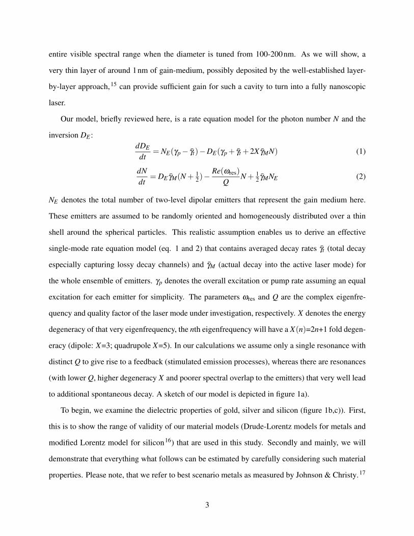
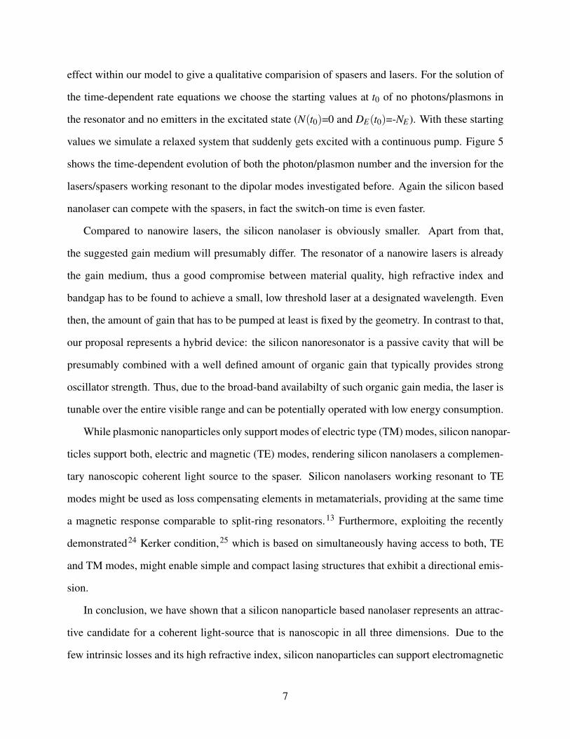
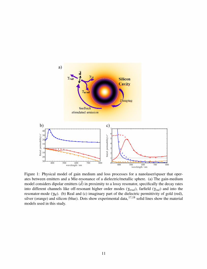
to additional spontaneous decay. A sketch of our model is depicted in figure 1a).
To begin, we examine the dielectric properties of gold, silver and silicon (figure 1b,c)). First,
this is to show the range of validity of our material models (Drude-Lorentz models for metals and
modified Lorentz model for silicon16) that are used in this study. Secondly and mainly, we will
demonstrate that everything what follows can be estimated by carefully considering such material
properties. Please note, that we refer to best scenario metals as measured by Johnson & Christy.17
3
For silicon we use data measured by Aspnes18 whereas others found even smaller extinction coef-
ficients.19 This underlines that the following results represent a conservative estimate. From figure
1b) it can be seen, that the real part of silicon’s relative permittivity ε ′ and thus its refractive index
nr is rather large for frequencies in the optical regime, roughly nr=4, meaning that the wavelength
of light is four times shorter in this medium so that localized modes will also be of smaller ex-
tent. Furthermore the imaginary part ε ′′ is surprisingly small even though silicons bandgap is only
1.1eV wide. This is due to the indirect bandgap of silicon and explains the observation of rela-
tively high-quality resonances at photon energies above 1.1eV. The imaginary part of the relative
permittivity ε ′′ (ε ′′=2nrκ) is the relevant number when silver and gold are compared to silicon.
Silicon exhibits an extinction coefficient κ that is orders of magnitude lower but electromagnetic
fields will more efficiently penetrate the dielectric material due to its high refractive index leading
to higher overall losses as it would be inferred by κ alone. However, in terms of ε ′′ silicon is still
as good as the best plasmonic metal silver (except for the ultraviolet (UV) part of the spectrum)
and consequently better than gold.
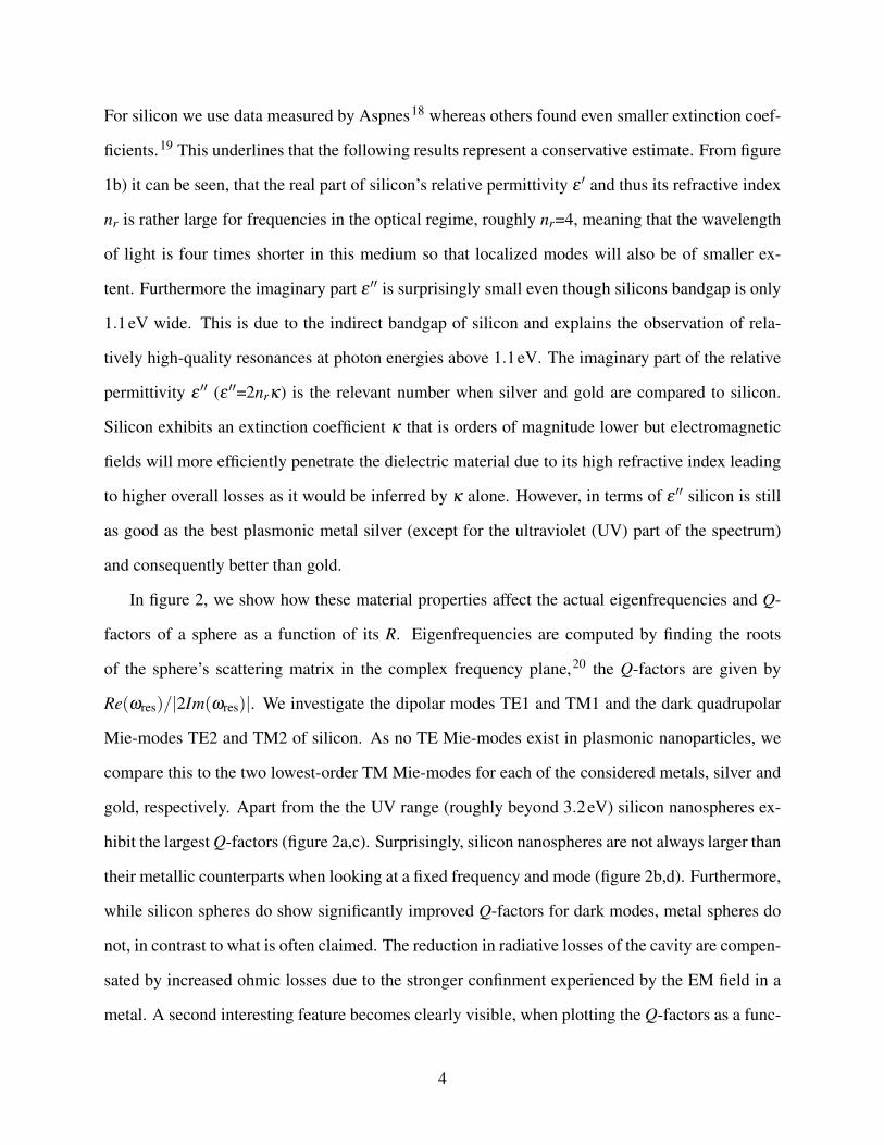
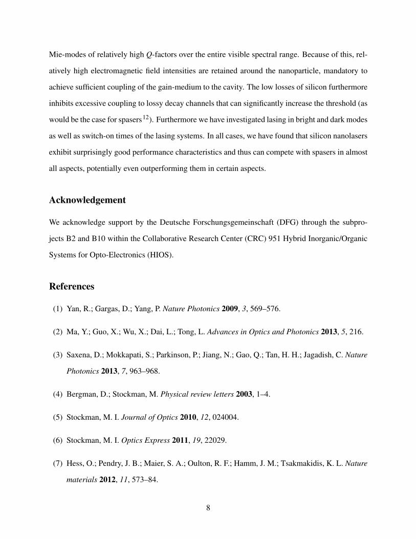
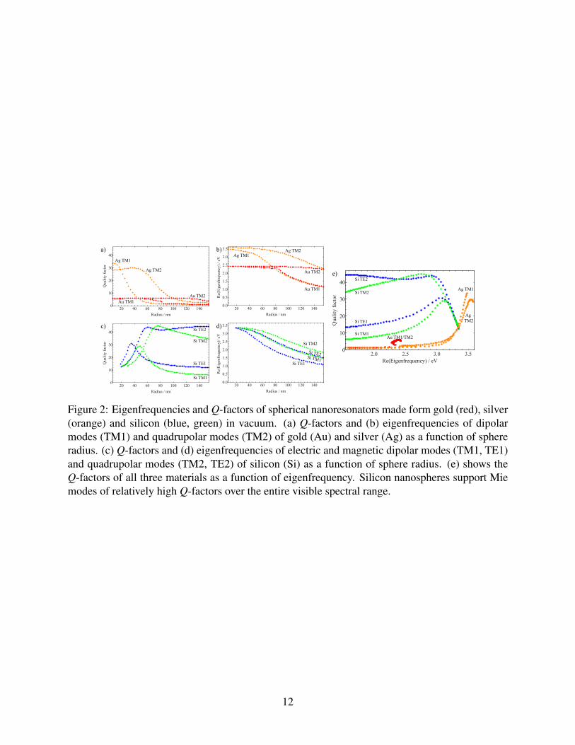
In figure 2, we show how these material properties affect the actual eigenfrequencies and Q-
factors of a sphere as a function of its R. Eigenfrequencies are computed by finding the roots
of the sphere’s scattering matrix in the complex frequency plane,20 the Q-factors are given by
Re(ωres)/|2Im(ωres)|. We investigate the dipolar modes TE1 and TM1 and the dark quadrupolar
Mie-modes TE2 and TM2 of silicon. As no TE Mie-modes exist in plasmonic nanoparticles, we
compare this to the two lowest-order TM Mie-modes for each of the considered metals, silver and
gold, respectively. Apart from the the UV range (roughly beyond 3.2eV) silicon nanospheres ex-
hibit the largest Q-factors (figure 2a,c). Surprisingly, silicon nanospheres are not always larger than
their metallic counterparts when looking at a fixed frequency and mode (figure 2b,d). Furthermore,
while silicon spheres do show significantly improved Q-factors for dark modes, metal spheres do
not, in contrast to what is often claimed. The reduction in radiative losses of the cavity are compen-
sated by increased ohmic losses due to the stronger confinment experienced by the EM field in a
metal. A second interesting feature becomes clearly visible, when plotting the Q-factors as a func-
4
tion of their eigenfrequencies. Silicon nanosphere resonances span the entire visible range while
at the same time preserving their high Q-factors (figure 2e). In contrast, metallic nanospheres with
reasonable Q-factors are limited to a rather tight spectral range. It is well known that nanorods ex-
hibit larger Q-factors than spheres (up to approximately 20 for gold) also at longer wavelengths.21
However, little is known about such beneficial effects on the Q-factors of dark modes. Also it is
beyond the scope of this paper to investigate different shapes of silicon nanoparticles to find bet-
ter Q-factors. In any case, silicon particles can reach high Q-factors over the entire visible range
already with the simplest design, a sphere.
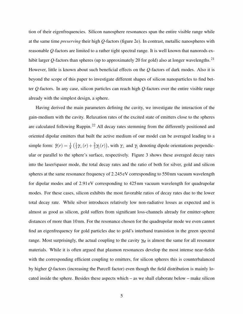
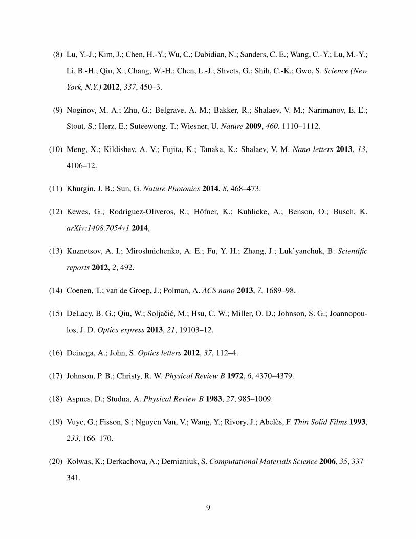
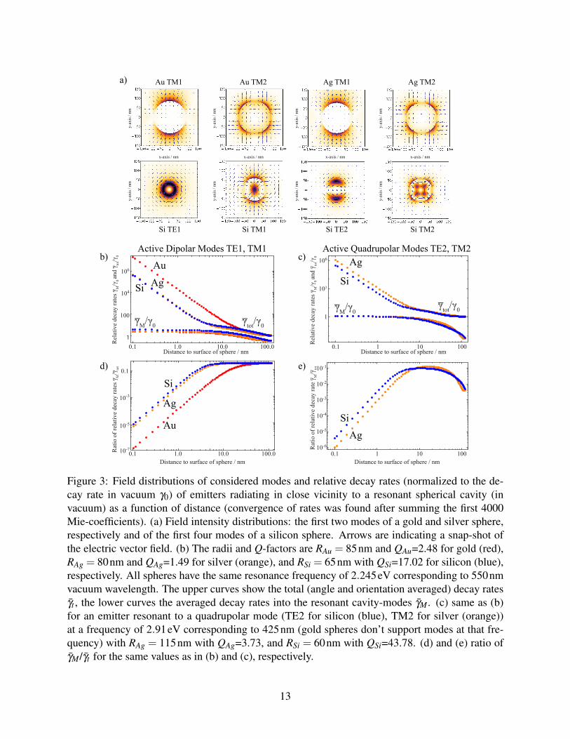
Having derived the main parameters defining the cavity, we investigate the interaction of the
gain-medium with the cavity. Relaxation rates of the excited state of emitters close to the spheres
are calculated following Ruppin.22 All decay rates stemming from the differently positioned and
oriented dipolar emitters that built the active medium of our model can be averaged leading to a
simple form: γ(r) = 1X
(13γ⊥(r)+ 2
3γ‖(r)), with γ⊥ and γ‖ denoting dipole orientations perpendic-
ular or parallel to the sphere’s surface, respectively. Figure 3 shows these averaged decay rates
into the laser/spaser mode, the total decay rates and the ratio of both for silver, gold and silicon
spheres at the same resonance frequency of 2.245eV corresponding to 550nm vacuum wavelength
for dipolar modes and of 2.91eV corresponding to 425nm vacuum wavelength for quadrupolar
modes. For these cases, silicon exhibits the most favorable ratios of decay rates due to the lower
total decay rate. While silver introduces relatively low non-radiative losses as expected and is
almost as good as silicon, gold suffers from significant loss-channels already for emitter-sphere
distances of more than 10nm. For the resonance chosen for the quadrupolar mode we even cannot
find an eigenfrequency for gold particles due to gold’s interband transistion in the green spectral
range. Most surprisingly, the actual coupling to the cavity γM is almost the same for all resonator
materials. While it is often argued that plasmon resonances develop the most intense near-fields
with the corresponding efficient coupling to emitters, for silicon spheres this is counterbalanced
by higher Q-factors (increasing the Purcell factor) even though the field distribution is mainly lo-
cated inside the sphere. Besides these aspects which – as we shall elaborate below – make silicon
5
nanospheres very attractive for nanolaser applications on principal grounds, we would like to also
discuss a number of practical aspects related to silicon nanocavities. Clearly, silicon is one of the
best studied materials and can be fabricated with highest quality using well established techniques.
For instance, a thin emitter-free spacing layer between gain-medium and cavity, which will sig-
nificantly lower the threshold of the nanolaser,12 can very easily be implemented as silicondioxid
films of around 1nm and thicker, grown in a well-controlled manner via thermal oxidation.23 Fur-
ther, spherical silicon nanoparticles can straightforwardly be synthesized, e.g., from the gas phase
– however, not yet with mono-disperse size distributions as would be required for direct appli-
cation in nanolasers. Therefore, appropriate filter-techniques have to be applied to obtain silicon
nanoparticles with sufficiently narrow size distributions. Alternatively, the fabrication of appropri-
ate nanostructures via e-beam lithography on silicon-on-insulator chips is straightforward and has
already been demonstrated.14
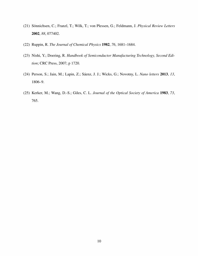
So far, we have found that Q-factors are best for silicon nanospheres, that unwanted non-
radiative decay-rates close to the sphere are relatively small, especially smaller than for the metall
spheres and that the decay rate into the cavity is of comparable magnitude. As alluded to above,
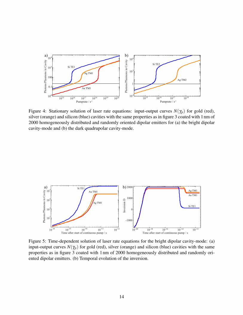
this already implies that the silicon nanolaser exhibits excellent performance characteristics, also
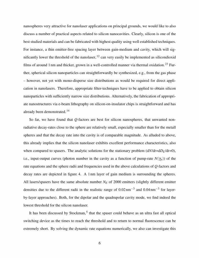
when compared to spasers. The analytic solutions for the stationary problem (dN/dt=dDE /dt=0),
i.e., input-output curves (photon number in the cavity as a function of pump-rate N(γp)) of the
rate equations and the sphere radii and frequencies used in the above calculations of Q-factors and
decay rates are depicted in figure 4. A 1nm layer of gain medium is surrounding the spheres.
All lasers/spasers have the same absolute number NE of 2000 emitters (slightly different emitter
densities due to the different radii in the realistic range of 0.02nm−3 and 0.04nm−3 for layer-
by-layer approaches). Both, for the dipolar and the quadrupolar cavity mode, we find indeed the
lowest threshold for the silicon nanolaser.
It has been discussed by Stockman,5 that the spaser could behave as an ultra fast all optical
switching device as the times to reach the threshold and to return to normal fluorescence can be
extremely short. By solving the dynamic rate equations numerically, we also can investigate this
6
effect within our model to give a qualitative comparision of spasers and lasers. For the solution of
the time-dependent rate equations we choose the starting values at t0 of no photons/plasmons in
the resonator and no emitters in the excitated state (N(t0)=0 and DE(t0)=-NE). With these starting
values we simulate a relaxed system that suddenly gets excited with a continuous pump. Figure 5
shows the time-dependent evolution of both the photon/plasmon number and the inversion for the
lasers/spasers working resonant to the dipolar modes investigated before. Again the silicon based
nanolaser can compete with the spasers, in fact the switch-on time is even faster.
Compared to nanowire lasers, the silicon nanolaser is obviously smaller. Apart from that,
the suggested gain medium will presumably differ. The resonator of a nanowire lasers is already
the gain medium, thus a good compromise between material quality, high refractive index and
bandgap has to be found to achieve a small, low threshold laser at a designated wavelength. Even
then, the amount of gain that has to be pumped at least is fixed by the geometry. In contrast to that,
our proposal represents a hybrid device: the silicon nanoresonator is a passive cavity that will be
presumably combined with a well defined amount of organic gain that typically provides strong
oscillator strength. Thus, due to the broad-band availabilty of such organic gain media, the laser is
tunable over the entire visible range and can be potentially operated with low energy consumption.
While plasmonic nanoparticles only support modes of electric type (TM) modes, silicon nanopar-
ticles support both, electric and magnetic (TE) modes, rendering silicon nanolasers a complemen-
tary nanoscopic coherent light source to the spaser. Silicon nanolasers working resonant to TE
modes might be used as loss compensating elements in metamaterials, providing at the same time
a magnetic response comparable to split-ring resonators.13 Furthermore, exploiting the recently
demonstrated24 Kerker condition,25 which is based on simultaneously having access to both, TE
and TM modes, might enable simple and compact lasing structures that exhibit a directional emis-
sion.
In conclusion, we have shown that a silicon nanoparticle based nanolaser represents an attrac-
tive candidate for a coherent light-source that is nanoscopic in all three dimensions. Due to the
few intrinsic losses and its high refractive index, silicon nanoparticles can support electromagnetic
7
Mie-modes of relatively high Q-factors over the entire visible spectral range. Because of this, rel-
atively high electromagnetic field intensities are retained around the nanoparticle, mandatory to
achieve sufficient coupling of the gain-medium to the cavity. The low losses of silicon furthermore
inhibits excessive coupling to lossy decay channels that can significantly increase the threshold (as
would be the case for spasers12). Furthermore we have investigated lasing in bright and dark modes
as well as switch-on times of the lasing systems. In all cases, we have found that silicon nanolasers
exhibit surprisingly good performance characteristics and thus can compete with spasers in almost
all aspects, potentially even outperforming them in certain aspects.
Acknowledgement
We acknowledge support by the Deutsche Forschungsgemeinschaft (DFG) through the subpro-
jects B2 and B10 within the Collaborative Research Center (CRC) 951 Hybrid Inorganic/Organic
Systems for Opto-Electronics (HIOS).
References
(1) Yan, R.; Gargas, D.; Yang, P. Nature Photonics 2009, 3, 569–576.
(2) Ma, Y.; Guo, X.; Wu, X.; Dai, L.; Tong, L. Advances in Optics and Photonics 2013, 5, 216.
(3) Saxena, D.; Mokkapati, S.; Parkinson, P.; Jiang, N.; Gao, Q.; Tan, H. H.; Jagadish, C. Nature
Photonics 2013, 7, 963–968.
(4) Bergman, D.; Stockman, M. Physical review letters 2003, 1–4.
(5) Stockman, M. I. Journal of Optics 2010, 12, 024004.
(6) Stockman, M. I. Optics Express 2011, 19, 22029.
(7) Hess, O.; Pendry, J. B.; Maier, S. A.; Oulton, R. F.; Hamm, J. M.; Tsakmakidis, K. L. Nature
materials 2012, 11, 573–84.
8
(8) Lu, Y.-J.; Kim, J.; Chen, H.-Y.; Wu, C.; Dabidian, N.; Sanders, C. E.; Wang, C.-Y.; Lu, M.-Y.;
Li, B.-H.; Qiu, X.; Chang, W.-H.; Chen, L.-J.; Shvets, G.; Shih, C.-K.; Gwo, S. Science (New
York, N.Y.) 2012, 337, 450–3.
(9) Noginov, M. A.; Zhu, G.; Belgrave, A. M.; Bakker, R.; Shalaev, V. M.; Narimanov, E. E.;
Stout, S.; Herz, E.; Suteewong, T.; Wiesner, U. Nature 2009, 460, 1110–1112.
(10) Meng, X.; Kildishev, A. V.; Fujita, K.; Tanaka, K.; Shalaev, V. M. Nano letters 2013, 13,
4106–12.
(11) Khurgin, J. B.; Sun, G. Nature Photonics 2014, 8, 468–473.
(12) Kewes, G.; Rodríguez-Oliveros, R.; Höfner, K.; Kuhlicke, A.; Benson, O.; Busch, K.
arXiv:1408.7054v1 2014,
(13) Kuznetsov, A. I.; Miroshnichenko, A. E.; Fu, Y. H.; Zhang, J.; Luk’yanchuk, B. Scientific
reports 2012, 2, 492.
(14) Coenen, T.; van de Groep, J.; Polman, A. ACS nano 2013, 7, 1689–98.
(15) DeLacy, B. G.; Qiu, W.; Soljacic, M.; Hsu, C. W.; Miller, O. D.; Johnson, S. G.; Joannopou-
los, J. D. Optics express 2013, 21, 19103–12.
(16) Deinega, A.; John, S. Optics letters 2012, 37, 112–4.
(17) Johnson, P. B.; Christy, R. W. Physical Review B 1972, 6, 4370–4379.
(18) Aspnes, D.; Studna, A. Physical Review B 1983, 27, 985–1009.
(19) Vuye, G.; Fisson, S.; Nguyen Van, V.; Wang, Y.; Rivory, J.; Abelès, F. Thin Solid Films 1993,
233, 166–170.
(20) Kolwas, K.; Derkachova, A.; Demianiuk, S. Computational Materials Science 2006, 35, 337–
341.
9
(21) Sönnichsen, C.; Franzl, T.; Wilk, T.; von Plessen, G.; Feldmann, J. Physical Review Letters
2002, 88, 077402.
(22) Ruppin, R. The Journal of Chemical Physics 1982, 76, 1681–1684.
(23) Nishi, Y.; Doering, R. Handbook of Semiconductor Manufacturing Technology, Second Edi-
tion; CRC Press, 2007; p 1720.
(24) Person, S.; Jain, M.; Lapin, Z.; Sáenz, J. J.; Wicks, G.; Novotny, L. Nano letters 2013, 13,
1806–9.
(25) Kerker, M.; Wang, D.-S.; Giles, C. L. Journal of the Optical Society of America 1983, 73,
765.
10
b) c)
a)
400 500 600 700 8000
1
2
3
4
5
6
7
wavelength / nm
Im(r
el. p
erm
eabi
lity)
ε“
400 500 600 700 80030
20
10
0
10
20
30
40
wavelength / nm
Re(
rel.
perm
eabi
lity)
ε‘
Figure 1: Physical model of gain medium and loss processes for a nanolaser/spaser that oper-ates between emitters and a Mie-resonance of a dielectric/metallic sphere. (a) The gain-mediummodel considers dipolar emitters (~d) in proximity to a lossy resonator, specifically the decay ratesinto different channels like off-resonant higher order modes (γnrad), farfield (γrad) and into theresonator-mode (γM). (b) Real and (c) imaginary part of the dielectric permittivity of gold (red),silver (orange) and silicon (blue). Dots show experimental data,17,18 solid lines show the materialmodels used in this study.
11
20 40 60 80 100 120 1400
10
20
30
40
Radius / nm
Qua
lity
fact
or
a) b)
c) d)
e)
20 40 60 80 100 120 1400
10
20
30
40
Radius / nm
Qua
lity
fact
or
2.0 2.5 3.0 3.50
10
20
30
40
Re(Eigenfrequency) / eV
Qua
lity
fact
or
20 40 60 80 100 120 1400.0
0.5
1.0
1.5
2.0
2.5
3.0
3.5
Radius / nm
Re(
Eige
nfre
quen
cy) /
eV
20 40 60 80 100 120 1400.0
0.5
1.0
1.5
2.0
2.5
3.0
3.5
Radius / nm
Re(
Eige
nfre
quen
cy)/
eV
Si TE1
Au TM2
Ag TM1
Ag TM2
Au TM1
Si TM1
Si TM2
Si TE2
Si TE1
Si TE2Si TM1
Si TM2
Si TE1
Si TM1
Si TM2
Si TE2
Ag TM2
Ag TM1
Au TM1/TM2
Ag TM2Ag TM1
Au TM2
Au TM1
Figure 2: Eigenfrequencies and Q-factors of spherical nanoresonators made form gold (red), silver(orange) and silicon (blue, green) in vacuum. (a) Q-factors and (b) eigenfrequencies of dipolarmodes (TM1) and quadrupolar modes (TM2) of gold (Au) and silver (Ag) as a function of sphereradius. (c) Q-factors and (d) eigenfrequencies of electric and magnetic dipolar modes (TM1, TE1)and quadrupolar modes (TM2, TE2) of silicon (Si) as a function of sphere radius. (e) shows theQ-factors of all three materials as a function of eigenfrequency. Silicon nanospheres support Miemodes of relatively high Q-factors over the entire visible spectral range.
12
Distance to surface of sphere / nm
Rel
ativ
e de
cay
rate
s γM
/γ0 an
d γ to
t/γ0
0.1 1 10 100
1
103
106
Rel
ativ
e de
cay
rate
s γM
/γ0 an
d γ to
t/γ0
Distance to surface of sphere / nm
Rat
io o
f rel
ativ
e de
cay
rate
s γM
/γto
t
Distance to surface of sphere / nm0.1 1 10 100
10-6
10-5
10-4
10-3
10-2
10-1
Distance to surface of sphere / nm
Rat
io o
f rel
ativ
e de
cay
rate
γM
/γto
t
b) c)
d) e)
Si
Ag
SiAg
__
__
__
__
Au TM1 Au TM2 Ag TM1 Ag TM2
Si TE1 Si TM1 Si TE2 Si TM2
a)
0.1 1.0 10.0 100.0
0.1
10-7
-5
10
10
-3
0.1 1.0 10.0 100.01
100
104
106
x-axis / nm x-axis / nm x-axis / nm x-axis / nm
y-ax
is /
nmy-
axis
/ nm
y-ax
is /
nmy-
axis
/ nm
y-ax
is /
nmy-
axis
/ nm
y-ax
is /
nmy-
axis
/ nm
Si Ag
Au
Si
Ag
Au
Active Dipolar Modes TE1, TM1 Active Quadrupolar Modes TE2, TM2
γM/γ0_
γM/γ0_
γtot/γ0_
γtot/γ0_
Figure 3: Field distributions of considered modes and relative decay rates (normalized to the de-cay rate in vacuum γ0) of emitters radiating in close vicinity to a resonant spherical cavity (invacuum) as a function of distance (convergence of rates was found after summing the first 4000Mie-coefficients). (a) Field intensity distributions: the first two modes of a gold and silver sphere,respectively and of the first four modes of a silicon sphere. Arrows are indicating a snap-shot ofthe electric vector field. (b) The radii and Q-factors are RAu = 85nm and QAu=2.48 for gold (red),RAg = 80nm and QAg=1.49 for silver (orange), and RSi = 65nm with QSi=17.02 for silicon (blue),respectively. All spheres have the same resonance frequency of 2.245eV corresponding to 550nmvacuum wavelength. The upper curves show the total (angle and orientation averaged) decay ratesγt , the lower curves the averaged decay rates into the resonant cavity-modes γM. (c) same as (b)for an emitter resonant to a quadrupolar mode (TE2 for silicon (blue), TM2 for silver (orange))at a frequency of 2.91eV corresponding to 425nm (gold spheres don’t support modes at that fre-quency) with RAg = 115nm with QAg=3.73, and RSi = 60nm with QSi=43.78. (d) and (e) ratio ofγM/γt for the same values as in (b) and (c), respectively.
13
Pumprate / s-1
Phot
ons/
Plas
mon
s in
Cav
ity
Au TM1
Ag TM1
Si TE1
Ag TM2
Si TE2
a) b)
Phot
ons/
Plas
mon
s in
Cav
ity
1015 1016 1017 1018 1019 102010
0.1
100
10 5
10 8
-4
Pumprate / s-11015 1016 1017 101810-3
10
106
1
3
Figure 4: Stationary solution of laser rate equations: input-output curves N(γp) for gold (red),silver (orange) and silicon (blue) cavities with the same properties as in figure 3 coated with 1nm of2000 homogeneously distributed and randomly oriented dipolar emitters for (a) the bright dipolarcavity-mode and (b) the dark quadrupolar cavity-mode.
Ag TM1
Si TE1
Au TM1
Ag TM1
Si TE1Au TM1
a) b)
Time after start of contineous pump / s
Phot
ons/
Plas
mon
s in
Cav
ity
10-16 10-15 10-14 10-13 10-12
10
107
105
103
1
10-20 10-18 10-16 10-14 10-12
Time after start of contineous pump / s
Inve
rsio
nD
-1000
0
1000
2000
Figure 5: Time-dependent solution of laser rate equations for the bright dipolar cavity-mode: (a)input-output curves N(γp) for gold (red), silver (orange) and silicon (blue) cavities with the sameproperties as in figure 3 coated with 1nm of 2000 homogeneously distributed and randomly ori-ented dipolar emitters. (b) Temporal evolution of the inversion.
14