Embed Size (px)
Citation preview
Progress In Electromagnetics Research B, Vol. 51, 307–328, 2013
A FREE-SPACE METHOD FOR COMPLEX PERMITTIV-ITY MEASUREMENT OF BULK AND THIN FILM DI-ELECTRICS AT MICROWAVE FREQUENCIES
Zaiki Awang*, Fatimah A. M. Zaki, Noor H. Baba,Ahmad S. Zoolfakar, and Raudah A. Bakar
Microwave Technology Centre, Universiti Teknologi MARA, ShahAlam 40450, Malaysia
Abstract—A free-space, non-destructive method for measuring thecomplex permittivity of a double-layer bulk dielectrics and thin filmoxide layers at microwave frequencies have been developed. Themethod utilizes a spot-focusing antenna system in conjunction with avector network analyzer in the range of 18–26 GHz. The bulk dielectricwas measured using the Transmission Method and Metal-BackedMethod, while the Metal-Backed Method was used to investigatethe thin films. Both types of samples were sandwiched betweentwo quarter-wavelength Teflon plates to improve the mismatch atthe frequencies of measurement. The thin film sample arrangementwas backed by an additional metal plate. The double-layer bulkdielectric samples were Teflon-PVC and Plexiglas-PVC, while the thinfilm samples consisted of SiO2 layers of different thicknesses grownon doped and undoped Si wafer substrates. The relative permittivityobtained for PVC ranged between 2.62 to 2.93, while those for Plexiglasexhibited values between 2.45 to 2.63. The relative permittivity of SiO2
deposited on these wafers was between 3.5 to 4.5. All these values arein good agreement with published data. The advantage of the methodis its ability to measure the dielectric properties of the films at the mid-frequency band irrespective of the substrate type used. Simulations ofthe measurement setup were carried out using CST Microwave Studioand the simulation results agreed closely with the measurements.
Received 15 March 2013, Accepted 29 April 2013, Scheduled 6 May 2013* Corresponding author: Zaiki Awang ([email protected]).
308 Awang et al.
1. INTRODUCTION
The gate dielectric is an important element of a CMOS transistor sincethe conducting channel between the source and the drain is formedunderneath the gate. As such it plays an important role in transistorswitch speed, power consumption efficiency, and device reliability [1].
Silicon dioxide (SiO2) has been used over forty years as thepassivation layer and gate dielectric of choice because of its favourablephysical and chemical properties, including thermodynamic stability,as well as being a native oxide of silicon yielding a stable Si/SiO2
interface [2].Semiconductors can be oxidized by various methods. These
include thermal oxidation, electrochemical anodization and plasma-enhanced chemical vapor deposition (PECVD). The ability silicon toform a dioxide passivation layer is one of the key enabling factors insilicon technology. SiO2 layers are formed on bare silicon surfaces atelevated temperatures in the presence of an oxidant. The process iscalled thermal oxidation. The gate oxides are generally grown by athermal oxidation process as it is the only method that can providethe highest quality oxides having the lowest interface trap densities [1].Growing thick oxide layers require longer oxidation times when theoxidizing gas used is dry oxygen. To achieve faster oxidations, watervapor (which, at the oxidation temperatures is in the form of steam)is used, and the process is called steam oxidation or wet oxidation.
Over the years, the silicon industry has been scaling SiO2 for lowpower, high performance CMOS logic applications by reducing thedielectric thickness [2]. To achieve this, different approaches of growingthin oxides of silicon can be employed — this has included reducingthe oxide growth temperature, diluting the oxidant gas with nitrogen,and reducing the oxidant gas temperature [2].
Equally important is the ability of a deposition technique thatcan guarantee the electrical properties of the oxide films are bothreproducible and reliable. To this end, it is therefore pertinent thata reliable method of measuring the electrical properties of these filmsis developed. More importantly for the semiconductor industry, themethod should not introduce damage to the film being measuredso that the electrical properties being investigated are not affected.Recently, a non-contacting free-space technique of measuring theelectromagnetic properties of dielectric materials has been developedusing microwave non-destructive testing (MNDT) [3]. This methodhas been expanded to the characterization of SiO2 gate dielectric filmsused in semiconductors, and detailed results are reported herewith.To our knowledge, MNDT has not been exclusively applied to measure
Progress In Electromagnetics Research B, Vol. 51, 2013 309
the physical properties of double-layer dielectrics prior to this, and thispaper presents a comprehensive report of such attempt.
2. THEORY
MNDT is a contactless, non-destructive technique and requires nosample preparation. The method is fast, accurate and convenientfor measuring complex permittivity and complex permeability of amaterial. Two MNDT methods, namely transmission method andmetal-backed method are commonly used to measure the dielectricproperties of a material. In this work, the two methods were improvisedand developed for application to double-layer bulk dielectrics andthin film oxides. To verify the accuracy of these methods, standardreference materials PVC-Plexiglas, Plexiglas-PVC, and Teflon-PVChave been tested.
At microwave frequencies, electromagnetic signals are reflectedby metallic surfaces, but they can penetrate most dielectrics. Thisfeature makes it well suited for inspecting dielectric materials andcomposite structures in many applications [4]. In this work, the metal-backed method is used to measure the forward reflection coefficientS11 of epitaxial oxide layers of various thicknesses on a Si substrate.The sample is sandwiched with two quarter-wavelength transformersconstructed of Teflon plates for impedance matching, and the wholestructure is backed by a metal plate.
2.1. Transmission Method (TM)
The assembly of TM was originally proposed by Ghodgaonkar etal. [5], and featured one sample sandwiched between two quarter-wavetransformers. Owing to the symmetry of the assembly, in this case,which gives rise to reciprocity, S11 = S22 and S12 = S21 [4]. Hence, onlythe free-space input reflection and forward transmission coefficients,S11 and S21, need to be measured.
In our work, the sample is a double-layered dielectric, and theimpedance transformers consisted of two Teflon plates a quarterwavelength thick at mid-band.
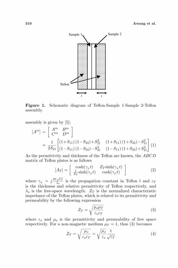
For layered samples, the S11 of the Teflon-Sample 1-Sample 2-Teflon assembly is not equal to S22 [5]. Hence, the output reflectioncoefficient, S22 was also measured. The reflection and transmissioncoefficients S11 and S21 of the double-layer sample are calculated frommeasured Sm
11 and Sm21 of the assembly by substituting the permittivity
and thickness of Teflon plates. In this case, the ABCD matrix of the
310 Awang et al.
t t
Sample 1 Sample 2
Teflon
Figure 1. Schematic diagram of Teflon-Sample 1-Sample 2-Teflonassembly.
assembly is given by [5];
[Am] =[
Am Bm
Cm Dm
]
=1
2S21
[(1+S11) (1−S22)+S2
21 (1+S11) (1+S22)−S221
(1−S11) (1−S22)−S221 (1−S11) (1+S22)+S2
21
](1)
As the permittivity and thickness of the Teflon are known, the ABCDmatrix of Teflon plates is as follows
[AT ] =[
cosh(γT t) ZT sinh(γT t)1
ZTsinh(γT t) cosh(γT t)
](2)
where γT = j2π√
εT
λois the propagation constant in Teflon t and εT
is the thickness and relative permittivity of Teflon respectively, andλo is the free-space wavelength. ZT is the normalized characteristicimpedance of the Teflon plates, which is related to its permittivity andpermeability by the following expression
ZT =√
µoµT
εoεT(3)
where εo and µo is the permittivity and permeability of free spacerespectively. For a non-magnetic medium µT = 1, thus (3) becomes
ZT =√
µo
εoεT=
õo
εo
1√εT
(4)
Progress In Electromagnetics Research B, Vol. 51, 2013 311
Substituting Zo =√
µo
εointo (4) reduces the expression to
ZT = Zo1√εT
(5)
Dividing (5) by Zo yields the normalized characteristic impedance ofTeflon
ZTN =1√εT
(6)
The ABCD matrix of the double-layer dielectric sample is denoted by[AS ], where [AS ] = [ASample1] · [ASample2], and the relationship between[Am] and [AS ] is given by the following matrix expression:
[AS ] =[AT
]−1 · [Am] · [AT]−1
(7)
The parameters S11 and S21 of Sample 2 can be obtained using thefollowing standard relations [6]:
S11 =[A + B − C −D
A + B + C + D
]S21 =
[2
A + B + C + D
](8)
After removing the effects of the Teflon plates and that of Sample 1,the system can be analyzed as a planar sample of thickness d placedin free-space. The calculated Sc
21 values can be obtained using (8)above, which, if expressed in terms of the reflection coefficient Γ andtransmission coefficient T takes the form [6]:
Sc21 = T
(1− Γ2
)
(1− Γ2T 2)(9)
Γ is the reflection coefficient of the air-Sample interface and is given as
Γ =ZSN − 1ZSN + 1
(10)
while T is the transmission coefficient given by
T = e−γd (11)
ZSN and γ are the normalized characteristic impedance andpropagation constant of the sample, and are similarly related to thepermittivity of the sample εs by (6), viz.
ZSN =1√εs
(12)
γ = γo√
εS (13)
Here γo = j2πλo
. Using Equations (5) to (9), we can therefore find Sc21
in terms of ε. However, ε cannot be expressed explicitly in terms of
312 Awang et al.
Sc21. Therefore, it is necessary to determine ε iteratively by assuming
a guess value for the sample. This is done by using a zero findingtechnique which finds the zeros of the error function, which is definedas the difference between the measured and calculated S21 values,
E = |Sm21 − Sc
21| (14)
2.2. Metal-Backed Method (MBM)
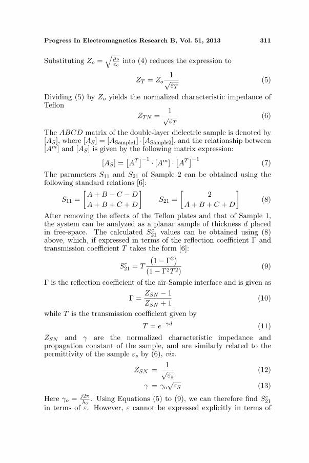
The assembly of MBM discussed by Ghodgaonkar et al. [7] has aperfectly conducting plate inserted behind an unknown one-layersample. The S11 was measured and related to the normalized waveimpedance in the unknown material. In our work, however, the sampleis a double-layered dielectric sandwiched between two Teflon quarter-wave transformers, backed by a metal plate. Fig. 2 illustrates the saidassembly.
Z 1 Z 2
Sample 1 Sample 2
MetalTeflon
Z 3Z 4
Figure 2. Schematic diagram of metal-backed method set-up.
For this method, the complex permittivity of the sample will becalculated from measured reflection coefficient Sm
11. t is the thicknessof Teflon plates, while d1 and d2 are thicknesses of Samples 1 and2 respectively. The characteristic impedances of Samples 1 and 2are similarly given by (6) previously, by substituting the permittivityof Teflon with those of the samples. The permittivity of Teflonwas determined from our own measurements, the experimental set-up of which was based on the original effort by [7]. Details of theseexperiments have been reported elsewhere [3, 8].
Progress In Electromagnetics Research B, Vol. 51, 2013 313
From transmission line theory it can be shown that the inputimpedance of the assembly is
Z1 = ZTZ2 + jZT tan βT t
ZT + jZ2 tan βT t(15)
where βT is the phase constant of Teflon given by
βT =2π√
εT
λ0(16)
The calculated Sc11 can be written as follows
Sc11 =
Z1 − 377Z1 + 377
(17)
The error function E takes the same form as (14), by replacing Sc21 with
Sc11. Further, Sc
21is obtained using (15) and (16), with the characteristicimpedances of Samples 1 and 2 calculated using (6) previously Therelative permittivity of the sample εS is again determined by findingthe zeros of the error function.
3. MEASUREMENT SETUP
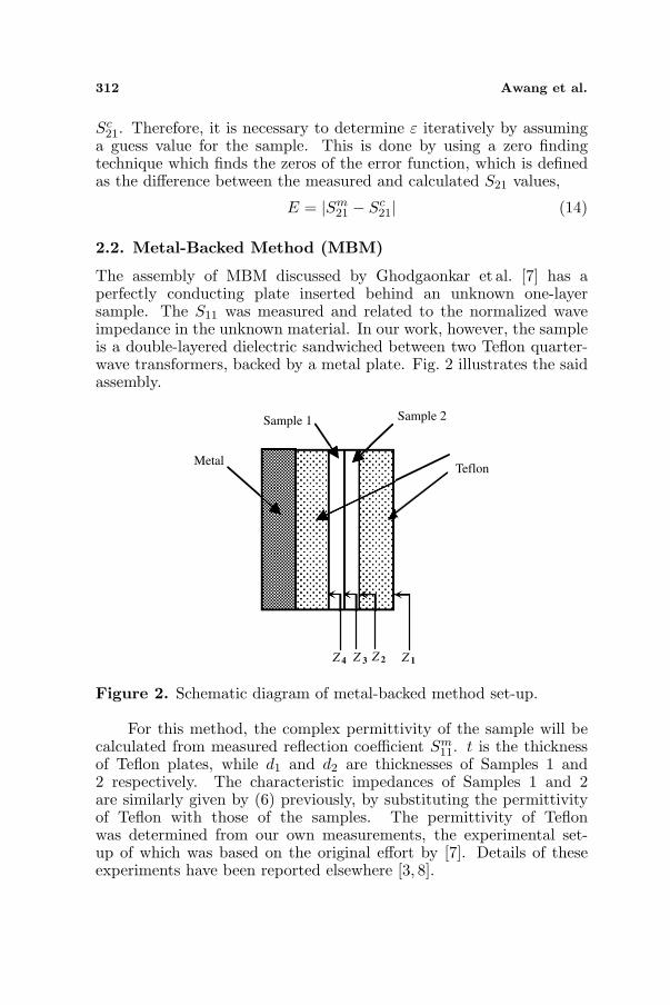
The measurement setup is shown in Fig. 3. The experiment was carriedout over a frequency range of 18–26 GHz. Two spot-focusing horn lensantennas are mounted back-to-back 610mm apart on a large table.The antennas are connected to the two ports of a Wiltron 37269BVNA using circular-to-rectangular waveguide adapters, rectangularwaveguide to coaxial line adapters, and precision coaxial cables.Millitech series WAC circular-to-rectangular waveguide adapters wereused to provide transition from standard rectangular waveguide tocircular waveguide [9]. The antennas are Gaussian optics lens antennasmanufactured by Millitech Inc. The diameter of the lens and thehousing length of the antennas were 304.8 mm each. In Gaussian optics
Spot-focusing antennaSampleSpot-focusing antenna
Figure 3. Schematic diagram of the measurement set-up.
314 Awang et al.
transmission, the propagating signal is not confined by metal or bydielectric walls, but travels in free space, resulting in a very low losssystem. The ratio of the focal distance to antenna diameter (F/D)of the lens is equal to one and D is approximately 30.5 cm. A lensantenna with its beam focused at a finite distance (typically a few lensdiameters’ length in front of the lens) can be configured for applicationsrequiring a spot beam focus [9].
A personal computer is used for FORTRAN programming. Errorsin free-space measurement of S-parameters due to multiple reflectionsbetween the antennas and the mode transitions are eliminated byimplementing LRL (Line, Reflect, Line) calibration techniques in free-space [4, 10]. Post calibration errors are minimized by using the time-domain gating feature of the VNA.
A specially fabricated sample holder is mounted at the commonfocal plane for holding planar samples. The transmit and receivehorns were mounted on a carriage and the distance between themcan be changed with an accuracy of 0.001 in. using a dial indicator.Because of spot-focusing lens antennas, diffraction effects at the edgesof the sample are negligible if the minimum transverse dimension ofthe sample is greater than three times the beamwidth of the antennaat the focus [5].
In this work, a quarter-wavelength transformer was implementedfor impedance matching. Teflon was used as a matching layer to reducethe reflectivity of the SiO2. As the measurements were done at 18to 26 GHz, the matching occurs at a mid-band frequency of 22 GHz.The thickness of Teflon matching layer is 2.35 mm. The samplesused were SiO2 grown on various doped and undoped Si substrates.The network analyzer measures the amplitude and phase of reflectedand transmitted signals in the free-space and is capable of makingaccurate measurement from 40 MHz to 40 GHz frequency range. Thepermittivity of the samples was calculated based on the measuredS11 values. For comparison, a full three-dimensional electromagneticsimulation was carried out using an industry-standard electromagneticsimulator CST Microwave Studio.
4. EXPERIMENTAL RESULTS AND DISCUSSIONS
4.1. Double-Layer Bulk Dielectrics
In this work, the double-layer bulk dielectric samples were arrangedas Sample 1-Sample 2. Two sets of samples were used, one eachfor transmission and metal-backed methods. For the transmissionmethod, the samples used were Plexiglas-PVC and PVC-Plexiglas,while Plexiglas-PVC and Teflon-PVC were used in the metal-back
Progress In Electromagnetics Research B, Vol. 51, 2013 315
procedure. The thicknesses of the samples are 5.8 mm (Plexiglas)and 3.0 mm (Teflon and PVC). In order to reduce the measurementerrors, the sample thickness was required to be close to odd multiplesof quarter wavelength [7]. This therefore limits the frequency rangeover which the samples can be measured.
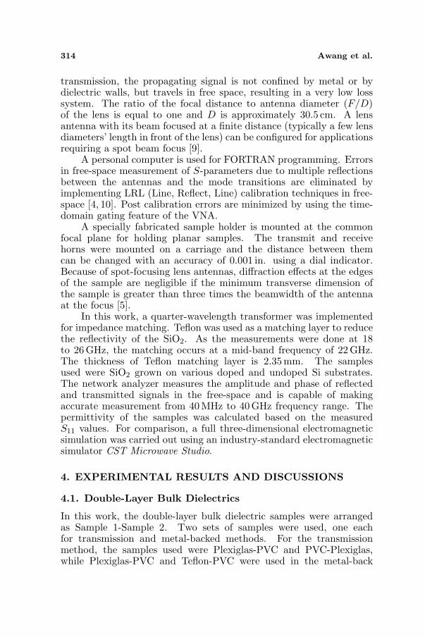
In the transmission method arrangement, and in accordance withEquations (7) to (9), the unknown dielectric is denoted as Sample 2.For the PVC-Plexiglas combination for example, the unknown is thePlexiglas, and thus the measured values were those of Plexiglas. Themeasured ε′ values are plotted in Fig. 4 above for Plexiglas (greentrace) and PVC (red) respectively. Using the transmission method, therelative permittivity for PVC was found to be between 2.65 to 2.93,and for Plexiglas between 2.45 to 2.63. The mean values for PVC andPlexiglas were 2.81 and 2.55 respectively — these compare favourablywith those reported in the literature (2.81 against 2.9 for PVC [7], and2.55 against 2.59 for Plexiglas [10]). From the graph it can be seenthat both sets exhibit an almost similar trend for frequencies lowerthan about 24 GHz, but the trend differ slightly beyond that, with thePlexiglas showing an upward trend in contrast to PVC. The decreasein ε′ for PVC could be attributed to the quality of the samples used,which could have been caused by manufacturing. The fluctuation of thevalues above 22GHz may have been caused by errors of the measuredS11, S21, and S22 and air gap that could have existed in the sampleassembly. Nevertheless, these fluctuations are of the order of 3 to4% only, and can therefore be considered small. The fact that thesefluctuations are small, and that the measured values compare very wellwith those reported in the literature imply that this method is capableof yielding acceptable accuracies in real applications.
Plexiglas-PVC
PVC-Plexiglas
Rel
ativ
e P
erm
ititiv
ity (ε
')
3.00
2.80
2.60
2.40
2.2020.0 21.0 22.0 23.0
2.90
2.70
2.50
2.30
18.0 19.0 24.0 25.0 26.0Frequency (GHz)
Figure 4. Measured relative permittivity values using thetransmission method.
316 Awang et al.
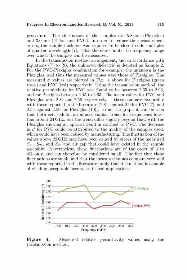
Figure 5 shows the plot of measured ε′ obtained from the metal-backed method. With the metal-backed method, the measured valuesof ε′ for Plexiglas-PVC were between 2.26 to 3.09, and between 2.60 to2.93 for Teflon-PVC. The mean values are 2.98 and 2.73 respectively,which agree well with the published value of 2.9 [7].
Plexiglas-PVC
Teflon-PVC
3.60
3.40
3.20
3.00
2.80
2.60
2.40
2.20
2.0020.020.0 21.0 22.0 23.0
Frequency (GHz)
ε'
Figure 5. Measured relative permittivity values using the metal-backed method.
4.2. Thin Film Dielectric
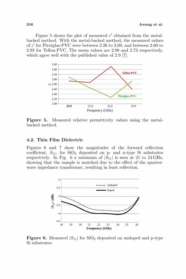
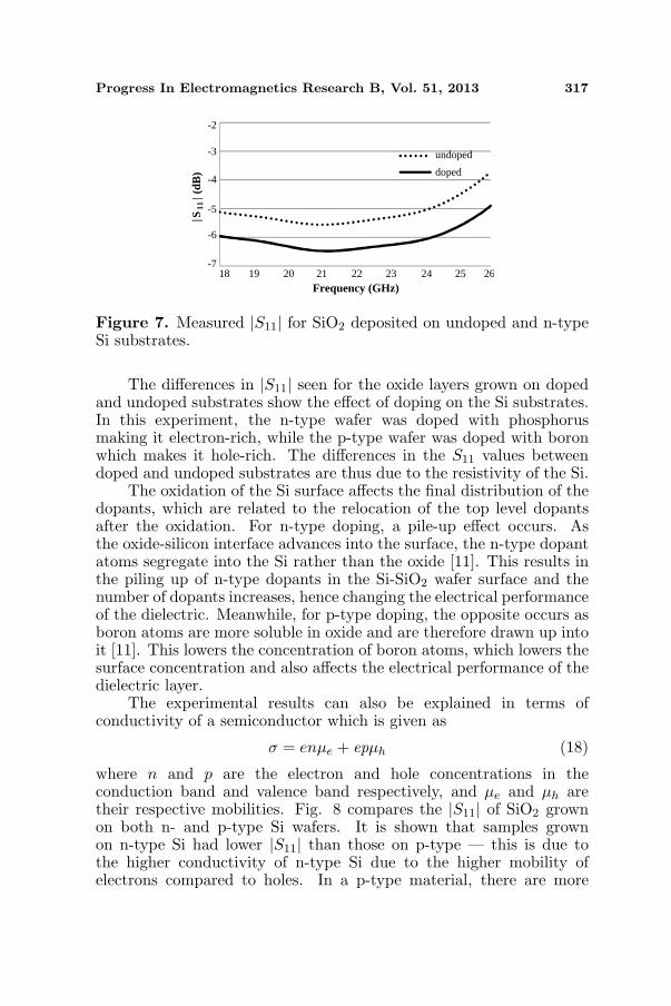
Figures 6 and 7 show the magnitudes of the forward reflectioncoefficient, S11, for SiO2 deposited on p- and n-type Si substratesrespectively. In Fig. 6 a minimum of |S11| is seen at 21 to 24 GHz,showing that the sample is matched due to the effect of the quarter-wave impedance transformer, resulting in least reflection.
| S
(d
B)
|
-2
-2.5
-3
-4
-4.5
-3.5
undoped
doped
18 19 20 21 22 23 24 25 26Frequency (GHz)
11
Figure 6. Measured |S11| for SiO2 deposited on undoped and p-typeSi substrates.
Progress In Electromagnetics Research B, Vol. 51, 2013 317
| S
(d
B)
|
-2
-3
-4
-5
18 19 20 21 22 23 24 25 26Frequency (GHz)
11
undoped
doped
-6
-7
Figure 7. Measured |S11| for SiO2 deposited on undoped and n-typeSi substrates.
The differences in |S11| seen for the oxide layers grown on dopedand undoped substrates show the effect of doping on the Si substrates.In this experiment, the n-type wafer was doped with phosphorusmaking it electron-rich, while the p-type wafer was doped with boronwhich makes it hole-rich. The differences in the S11 values betweendoped and undoped substrates are thus due to the resistivity of the Si.
The oxidation of the Si surface affects the final distribution of thedopants, which are related to the relocation of the top level dopantsafter the oxidation. For n-type doping, a pile-up effect occurs. Asthe oxide-silicon interface advances into the surface, the n-type dopantatoms segregate into the Si rather than the oxide [11]. This results inthe piling up of n-type dopants in the Si-SiO2 wafer surface and thenumber of dopants increases, hence changing the electrical performanceof the dielectric. Meanwhile, for p-type doping, the opposite occurs asboron atoms are more soluble in oxide and are therefore drawn up intoit [11]. This lowers the concentration of boron atoms, which lowers thesurface concentration and also affects the electrical performance of thedielectric layer.
The experimental results can also be explained in terms ofconductivity of a semiconductor which is given as
σ = enµe + epµh (18)
where n and p are the electron and hole concentrations in theconduction band and valence band respectively, and µe and µh aretheir respective mobilities. Fig. 8 compares the |S11| of SiO2 grownon both n- and p-type Si wafers. It is shown that samples grownon n-type Si had lower |S11| than those on p-type — this is due tothe higher conductivity of n-type Si due to the higher mobility ofelectrons compared to holes. In a p-type material, there are more
318 Awang et al.
p-type
| S
(d
B)
|
-2
-3
-4
-5
18 19 20 21 22 23 24 25 26Frequency (GHz)
11
-6
0
-1n-type
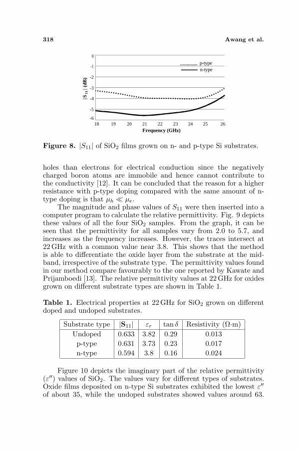
Figure 8. |S11| of SiO2 films grown on n- and p-type Si substrates.
holes than electrons for electrical conduction since the negativelycharged boron atoms are immobile and hence cannot contribute tothe conductivity [12]. It can be concluded that the reason for a higherresistance with p-type doping compared with the same amount of n-type doping is that µh ¿ µe.
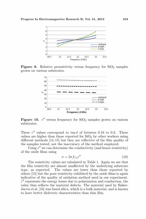
The magnitude and phase values of S11 were then inserted into acomputer program to calculate the relative permittivity. Fig. 9 depictsthese values of all the four SiO2 samples. From the graph, it can beseen that the permittivity for all samples vary from 2.0 to 5.7, andincreases as the frequency increases. However, the traces intersect at22GHz with a common value near 3.8. This shows that the methodis able to differentiate the oxide layer from the substrate at the mid-band, irrespective of the substrate type. The permittivity values foundin our method compare favourably to the one reported by Kawate andPrijamboedi [13]. The relative permittivity values at 22 GHz for oxidesgrown on different substrate types are shown in Table 1.
Table 1. Electrical properties at 22 GHz for SiO2 grown on differentdoped and undoped substrates.
Substrate type |S11| εr tan δ Resistivity (Ω·m)Undoped 0.633 3.82 0.29 0.013p-type 0.631 3.73 0.23 0.017n-type 0.594 3.8 0.16 0.024
Figure 10 depicts the imaginary part of the relative permittivity(ε′′) values of SiO2. The values vary for different types of substrates.Oxide films deposited on n-type Si substrates exhibited the lowest ε′′of about 35, while the undoped substrates showed values around 63.
Progress In Electromagnetics Research B, Vol. 51, 2013 319
undopedp-type
20.5 21 21.5 23Frequency (GHz)
ε'
7
6
5
4
3
2
1
022 22.5 23.5
n-type
Figure 9. Relative permittivity versus frequency for SiO2 samplesgrown on various substrates.
Frequency (GHz)20.5 21 21.5 22 22.5 23 23.5
70
60
50
40
30
20
10
0
ε''
undopedp-typen-type
Figure 10. ε′′ versus frequency for SiO2 samples grown on varioussubstrates.
These ε′′ values correspond to tan δ of between 0.16 to 0.3. Thesevalues are higher than those reported for SiO2 by other workers usingdifferent methods [14, 15] but they are reflective of the film quality ofthe samples tested, not the inaccuracy of the method employed.
Using ε′′ we can determine the conductivity (and hence resistivity)of the oxide films using
σ = 2πfεoε′′ (19)
The resistivity values are tabulated in Table 1. Again we see thatthe film resistivity are almost unaffected by the underlying substratetype, as expected. The values are lower than those reported byothers [15] but the poor resistivity exhibited by the oxide films is againindicative of the quality of oxidation method used in our experiment.ε′′ represents the energy losses due to polarization and conduction, thevalue thus reflects the material defects. The material used by Baker-Jarvis et al. [16] was fused silica, which is a bulk material, and is knownto have better dielectric characteristics than thin film.
320 Awang et al.
4.2.1. Comparison with Simulation
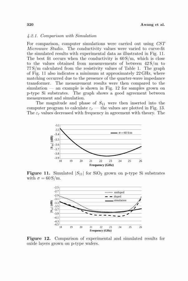
For comparison, computer simulations were carried out using CSTMicrowave Studio. The conductivity values were varied to curve-fitthe simulated results with experimental data as illustrated in Fig. 11.The best fit occurs when the conductivity is 60 S/m, which is closeto the values obtained from measurements of between 42 S/m to77 S/m calculated from the resistivity values of Table 1. The graphof Fig. 11 also indicates a minimum at approximately 22 GHz, wherematching occurred due to the presence of the quarter-wave impedancetransformer. The measurement results were then compared to thesimulation — an example is shown in Fig. 12 for samples grown onp-type Si substrates. The graph shows a good agreement betweenmeasurement and simulation.
The magnitude and phase of S11 were then inserted into thecomputer program to calculate εr — the values are plotted in Fig. 13.The εr values decreased with frequency in agreement with theory. The
| S
(d
B)
|
-3.4
-3.5
-3.6
-3.7
18 19 20 21 22 23 24 25 26Frequency (GHz)
11
-3.8
-3.2
-3.3
-3.9
σ = 60 S/m
Figure 11. Simulated |S11| for SiO2 grown on p-type Si substrateswith σ = 60 S/m.
| S
(d
B)
|
18 19 20 21 22 23 24 25 26Frequency (GHz)
11
undoped
dopedsimulation
-2.5-2.7
-2.9-3.1-3.3-3.5-3.7-3.9-4.1-4.3-4.5
Figure 12. Comparison of experimental and simulated results foroxide layers grown on p-type wafers.
Progress In Electromagnetics Research B, Vol. 51, 2013 321
Frequency (GHz)
Rel
ativ
e pe
rmitt
ivity
6
5.5
5
4.5
4
3.5
3
2.5
218 19 20 21 22 23 24 25 26
Figure 13. Simulated εr values against frequency.
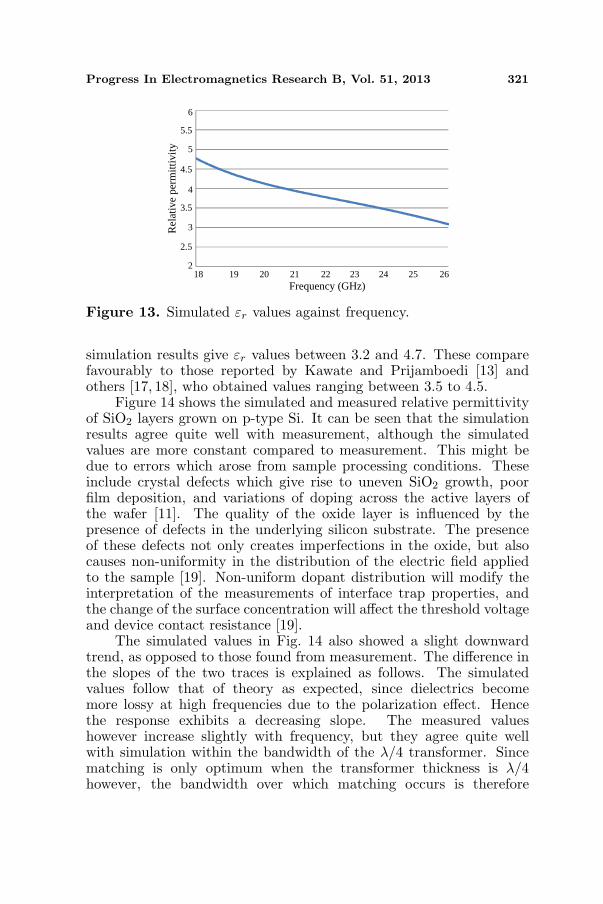
simulation results give εr values between 3.2 and 4.7. These comparefavourably to those reported by Kawate and Prijamboedi [13] andothers [17, 18], who obtained values ranging between 3.5 to 4.5.
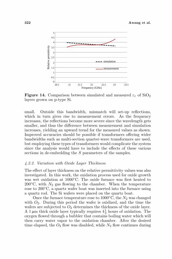
Figure 14 shows the simulated and measured relative permittivityof SiO2 layers grown on p-type Si. It can be seen that the simulationresults agree quite well with measurement, although the simulatedvalues are more constant compared to measurement. This might bedue to errors which arose from sample processing conditions. Theseinclude crystal defects which give rise to uneven SiO2 growth, poorfilm deposition, and variations of doping across the active layers ofthe wafer [11]. The quality of the oxide layer is influenced by thepresence of defects in the underlying silicon substrate. The presenceof these defects not only creates imperfections in the oxide, but alsocauses non-uniformity in the distribution of the electric field appliedto the sample [19]. Non-uniform dopant distribution will modify theinterpretation of the measurements of interface trap properties, andthe change of the surface concentration will affect the threshold voltageand device contact resistance [19].
The simulated values in Fig. 14 also showed a slight downwardtrend, as opposed to those found from measurement. The difference inthe slopes of the two traces is explained as follows. The simulatedvalues follow that of theory as expected, since dielectrics becomemore lossy at high frequencies due to the polarization effect. Hencethe response exhibits a decreasing slope. The measured valueshowever increase slightly with frequency, but they agree quite wellwith simulation within the bandwidth of the λ/4 transformer. Sincematching is only optimum when the transformer thickness is λ/4however, the bandwidth over which matching occurs is therefore
322 Awang et al.
Frequency (GHz)
Rel
ativ
e pe
rmitt
ivity
5
4.5
4
3.5
3
2.5
2
1.5
1
0.5
020.5 21 21.5 22 22.5 23 23.5
simulation
measurement
Figure 14. Comparison between simulated and measured εr of SiO2
layers grown on p-type Si.
small. Outside this bandwidth, mismatch will set-up reflections,which in turn gives rise to measurement errors. As the frequencyincreases, the reflections become more severe since the wavelength getssmaller, and thus the difference between measurement and simulationincreases, yielding an upward trend for the measured values as shown.Improved accuracies should be possible if transformers offering widerbandwidths such as multi-section quarter-wave transformers are used,but employing these types of transformers would complicate the systemsince the analysis would have to include the effects of these varioussections in de-embedding the S parameters of the samples.
4.2.2. Variation with Oxide Layer Thickness
The effect of layer thickness on the relative permittivity values was alsoinvestigated. In this work, the oxidation process used for oxide growthwas wet oxidation at 1000C. The oxide furnace was first heated to200C, with N2 gas flowing to the chamber. When the temperaturerose to 200C, a quartz wafer boat was inserted into the furnace usinga quartz rod. The Si wafers were placed on the quartz boat.
Once the furnace temperature rose to 1000C, the N2 was changedwith O2. During this period the wafer is oxidized, and the time thewafers are subjected to O2 determines the thickness of the oxide layer.A 1 µm thick oxide layer typically requires 41
2 hours of oxidation. Theoxygen flowed through a bubbler that contains boiling water which willthen carry water vapor to the oxidation chamber. After the desiredtime elapsed, the O2 flow was disabled, while N2 flow continues during
Progress In Electromagnetics Research B, Vol. 51, 2013 323
ramp down. At approximately 500C, the N2 flow was disabled andthe wafers were left overnight for cooling down to room temperaturebefore being taken out.
In this work, the oxide film thickness was determined usingFilmetrics F20, a general purpose film thickness measurementinstrument. The instrument uses a technique called spectralreflectance, where the film thickness is measured by reflecting light offthe film and analyzing the reflected light over a range of wavelengths.The instrument can measure film thicknesses from 3 nm up to 1mm.
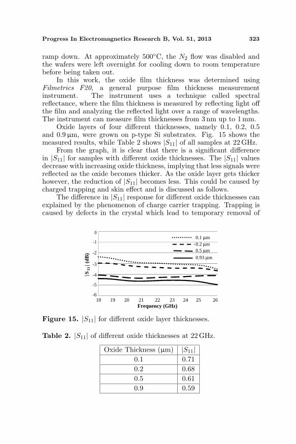
Oxide layers of four different thicknesses, namely 0.1, 0.2, 0.5and 0.9µm, were grown on p-type Si substrates. Fig. 15 shows themeasured results, while Table 2 shows |S11| of all samples at 22 GHz.
From the graph, it is clear that there is a significant differencein |S11| for samples with different oxide thicknesses. The |S11| valuesdecrease with increasing oxide thickness, implying that less signals werereflected as the oxide becomes thicker. As the oxide layer gets thickerhowever, the reduction of |S11| becomes less. This could be caused bycharged trapping and skin effect and is discussed as follows.
The difference in |S11| response for different oxide thicknesses canexplained by the phenomenon of charge carrier trapping. Trapping iscaused by defects in the crystal which lead to temporary removal of
0.1 µm0.2 µm0.5 µm
0.93 µm
| S
(d
B)
|
-2
-3
-4
-5
18 19 20 21 22 23 24 25 26Frequency (GHz)
11
-6
0
-1
Figure 15. |S11| for different oxide layer thicknesses.
Table 2. |S11| of different oxide thicknesses at 22 GHz.
Oxide Thickness (µm) |S11|0.1 0.710.2 0.680.5 0.610.9 0.59
324 Awang et al.
the electron from the conduction band [12]. There are four generaltypes of charges associated with the SiO2-Si system, namely fixedoxide charge, mobile oxide charge, trapped oxide charge, and trappedinterface charge.
The interface trapped charges are positive or negative charges,created due to structural defects, oxidation-induced defects, metalimpurities, or other defects caused by radiation or similar bond-breaking processes [20]. These trapped charges are located at the Si-SiO2 interface, whereby their concentration increased with the oxidethickness [21]. This could be explained by the fact that more holeswere attracted towards the Si/SiO2 interface as the oxide thicknessdecreases. The inversion holes weaken the Si-H bonds, leading to thecreation of more trapped charges [22, 23].
When RF signals are applied to the sample, the high operatingfrequency resulted in the period of the applied signal to becomecomparable to the time constant of the trapping and de-trapping ofthe interface states. Kwan and Deen [24] found in their measurementsthat carrier trapping affected S-parameter measurements, whereby the|S11| increased with increasing interface traps. They also reported thatelectron mobility decreases with increasing interface traps. Based onthese arguments, it can be proposed that interface traps exist more inthinner oxides where it reduces the electron mobility, hence decreasingthe conductivity. This supports the notion that |S11| increases withdecreasing oxide thickness as the result of charge trapping.
The effect of oxide layer thickness on S11 response may bediscussed further based on surface potential, which is generated bya difference in the work function of the materials used. Nevin andChamberlain [25] studied the effect of oxide thickness on the propertiesof metal-insulator-semiconductor device and found that the surfacepotential of the device is lowered with thicker oxide layers. As thelayer gets thicker, the surface potential decreases, reducing the fieldstrength in the process.
The change in |S11| is directly related to changes in the surfacepotential which result from the field associated with the charges of thelayer. The reflection coefficient |S11| is proportional to the ratio of theincident electric field Eo to the reflected field Er;
|S11| ∝ Er
Eo(20)
When the oxide layer gets thicker, the surface potential reduces andthis lowers the electric field associated with it. From (20) we see that,for the same electric field incident on the samples, as the oxide thicknessis increased, the reflected field is thus reduced, and this leads to areduction in |S11|.
Progress In Electromagnetics Research B, Vol. 51, 2013 325
The effect of oxide thickness can be further discussed by the losstangent, tan δ, which is a measure of the energy loss due to microwaveabsorption within the material. The loss tangent is the ratio of ε′′ toε′, and is also related to the oxide thickness as follows [26]:
tan δ =ε′′
ε′=
12
(ed
2
)1/2 (nεo
2πε∞kT
)1/4
(21)
where d is the oxide thickness, k is the Boltzmann’s constant, ε∞ theradio frequency relative permittivity, and T the temperature. Thecarrier density n is independent of thickness, while tan δ varies withd1/2. It can be shown further that tan δ depends on the conductivitythrough the relation [26]
ε′′ =σ
ω(22)
From (21) we see that as the oxide layer gets thinner, tan δ decreases,and from (22), the conductivity decreases in the process, leading to anincrease in |S11| as seen in the experiment.
Ismail et al. [27] studied the reflection characteristics of dielectricsubstrates having a variety of relative permittivity and loss tangentvalues, and reported that samples with higher ε and loss tangentabsorb more incident signal. This was explained by the fact that theincreasing ε and loss tangent causes more multiple reflections in thedielectric, thus dissipating more energy in the dielectric [27]. This leadsto degradation in the reflectivity of the dielectric, which concurs withthe behavior we see with our samples in this experiment.
4.2.3. Skin Effect
At microwave frequencies, the penetration of currents and magneticfields into the surface of a material is governed by skin effect. Skineffect is the tendency for high frequency alternating currents andmagnetic flux to penetrate into the surface of a conductor only to alimited depth [28]. Skin effect, δ, also termed as ‘depth of penetration’,depends on the frequency, f , the conductivity, σ, and the permeabilityof the material, µ. If the thickness of a material is much greaterthan the depth of penetration, its behavior toward high frequencyalternating currents becomes a surface phenomenon rather than avolume phenomenon [28].
In this experiment, the conductivity of the SiO2 was deducedfrom the electromagnetic simulation through optimization. For aconductivity value of 60 S/m, the calculated skin effect is 0.5µm. Itcan be seen from Table 1 that as the oxide thickness becomes greaterthan 0.5µm, the S11 reduction becomes less compared to the reduction
326 Awang et al.
seen in the range 0.1 to 0.5µm. This seems to imply that as the oxidelayer gets thicker than the skin depth, more RF signals are confinedin the skin depth, and thus the reflection which resulted is more dueto the surface, rather than bulk, phenomenon. This result also showsthat the measurement technique is reliable because it is sensitive to theproperties of the epitaxial layer only. The presence of the substrate,whose conductivity is several orders of magnitude larger than the layerto be measured, did not seem to affect the data measured [29].
5. CONCLUSIONS
A non-destructive, non-contact technique for measuring the complexpermittivity of double-layer bulk dielectric and thin film dielectricat microwave frequencies has been developed. The set up consistedof spot-focusing horn antennas and a vector network analyzer formeasuring the reflected signals. Two methods were used in theexperiments — Metal-Backed Method for thin film dielectric, andTransmission Method and Metal-Backed Method for bulk dielectrics.The quarter-wave transformers used improved the matching at themiddle of the frequency band.
The permittivity values found for both bulk and thin filmdielectrics compared favourably to those reported in literature. Thevalues found for PVC and Plexiglas differ from published data byless than 1%, while those of SiO2 agreed to within 2% of thereported figures. More importantly, the method allows accuratecharacterization of the epitaxial layers of a semiconductor wafer bybeing able to isolate the effect of the underlying substrate providedthe film thicknesses were less than the skin depth. These results showthe important contribution of this work in characterizing thin filmsat microwave frequencies. The fact that the method is both non-contacting and non-destructive leads to the reduction of errors due tocontact resistance and parasitics, both of which are normally significantat high frequencies.
ACKNOWLEDGMENT
The authors would like to acknowledge Universiti Teknologi MARAfor funding this work under the Dana Kecemerlangan research fund.
REFERENCES
1. Hambley, A. R., Electronics, 2nd edition, Prentice-Hall Interna-tional, Inc., New Jersey, 2000.
Progress In Electromagnetics Research B, Vol. 51, 2013 327
2. Ahmad, S., Microwave and Millimeter Wave SemiconductorMaterials Technology, Tata McGraw-Hill, New York, 1998.
3. Baba, N. H., Z. Awang, and D. K. Ghodgaonkar, “Accuracyconsiderations for dielectric measurements of semiconductorwafers using free space microwave measurement system in 8–13GHz range,” Proc. IEEE Int. RF and Microwave Conf. (RFM),177–181, Kuala Lumpur, Oct. 5–6, 2004.
4. Saad, T. S., R. C. Hansen, and G. J. Wheeler, MicrowaveEngineers’ Handbook, Vol. 1., 179, Artech House, Boston, 1971.
5. Ghodgaonkar, D. K., V. V. Varadan, and V. K. Varadan,“Free-space measurement of complex permittivity and complexpermeability of magnetic materials at microwave frequencies,”IEEE Trans. of Inst. and Measurement, Vol. 39, No. 2, 387–394,Apr. 1990.
6. Srivastava, G. P. and V. L. Gupta, Microwave Devices and CircuitDesign, Prentice-Hall India, New Delhi, 2006.
7. Ghodgaonkar, D. K., V. V. Varadan, and V. K. Varadan, “Afree-space method for measurement of dielectric constants andloss tangents at microwave frequencies,” IEEE Trans. of Inst. andMeasurement, Vol. 38, No. 3, 789–793, Jun. 1989.
8. Baba, N. H., Microwave Non-destructive Testing of SemiconductorMaterials, M.Sc. thesis, Universiti Teknologi MARA, Apr. 2005.
9. Millitech, Inc., Series GOA Gaussian Optics Lens Antenna.10. Hippel, A. V., Dielectric Materials and Applications, Artech
House, Boston, 1995.11. Zant, P. V., Microchip Fabrication, 5th Edition, McGraw-Hill,
New York, 2004.12. Kasap, S. O., Principles of Electronic Materials and Devices, 2nd
Edition, McGraw-Hill, New York, 2002.13. Kawate, E. and B. Prijamboedi, “Development of the measure-
ment method of dielectric constant of low-k film in the millimeterwave region,” Proc. Joint 29th Int. Conf. on Infrared and Millime-ter Waves and 12th Int. Conf. on Terahertz Electronics, 801–802,Karlsruhe, Germany, Oct. 2004.
14. Bakker, G. L. and D. W. Hess, “Removal of thermally grownSiO2 films using water at elevated temperature and pressure,”Electrochem. Soc. Proc., Vol. 95–20, 464–471, 1996.
15. Harper, C. A., Handbook of Ceramics, Glasses and Diamonds,McGraw-Hill, New York, 2001.
16. Baker-Jarvis, J., et al., “Dielectric characterization of low-lossmaterials: A comparison technique,” IEEE Trans. Dielectric Elect.
328 Awang et al.
Ins., Vol. 5, No. 4, 571–577, Aug. 1998.17. Albertin, K. F., M. A. Valle, and I. Pereyra, “Study of MOS
capacitors with TiO2 and SiO2/TiO2 gate dielectric,” J. Int. Cir.Systems, Vol. 2, 89–93, 2007.
18. Shackelford, J. F., W. Alexander, and J. S. Park, MaterialsScience and Engineering, 2nd Edition, CRC Press, Inc., BocaRaton, 1994.
19. May, G. S. and S. M. Sze, Fundamentals of SemiconductorFabrication, John Wiley and Sons, New York, 2004.
20. Schroder, D. K., Semiconductor Material and Device Characteri-zation, 2nd Edition, John Wiley & Sons, Inc., New York, 2004.
21. Hadi, D. A., S. F. W. M. Hatta, and N. Soin, “Effect of oxidethickness on 32 nm PMOSFET reliability,” Proc. IEEE Int. Conf.on Semicond. Electron. (ICSE), 244–247, Jun. 28–30, 2010.
22. Mahapatra, S., M. A. Alam, P. B. Kumar, T. R. Dalei,D. Varghese, and D. Saha, “Negative bias temperature instabilityin CMOS devices,” Microelectronics Eng., Vol. 80, 114–121, 2005.
23. Alam, M. A., H. Kufluoglu, D. Varghese, and S. Mahapatra,“A comprehensive model for PMOS NBTI degradation: Recentprogress,” Microelectronics Rel., Vol. 47, 853–862, Dec. 2006.
24. Kwan, W. S. and M. J. Deen, “Hot-carrier effects on thescattering parameters of lightly doped drain n-type metal-oxide-semiconductor field effect transistor,” J. Vac. Sci. Technol.,Vol. 16, No. 2, 628–632, Jan. 1998.
25. Nevin, W. A. and G. A. Chamberlain, “Effect of oxide thicknesson the properties of metal-insulator-organic semiconductorphotovoltaic cells,” IEEE Trans. on Electron. Devices, Vol. 40,No. 1, 75–81, Jan. 1993.
26. Burkhardt, P. J., “Dielectric relaxation in thermally grown SiO2
films,” IEEE Trans. on Elect. Dev., Vol. 13, No. 2, 268–275,Feb. 1966.
27. Ismail, M. Y., M. Inam, and A. M. A. Zaidi, “Reflectivity ofreflectarrays based on dielectric substrates,” Amer. J. of Eng.Appl. Sci., Vol. 3, No. 1, 180–185, 2010.
28. Wheeler, H. A., “Formulas for the skin effect,” Proc. of the IRE,Vol. 30, No. 9, 412–424, Sept. 1942.
29. Bichara, M. R. E. and J. P. R. Poitevin, “Resistivity measurementof semiconducting epitaxial layers by the reflection of ahyperfrequency electromagnetic wave,” IEEE Trans. Inst. Meas.,Vol. 13, 323–328, Dec. 1964.


![A COMPARISON OF GENETIC ALGORITHMS, PARTI ... › PIERB › pierb13 › 09.09011308.pdfalgorithms include Genetic Algorithms (GA) [1{5], Particle Swarm Optimization (PSO) [11{13],](https://img.pdfslide.us/doc/110x75/5f0d0b167e708231d4386595/a-comparison-of-genetic-algorithms-parti-a-pierb-a-pierb13-a-09-algorithms.jpg)