Embed Size (px)
Citation preview

Int J Fract (2019) 216:161–171https://doi.org/10.1007/s10704-019-00350-4
ORIGINAL PAPER
A fracture model for exfoliation of thin silicon films
Martin Ward · Michael Cullinan
Received: 26 September 2018 / Accepted: 6 February 2019 / Published online: 14 February 2019© Springer Nature B.V. 2019
Abstract The direct exfoliation of thin films from sil-icon wafers has the potential to significantly lower thecost of flexible electronics while leveraging the per-formance benefits and established infrastructure of tra-ditional wafer-based fabrication processes. However,controlling the thickness and uniformity of exfoliatedsilicon thin films has proven difficult due to a lackof understanding and control over the exfoliation pro-cess. This paper presents a new silicon exfoliationprocess and model which enables accurate predictionof the thickness and quality of the exfoliated thin-film based on the exfoliation process parameters. Thismodel uses a parametric, finite element, linear elas-tic fracture mechanics study with nonlinear loadingto determine how each process parameter affects thecrack propagation depth. A metamodel is then con-structed from the results of numerous simulations toinform the design and operation of a novel exfolia-tion tool and predict thickness of produced films. Inorder to manufacture uniform, high-quality films, thetool creates a controlled peeling load that is able topropagate a crack through the silicon in a controlledmanner. Finally, exfoliated silicon samples producedwith the prototype tool are evaluated and compared tometamodel projections, confirming the ability of thetool to steer crack trajectory within ± 3 microns of thecrack depth predictions.
M. Ward · M. Cullinan (B)Department of Mechanical Engineering, University ofTexas at Austin, Austin, TX 78712, USAe-mail: [email protected]
Keywords Exfoliation · Single crystal silicon · Finiteelement analysis · Spalling
1 Introduction
In recent years, flexible electronic devices have gainedincreased traction in the market and have becomesignificantly more sophisticated (Pang et al. 2013).Notable areas of development include wearable elec-tronics (Kim et al. 2014; Ying et al. 2012), and pho-tovoltaics (Pudasaini et al. 2014; Ahn et al. 2017;Pagliaro et al. 2008). To achieve flexibility, these sys-tems generally employ new materials and fabricationtechniques that are inherently flexible, such as thin-filmsolar cells or organic or oxide-based (Fortunato et al.2012) thin-film-transistors built on polymer substrates(Pagliaro et al. 2008). These solutions either result inlower performance or place the rigid traditional com-plementary metal–oxide–semiconductor (CMOS) fab-ricated integrated circuits on a separate rigid moduleor in a discretized array (Takei et al. 2010). The use ofthin-film monocrystalline silicon (c-Si) could improvethe performance of these flexible electronic devices byallowing high-quality CMOS devices to be fabricateddirectly on flexible substrates, thus creating opportu-nities for development of entirely new applications offlexible electronics.
Exfoliation is a promising method for creatingcost-effective thin-film c-Si while leveraging existingCMOS infrastructure. This method of thin-film layer
123

162 M. Ward, M. Cullinan
Fig. 1 Controlled peelingprocess diagram
SiliconNickel
Tension
Rollers
Handle Film
SiliconNickel
3. Exfoliate Silicon1. Electroplate Nickel
2. Induce Stress
transfer often referred to as “spalling”, “large-area lift-off”, and “kerfless wafering”, all describing a processinwhich a stress field created by a tensile filmdepositedon top of a bulk substrate propagates a brittle frac-ture just beneath the surface of the substrate. This phe-nomenon often appears in other fields as a mode offailure. For example, the coating of dissimilar materi-als coupled with thermal- or deposition-related stressescan cause the structure to fracture and fail inmany semi-conductor manufacturing processes. The first mentionof exfoliation as a method of manufacturing thin c-Sifilms was made in a patent by Tanielian et al. (1986),though results were never discussed in literature. Thefirst demonstration of exfoliation of thin-film silicon inliterature was performed by Dross et al. (2007) usingprinted metal pastes as the tensile layer which werethen dried and annealed. Exfoliation occurred sponta-neously due to an excess of stress created by the mis-match in coefficients of thermal expansion (CTE) as theassembly cooled from the annealing temperature.Othermethods of exfoliation developed by R. Rao and L.Mathew from University of Texas at Austin (Rao et al.2011; Mathew and Jawarani 2010; Zhai et al. 2012)and D. Shahjerdi and S. Bedell from IBM (Bedell et al.2012, 2013a, b; Shahrjerdi andBedell 2013; Shahrjerdiet al. 2012) provide more control over the stress in thetensile film, and therefore the resulting silicon film.Both methods deposit a layer of nickel on top of the sil-icon wafer with a residual stress that is just below whatis required to spontaneously initiate a crack. Then, anadditional load is applied to propagate the crack. RaoandMathewused awedge tool to apply load to the cracktip while Shahjerdi and Bedell used adhesive tape as apeeling handle. The method of exfoliation presentedhere combines features from those described above butadds a critical element of control to the external appliedloading.
The work presented in this paper is a model formu-lation to better understand the exfoliation process and
accurately control the parameters that affect the thick-ness and quality of the resulting films. The exfoliationphenomenon in silicon is an example of brittle frac-ture. Due to the silicon wafer’s single crystal structureand very brittle nature, it can be modeled using linearelastic fracture mechanics. The goal of the model isto be able to predict the crack propagation depth fora given loading. To do this, we focus on the Mode I(KI ) and Mode II (KI I ) stress intensity factors (SIFs).The SIFs are a means of estimating the stress fields atthe crack tip where KI describes an opening mode ofthe crack and KI I describes a shearing mode. Previouswork by Thouless et al. (1987) in studying interfacialfracture phenomenon indicates that, for a given elas-tic system, a crack has a stable propagation depth thatis controlled by a tendency of KI I towards zero. Themodel presented here provides insight as to how a toolcould be designed to use this phenomenon to steer thecrack to a desired depth and, thereby, create siliconfilms of a desired thickness. A diagram of the proposedmechanism is shown in Fig. 1, where control of handletension and roller height can be used to modulate thestress fields around the crack tip.
A layer of nickel is electrodeposited on a c-Si waferand a tensile stress designed to be just below the thresh-old for spontaneously initiating a crack is induced ther-mally. The wafer is then fixed to a rigid substrate andthe film is exfoliated. The controlled peeling conceptuses two idler rollers to control the angle and tension inthe handle film, which is fixed to ground at one end andto the nickel tensile layer at the other. The rollers arethen moved across the wafer by a linear actuator. Thisprovides control of the rate at which energy is addedto the crack. The tension in the film and the height andorientation of the rollers can be adjusted to alter theloads applied to the tensile layer and then to the cracktip. This load is used to steer the crack. A series ofexperiments were performed to test the capabilities ofthe tool and performance of the model.
123

A fracture model for exfoliation of thin silicon films 163
In this paper, we first review the analytical back-ground of the thin-film fracture problem in Sect. 2.We will then define and construct a parametric FEAmodel of the exfoliation process in Sect. 3. The resultsof the FEA model and their integration into a meta-model will then be presented in Sect. 4. Finally, exper-imental results from the new exfoliation tool will bepresented in Sect. 5 and compared to the metamodelpredictions.
2 Fracture system and analytical background
Efforts to understand the exfoliation phenomenonbegan mainly as a means of avoiding the failure ofcoated films in a variety of applications including elec-tronic device manufacturing (Cannon et al. 1985; Suoand Hutchinson 1989; Xu et al. 1993). It was observedin literature that under certain conditions, interfacialfractures follow a trajectory down into the substrateand then level out at a depth characteristic of the sys-tem and the loading conditions. An analytical approachto calculating the characteristic propagation depth wasdeveloped by Drory et al. (1988) and Suo and Hutchin-son (1989). Their method resolves a residual stress ina film as an edge load and moment. The stress fieldscorresponding to this loading condition were found byrelating the stresses in the beam far from the crack tip tothe strain energy release rate. The SIFs can then be cal-culated, resulting in the following relations for a givenelastic system (Suo and Hutchinson 1989):
KI = P√2Uh
cos(ω) + M√2Vh3
sin(ω + γ ) (1)
and
KI I = P√2UH
sin(ω) − M√2Vh3
cos(ω + γ ), (2)
where P is the resolved edge force, M is the resolvededge moment, and h is the film thickness. ConstantsU ,V , and γ are dimensionless quantities describing theelastic energy in the system, and ω is a dimensionlessfunction of the elastic dissimilarity of the materials andthe crack depth. A derivation of these equations is givenin the appendix of Suo and Hutchinson (1989). Thenumerical solution to Eqs. (1) and (2) provides a mapof the SIFs with respect to crack depth. This solutioncan be combined with the criterion that stable crack
propagation occurs when KI I = 0 and KI = KIc toprovide the characteristic crack depth for exfoliation,as used by Bedell et al. (2013a).
With this model, exfoliation film thicknesses canbe predicted and, to some extent, controlled by vary-ing the thickness and stress of the tensile layer. How-ever, this solution is only valid for the given loadingcondition defined only by a residual stress in the film.Both examples of exfoliation methods from Bedell andShahrjerdi and Mathew and Rao apply an additionalload beyond the film stress to propagate the crack.Bedell and Shahrjerdi suggested this load to be neg-ligible but did not quantify its effect. The modelingwork presented here attempts to describe the effect ofthis extra load and show that it is non-trivial. The paperwill also demonstrate that this effect can be used toadd another method of controlling the exfoliation crackdepth to the exfoliation process.
3 Parametric FEA model
The model presented in this paper is based on theanalytical model described above where the criteria,KI I = 0 and KI = KIc(100), are used to describe stablepropagation of the crack front, but adds an additionaltension load and displacement condition that simulatethe handle layer of the new controlled peeling tool thatis described in Sect. 5.
3.1 Geometry and loading
The geometry for this analysis represents a 2D sliceof a (100) silicon wafer with a film of nickel on topand a crack in the silicon that has reached steady-state.The nickel film has a thickness, t f , and the crack has alength, a, and is at a depth, d, below the surface of thesilicon. The crack is propagating in the 〈100〉 directionand the slice is taken perpendicular to that so that itrepresents a {100} plane. A plane strain condition isassumed due to the large out-of-plane thickness andconstant out-of-plane loading (Fig. 2).
A symmetry condition is assumed far ahead of thecrack, beyond where the stresses have reached equilib-rium. During testing, the wafer was fixed by adheringit to a rigid glass slide with double-sided polyimidetape. The base of the wafer was correspondingly fixedin the simulation, removing the contributions of sub-
123

164 M. Ward, M. Cullinan
d
a550 μm
hT
tfσ0Ni
Si
Ni
Si
x
y
Fig. 2 Geometry and loading setup for FEA analysis
strate bending to the final stress state that are describedin the analytical work of Drory et al. (1988) and Suoand Hutchinson (1989). The height of the silicon bodyis 550 µm, a representative thickness for the tested100 mm diameter wafers. Due to the fixed constraint,the substrate thickness is not a significant factor in theresults.
The residual stress in the nickel layer is introducedas a uniform uniaxial initial stress state, σ0, in the x-direction, which is then allowed to relax for one loadstep. The actual stress induced in the electroplatedfilm is biaxial and can vary throughout the film thick-ness. However, the out-of-plane stress caused by thefilm is effectively constant throughout the bulk of thewafer and, therefore, does not invalidate the plane-strain assumption.
A tension load, T , is applied to the end of the exfoli-ated film where the handle layer is attached. Due to theresulting effective infinite thickness in the z-directionin the model, the tension load was applied as an inten-sive pressure, but is later described as its resolved forceat the middle cross-section of the wafer. A vertical dis-placement, h, is also applied to the end of the exfoliatedfilm to simulate contact with the tool roller.
A 2-dimensional finite element model was createdusing ANSYS Design Modeler with special attentionpaid to the bodies that control the mesh around thecrack tip and to the scale of the smallest features inthe model. The geometry was imported into ANSYSMechanical 18.1 and the region around the crack tipwas carefully meshed as a series of radially dividedconcentric circles to conform to ANSYS requirementsfor their fracture mechanics tools. Amesh convergencestudywas performed to confirm themeshing around thecrack tip was sufficient. Figure 3 shows the concentricmesh features that define the crack tip area.
NiSi
Fig. 3 Overview of sample meshing and detail of crack tip area
The number of elements spanning the thin beams ofnickel and silicon were defined explicitly and includedin the convergence study. The mesh geometry andconnections are manually defined at the crack tip toensure reliable integration of the stress state around thetip. The mesh was set up so that the crack depth andnickel thickness could be varied parametrically and themesh would be dynamically updated. All elements areANSYS PLANE183 elements, and nonlinear effectsand large deflections were enabled to accurately cap-ture the deflection of the long beam behind the crack.
3.2 Materials
The simulation consists of twomaterials, single-crystalsilicon and nickel electroplated from a sulfamate bath.The wafers used for the exfoliation tests are (100) ori-entation and are exfoliated in a 〈100〉 direction, mean-ing that the plane of the model also represents a {100}plane with the x and y axes also in the 〈100〉 directions.Therefore, a 〈100〉 isotropic assumption was made forthis model. This assumption allows the correct mate-rial properties to be aligned along the x and y axesand the primary loading directions. In order to test thevalidly of this assumption, a series of simulations wereperformed while varying the isotropic elastic proper-ties between those for the 〈110〉 and 〈100〉 directionsto probe the effects on the crack trends. Comparisonswere also made between anisotropic and isotropic sim-ulations using the J-integral criterion (which ANSYSsupports for anisotropic materials). The effect of thisassumption appears to beminimal with respect to crackdepth, a conclusion reachedbyother researchers aswell(Calvez et al. 2014; Bouchard et al. 2013). However, acomplete anisotropic analysis is planned in futurework.
123

A fracture model for exfoliation of thin silicon films 165
Table 1 Simulation material properties
E (GPa) ν KIc(100) (MPa m1/2)
Silicon 169 .064 .75
Nickel 180 .31
Silicon also exhibits anisotropy in its fracture tough-ness, which has been measured and calculated by sev-eral groups. The value of KIc varies greatly depend-ing on the cleavage plane and the measurement type.Masolin et al. (2013) provides a review of these resultswith attention to their application to the exfoliationproblem and gives a recommendation for the value ofKIc(100) = 0.75 MPam1/2. Therefore, this value wasused for KIc(100) in the model presented in this paper.
The nickel tensile layer was deposited by a sulfa-mate electroplating process and the density as wellas microstructural and elastic properties of the result-ing material can vary depending on the plating condi-tions (Weil 1970). These conditions can also introduceanisotropy through columnar type structures (Weil1970; Luo 2004). The nickel material properties usedin these experiments were estimated using a key factor,current density, and data obtained by Luo (2004). Thecurrent density used was approximately 18 mA/cm2
and the estimatedYoung’smodulus is shown inTable 1.Poisson’s ratio was assumed as bulk. However, a morecomplete characterization of the nickelmaterial’s prop-erties is planned for future work.
3.3 Parametric strategy
A parametric study was performed to find the com-bination of parameters that result in a stable crackgrowth. The range of inputs were chosen to reflectthose available during the experimentation process andto cover the range of desirable c-Si film thicknesses.The parameters were nondimensionalized with respectto the roller height, h, as it was kept constant through-out the modeling and experiments and they are listedin Table 2.
The concept underlying the parametric analysis isthat for some combination of inputs (h, T , σ0, t f ,a), there exisits a crack depth, d, that satisfies theKI I = 0 and KI = KIc(100) criterion. The model can-not be directly solved for this criterion, so it is explorediteratively while parametrically varying all the inputs.
Varying the inputs was done with an optimal space-filling Latin Hypercube (LH) design of experiment(DOE) combined with an adaptive sampling methodto create a refined response surface. In this method,the results of the LH design were used to create aKriging response surface, which was then input intoa multi-objective genetic algorithm configured to gen-erate diverse and space-filling results around the objec-tive criterion. These pointswere then input back into theFEA model and the solutions were added to the resultsof the LH DOE to create a more accurate response sur-face near the KI I = 0 and KI = KIc(100) criterion.This process was repeated until the response surfacestabilized. The final response surface is a metamodelthat can be solved to predict the crack depth for anyvalid combination of inputs.
4 Model results and metamodel
An example solution of the stress distributions of thesystem after the stress in the nickel has relaxed andthe tension load and displacement condition have beenapplied is shown in Fig. 4. The distributions shownare for a median configuration of inputs where h =150 (µm), T/(h2ENi ) × 104 = 70, σ0/ENi = 11.6,t f /h = 0.115, a/h = 13.3, d/h = 0.033. The colorscales have been set to best display the stress fieldsnear the crack tip. However, themaximum stress valuesshown in the legend are unreliable due to the singularityat the crack tip.
Figure 4a shows the vonMises stress statewhere onecan see the general distribution of the stress and how thetensile stress in the nickel film relaxes to create a sharpconcentration around the crack tip. Figure 4b shows thenormal stress in the x-direction, where the stable uniax-ial stress in the nickel after relaxation can be seen in thetop-left corner. Interestingly, neutral axes are visible inboth the silicon and nickel portions of the bilayer beam.Figure 4c shows the normal stress in the y-directionwhose stress values that are much higher than the x-direction, as expected since this is the primary modeof fracture. It also displays typical single edge notchedtension crack specimen stress fields for a plane strainassumption, which suggest that the crack will continueto propagate straight ahead. The SIFs are calculatedusing the stress fields around the crack tip. The FEAmodel was solved several thousand more times for theranges of inputs shown in Table 2 and all the computed
123

166 M. Ward, M. Cullinan
Table 2 Simulation parameters
Inputs Roller Height (μm) Handle Tension Nickel Stress Nickel Thickness Crack Length Crack Depthh T/(h2ENi)×104 σ0/ENi×104 t f /h a/h d/h
Ranges 150 5-240 9-19 0.05-0.17 10-20 0-0.12
Outputs KI (MPa·m1/2) KII (MPa·m1/2)Targets .75 0
(a) Von-Mises Stress (MPa)
(b) x-axis Normal Stress (MPa)
(c) y-axis Normal Stress (MPa)
Fig. 4 Sample solution stress states
123

A fracture model for exfoliation of thin silicon films 167
Fig. 5 Metamodel solutions for crack propagation space forh = 150µm and a/h = 13.3. a Overview of the solution space.b Handle load versus crack depth for various film stresses. c
Film stress versus crack depth for various handle loads. d Filmthickness versus crack depth for various film stresses
SIFs are used to create the metamodel whose solutionis shown in Fig. 5. The roller height and crack lengthwere fixed to typical values of 150µmand a/h = 13.3in order to create these visualizations, though the actualmodel is 6-dimensional.
The surfaces shown in Fig. 5a represent combina-tions of handle tension, nickel thickness, and nickelstress that satisfy the criteria stable crack depth, KI I =0 and KI = KIc(100). These continuous solutions allowthe metamodel to be used to predict the crack depth fora given set of system parameters. Figure 5b–d high-
light different sections of the solution space. Theseplots reveal trends in the effect of each input. For exam-ple, increasing the tension tends to decrease the crackdepth, which can be logically correlated with increas-ing tension essentially reducing the edge load createdby the nickel. Increasing nickel thickness and nickelstress both drive the crack downward and increase thecrack depth. The solution also shows that the handletension is a more effective control input when nickelthickness and stress are low. This can be visualized byfinding regions where the crack depth surfaces aremost
123

168 M. Ward, M. Cullinan
Table 3 Comparison of experimentally measured crack depth with predicted crack depth
Sample Nickel filmthickness (µm)
Tension (N) Nickel stress(MPa)
Measured crackdepth (µm)
Predicted crackdepth (µm)
Average error(µm)
1 14 ± 2.2 13 ± 1.2 260 ± 38 16 ± 3.3 14 ± 4.9 1.7
2 13 ± 1.9 21 ± 1.7 280 ± 43 10 ± 2.0 13 ± 4.4 2.9
3 18 ± 3.6 14 ± 2.4 240 ± 72 18 ± 6.2 22 ± 6.9 4.6
4 22 ± 3.1 15 ± 0.93 170 ± 27 12 ± 2.9 12 ± 3.5 2.7
5 11 ± 2.3 13 ± 3.9 290 ± 33 7.7 ± 2.2 10 ± 3.6 2.3
6 14 ± 3.0 8.8 ± 0.4 220 ± 24 5.2 ± 3.6 6.9 ± 3.5 1.8
7 22 ± 3.3 20 ± 0.25 150 ± 22 6.0 ± 1.0 7.3 ± 1.9 1.3
8 17 ± 1.5 50 ± 0.88 200 ± 22 7.7 ± 1.4 6.6 ± 2.2 1.2
9 16 ± 3.2 24 ± 7.1 220 ± 31 8.2 ± 3.7 12 ± 3.9 3.7
10 16 ± 3.2 17 ± 13 220 ± 29 13 ± 1.5 12 ± 4.6 3.3
11 13 ± 2.0 6.5 ± 0.55 250 ± 39 8.2 ± 4.2 12 ± 5.1 4.0
12 13 ± 2.3 2.9 ± 0.32 270 ± 28 12 ± 2.3 14 ± 4.7 2.3
13 17 ± 1.9 28 ± 0.8 210 ± 40 7.2 ± 3.1 12 ± 3.6 4.4
14 13 ± 1.6 57 ± 0.59 250 ± 37 4.2 ± 1.7 5.0 ± 2.6 1.1
15 18 ± 2.8 19 ± 1.8 210 ± 34 9.0 ± 2.8 12 ± 3.9 3.2
16 18 ± 3.3 8.0 ± 0.41 200 ± 31 9.7 ± 2.2 12 ± 3.6 2.7
Uncertainty shown is one standard deviation
perpendicular to the handle tension axis in Fig. 5a. Ifthe stress is too low, however, deeper cracks are notpossible, so the ideal region for control may be aroundmedium stress levels and low nickel thickness to max-imize the available control of the handle tension whilestill achieving a full range of crack depths.
5 Experimental results and comparison
Silicon wafers in (100) orientation and 100 mm diam-eter are prepared for exfoliation by vapor depositingtitanium adhesion and nickel seed layers and then elec-troplating a nickel tensile layer in a sulfamate bath.The assembly is then heat-treated at a 200–250 ◦C for30 min, after which the nickel layer shrinks and pro-duces a residual tensile stress in the wafer. The wafer isthen attached to a rigid glass slide using double-sidedpolyimide tape, which is then fixed in the exfoliationtool with a vacuum chuck. The handle layer is attachedto the edge of the wafer and the tension is set andmonitored with a load cell. The rollers are then movedover the wafer at a speed of approximately 8 mm/minto exfoliate the film. The wafers are measured beforenickel plating, after nickel plating, and after exfoliationusing a combination of dual KEYENCE LK-H207K
differential laser displacement sensors for point mea-surements and LEXT OLS4100 confocal microscopefor profile scans to build a full map of thewafer surface.The tensile stress is calculated using the profile scansand a modified Stoney’s equation for silicon wafers(Janssen et al. 2009), which calculates the tensile stressin the nickel as a function of the film thickness, waferthickness, and wafer curvature after annealing. Thecrack length, which is the distance to the crack tip tothe point of contact with the roller, was estimated bycreating a landmark in the exfoliated surface by vary-ing the handle tension during exfoliation. The positionof this mark was then combined with the position ofthe roller relative to the edge of the wafer, measuredby a linear encoder on the tool, to calculate the cracklength which was approximately 2 mm. Table 3 showsa distributed set of experiments that were performed ata constant roller height of 150 µm.
The values in the table represent the average of aprofile scan across the wafer in the exfoliation direc-tion. The metamodel predicts the crack depth with anaverage error of 2.7 µm, which is well within the aver-age calculated uncertainty of 3.9 µm. The uncertaintyin the predicted depth includes the uncertainties in themeasurements of the nickel thickness and stress prop-
123

A fracture model for exfoliation of thin silicon films 169
Fig. 6 Example profile of predicted depth versus measured depth across one wafer
agated through the metamodel combined with the vari-ation recorded from multiple measurements across thewafer. Reducing the uncertainty in the measurementsof nickel thickness and nickel stress would improvethe value of the metamodel and could be achieved withadvanced specializedmetrology equipment.Additionalunderstanding of how the processing conditions affectthe crack depth predictions can be obtained by lookingat the full profiles of each parameter as they vary acrossthe wafer.
Figure 6 shows an example wafer profile comparingthe predicted crack depth with the measured depth andprovides the loading in the form of nickel film thick-ness and stress and handle tension as context. Once thethe crack tip is sufficiently far from the wafer edges,the crack depth is independent of the crack tip’s posi-tion relative to the wafer and variation in the depthis assumed to be caused by changes in the loadingparameters. The peak in the center of the profile was alandmark created by varying the handle tension to helpmeasure the crack length. This peak also highlights thesystem’s sensitivity to handle tension and its poten-tial for control. The prediction uncertainty is based onan analysis of the uncertainty in the measurements ofthe variables input into the metamodel and how thoseuncertainties propagate through the metamodel to thefinal crack depth prediction. The prediction appears toslightly overestimate the effect of the handle tension,but the predicted depth appears to follow the measureddepth across the nickel thickness and stress trends well.
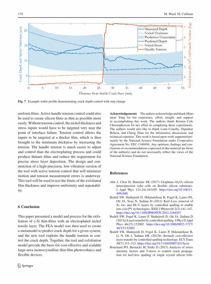
To demonstrate the control capabilities of the han-dle film tension, a similar test was performed but witha larger step change in tension. The profile for thistest is shown in Fig. 7. Again, the metamodel appearsto slightly overpredict the effect of the handle tensionwhile accurately following the trends in the profile. Inthis case, the load change step was approximately 70 Nwhich was predicted to induce a 6 µm change in crackdepth. The actual change in depth was 4.3µm. The dis-crepancy could be caused by a bias in the tension mea-surement system created by unaccounted for friction inthe roller mechanism that is magnified by high tensionloads. Both plots show non-uniformity in the measuredcrack depth profile that is unexplained by the nickelthickness, stress, and handle tension measurements.Therefore, this variation is also not demonstrated in themetamodel prediction. This may be caused by errorsin the measurements or imperfections in the exfolia-tion tool’s motion due to errors in the constraints andmotion of the linear actuator and roller runout.
These results show that while the handle tensioncan be used to effectively influence the crack depth,other factors like the nickel thickness and stress alsohave a strong influence on the resulting crack depthand can produce nonuniformities in the final product.Increasing the uniformity of the nickel will improveresults, but this is difficult to achieve with electro-plating. Since electroplating is inexpensive, accuratelymeasured nonuniformities could be countered by activecontrol of the handle tension to produce cost-effective
123
170 M. Ward, M. Cullinan
Fig. 7 Example wafer profile demonstrating crack depth control with step change
uniform films. Active handle tension control could alsobe used to create silicon films as thin as possible moreeasily.Without tension control, the nickel thickness andstress inputs would have to be targeted very near thepoint of interface failure. Tension control allows theinputs to be targeted at a thicker film, which is thenbrought to the minimum thickness by increasing thetension. The handle tension is much easier to adjustand control than the electroplating process and couldproduce thinner films and reduce the requirement forprecise stress layer deposition. The design and con-struction of a high-precision, low-vibration version ofthe tool with active tension control that will minimizemotion and tension measurement errors is underway.This tool will be used to test the limits of the exfoliatedfilm thickness and improve uniformity and repeatabil-ity.
6 Conclusion
This paper presented a model and process for the exfo-liation of c-Si thin-films with an electroplated nickeltensile layer. The FEA model was then used to createa metamodel to predict crack depth for a given system,and the new tool exploits the handle tension to con-trol the crack depth. Together, the tool and exfoliationmodel provide the basis for cost-effective and scalablelarge-area monocrystalline thin-film photovoltaics andflexible devices.
Acknowledgements Theauthors acknowledge and thankMiao-miao Yang for her experience, effort, insight, and supportin accomplishing this work. The authors thank Kirsten ColeChristopherson for her effort in completing these experiments.The authors would also like to thank Liam Conolly, DipankarBehera, and Cheng Zhao for the informative discussions andtechnical expertise. This work is based upon work supported pri-marily by the National Science Foundation under CooperativeAgreement No. EEC-1160494. Any opinions, findings and con-clusions or recommendations expressed in this material are thoseof the author(s) and do not necessarily reflect the views of theNational Science Foundation.
References
Ahn J, Chou H, Banerjee SK (2017) Graphene-Al2O3-siliconheterojunction solar cells on flexible silicon substrates.J Appl Phys 121(16):163105. https://doi.org/10.1063/1.4981880
Bedell SW, Shahrjerdi D, Hekmatshoar B, Fogel K, Lauro PA,Ott JA, Sosa N, Sadana D (2012) Kerf–Less removal ofSi, Ge, and III–V layers by controlled spalling to enablelow-cost PV technologies. IEEE J Photovolt 2(2):141–147.https://doi.org/10.1109/JPHOTOV.2012.2184267
Bedell SW, Fogel K, Lauro P, Shahrjerdi D, Ott JA, Sadana D(2013a) Layer transfer by controlled spalling. J PhysDApplPhys 46(15):152002. https://doi.org/10.1088/0022-3727/46/15/152002
Bedell SW, Shahrjerdi D, Fogel K, Lauro P, Hekmatshoar B,Li N, Ott J, Sadana DK (2013b) (Invited) cost-effectivelayer transfer by controlled spalling technology. ECS Trans50(7):315–323. https://doi.org/10.1149/05007.0315ecst
Bouchard PO, Bernacki M, Parks D (2013) Analysis of stressintensity factors and T-stress to control crack propaga-tion for kerf-less spalling of single crystal silicon foils.
123

A fracture model for exfoliation of thin silicon films 171
Comput Mater Sci 69:243–250. https://doi.org/10.1016/j.commatsci.2012.10.033
Calvez D, Roqueta F, Jacques S, Bechou L, Ousten Y,Ducret S (2014) Crack propagation modeling in sili-con: a comprehensive thermomechanical finite-elementmodel approach for power devices. IEEE Trans ComponPackag Manuf Technol 4(2):360–366. https://doi.org/10.1109/TCPMT.2013.2293094
Cannon RM, Fisher RM, Evans AG (1985) Decohesion of thinfilms from ceramic substrates. In:MRS proceedings, vol 54.https://doi.org/10.1557/PROC-54-799
Drory MD, Thouless MD, Evans AG (1988) On the decohesionof residually stressed thin films. Acta Metall 36(8):2019–2028
Dross F, Robbelein J,VandeveldeB,VanKerschaver E,Gordon I,Beaucarne G, Poortmans J (2007) Stress-induced large-arealift-off of crystalline Si films. Appl Phys A 89(1):149–152.https://doi.org/10.1007/s00339-007-4195-2
Fortunato E, Barquinha P, Martins R (2012) Oxide semicon-ductor thin-film transistors: a review of recent advances.Adv Mater 24(22):2945–2986. https://doi.org/10.1002/adma.201103228
Janssen G, Abdalla M, van Keulen F, Pujada B, van Ven-rooy B (2009) Celebrating the 100th anniversary of theStoney equation for film stress: developments from poly-crystalline steel strips to single crystal silicon wafers. ThinSolid Films 517(6):1858–1867. https://doi.org/10.1016/j.tsf.2008.07.014
Kim J, Lee M, Shim HJ, Ghaffari R, Cho HR, Son D, JungYH, Soh M, Choi C, Jung S, Chu K, Jeon D, Lee ST, KimJH, Choi SH, Hyeon T, Kim DH (2014) Stretchable siliconnanoribbon electronics for skin prosthesis. Nat Commun5:5747. https://doi.org/10.1038/ncomms6747
Luo J (2004) Young’s modulus of electroplated Ni thin filmfor MEMS applications. Mater Lett 58(17–18):2306–2309.https://doi.org/10.1016/j.matlet.2004.02.044
Masolin A, Bouchard PO, Martini R, Bernacki M (2013)Thermo-mechanical and fracture properties in single-crystal silicon. J Mater Sci 48(3):979–988. https://doi.org/10.1007/s10853-012-6713-7
Mathew L, Jawarani D (2010) Method of forming an elec-tronic device using a separation-enhancing species. USpatent US7749884B2. https://patents.google.com/patent/US7749884/en
Pagliaro M, Ciriminna R, Palmisano G (2008) Flexible solarcells. ChemSusChem 1(11):880–891. https://doi.org/10.1002/cssc.200800127
Pang C, Lee C, Suh KY (2013) Recent advances in flexible sen-sors for wearable and implantable devices. J Appl PolymSci 130(3):1429–1441. https://doi.org/10.1002/app.39461
Pudasaini PR, SharmaM,Ruiz-Zepeda F,AyonAA (2014)Ultra-thin, flexible, hybrid solar cells in sub-ten micrometers sin-gle crystal silicon membrane. In: 2014 IEEE 40th photo-voltaic specialist conference (PVSC). IEEE, pp 0953–0955
Rao RA, Mathew L, Saha S, Smith S, Sarkar D, Garcia R, StoutR, Gurmu A, Onyegam E, Ahn D (2011) A novel low cost25μm thin exfoliated monocrystalline si solar cell technol-ogy. In: 2011 37th IEEE photovoltaic specialists conference(PVSC). IEEE, pp 001504–001507
Shahrjerdi D, Bedell SW (2013) Extremely flexible nanoscaleultrathin body silicon integrated circuits on plastic. NanoLett 13(1):315–320. https://doi.org/10.1021/nl304310x
Shahrjerdi D, Bedell SW, Khakifirooz A, Fogel K, Lauro P,Cheng K, Ott JA, Gaynes M, Sadana DK (2012) Advancedflexible CMOS integrated circuits on plastic enabled bycontrolled spalling technology. In: 2012 IEEE internationalelectron devices meeting (IEDM). IEEE, pp 5–1
Suo Z, Hutchinson JW (1989) Steady-state cracking inbrittle substrates beneath adherent films. Int J SolidsStruct 25(11):1337–1353. https://doi.org/10.1016/0020-7683(89)90096-6
Takei K, Takahashi T, Ho JC, KoH, Gillies AG, Leu PW, FearingRS, Javey A (2010) Nanowire active-matrix circuitry forlow-voltage macroscale artificial skin. Nat Mater 9:821–826. https://doi.org/10.1038/nmat2835
Tanielian M, Lajos RE, Blackstone S (1986) Method ofmaking thin free standing single crystal films USpatent US4582559A. https://patents.google.com/patent/US4582559A/en?oq=+4%2c582%2c559
Thouless MD, Evans AG, Ashby MF, Hutchinson JW(1987) The edge cracking and spalling of brittle plates.Acta Metall 35(6):1333–1341. https://doi.org/10.1016/0001-6160(87)90015-0
Weil R (1970) The origins of stress in electrodeposits. Part 1.Plating 57(12):1231–1237
Xu Y, Blume JA, Shih CF (1993) An interface crack between anorthotropic thin film and substrate. Int J Fract 63(4):369–381
Ying M, Bonifas AP, Lu N, Su Y, Li R, Cheng H, Ameen A,Huang Y, Rogers JA (2012) Silicon nanomembranes for fin-gertip electronics. Nanotechnology 23(34):344004. https://doi.org/10.1088/0957-4484/23/34/344004
Zhai Y, Mathew L, Rao R, Xu D, Banerjee SK (2012) High-performance flexible thin-film transistors exfoliated frombulk wafer. Nano Lett 12(11):5609–5615. https://doi.org/10.1021/nl302735f
Publisher’s Note Springer Nature remains neutral with regardto jurisdictional claims in published maps and institutional affil-iations.
123