Embed Size (px)
Citation preview
A flexoelectric microelectromechanical system on
silicon
Umesh Kumar Bhaskar1+
*, Nirupam Banerjee2+
, Amir Abdollahi1, Zhe Wang
3, Darrell G.
Schlom3,4
, Guus Rijnders2, and Gustau Catalan
1,5*
1 ICN2 – Institut Catala de Nanociencia i Nanotecnologia, CSIC and The Barcelona Institute of
Science and Technology, Campus UAB, 08193 Bellaterra
(Barcelona), Spain.
2 Faculty of Science and Technology and MESA+ Institute for Nanotechnology, University of
Twente, P.O. Box 217, 7500 AE Enschede, The Netherlands
3 Department of Materials Science and Engineering Cornell University, Ithaca, NY 14853, USA
4 Kavli Institute at Cornell for Nanoscale Science, Ithaca, New York 14853, USA
5 ICREA - Institucio Catalana de Recerca i Estudis Avançats, 08010 Barcelona, Spain
KEYWORDS: flexoelectricity, MEMS, nanoscale, piezoelectrics
Flexoelectricity allows a dielectric material to polarize in response to a mechanical bending
moment1, and, conversely, to bend in response to an electric field
2. Compared to piezoelectricity,
flexoelectricity is a weak effect of little practical significance in bulk materials. However, the
roles can be reversed at the nanoscale3. Here, we demonstrate that flexoelectricity is a viable
route to lead-free microelectromechanical and nanoelectromechanical systems (MEMS and
NEMS). Specifically, we have fabricated a silicon compatible thin film cantilever actuator with a
single flexoelectrically active layer of strontium titanate with a figure of merit (curvature divided
by electric field) of 3.33 MV-1
, comparable to that of the state of the art piezoelectric bimorph
cantilevers.
Main
Certain attributes of flexoelectricity point towards a favourable role in micro- and nano-
electromechanical systems (MEMS and NEMS), for example: (i) Flexoelectricity is a universal
phenomenon exhibited by materials of all symmetry groups, and thus flexoelectric devices can in
principle be fabricated from silicon or any of its gate dielectrics in a completely complementary
metal oxide semiconductor (CMOS) compatible environment; (ii) Any (strain) gradient scales
inversely with the material dimension3, thus allowing flexoelectricity to match or even dominate
over piezoelectricity at the nanoscale4, particularly in materials with high dielectric permittivity
, such as ferroelectric thin film5 and composites
6; (iii) High frequency bending resonators
capable of functioning at extreme temperatures can be implemented; (iv) Flexoelectric devices
can be made from simple dielectrics, with a performance that is therefore linear and non-
hysteretic, and (v) A flexoelectric, unlike a piezoelectric bimorph actuator, does not need to be
clamped to an elastic passive layer in order to bend: a single dielectric layer is sufficient to
achieve field-induced bending, and this simplifies device design and removes the risk of
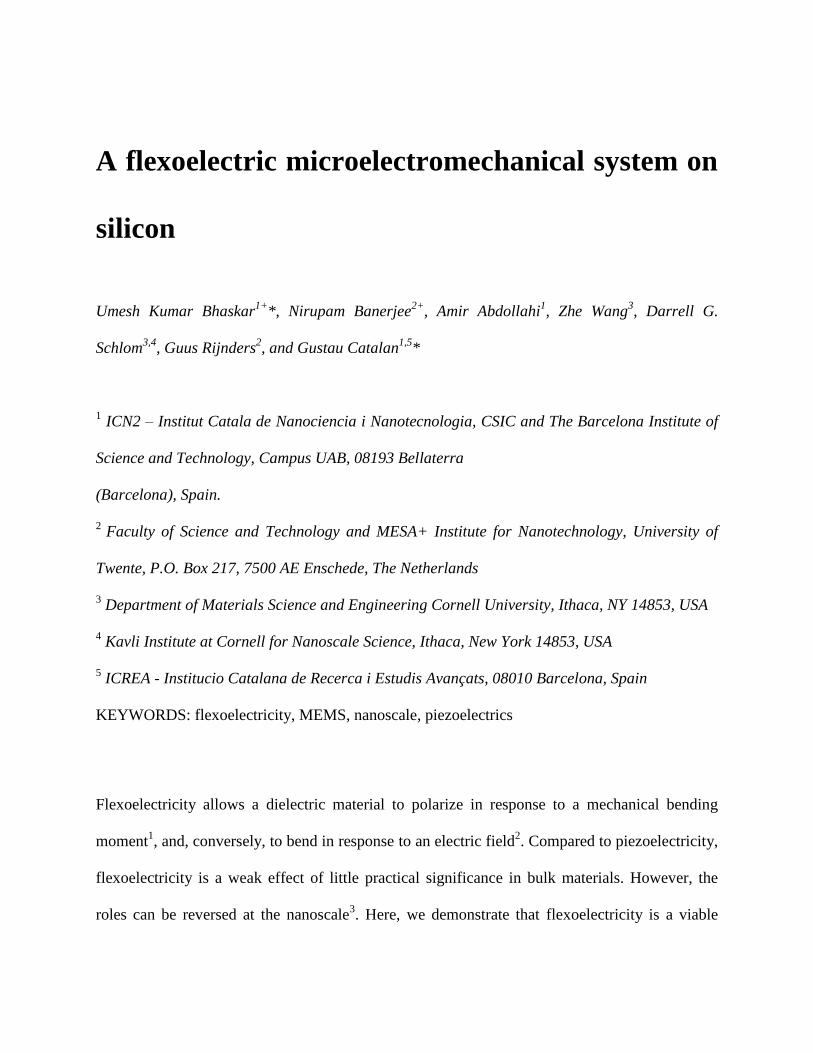
delamination that can exist in standard piezoelectric bimorph actuators (Figure 1).
In contrast, since the materials with the largest piezoelectric coefficients are ferroelectric, piezo-
electric devices can suffer from their intrinsically hysteric nature and nonlinear behaviour at
fields close to the coercive voltage, and in addition their properties are strongly temperature-
dependent: they only work below their Curie temperature. Moreover, the ferroelectrics with
largest piezoelectric coefficients are lead-based7, and lead toxicity poses serious problems for
integration of such devices in biomedical applications, where MEMS-based energy harvesting
devices would otherwise find a natural niche of applications8. In addition, bimorphs can also be
restricted by the mechanical and thermal expansion mismatch between the piezoelectric and
elastic layer, which can lead to progressive deterioration of the bonding between layers.
Despite the advantages offered by nanoscale flexoelectricity, research in this field is still in its
infancy9,10
, and considerable effort is required before it can be established as a viable technology.
On the fundamental front, we need a reliable catalogue of flexoelectric coefficients for all
materials of technological interest, and proof that the magnitude of these coefficients remains
constant at the nanoscale. On the practical front, we need to develop both nanofabrication and
nano-characterization tools suitable for making and measuring flexoelectric nanodevices. This
article addresses both of these issues.
We fabricated all-oxide nanocantilevers (Figure 2(a)) as capacitor structures consisting of a
strontium titanate (SrTiO3) active layer sandwiched between two layer of strontium ruthenate
(SrRuO3) for the top and bottom electrode; the complete capacitor stack (see Figure S1 and
Figure S2) is epitaxially grown on a buffer of SrTiO3 deposited by molecular beam epitaxy
(MBE) on Si, which is currently an established template system for incorporating other epitaxial
oxide films on Si11
. Fabrication details are provided in the methods section. The centrosymmetric
lattice of room temperature SrTiO3 ensures that any measured bending moment arises purely
from flexoelecticity; room temperature paraelectricity in SrTiO3 is also confirmed by its linear
and non-hysteretic mechanical response as a function of electric field; for comparison, in the
supplementary materials (See Figure S3) we show the characteristic butterfly-shape hysteresis
loop response of a ferroelectric lead zirconium titanate (PZT) cantilever grown by similar
methods on silicon. SrTiO3 is also currently the only (bulk) material for which the theoretical and
experimental values, measured using the direct method are of the same order of magnitude12
,
providing a good reference for testing two important questions: (i) whether the bulk flexoelectric
coefficients retain their bulk value in thin films and (ii) whether the coefficients measured by us
via the inverse method (actuator mode) are the same as those measured in bulk by the direct
method (sensor mode) –something that is definitely true for piezoelectrics but is not obvious in
flexoelectricity, where this question has been controversial13
.
The most popular method currently used to characterize flexoelectric coefficients involves
dynamically bending a cantilever and using lock-in techniques to instantaneously measure the
charge generated by the bending. We refer to this as the direct method, and it has been employed
on a variety of materials, including perovskite ceramics14
, single crystals12
, and even polymers15
.
Its drawback is the difficulty of miniaturizing mechanical bending appliances down to the
nanoscale. But, while direct flexoelectricity measures the polarization induced by bending, a
converse or inverse effect also exists whereby polarizing a sample causes it to bend2,13,16,17,18
.
The “inverse method” thus involves the application of an electric field to a cantilever or plate-
shaped material, and measuring the induced bending16,18
. The curvature (k) induced via
flexoelectricity (µ) is related to the flexural rigidity (D) of the plate and the applied voltage (V)
by 9 :
. (1)
The flexural rigidity (D) of a cantilever is
, where E is the young´s modulus, ν is the
Poisson ratio, and t is the thickness. Hence, the flexoelectrically induced curvature scales as
the cube of the cantilever thickness, i.e., the voltage-induced bending multiplies by a factor of 8
–almost an order of magnitude- every time the thickness is halved. The inverse scaling of with
the Young´s modulus also makes it pertinent to characterizing soft materials, which are expected
to display giant electromechanical couplings19
. On the practical side, achieving converse
flexoelectricity only requires the fabrication of planar capacitive cantilevers, and we demonstrate
that this requirement can be readily realized using existing MEMS techniques. Thus, inverse
flexoelectricity is an optimum route to exploring and exploiting the flexoelectricity of
nanodevices.
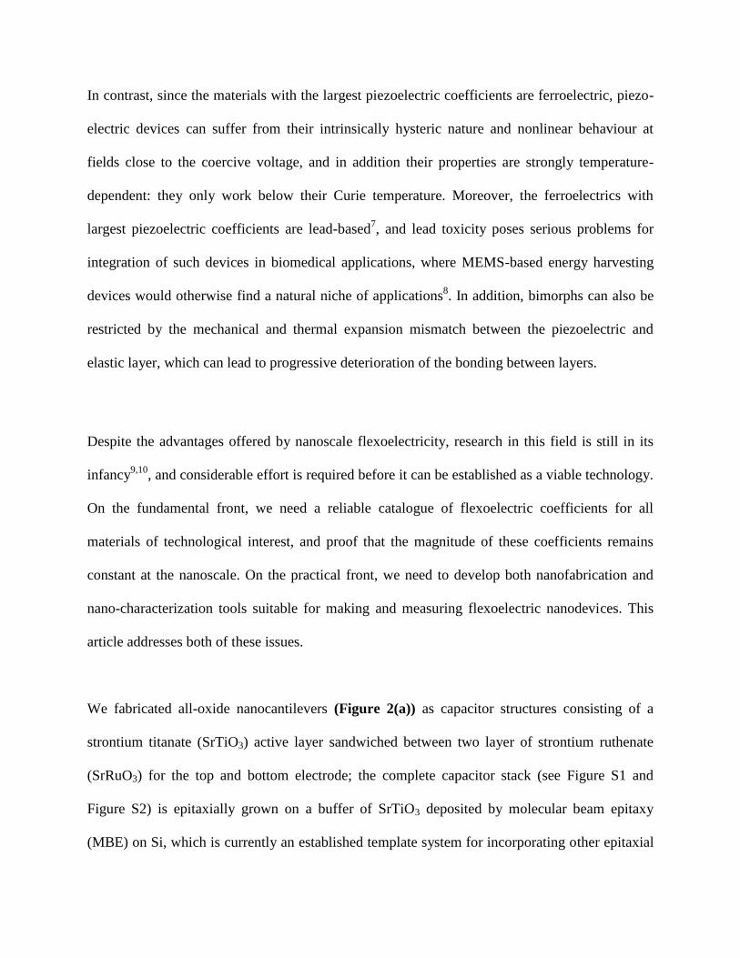
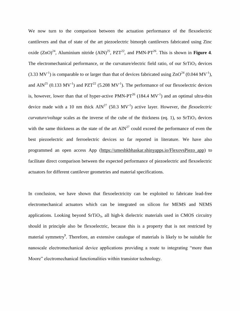
The observation of cantilever oscillations induced by an applied alternate voltage (Vac) was made
using a commercial digital holographic microscope20,21
(DHM) (schematically illustrated in
Figure 2(b) and 2(c)) working in stroboscopic mode. The Fourier-filtered first harmonic
displacement induced in the 16 x 40 um SrTiO3 cantilever plate is plotted as a function of the AC
excitation at 100 KHz and just above resonance (320 KHz) in Figure 3(a) and 3(b) respectively
(the unfiltered response at 100 KHz is shown in Figure S4). The curvature was calculated from
the Fourier-filtered displacement22
. In order to probe the dynamics further, the cantilever was
excited with the same bias of 1 V but over a range of different sinusoidal frequencies (Figure
3(c)). The observed resonance frequency ~310 kHz corresponds quite well with the analytical
estimation based on the geometry of the cantilever (see Figure S5), while the phase corresponds
to the lag between the waveform of the excitation signal (voltage) and that of the flexoelectric
response (deflection).
The first harmonic curvature measured as a function of applied AC field at ~100 KHz is plotted
in Figure 3(d) and shows the expected linear behavior for a flexoelectric actuator. In order to
demonstrate the stability of the measurements as a function of the frequency, we also include a
complete curvature vs field measurement made at 10 KHz in figure S6. The value of the
flexoelectric coefficient µeff calculated from the slope of curvature vs voltage using Equation 1
yields µeff ~ 4.6 nC/m. This is an effective flexoelectric coefficient involving a geometry-
dependent combination of the flexoelectric tensor components. Calculations using a self-
consistent continuum model of flexoelectricity16
under the assumption that the ratio between µ11
and µ12 remains the same as in bulk12
yield µ12 ~ 4.1 nC/m. This is comparable to the µ12 for bulk
SrTiO3 (100) crystals measured by the direct method (µ12 ~ 7 nC/m)12
, particularly when
factoring in the smaller relative permittivity of our SrTiO3 thin film, which is ~four times smaller
compared to that of bulk single crystals. Indeed, the quantity of physical significance9 is the
flexocoupling ratio f =
, which we found to be 6 V for SrTiO3 nanocantilevers, in good
agreement with the estimate proposed by Kogan of 1-10 V for ionic solids1, and comparable to
the value found for other perovskites such as lead magnesium niobate-lead titanate (PMN-PT)23
.
The similarity of the coefficients measured by inverse and direct methods also provides
experimental validation that flexoelectric devices will display the same coupling constant for
operation as sensor and actuator13
.
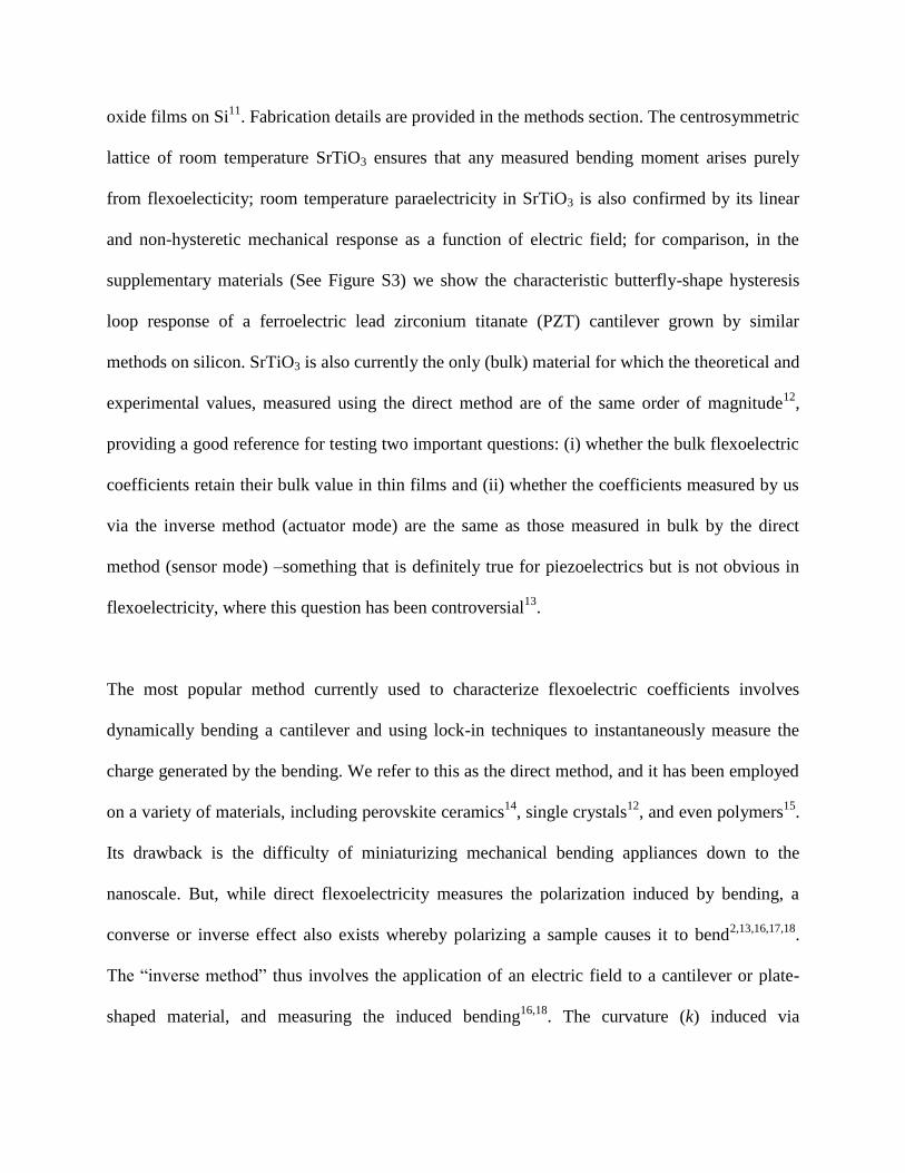
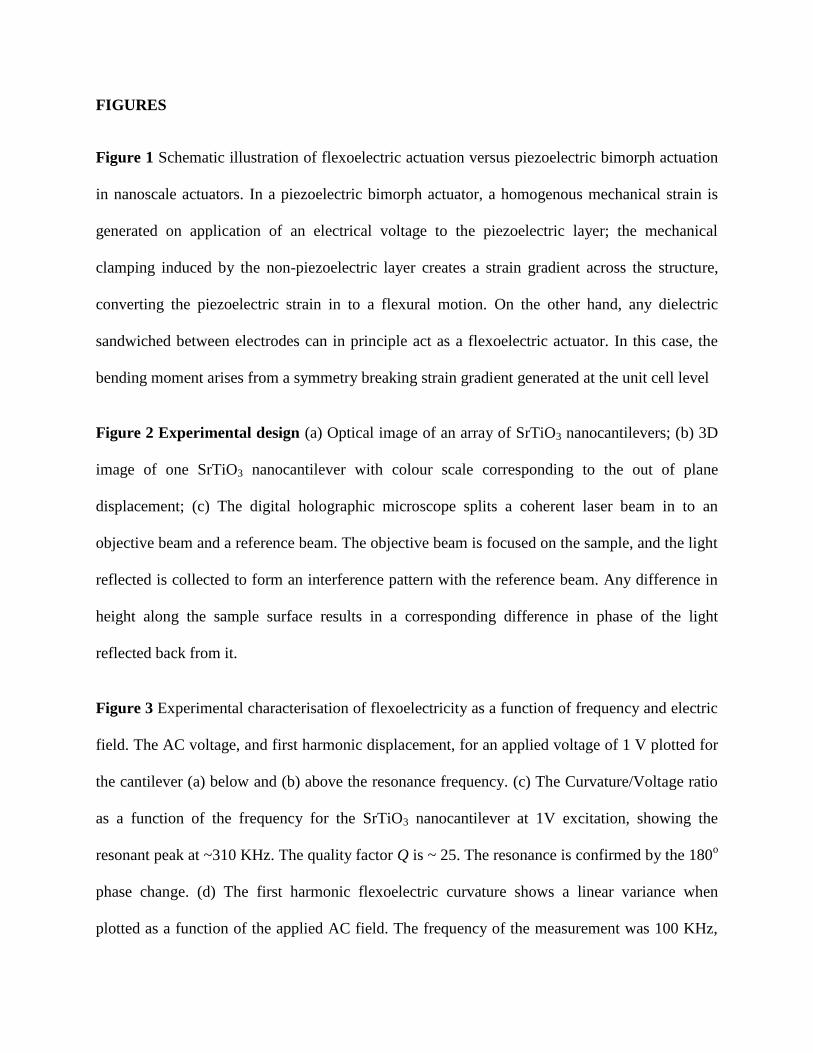
We now turn to the comparison between the actuation performance of the flexoelectric
cantilevers and that of state of the art piezoelectric bimorph cantilevers fabricated using Zinc
oxide (ZnO)24
, Aluminium nitride (AlN)25
, PZT22
, and PMN-PT26
. This is shown in Figure 4.
The electromechanical performance, or the curvature/electric field ratio, of our SrTiO3 devices
(3.33 MV-1
) is comparable to or larger than that of devices fabricated using ZnO24
(0.044 MV-1
),
and AlN25
(0.133 MV-1
) and PZT22
(5.208 MV-1
). The performance of our flexoelectric devices
is, however, lower than that of hyper-active PMN-PT26
(184.4 MV-1
) and an optimal ultra-thin
device made with a 10 nm thick AlN27
(50.3 MV-1
) active layer. However, the flexoelectric
curvature/voltage scales as the inverse of the cube of the thickness (eq. 1), so SrTiO3 devices
with the same thickness as the state of the art AlN27
could exceed the performance of even the
best piezoelectric and ferroelectric devices so far reported in literature. We have also
programmed an open access App (https://umeshkbhaskar.shinyapps.io/FlexovsPiezo_app) to
facilitate direct comparison between the expected performance of piezoelectric and flexoelectric
actuators for different cantilever geometries and material specifications.
In conclusion, we have shown that flexoelectricity can be exploited to fabricate lead-free
electromechanical actuators which can be integrated on silicon for MEMS and NEMS
applications. Looking beyond SrTiO3, all high-k dielectric materials used in CMOS circuitry
should in principle also be flexoelectric, because this is a property that is not restricted by
material symmetry9. Therefore, an extensive catalogue of materials is likely to be suitable for
nanoscale electromechanical device applications providing a route to integrating “more than
Moore” electromechanical functionalities within transistor technology.
FIGURES
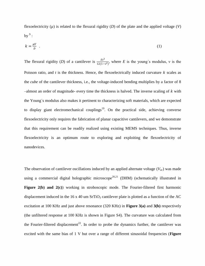
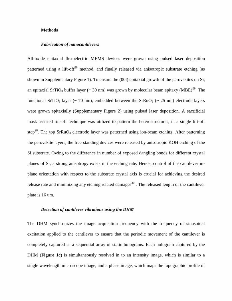
Figure 1 Schematic illustration of flexoelectric actuation versus piezoelectric bimorph actuation
in nanoscale actuators. In a piezoelectric bimorph actuator, a homogenous mechanical strain is
generated on application of an electrical voltage to the piezoelectric layer; the mechanical
clamping induced by the non-piezoelectric layer creates a strain gradient across the structure,
converting the piezoelectric strain in to a flexural motion. On the other hand, any dielectric
sandwiched between electrodes can in principle act as a flexoelectric actuator. In this case, the
bending moment arises from a symmetry breaking strain gradient generated at the unit cell level
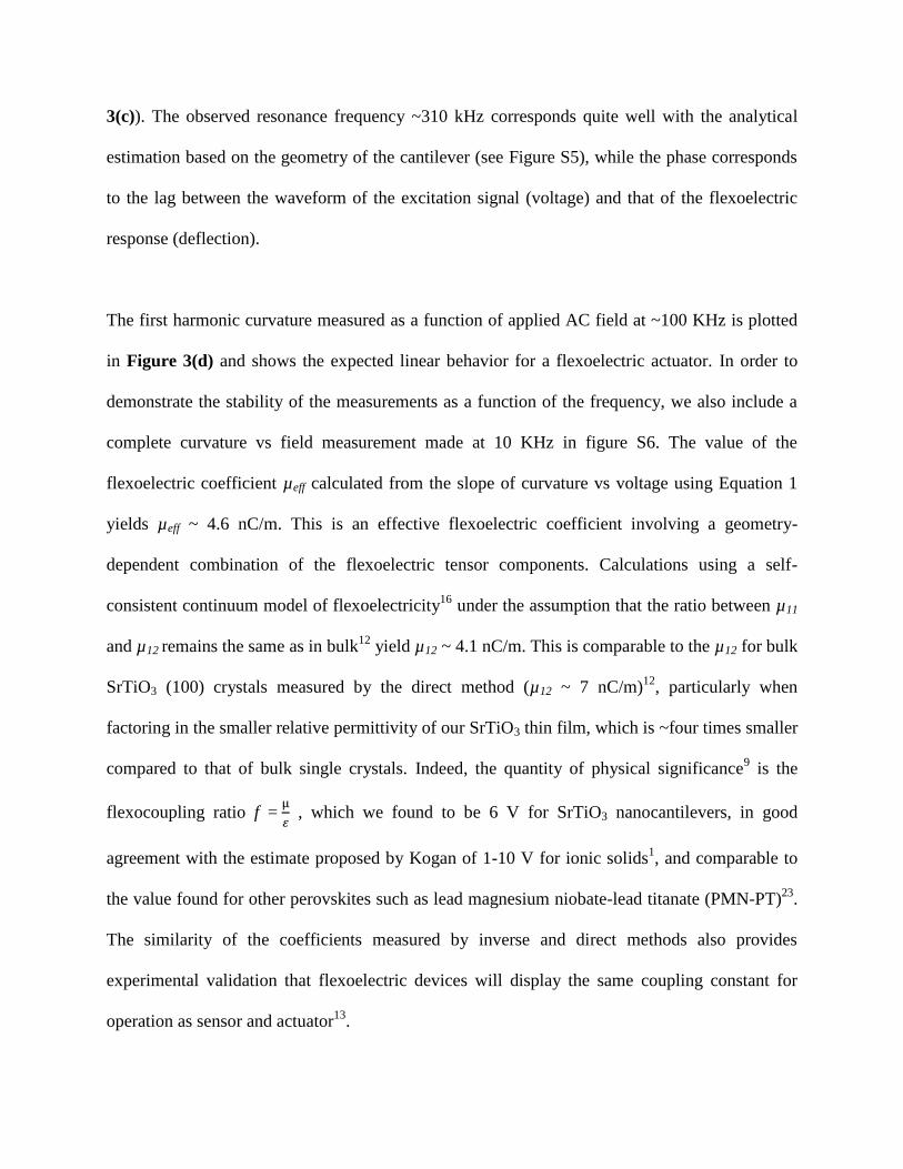
Figure 2 Experimental design (a) Optical image of an array of SrTiO3 nanocantilevers; (b) 3D
image of one SrTiO3 nanocantilever with colour scale corresponding to the out of plane
displacement; (c) The digital holographic microscope splits a coherent laser beam in to an
objective beam and a reference beam. The objective beam is focused on the sample, and the light
reflected is collected to form an interference pattern with the reference beam. Any difference in
height along the sample surface results in a corresponding difference in phase of the light
reflected back from it.
Figure 3 Experimental characterisation of flexoelectricity as a function of frequency and electric
field. The AC voltage, and first harmonic displacement, for an applied voltage of 1 V plotted for
the cantilever (a) below and (b) above the resonance frequency. (c) The Curvature/Voltage ratio
as a function of the frequency for the SrTiO3 nanocantilever at 1V excitation, showing the
resonant peak at ~310 KHz. The quality factor Q is ~ 25. The resonance is confirmed by the 180o
phase change. (d) The first harmonic flexoelectric curvature shows a linear variance when
plotted as a function of the applied AC field. The frequency of the measurement was 100 KHz,
well below the resonant frequency amplification and close to the static performance calculated
from the fit in (c).
Figure 4 Comparison of the performance of flexoelectric SrTiO3 with that of the state of the art
piezoelectric bimorphs. The ratio of Curvature/Electric field is compared for a flexoelectric
SrTiO3, and piezoelectric devices fabricated from ZnO24
, AlN25,27
, PZT22
, and PMN-PT26
. For all
materials, we quote the intrinsic response measured out of resonance.
ACKNOWLEDGMENT
The work at ICN2 was funded by an ERC Starting Grant from the EU (Project No. 308023), a
National Plan grant from Spain (FIS2013-48668-C2-1-P) and the Severo Ochoa Excellence
programme. The work at Cornell University was supported by the National Science Foundation
(Nanosystems Engineering Research Center for Translational Applications of Nanoscale
Multiferroic Systems) under grant number EEC-1160504. The authors are grateful to discussions
with Etienne Cuche, Jerome Parent, Eduardo Solanas and Yves Emery.
Author Contributions
+Both authors contributed equally.
G.C and U.B conceived and designed the experiments; N.B designed and made the cantilevers
under the supervision of G.R; U.B performed and analysed the inverse flexoelectric
characterizations under the supervision of G.C; A.A performed the self-consistent continuum
modelling and simulations; Z.W performed the Molecular beam epitaxy growth of the template
layer under the supervision of D.S; U.B. and G. C. wrote the paper with the help of all other
authors. All authors discussed the results, commented on the manuscript and have given their
approval to the final version of the manuscript.
Additional information
Supplementary information accompanies this paper at www.nature.com/naturenanotechnology.
Reprints and permission information is available online at
http://npg.nature.com/reprintsandpermissions/.
Correspondence and requests for materials should be addressed to U.B and G.C.
REFERENCES
1. Kogan, S. Piezoelectric effect during inhomogeneous deformation and acoustic scattering
of carriers in crystals. Sov. Phys. Solid State 5, 2069–2079 (1964).
2. Bursian, E. & Trunov, N. Nonlocal piezoelectric effect. Sov. Phys. Solid State 16, 760–
762 (1974).
3. Gregg, J. M. Stressing Ferroelectrics. Science 336, 41–42 (2012).
4. Majdoub, M., Sharma, P. & Çağin, T. Dramatic enhancement in energy harvesting for a
narrow range of dimensions in piezoelectric nanostructures. Phys. Rev. B 78, 121407
(2008).
5. Lee, D. et al. Giant flexoelectric effect in ferroelectric epitaxial thin films. Phys. Rev. Lett.
107, 057602 (2011).
6. Cross, L. Flexoelectric effects: Charge separation in insulating solids subjected to elastic
strain gradients. J. Mater. Sci. 41, 53–63 (2006).
7. Cross, E. Lead-free at last. Nature 32, 24–25 (2004).
8. Dreyfus, R. et al. Microscopic artificial swimmers. Nature 437, 862–865 (2005).
9. Zubko, P., Catalan, G. & Tagantsev, A. K. Flexoelectric Effect in Solids. Annu. Rev.
Mater. Res. 43, 387–421 (2013).
10. Biancoli, A., Fancher, C. M., Jones, J. L. & Damjanovic, D. Breaking of macroscopic
centric symmetry in paraelectric phases of ferroelectric materials and implications for
flexoelectricity. Nat. Mater. 14, 224–229 (2014).
11. Cross, L. Flexoelectric effects: Charge separation in insulating solids subjected to elastic
strain gradients. J. Mater. Sci. 41, 53–63 (2006).
12. Zubko, P., Catalan, G., Buckley, A., Welche, P. & Scott, J. Strain-Gradient-Induced
Polarization in SrTiO3 Single Crystals. Phys. Rev. Lett. 99, 167601 (2007).
13. Breger, L., Furukawa, T. & Fukada, E. Bending piezoelectricity in polyvinylidene
fluoride. Jpn. J. Appl. Phys. 15, 2239–40 (1976).
14. Tagantsev, A. K. & Yurkov, A. S. Flexoelectric effect in finite samples. J. Appl. Phys.
112, 044103 (2012).
15. Bursian, E. & Zaikovskii, O. I. Changes in curvature of ferroelectric film due to
polarization. Sov. Phys. Solid State 10, 1121 (1968).
16. Abdollahi, A., Peco, C., Millán, D., Arroyo, M., & Arias, I.. Computational evaluation of
the flexoelectric effect in dielectric solids. J. Appl. Phys 116, 093502 (2014).
17. Zalesskii, V. G. & Rumyantseva, E. D. Converse flexoelectric effect in the SrTiO3 single
crystal. Phys. Solid State 56, 1352–1354 (2014).
18. Deng, Q., Liu, L. & Sharma, P. Electrets in soft materials: Nonlinearity, size effects, and
giant electromechanical coupling. Phys. Rev. E, Soft Matter Phys. 90, 1–7 (2014).
19. Baek, S.-H. & Eom, C.-B. Epitaxial integration of perovskite-based multifunctional oxides
on silicon. Acta Mater. 61, 2734–2750 (2013).
20. Cotte, Y., Toy, F., Jourdain, P. & Pavillon, N. Marker-free phase nanoscopy. Nat.
Photonics 7, 113–117 (2013).
21. Colomb, T., Krivec, S. & Hutter, H. Digital holographic reflectometry. Opt. Express 21,
12643–12650 (2013).
22. Dekkers, M. et al. The significance of the piezoelectric coefficient d31eff determined from
cantilever structures. J. Micromechanics Microengineering 23, 025008 (2013).
23. Narvaez, J. & Catalan, G. Origin of the enhanced flexoelectricity of relaxor ferroelectrics.
Appl. Phys. Lett. 104, 162903 (2014).
24. Wang, P., Du, H., Shen, S., Zhang, M. & Liu, B. Preparation and characterization of ZnO
microcantilever for nanoactuation. Nanoscale Res. Lett. 7, 176 (2012).
25. Doll, J. C., Petzold, B. C., Ninan, B., Mullapudi, R. & Pruitt, B. L. Aluminum nitride on
titanium for CMOS compatible piezoelectric transducers. Journal of Micromechanics and
Microengineering 20, 025008 (2009).
26. Baek, S. H. et al. Giant Piezoelectricity on Si for Hyperactive MEMS. Science 334, 958–
961 (2011).
27. Zaghloul, U. & Piazza, G. 10-25 NM piezoelectric nano-actuators and NEMS switches for
millivolt computational logic. Proc. IEEE Int. Conf. Micro Electro Mech. Syst. 233–236
(2013). doi:10.1109/MEMSYS.2013.6474220
Methods
Fabrication of nanocantilevers
All-oxide epitaxial flexoelectric MEMS devices were grown using pulsed laser deposition
patterned using a lift-off28
method, and finally released via anisotropic substrate etching (as
shown in Supplementary Figure 1). To ensure the (00l) epitaxial growth of the perovskites on Si,
an epitaxial SrTiO3 buffer layer (~ 30 nm) was grown by molecular beam epitaxy (MBE)29
. The
functional SrTiO3 layer (~ 70 nm), embedded between the SrRuO3 (~ 25 nm) electrode layers
were grown epitaxially (Supplementary Figure 2) using pulsed laser deposition. A sacrificial
mask assisted lift-off technique was utilized to pattern the heterostructures, in a single lift-off
step28
. The top SrRuO3 electrode layer was patterned using ion-beam etching. After patterning
the perovskite layers, the free-standing devices were released by anisotropic KOH etching of the
Si substrate. Owing to the difference in number of exposed dangling bonds for different crystal
planes of Si, a strong anisotropy exists in the etching rate. Hence, control of the cantilever in-
plane orientation with respect to the substrate crystal axis is crucial for achieving the desired
release rate and minimizing any etching related damages30
. The released length of the cantilever
plate is 16 um.
Detection of cantilever vibrations using the DHM
The DHM synchronizes the image acquisition frequency with the frequency of sinusoidal
excitation applied to the cantilever to ensure that the periodic movement of the cantilever is
completely captured as a sequential array of static holograms. Each hologram captured by the
DHM (Figure 1c) is simultaneously resolved in to an intensity image, which is similar to a
single wavelength microscope image, and a phase image, which maps the topographic profile of
the sample. The phase images calculate the topography based on the path difference of light
reflected by the surface compared to a specified reference frame; by placing this reference on the
base of the cantilever, each phase image provides us with the full profile –including the
curvature– of the cantilever. By its nature, the measurement is insensitive to any voltage induced
homogenous expansions or deformations, and only records voltage induced changes in the slope
and curvature of the cantilever. The periodic displacement in response to an applied AC
excitation was found to contain both first harmonic (1ω) and second harmonic contributions
(2ω). In order to get the strength of purely the flexoelectric response (which is linearly
proportional to the field and therefore a first harmonic oscillation) Fourier filtering or harmonic
regression was employed to quantify the 1ω bending.
Self-consistent continuum model of flexoelectricity
By employing a self-consistent continuum model of flexoelectricity16
, we perform simulations
of the multilayer cantilever beam under the application of an electric field. The aspect ratio of the
beam is fixed to L/h = 10, where L and h are the length and height of the beam. A larger aspect
ratio leads to almost identical results. The electrical potential is fixed to zero on the top electrode
and we constrain the electric potential on the bottom electrode to a constant value, generating the
same magnitude of the applied electric field as in experiments. The material parameters are
chosen according to the composition of the multilayer cantilever. Given that there is not yet a
universal consensus regarding the size, or even the sign, of the flexoelectric coefficients for any
material, we consider µ12 = −10µ11, a limiting case reported from the direct measurement on
STO12
. Simulation results show that the cantilever is deflected under the applied electrical load,

supporting the experimental observations that a cantilever beam can deform as an
electromechanical actuator due to flexoelectricity.
28. Banerjee, N., Koster, G. & Rijnders, G. Submicron patterning of epitaxial PbZr0.52Ti0.48O3
heterostructures. Appl. Phys. Lett. 102, 142909 (2013).
29. Warusawithana, M. P. et al. A ferroelectric oxide made directly on silicon. Science 324,
367–370 (2009).
30. Banerjee, N., Houwman, E. P., Koster, G. & Rijnders, G. Fabrication of piezodriven,
free-standing, all-oxide heteroepitaxial cantilevers on silicon. Apl Mater. 2, 096103 (2014)
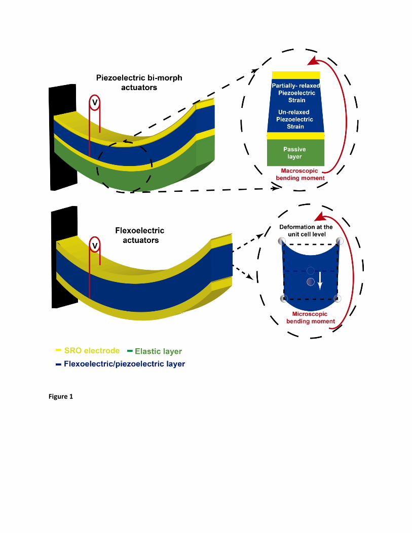
Figure 1
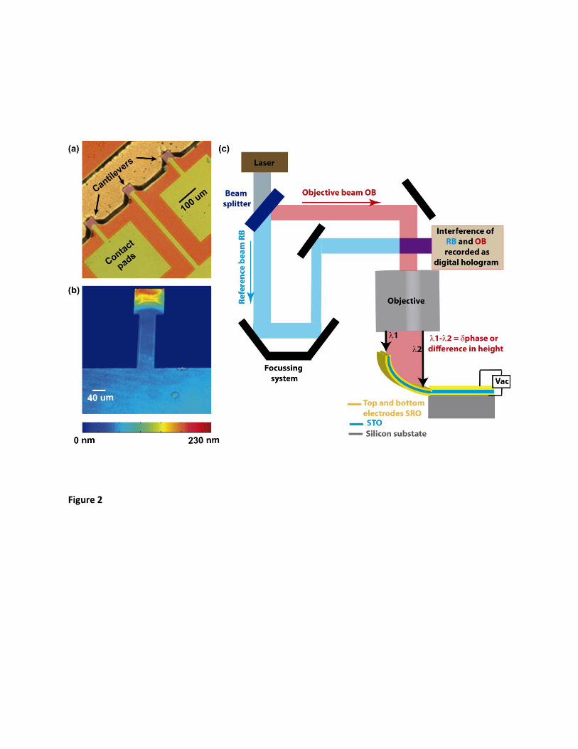
Figure 2
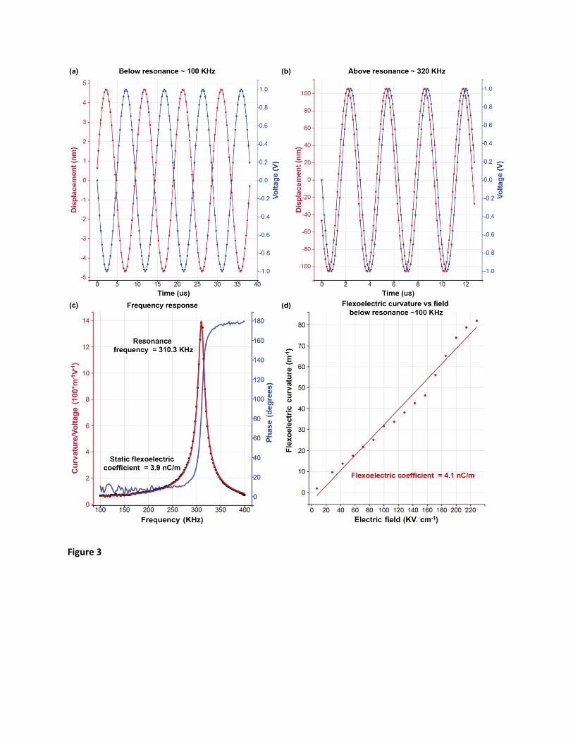
Figure 3
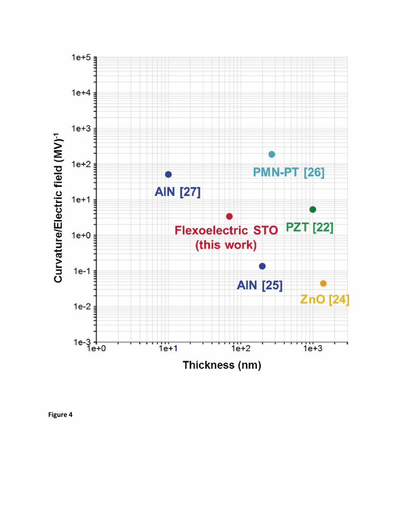
Figure 4