Embed Size (px)
DESCRIPTION
A Five-Level Inverter Topology with Single-DC Supply by Cascading a Flying Capacitor
Citation preview
IEEE TRANSACTIONS ON POWER ELECTRONICS, VOL. 27, NO. 8, AUGUST 2012 3505
A Five-Level Inverter Topology with Single-DCSupply by Cascading a Flying Capacitor
Inverter and an H-BridgeP. Roshankumar, Student Member, IEEE, P. P. Rajeevan, K. Mathew, Student Member, IEEE,
K. Gopakumar, Fellow, IEEE, Jose I. Leon, Member, IEEE, and Leopoldo G. Franquelo, Fellow, IEEE
Abstract—In this paper, a new three-phase, five-level invertertopology with a single-dc source is presented. The proposed topol-ogy is obtained by cascading a three-level flying capacitor inverterwith a flying H-bridge power cell in each phase. This topology hasredundant switching states for generating different pole voltages.By selecting appropriate switching states, the capacitor voltagescan be balanced instantaneously (as compared to the fundamen-tal) in any direction of the current, irrespective of the load powerfactor. Another important feature of this topology is that if anyH-bridge fails, it can be bypassed and the configuration can stilloperate as a three-level inverter at its full power rating. This fea-ture improves the reliability of the circuit. A 3-kW induction motoris run with the proposed topology for the full modulation range.The effectiveness of the capacitor balancing algorithm is tested forthe full range of speed and during the sudden acceleration of themotor.
Index Terms—Flying capacitor (FC), H-bridge, induction motordrive, multilevel inverter.
I. INTRODUCTION
MULTILEVEL inverters have changed the face ofmedium- and high-voltage drives [1], [2]. The most
popular topologies of multilevel converters are the neutral-point-clamped inverter (NPC) [3], the flying capacitor inverter(FC) [4], and the cascaded H-bridge (CHB) inverter [5]. Eachone of these inverters has its own merits and demerits [1]. In theNPC inverter [3], multiple dc sources are generated by splitting asingle-dc bus voltage using capacitor banks. This configurationhas large number of clamping diodes and presents the problemof dc bus capacitor unbalance especially with high number ofvoltage levels [6], [7]. An interesting work for balancing capac-itors in NPC inverter that can be operated in limited modula-tion range has been presented in [8]. A pulse-width modulation(PWM) control scheme to balance the dc link capacitor volt-ages of the NPC inverter, connected in cascade with a two-level
Manuscript received September 15, 2011; revised September 26, 2011;accepted January 16, 2012. Date of current version April 20, 2012. Recom-mended for publication by Associate Editor P. Barbosa.
P. Roshankumar, P. P. Rajeevan, K. Mathew, and K. Gopakumar are withthe Centre for Electronics Design and Technology, Indian Institute of Science,Bangalore 560012, India (e-mail: [email protected]; [email protected]; [email protected]; kgopa@ cedt.iisc.ernet.in).
J. I. Leon and L. G. Franquelo are with the Department of Electronics Engi-neering, University of Seville, 41004 Seville, Spain (e-mail: [email protected];[email protected]).
Digital Object Identifier 10.1109/TPEL.2012.2185714
inverter to realize a five level inverter structure for an open-endwinding induction motor, is proposed in [9].
The concept of FC inverter was introduced first in 1992 [4].In this configuration, multiple capacitors of different voltagemagnitudes are used to generate multiple voltage levels. Theadvantages include modularity, lack of clamping diodes, lackof problems like unbalance in the split dc -link capacitors, etc.Also, as in the NPC case, single supply can be used to generatemultiple pole voltage levels. Many strategies for balancing thecapacitor voltages have evolved over time [10], [11]. However,generating more voltage levels in a FC inverter requires largernumber of capacitors. Interesting derivatives of this configura-tion have been presented in [12] and [13], where more levelshave been achieved by cross connecting the capacitors usingadditional switches. Operation of FC inverter with improved re-liability has been presented in [18], where additional circuitry isprovided to bypass the faulty cell. However, in this scheme, thedevices have to be sufficiently overrated to operate at full powerlevel when the faulty cell is bypassed. The operation of FC in-verter with asymmetrical capacitor voltages to generate morevoltage levels has been presented in [15]. In this configuration,the number of voltage levels that can be achieved depends onthe modulation index and the power factor.
The multilevel CHB inverter with isolated supplies presentedin [5] has many advantages compared to the NPC and FC topolo-gies. The CHB configuration does not require clamping diodesand the input power is distributed among different input sourcesthat makes it more suitable for certain applications [16]. Oneadditional advantage of the CHB converter is that if any de-vice fails in the H-bridges, the inverter can still be operatedat reduced power level and, hence, this configuration is faulttolerant to some extent [17], [18]. The concept of using CHBswith capacitors and their voltage balancing has been introducedin [19] and [20]. The advantages include more redundant states,better voltage balancing, lack of clamping diodes, and fault tol-erant operational ability by bypassing the faulty H-bridge cells.This configuration is especially suitable for applications likeSTATCOM. DC-voltage ratio control strategy for a CHB con-verter fed with a single-dc source is presented in [21]. Withthis control strategy, a higher number of levels in output voltagewaveform can be achieved with capacitor voltage balancing ina limited range of load power factor. This scheme is very muchsuitable for grid-connected applications. A multilevel config-uration with improved reliability has been presented in [22]and [23].
0885-8993/$31.00 © 2012 IEEE

3506 IEEE TRANSACTIONS ON POWER ELECTRONICS, VOL. 27, NO. 8, AUGUST 2012
Fig. 1. Proposed three-phase power circuit formed by the connection of a three-phase flying capacitor inverter with H-bridges in series.
Many other multilevel inverter configurations have been de-veloped based on the three conventional (NPC, FC, and CHB)topologies. A configuration in which two-level inverter is cas-caded with multiple H-bridges has been presented in [24], wheremore voltage levels can be generated. New multilevel inverterconfigurations for open-end winding induction motors, formedby cascading two-level inverters and capacitor-fed H-bridgesare given in [25] and [26].
Five-level active neutral point clamped (ANPC) invertertopology [27] is another configuration, which is a hybrid ofFC topology and NPC configuration. This five-level ANPCconverter is being commercialized by ABB as the ACS2000(up to 1.6 MW). The configuration presented in [28] intro-duces the concept of integrating the cross-connected intermedi-ate level [29] and the ANPC configuration to form a hybrid con-figuration. A hybrid derivative of the ANPC configuration andCHB has been presented in [30]. Derivatives of CHB where dif-ferent devices [Integrated Gate-Commutated Thyristor (IGCT)and insulated gate bipolar transistor (IGBT)] are used in sucha way that the IGCT would switch at fundamental frequencyand IGBT would switch at carrier frequency has been presentedin [31]. The concept of a hybrid cascade converter topology withseries-connected symmetrical and asymmetrical diode-clampedH-bridge cells has been presented in [32]. The hybrid clampedmultilevel inverter topology [33] is a hybrid of NPC topologyand FC topology, which does not have neutral point fluctuation.
The multilevel inverter proposed in this paper is a cascadedtopology consisting of three-level FC inverters and capacitor-fed H-bridges, in which balancing of the capacitor voltages arepossible independently of the load power factor.
II. PROPOSED POWER CIRCUIT
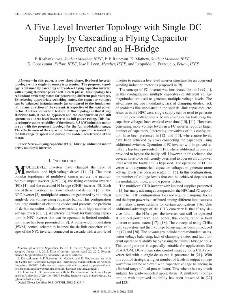
As shown in Fig. 1, the proposed topology has a three-levelFC inverter with dc bus voltage of VDC and FC voltage equal toVDC /2, which can generate voltages of 0, VDC /2, and VDC withrespect to point 0. A capacitor-fed H-bridge is cascaded to eachphase of the inverter. The voltage across the H-bridge capacitorhas to be maintained at VDC /4. This combination can producevoltage levels of 0, VDC /4, VDC /2, 3VDC /4, VDC , −VDC /4, and5VDC /4. Out of these, the voltages −VDC /4 and 5VDC /4 arenot used in the proposed inverter as they do not have redundantswitching states to balance the capacitor voltages. The switch-
ing states of the useful voltage levels and their effects on thecapacitor voltages based on the current direction are given inTable I.
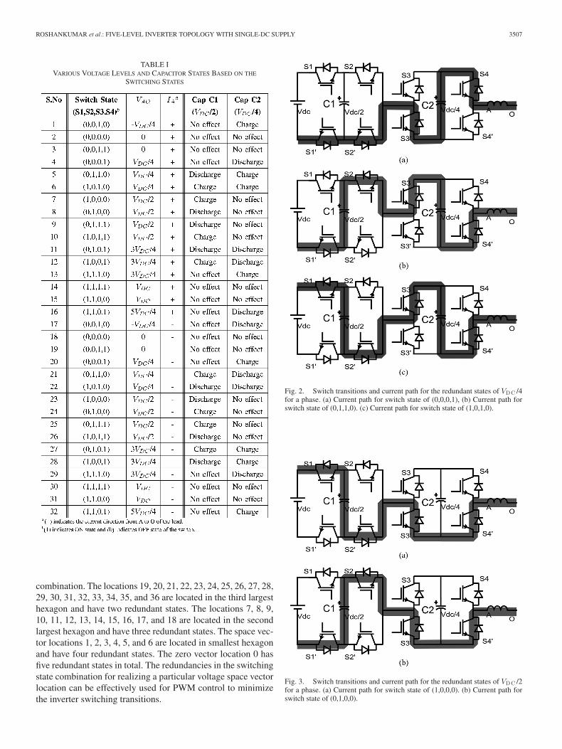
The capacitor voltages remain unaffected while producingthe voltages VDC and 0. The capacitors can either be chargedor discharged in any direction of the current for the voltagesVDC /4, VDC /2, and 3VDC /4 as shown in Figs. 2–4, respectively.In each phase, the switches S1, S2, S3, S4 and S1′, S2′, S3′, S4′
are operated in complementary manner. The output voltage isbased on the switching states that decide the path of the currentflow.
For voltage levels of VDC /4 and 3VDC /4, there are three redun-dant states. By switching between these three states the capaci-tors C1 and C2 can be charged or discharged for any direction ofthe current. The voltage level of VDC /2 has two redundant states.By switching between them, C1 can be charged or dischargedbased on the current direction. When VDC /2 is applied, the C2is not affected. As the capacitors can be either charged or dis-charged by switching between the redundant states, based on thecurrent direction, quick capacitor voltage balancing is possible,irrespective of the load power factor. To maintain the capacitorvoltages at a fixed value, the capacitor voltages are sampled atregular intervals and a hysteresis controller is used to switchbetween the redundant states based on the current direction tobalance the capacitor voltages.
Each pole can generate one of the five voltage levels 0, VDC /4,VDC /2, 3VDC /4, and VDC . The effective voltage space vectorformed based on the three-phase pole voltages is given by
VSV = VAO + VBO � 120◦ − VCO � 120◦ (1)
where VSV is the voltage space vector and VAO , VBO , and VCOare the pole voltages in the three phases A, B, and C, respectively.
The five-level space vector diagram obtained for the com-binations of the pole voltages of the three phases is shown inFig. 5. There are 61 voltage vector locations possible for thefive-level space vector structure. Many of the voltage vector lo-cations have redundant switching state combinations of the polevoltages of three phases. The switching state combinations fora space vector sector of 60◦ interval (as shown shaded in Fig. 5)are presented in Table II. The space vector locations 37, 38, 39,40, 41, 42, 43, 44, 45, 46, 47, 48, 49, 50, 51, 52, 53, 54, 55,56, 57, 58, 59, and 60 are located on the outermost hexagonand these vectors can be obtained with only one pole-voltage
ROSHANKUMAR et al.: FIVE-LEVEL INVERTER TOPOLOGY WITH SINGLE-DC SUPPLY 3507
TABLE IVARIOUS VOLTAGE LEVELS AND CAPACITOR STATES BASED ON THE
SWITCHING STATES
combination. The locations 19, 20, 21, 22, 23, 24, 25, 26, 27, 28,29, 30, 31, 32, 33, 34, 35, and 36 are located in the third largesthexagon and have two redundant states. The locations 7, 8, 9,10, 11, 12, 13, 14, 15, 16, 17, and 18 are located in the secondlargest hexagon and have three redundant states. The space vec-tor locations 1, 2, 3, 4, 5, and 6 are located in smallest hexagonand have four redundant states. The zero vector location 0 hasfive redundant states in total. The redundancies in the switchingstate combination for realizing a particular voltage space vectorlocation can be effectively used for PWM control to minimizethe inverter switching transitions.
Fig. 2. Switch transitions and current path for the redundant states of VDC /4for a phase. (a) Current path for switch state of (0,0,0,1), (b) Current path forswitch state of (0,1,1,0). (c) Current path for switch state of (1,0,1,0).
Fig. 3. Switch transitions and current path for the redundant states of VDC /2for a phase. (a) Current path for switch state of (1,0,0,0). (b) Current path forswitch state of (0,1,0,0).

3508 IEEE TRANSACTIONS ON POWER ELECTRONICS, VOL. 27, NO. 8, AUGUST 2012
Fig. 4. Switch transitions and current path for the redundant states of 3VDC /4for a phase. (a) Current path for switch state of (1,1,1,0). (b) Current path forswitch state of (0,1,0,1). (c) Current path for switch state of (1,0,0,1).
Fig. 5. Space Vector polygon formed with the proposed five-level inverter.
III. SALIENT FEATURES
The proposed three-phase topology uses 12 switches of volt-age rating VDC /2 and 12 switches of voltage rating VDC /4 (total
TABLE IIVOLTAGES FORMED AS A RESULT OF THE THREE PHASES FOR 60◦ INTERVAL
24 switches), where VDC is the dc bus voltage. It has two ca-pacitors per phase, one is rated at VDC /2 and the other is ratedat VDC /4. So in total, the proposed three-phase configurationrequires only six capacitors, while the conventional five-levelFC inverter requires nine capacitors. The asymmetrical FC con-figuration shown in [15] requires 12 switches of rating VDC /4,six switches of rating VDC /2, three capacitors of rating VDC /4,and three capacitors of rating VDC /2 for a three-phase inverter.However, this configuration has limited range of power factor forfive-level operation. The conventional five-level CHB configu-ration uses six isolated power supplies of voltage rating VDC /4and 24 switches of voltage rating VDC /4. However, the proposedconfiguration uses just one dc source of magnitude VDC . Thefive-level NPC inverter requires four capacitors of rating VDC /4,36 clamping diodes of voltage rating VDC /4 and 24 switches ofrating VDC /4. However, the proposed topology does not requireany clamping diode.
The five-level ANPC topology [27] requires three capacitorsof voltage rating VDC /4 for three phases and two capacitors ofvoltage rating VDC /2. However, this configuration has neutralpoint fluctuation. The proposed configuration does not have anysuch problem as it has FC front end. The hybrid clamped multi-level topology requires more number of switches and clampingdiodes as compared to the proposed configuration. A compari-son of the proposed topology with the other five-level invertertopologies can be found in the Table III. Another important ad-vantage of the proposed scheme is that if one of the devices inthe H bridge fails, the H-bridge can be bypassed through a fastbypass switch or by routing the current through the devices inthe complementary path and the inverter can work in three-levelmode at the full power rating. For example, if S3 or S4 fails thenthe current can be routed through S3′ and S4′ by switching themON and removing the gating signals to S3 and S4 or vice versa.

ROSHANKUMAR et al.: FIVE-LEVEL INVERTER TOPOLOGY WITH SINGLE-DC SUPPLY 3509
TABLE IIICOMPARISON BETWEEN NPC,FC,CHB, AND PROPOSED CONFIGURATION
IV. EXPERIMENTAL RESULTS
The proposed five-level inverter circuit has been tested on a400 V, 3 kW, 50 Hz, Y-connected, induction motor drive withV/f control scheme at a switching frequency of 1 kHz. The hard-ware setup for the controller consists of a TMS320F2812 digitalsignal processing (DSP) platform and a Digilent SPARTAN-3XC3S200 field-programmable gate arrays (FPGA). The capaci-tor voltages of all the three phases are sampled at every switch-ing cycle and compared with the reference values (VDC /2 forC1 and VDC /4 for C2). Level-shifted carrier-based space-vectorpulse-width modulation algorithm given in [34] has been usedto generate the PWM signals. The PWM output along with thecarrier level data for all the three phases, hysteresis controlleroutputs for all the capacitors, and current direction data for allthe three phases are sent out to the FPGA by the DSP. FPGAgenerates the gating signals to the inverter switches based onthe inputs from the DSP. The logic for generating a dead time of3 s has been implemented in FPGA itself. The inverter dc-linkvoltage is set to 200 V. The hysteresis limit for the capacitorsis set at 5% of the respective capacitor voltage. The capacitorsare sized suitably so that the voltage of the capacitors would notcross the hysteresis limits in two switching cycles at full loadcurrent.
The capacitance C is determined by
C =2(iLTS )ΔVC
(2)
where ΔVC is the capacitor voltage ripple, TS is the samplingtime, and iL is the peak load current. The capacitor voltages aresampled every switching cycle (1 ms in this case). A capacitancevalue of 4400 μF has been used for C1 and C2 for all the threephases. The motor is run at various modulation indexes andfrequencies at no load.
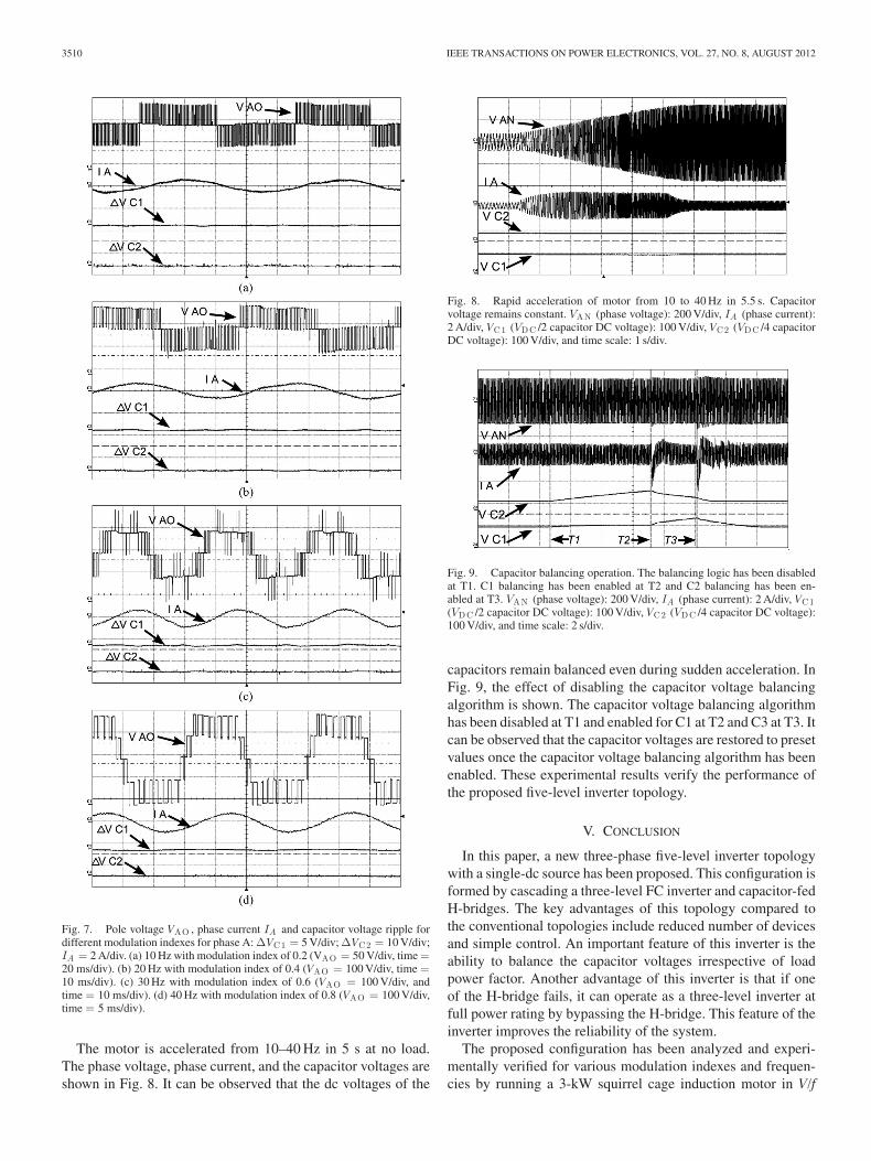
The motor is run at modulation indexes (VSV /VDC ) of 0.2, 0.4,0.6, and 0.8 at frequencies of 10, 20, 30, and 40 Hz, respectively,at no load. The phase voltage waveform along with the phasecurrent and the voltage ripple of the capacitors C1 and C2 forfrequencies of 10, 20, 30, and 40 Hz are shown in Fig. 6(a)–(d),respectively. The pole voltage waveform along with the phasecurrent at no load operation and the voltage ripple of capacitors
Fig. 6. Phase voltage VAN , phase current IA and capacitor voltage ripple fordifferent modulation indexes for phase A: ΔVC1 = 5 V/div; ΔVC2 = 10 V/div;IA = 2 A/div. (a) 10 Hz with modulation index of 0.2 (VAN = 50 V/div, time =20 ms/div). (b) 20 Hz with modulation index of 0.4 (VAN = 100 V/div, time =10 ms/div). (c) 30 Hz with modulation index of 0.6 (VAN = 100 V/div,time = 10 ms/div). (d) 40 Hz with modulation index of 0.8 (VAN = 100 V/div,time = 5 ms/div).
C1 and C2 at frequencies of 10, 20, 30, and 40 Hz are shown inFig. 7(a)–(d), respectively. The capacitor voltage ripple is lessthan 2.5 V for both C1 and C2. This validates the capacitorvoltage balancing algorithm.
3510 IEEE TRANSACTIONS ON POWER ELECTRONICS, VOL. 27, NO. 8, AUGUST 2012
Fig. 7. Pole voltage VAO , phase current IA and capacitor voltage ripple fordifferent modulation indexes for phase A: ΔVC1 = 5 V/div; ΔVC2 = 10 V/div;IA = 2 A/div. (a) 10 Hz with modulation index of 0.2 (VAO = 50 V/div, time =20 ms/div). (b) 20 Hz with modulation index of 0.4 (VAO = 100 V/div, time =10 ms/div). (c) 30 Hz with modulation index of 0.6 (VAO = 100 V/div, andtime = 10 ms/div). (d) 40 Hz with modulation index of 0.8 (VAO = 100 V/div,time = 5 ms/div).
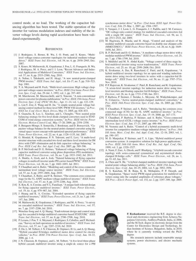
The motor is accelerated from 10–40 Hz in 5 s at no load.The phase voltage, phase current, and the capacitor voltages areshown in Fig. 8. It can be observed that the dc voltages of the
Fig. 8. Rapid acceleration of motor from 10 to 40 Hz in 5.5 s. Capacitorvoltage remains constant. VAN (phase voltage): 200 V/div, IA (phase current):2 A/div, VC1 (VDC /2 capacitor DC voltage): 100 V/div, VC2 (VDC /4 capacitorDC voltage): 100 V/div, and time scale: 1 s/div.
Fig. 9. Capacitor balancing operation. The balancing logic has been disabledat T1. C1 balancing has been enabled at T2 and C2 balancing has been en-abled at T3. VAN (phase voltage): 200 V/div, IA (phase current): 2 A/div, VC1(VDC /2 capacitor DC voltage): 100 V/div, VC2 (VDC /4 capacitor DC voltage):100 V/div, and time scale: 2 s/div.
capacitors remain balanced even during sudden acceleration. InFig. 9, the effect of disabling the capacitor voltage balancingalgorithm is shown. The capacitor voltage balancing algorithmhas been disabled at T1 and enabled for C1 at T2 and C3 at T3. Itcan be observed that the capacitor voltages are restored to presetvalues once the capacitor voltage balancing algorithm has beenenabled. These experimental results verify the performance ofthe proposed five-level inverter topology.
V. CONCLUSION
In this paper, a new three-phase five-level inverter topologywith a single-dc source has been proposed. This configuration isformed by cascading a three-level FC inverter and capacitor-fedH-bridges. The key advantages of this topology compared tothe conventional topologies include reduced number of devicesand simple control. An important feature of this inverter is theability to balance the capacitor voltages irrespective of loadpower factor. Another advantage of this inverter is that if oneof the H-bridge fails, it can operate as a three-level inverter atfull power rating by bypassing the H-bridge. This feature of theinverter improves the reliability of the system.
The proposed configuration has been analyzed and experi-mentally verified for various modulation indexes and frequen-cies by running a 3-kW squirrel cage induction motor in V/f
ROSHANKUMAR et al.: FIVE-LEVEL INVERTER TOPOLOGY WITH SINGLE-DC SUPPLY 3511
control mode, at no load. The working of the capacitor bal-ancing algorithm has been tested. The stable operation of theinverter for various modulation indexes and stability of the in-verter voltage levels during rapid acceleration have been vali-dated experimentally.
REFERENCES
[1] J. Rodriguez, S. Bernet, B. Wu, J. O. Pontt, and S. Kouro, “Multi-level voltage-source-converter topologies for industrial medium-voltagedrives,” IEEE Trans. Ind. Electron., vol. 54, no. 6, pp. 2930–2945, Dec.2007.
[2] S. Kouro, M. Malinowski, K. Gopakumar, J. Pou, L. G. Franquelo, B. Wu,J. Rodriguez, M. A. Perez, and J. I. Leon, “Recent Advances and Indus-trial Applications of Multilevel Converters,” IEEE Trans. Ind. Electron.,vol. 57, no. 8, pp. 2553–2580, Aug. 2010.
[3] A. Nabae, I. Takahashi, and H. Akagi, “A new neutral-point-clampedPWM inverter,” IEEE Trans. Ind. Appl., vol. IA-17, no. 5, pp. 518–523,Sep. 1981.
[4] T. A. Meynard and H. Foch, “Multi-level conversion: High voltage chop-pers and voltage-source inverters,” in Proc. IEEE 23rd Annu. Power Elec-tron. Spec. Conf., Jun. 29–Jul. 3, 1992, vol. 1, pp. 397–403.
[5] M. Marchesoni, M. Mazzucchelli, and S. Tenconi, “A non-conventionalpower converter for plasma stabilization,” in Proc. IEEE 19th Annu. PowerElectron. Spec. Conf. (PESC’88) Rec., Apr. 11–14, vol. 1, pp. 122–129.
[6] L. Lin;Y. Zou; Z. Wang and H. Jin, “A simple neutral-point voltage bal-ancing control method for three-level NPC PWM VSI inverters,” in Proc.IEEE Int. Conf. Electr. Mach. Drives, May 15, 2005, pp. 828–833.
[7] S. Guanchu, K. Lee, L. Xinchun, and L. Chongbo, “New neutral pointbalancing strategy for five-level diode clamped converters used in STAT-COM of wind energy conversion systems,” in Proc. IEEE 6th Int. PowerElectron. Motion Control Conf., May 17–20, 2009, pp. 2354–2358.
[8] S. Busquets-Monge, S. Somavilla, J. Bordonau, and D. Boroyevich, “Ca-pacitor voltage balance for the neutral-point-clamped converter using thevirtual space vector concept with optimized spectral performance,” IEEETrans. Power Electron., vol. 22, no. 4, pp. 1128–1135, Jul. 2007.
[9] G. Mondal, K. Gopakumar, P. N. Tekwani, and E. Levi, “A multi-levelinverter structure with cascaded two-level and three-level inverters for IMdrive with CMV elimination and dc-link capacitor voltage balancing,” inProc. IEEE Conf. Rec. Ind. Appl. Conf., Oct. 2007, pp. 589–596.
[10] B. P. McGrath and D. G. Holmes, “Enhanced voltage balancing of flyingcapacitor multilevel converter using phase disposition (PD) modulation,”IEEE Trans. Power Electron., vol. 26, no. 7, pp. 1933–1942, Jul. 2011.
[11] A. Shukla, A. Gosh, and A. Josh, “Natural balancing of flying capacitorvoltages in multicell inverter under PD carrier-based PWM,” IEEE Trans.Power Electron., vol. 26, no. 7, pp. 1682–1693, Jul. 2011.
[12] T. Chaudhari and A. Rufer, “Modeling and control of the cross-connectedinermediate level voltage source inverter,” IEEE Trans. Ind. Electron.,vol. 57, no. 8, pp. 2597–2604, Aug. 2010.
[13] T. Chaudhari, A. Rufer, and P. K. Steimer, “The common cross connectedstage for the 5 L ANPC medium voltage multilevel inverter,” IEEE Trans.Ind. Electron., vol. 57, no. 8, pp. 2279–2286, Aug. 2010.
[14] X. Kou, K. A. Corzine, and Y. L. Familiant, “A unique fault-tolerant designfor flying capacitor multilevel inverter,” IEEE Trans. Power Electron.,vol. 19, no. 4, pp. 979–987, Jul. 2004.
[15] J. Huang and K. A. Corzine, “Extended operation of flying capacitormultilevel inverters,” IEEE Trans. Power Electron., vol. 21, no. 1, pp. 140–147, Jan. 2006.
[16] M. Malinowski, K. Gopakumar, J. Rodriguez, and M. A. Perez, “A surveyon cascaded multilevel inverters,” IEEE Trans. Ind. Electron., vol. 57,no. 7, pp. 2197–2206, Jul. 2010.
[17] Wenchao Song and A. Q. Huang, “Fault-tolerant design and control strat-egy for cascaded h-bridge multilevel converter-based STATCOM,” IEEETrans. Ind. Electron., vol. 57, no. 8, pp. 2700–2708, Aug. 2010.
[18] P. Lezana, J. Pou, T. A. Meynard, J. Rodriguez, S. Ceballos, and F. Richard-eau, “Survey on fault operation on multilevel inverters,” IEEE Trans. Ind.Electron., vol. 57, no. 7, pp. 2207–2218, Jul. 2010.
[19] Z. Du, L. M. Tolbert, J. N. Chiasson, B. Ozpineci, H. Li, and A. Q. Huang,“Hybrid cascaded H-bridges multilevel motor drive control for electricvehicles,” in Proc. IEEE 37th Power Electron. Spec. Conf., Jun. 18–22,2006, pp. 1–6.
[20] J. N. Chiasson, B. Ozpineci, and L. M. Tolbert, “A five-level three-phasehybrid cascade multilevel inverter using a single-dc source for a PM
synchronous motor drive,” in Proc. 22nd Annu. IEEE Appl. Power Elec-tron. Conf., Feb. 25–Mar. 1, 2007, pp. 1504–1507.
[21] S. Vazquez, J. I. Leon, L. G. Franquelo, J. J. Padilla, and J. M. Carrasco,“DC-voltage-ratio control strategy for multilevel cascaded converters fedwith a single DC source,” IEEE Trans. Ind. Electron., vol. 56, no. 2,pp. 2513–2521, Jul. 2009.
[22] M. Hagiwara, R. Maeda, and H. Akagi, “Control and analysis of themodular multilevel cascade converter based on double-star chopper-cells(MMCCDSCC),” IEEE Trans. Power Electron., vol. 26, no. 6, pp. 1649–1658, Jul. 2011.
[23] B. P. McGrath and D. G. Holmes, “A medium-voltage motor drive with amodular multilevel PWM inverter,” IEEE Trans. Power Electron., vol. 25,no. 7, pp. 1786–1799, Jul. 2010.
[24] S. Mekhilef and M. N. Abdul Kadir, “Voltage control of three-stage hy-brid multilevel inverter using vector tranformation,” IEEE Trans. PowerElectron., vol. 25, no. 10, pp. 2599–2606, Oct. 2010.
[25] K. Sivakumar, A. Das, R. Ramchand, C. Patel, and K. Gopakumar, “Ahybrid multilevel inverter topology for an open-end winding induction-motor drive using two-level inverters in series with a capacitor-fed H-bridge cell,” IEEE Trans. Ind. Electron., vol. 56, no. 11, pp. 3707–3714,Nov. 2010.
[26] P. P. Rajeevan, K. Sivakumar, C. Patel, R. Ramchand, and K. Gopakumar,“A seven-level inverter topology for induction motor drive using two-level inverters and floating capacitor fed H-bridges,” IEEE Trans. PowerElectron., vol. 26, no. 6, pp. 1733–1740, Jun. 2011.
[27] P. Barbosa, P. Steimer, J. Steinke, L. Meysenc, M. Winkelnkemper, andN. Celanovic, “Active neutral-point-clamped multilevel converters,” inProc. IEEE 36th Power Electron. Spec. Conf., Jun. 16, 2005, pp. 2296–2301.
[28] T. Chaudhuri, P. Steimer, and A. Rufer, “Introducing the common crossconnected stage (C3S) for the 5L ANPC multilevel inverter,” in Proc.IEEE Power Electron. Spec. Conf., Jun. 15–19, 2008, pp. 167–173.
[29] T. Chaudhuri, P. Barbosa, P. Steimer, and A. Rufer, “Cross-connectedintermediate level (CCIL) voltage source inverter,” in Proc. IEEE PowerElectron. Spec. Conf., Jun. 17–21, 2007, pp. 490–496.
[30] M. Veenstra and A. Rufer, “Control of a hybrid asymmetric multi-levelinverter for competitive medium-voltage industrial drives,” in Proc. 38thIAS Annu. Meet.. Conf. Rec. Ind. Appl. Conf., Oct. 12–16, 2003, vol. 1,pp. 190–197.
[31] M. D. Manjrekar, P. Steimer, and T. A. Lipo, “Hybrid multilevel powerconversion system: A competitive solution for high power applications,”in Proc. IEEE 34th IAS Annu. Meet. Conf. Rec. Ind. Appl. Conf., Oct.1999, vol. 3, pp. 1520–1527.
[32] A. Nami, F. Zare, A. Ghosh, and F. Blaabjerg, “A hybrid cascade convertertopology with series-connected symmetrical and asymmetrical diode-clamped H-bridge cells,” IEEE Trans. Power Electron., vol. 26, no. 1,pp. 51–65, Jan. 2011.
[33] A. Chen and X. He, “A hybrid clamped multilevel inverter topology withneutral point voltage balancing ability,” in Proc. IEEE 35th Annu. PowerElectron. Spec. Conf., Jun. 20–25, 2004, vol. 5, pp. 3952–3956.
[34] R. S. Kanchan, M. R. Baiju, K. K. Mohapatra, P. P. Ouseph, andK. Gopakumar, “Space vector PWM signal generation for multilevel in-verters using only the sampled amplitudes of reference phase voltages,”IEE Proc.—Electr. Power Appl., vol. 152, no. 2, pp. 3297–309, Apr. 2005.
P. Roshankumar received the B.E. degree in elec-trical and electronics engineering from Acharya Na-garjuna University, Andhrya Pradesh, India, in 2006,and the M.Tech. degree in electronic design from theCentre for Electronics Design and Technology, In-dian Institute of Science, Bangalore, India, in 2010,where he is currently working toward the Ph.D.degree
His research interests include renewable energysystems, power electronics, and electro mechanicsystems.

3512 IEEE TRANSACTIONS ON POWER ELECTRONICS, VOL. 27, NO. 8, AUGUST 2012
P. P. Rajeevan received the B.Tech. degree in elec-trical engineering from the University of Calicut,Kerala, India, and the M.E. degree in power elec-tronics from Bangalore University, Bangalore, India.He is currently working toward the Ph.D. degree atthe Centre for Electronics Design and Technology,Indian Institute of Science, Bangalore.
His research interests include multilevel powerconverters, drives, pulse-width modulation tech-niques, and power quality.
K. Mathew received the B.E. degree in electron-ics and communication engineering from KurunjiVenkatramana Gowda Engineering College, Manga-lore, India in 1994, and the M.Tech. degree in elec-tronic design from the Centre for Electronics De-sign and Technology, Indian Institute of Science,Bangalore, India, in 2006, where he is currently work-ing toward the Ph.D. degree.
He is a Faculty Member in the Department ofElectronics Engineering, Mar Athanasius College ofEngineering, Kothamangalam, India. His research in-
terests include embedded systems, power electronics, and electro mechanicsystems.
K. Gopakumar (M’94–SM’96–F’11) received theB.E., M.Sc. (Engg.), and Ph.D. degrees from the In-dian Institute of Science, Bangalore, India, in 1980,1984, and 1994, respectively.
He was with the Indian Space Research Organi-zation, Bangalore, India from 1984 to 1987. He cur-rently holds the position of Chairman and Professorat the Center for Electronics Design and Technology,Indian Institute of Science. His research interests in-clude pulse-width modulation converters and highpower drives.
Dr. Gopakumar is a Fellow of Institution of Electrical and Telecommunica-tion Engineers, India and Indian National Academy of Engineers. He is currentlyan Associate Editor of the IEEE TRANSACTION ON INDUSTRIAL ELECTRONICS.
Jose I. Leon (S’04–M’07) was born in Cadiz, Spain,in 1976. He received the B.S., M.S., and Ph.D. de-grees in telecommunications engineering from theUniversity of Seville (US), Seville, Spain, in 1999,2001 and 2006, respectively.
He is currently an Associate Professor with the De-partment of Electronic Engineering, US. His researchinterests include electronic power systems, modula-tion and control of power converters, and industrialdrives.
Dr. Leon recieved the 2008 Best Paper Award ofthe IEEE Industrial Electronics Magazine as the coauthor.
Leopoldo G. Franquelo (M’84–SM’96–F’05), re-ceived the M.Sc. and Ph.D. degrees in electrical engi-neering from the University of Seville, Seville, Spain,in 1977 and 1980, respectively.
He was the Head of the Electronics EngineeringDepartment (1998–2005). He is currently a Full pro-fessor and the Head of the Power Electronics Groupwith the University of Seville. From 2002 to 2003,he was the Vice President of the Industrial Electron-ics Society (IES) Spanish Chapter and a Member atlarge of the IES Administrative Committee. He was
the Vice President for conferences (2004–2007), in which he has also been aDistinguished Lecturer since 2006. He is the holder of ten patents and partici-pated in 96 R&D projects. He has been the president of IES (2010–2011). He isthe author of more than 60 publications in international journals and 180 papersin international conference proceedings. His current research interests includemodulation techniques for multilevel inverters and its application to power elec-tronic systems for renewable energy systems.
Dr. Franquelo has been an Associate Editor of the IEEE TRANSACTIONS ON
INDUSTRIAL ELECTRONICS since 2007.