Embed Size (px)
Citation preview

A FIRST PRINCIPLES STUDY OF
DEFECTS IN SEMICONDUCTORS
Submitted by Jonathan Paul Goss to the University of Exeter as a thesis for the
degree of Doctor of Philosophy in Physics in the Faculty of Science, January 1997.
This thesis is available for the Library use on the understanding that it is copyright
material and that no quotation from the thesis may be published without proper
acknowledgement.
Declaration: I certify that all material in this thesis which is not my own work has
been identified and that no material is included for which a degree has previously
been conferred upon me,
1

Abstract
This thesis reports the results of ab initio calculations performed using AIMPRO,
a local-spin-density-functional, real-space cluster code. The clusters are typically
70-200 atoms in size and are all hydrogen terminated to passivate the surface dan-
gling bonds. Using this approach a large number of defects have been examined in
diamond, silicon, and gallium arsenide.
Defects in diamond are of great interest from an optical point of view, and the
properties of a range of vacancy-impurity complexes are examined in detail. Syn-
thetic diamonds grown using transition metal catalysts exhibit pronounced optical
features which have been correlated with nickel. Reported here are the structures
of Ni point defects and Ni-impurity complexes.
Transition metals are also important impurities in Si due to the device implica-
tions. Substitutional Ni undergoes a subtle Jahn-Teller distortion in the negative
charge state, which is reproduced in these calculations. Ni-H2 complexes are also
reported.
Finally, the use of C as an acceptor in GaAs has many advantages such as
its low diffusivity and samples can be doped with high concentrations. However,
C readily complexes with H to form electrically inactive centres. Reported here
are the results of a study of the anharmonicity of the C-H stretch mode and the
structures of di-carbon-hydrogen complexes that exhibit strongly polarised local
vibrational modes.
2

Acknowledgements
I would like to thank the Physics Department and EPSRC for providing the neces-
sary environment and funds for the duration of my PhD in Exeter.
I would very much like to acknowledge the following people for their contribu-
tions to my PhD.
First of all Bob Jones for his stalwart supervision, tuition and sense of humour.
Also the AIMPRO-family: Malc, Pat, Chris (for whom I gratefully acknowledge top
tips on EPR and groovy diagram - Fig. 3.2, LHS), and Sven for their diverse forms of
role model. SpudmanTM 1, The-P***-Artist-Formally-Known-As-Lard and Stevie-
B have made the contents of this thesis slightly less mystifying to me, as well as the
consumption of C2H5OH increase exponentially. And there are all the others that
have been involved somewhere down the line: Paul Sitch, Bernd, Vitor, Deepak,
Joci, Antonio, Ben Hur, Gerd, Steve Maynard...
More generally, I have found my time at Exeter both more enlightening and
more hazy in part due to my non-AIMPRO, Exeter-family: Big-Nose, Paul Rawlins,
Will, Susie, GP, JMR, Mauro, ‘Topher Townsley, Sai, Mike, Jonathan Warren, Tim,
Elaine, Paul Wright, Huseyin, Mehmet, and too many others to mention.
I would like to thank my (real-life?) family: Prim, Sid, Dave and Jackie, for
their support when I gave up a life of leisure in the NHS for three years hard labour
in the salt mines.
Finally my (most heart-felt) thanks must go to long suffering Sarah for her
constant support and encouragement since time began.
1Serum sum, ergo sum
3

Contents
Contents 4
List of Publications 8
List of Tables 10
List of Figures 13
1 Introduction 19
2 Theory 23
2.1 Introduction . . . . . . . . . . . . . . . . . . . . . . . . . . . . . . . 23
2.2 The problem posed . . . . . . . . . . . . . . . . . . . . . . . . . . . 24
2.3 The Born-Oppenheimer approximation . . . . . . . . . . . . . . . . 25
2.4 Hartree-Fock Theory . . . . . . . . . . . . . . . . . . . . . . . . . . 25
2.5 Parameterised Hartree-Fock methods . . . . . . . . . . . . . . . . . 28
2.5.1 Complete neglect of differential overlap . . . . . . . . . . . . 29
2.5.2 CNDO/1 . . . . . . . . . . . . . . . . . . . . . . . . . . . . . 31
2.5.3 CNDO/2 . . . . . . . . . . . . . . . . . . . . . . . . . . . . . 31
2.5.4 Intermediate neglect of differential overlap . . . . . . . . . . 32
2.5.5 Neglect of diatomic differential overlap . . . . . . . . . . . . 32
2.5.6 Summary . . . . . . . . . . . . . . . . . . . . . . . . . . . . 32
2.6 Hartree-Fock theory of the homogeneous electron gas . . . . . . . . 33
2.7 Correlation . . . . . . . . . . . . . . . . . . . . . . . . . . . . . . . 33
2.8 Density functional theory . . . . . . . . . . . . . . . . . . . . . . . . 34
2.9 The local density approximation . . . . . . . . . . . . . . . . . . . . 36
2.10 Determination of the Kohn-Sham orbitals . . . . . . . . . . . . . . 37
2.11 Pseudopotentials . . . . . . . . . . . . . . . . . . . . . . . . . . . . 37
2.12 AIMPRO methodology . . . . . . . . . . . . . . . . . . . . . . . . . 40
2.12.1 Evaluation of the Hartree energy . . . . . . . . . . . . . . . 41
2.12.2 Exchange-correlation energy . . . . . . . . . . . . . . . . . . 42
4
CONTENTS 5
2.12.3 Arrival at the eigenvalue equation . . . . . . . . . . . . . . . 44
2.13 The self-consistent cycle . . . . . . . . . . . . . . . . . . . . . . . . 45
2.13.1 The ‘Fermi temperature’ . . . . . . . . . . . . . . . . . . . . 47
2.14 Structural optimisation . . . . . . . . . . . . . . . . . . . . . . . . . 47
2.14.1 Atomic forces . . . . . . . . . . . . . . . . . . . . . . . . . . 48
2.14.2 Conjugate gradients optimisation . . . . . . . . . . . . . . . 48
2.15 Vibrational modes . . . . . . . . . . . . . . . . . . . . . . . . . . . 49
2.15.1 Musgrave-Pople valence force potentials . . . . . . . . . . . 50
2.15.2 Anharmonicity . . . . . . . . . . . . . . . . . . . . . . . . . 51
2.15.2.1 Quantifying anharmonicity . . . . . . . . . . . . . 51
2.15.2.2 Theoretical approach . . . . . . . . . . . . . . . . . 53
2.15.2.3 Electrical anharmonicity . . . . . . . . . . . . . . . 57
2.15.2.4 Theoretical evaluation of χ. . . . . . . . . . . . . . 58
2.15.3 Effective charges . . . . . . . . . . . . . . . . . . . . . . . . 59
2.16 Multiplets . . . . . . . . . . . . . . . . . . . . . . . . . . . . . . . . 60
2.17 Electronic transitions . . . . . . . . . . . . . . . . . . . . . . . . . . 60
2.17.1 Transition states . . . . . . . . . . . . . . . . . . . . . . . . 61
2.17.2 Radiative lifetimes . . . . . . . . . . . . . . . . . . . . . . . 61
2.18 Clusters . . . . . . . . . . . . . . . . . . . . . . . . . . . . . . . . . 61
2.19 Summary . . . . . . . . . . . . . . . . . . . . . . . . . . . . . . . . 64
3 Experimental techniques 65
3.1 Introduction . . . . . . . . . . . . . . . . . . . . . . . . . . . . . . . 65
3.2 Localised vibrational mode spectroscopy . . . . . . . . . . . . . . . 66
3.2.1 Infra-red absorption . . . . . . . . . . . . . . . . . . . . . . 66
3.2.2 Raman scattering . . . . . . . . . . . . . . . . . . . . . . . . 70
3.2.3 Summary . . . . . . . . . . . . . . . . . . . . . . . . . . . . 72
3.3 Electron paramagnetic resonance . . . . . . . . . . . . . . . . . . . 73
3.3.1 Dipolar magnetic moment . . . . . . . . . . . . . . . . . . . 73
3.3.2 Absorption and derivative outputs . . . . . . . . . . . . . . . 74
3.3.3 Nuclear Zeeman effect . . . . . . . . . . . . . . . . . . . . . 74
3.3.4 The hyperfine interaction . . . . . . . . . . . . . . . . . . . . 75
3.3.5 Spin orbit coupling . . . . . . . . . . . . . . . . . . . . . . . 76
3.3.6 High spin centres . . . . . . . . . . . . . . . . . . . . . . . . 76
3.3.7 Low symmetry defects . . . . . . . . . . . . . . . . . . . . . 76
3.3.8 Optical detection of magnetic resonance . . . . . . . . . . . 77
3.3.9 Summary . . . . . . . . . . . . . . . . . . . . . . . . . . . . 77
3.4 Photoluminescence . . . . . . . . . . . . . . . . . . . . . . . . . . . 78

CONTENTS 6
3.5 Deep level transient spectroscopy . . . . . . . . . . . . . . . . . . . 82
4 Vacancy-X complexes in diamond 87
4.1 Introduction . . . . . . . . . . . . . . . . . . . . . . . . . . . . . . . 87
4.2 The vacancy . . . . . . . . . . . . . . . . . . . . . . . . . . . . . . . 89
4.3 Vacancy-nitrogen complexes . . . . . . . . . . . . . . . . . . . . . . 90
4.3.1 Cluster and basis. . . . . . . . . . . . . . . . . . . . . . . . . 91
4.3.2 The vacancy bordered by a N atom . . . . . . . . . . . . . . 92
4.3.3 The vacancy bordered by three N atoms . . . . . . . . . . . 94
4.3.4 Conclusions . . . . . . . . . . . . . . . . . . . . . . . . . . . 96
4.4 The vacancy-silicon complex . . . . . . . . . . . . . . . . . . . . . . 96
4.4.1 Cluster and basis. . . . . . . . . . . . . . . . . . . . . . . . . 97
4.4.2 Results . . . . . . . . . . . . . . . . . . . . . . . . . . . . . . 97
4.5 The vacancy-phosphorus complex. . . . . . . . . . . . . . . . . . . . 99
4.5.1 Introduction . . . . . . . . . . . . . . . . . . . . . . . . . . . 99
4.5.2 Cluster and basis. . . . . . . . . . . . . . . . . . . . . . . . . 100
4.5.3 Results . . . . . . . . . . . . . . . . . . . . . . . . . . . . . . 100
4.5.4 Summary . . . . . . . . . . . . . . . . . . . . . . . . . . . . 103
4.6 Vacancy-hydrogen complexes . . . . . . . . . . . . . . . . . . . . . . 103
4.6.1 Introduction . . . . . . . . . . . . . . . . . . . . . . . . . . . 103
4.6.2 Cluster and basis . . . . . . . . . . . . . . . . . . . . . . . . 104
4.6.3 VH . . . . . . . . . . . . . . . . . . . . . . . . . . . . . . . . 105
4.6.4 VH2 . . . . . . . . . . . . . . . . . . . . . . . . . . . . . . . 107
4.6.5 VH3 and VH4 . . . . . . . . . . . . . . . . . . . . . . . . . . 109
4.6.6 Stabilities of VHn . . . . . . . . . . . . . . . . . . . . . . . . 110
4.6.7 V2H . . . . . . . . . . . . . . . . . . . . . . . . . . . . . . . 111
4.6.8 Conclusion . . . . . . . . . . . . . . . . . . . . . . . . . . . . 111
4.7 Summary . . . . . . . . . . . . . . . . . . . . . . . . . . . . . . . . 112
5 Nickel and Ni-X centres in diamond and Si 114
5.1 Nickel in diamond . . . . . . . . . . . . . . . . . . . . . . . . . . . . 114
5.1.1 Introduction . . . . . . . . . . . . . . . . . . . . . . . . . . . 114
5.1.2 Experimental background . . . . . . . . . . . . . . . . . . . 115
5.1.2.1 Magnetic centres . . . . . . . . . . . . . . . . . . . 115
5.1.2.2 Optical centres . . . . . . . . . . . . . . . . . . . . 116
5.1.3 Electronic structure of Ni in group IV semiconductors . . . . 117
5.1.4 Previous calculations . . . . . . . . . . . . . . . . . . . . . . 119
5.1.5 AIMPRO calculations . . . . . . . . . . . . . . . . . . . . . 120
5.1.5.1 Cluster and basis . . . . . . . . . . . . . . . . . . . 120

CONTENTS 7
5.1.5.2 Nickel carbonyl . . . . . . . . . . . . . . . . . . . . 121
5.1.5.3 Interstitial Ni+ . . . . . . . . . . . . . . . . . . . . 121
5.1.5.4 The Ni+i -B−s complex . . . . . . . . . . . . . . . . . 123
5.1.5.5 Substitutional Ni− . . . . . . . . . . . . . . . . . . 124
5.1.5.6 The Ni−s -N+s complex . . . . . . . . . . . . . . . . . 126
5.1.5.7 Substitutional Ni+ . . . . . . . . . . . . . . . . . . 127
5.1.5.8 The Ni+s -B−s complex . . . . . . . . . . . . . . . . . 128
5.1.5.9 Radiative lifetimes . . . . . . . . . . . . . . . . . . 128
5.1.6 Conclusions . . . . . . . . . . . . . . . . . . . . . . . . . . . 130
5.2 Nickel and nickel-hydrogen complexes in Si . . . . . . . . . . . . . . 133
5.2.1 Introduction . . . . . . . . . . . . . . . . . . . . . . . . . . . 133
5.2.2 Cluster and basis . . . . . . . . . . . . . . . . . . . . . . . . 134
5.2.3 Results . . . . . . . . . . . . . . . . . . . . . . . . . . . . . . 135
5.2.4 Conclusions . . . . . . . . . . . . . . . . . . . . . . . . . . . 139
6 Carbon-Hydrogen complexes in GaAs. 140
6.1 Introduction . . . . . . . . . . . . . . . . . . . . . . . . . . . . . . . 140
6.2 Anharmonic theory of the CAs-H complex. . . . . . . . . . . . . . . 140
6.2.1 Introduction. . . . . . . . . . . . . . . . . . . . . . . . . . . 140
6.2.2 Experimental background & previous theoretical studies. . . 141
6.2.3 Clusters and basis. . . . . . . . . . . . . . . . . . . . . . . . 143
6.2.4 Prussic acid molecule: HCN . . . . . . . . . . . . . . . . . . 143
6.2.5 The CAs-H stretch mode . . . . . . . . . . . . . . . . . . . . 146
6.2.6 The intensity of the overtone . . . . . . . . . . . . . . . . . . 150
6.2.7 Conclusions . . . . . . . . . . . . . . . . . . . . . . . . . . . 151
6.3 Theory of hydrogenated CAs-dimers. . . . . . . . . . . . . . . . . . 152
6.3.1 Clusters and basis. . . . . . . . . . . . . . . . . . . . . . . . 155
6.3.2 Results. . . . . . . . . . . . . . . . . . . . . . . . . . . . . . 155
6.3.2.1 The (CAs)2-H complex. . . . . . . . . . . . . . . . 156
6.3.2.2 The (CAs)2-H2 complex. . . . . . . . . . . . . . . . 158
6.3.3 Conclusions. . . . . . . . . . . . . . . . . . . . . . . . . . . . 160
7 Conclusions 161
A Character tables 165
B Jahn-Teller distortions 166
References 168

List of Published Papers
Listed in reverse chronological order:
1. ‘First principles theory of impurity-vacancy complexes in diamond’, J. P. Goss,
R. Jones, S. J. Breuer, P. R. Briddon, and S. Oberg, proceedings of the 23rd
International Conference on the Physics of Semiconductors, 1996, pp. 2577-
80, (World Scientific, Singapore, New Jersey, London, Hong Kong), ed. M.
Scheffler and R. Zimmermann.
2. ‘Is hydrogen anti bonded in hydrogenated GaAs:Mg?’ R. Bouanani-Rabi, B.
Pajot, C. P. Ewels, S. Oberg, J. Goss, R. Jones, Y. Nissim, B. Theys, and
C. Blaauw. To be published in the proceedings of SLCS96, ’Shallow Level
Centers in Semiconductors’, Amsterdam, 1996.
3. ‘The twelve line 1.682 eV luminescence center in diamond and the vacancy-
silicon complex’, J. Goss, R. Jones, S. J. Breuer, P. R. Briddon, and S. Oberg,
Phys. Rev. Lett. 77, 3041 (1996).
4. ‘Limitations to n-type doping in diamond: the phosphorus-vacancy complex’,
R. Jones, J. E. Lowther, and J. Goss, Appl. Phys. Lett. 69, 2489 (1996).
5. ‘The nitrogen-pair oxygen defect in silicon’, F. Berg Rasmussen, S. Oberg, R.
Jones, C. Ewels, J. Goss, J. Miro, and P. Deak, NATO ARW ’Early Stages
of Oxygen Precipitation in Silicon’, ed. R. Jones, Kluwer Academic Press, p.
319.
6. ‘Local modes of the H∗2 dimer in germanium’, M. Budde, B. Bech Neilsen, R.
Jones, J. Goss, and S. Oberg, Phys. Rev. B 54, 5485 (1996).
7. ‘The nitrogen-pair oxygen defect in Silicon’, F. Berg Rasmussen, S. Oberg, R.
Jones, C. Ewels, J. Goss, J. Miro, and P. Deak, Mat. Sci. Eng. B, 36, 91-95
(1996).
8. ‘Theory of nickel and nickel-hydrogen complexes in silicon’, R. Jones , S.
Oberg, J. Goss, P. R. Briddon, and A. Resende, Phys. Rev. Lett 75, 2734
(1995).
9. ‘Ni complexes in diamond’, J. Goss, A. Resende, R. Jones, S. Oberg, and
P. R. Briddon, Mat. Sci. Forum Vol. 196-201, pp 67-72 (1995), Trans Tech
Publications, Switzerland.
8

CONTENTS 9
10. ‘The NNO defect in Silicon’, F. Berg Rasmussen, S. Oberg, R. Jones, C.
Ewels, J. Goss, J. Miro, and P. Deak, Mat. Sci. Forum Vol. 196-201, pp
791-796 (1995), Trans Tech Publications, Switzerland.
11. ‘The H∗2 defect in crystalline germanium’, M. Budde, B. Bech Neilsen, R.
Jones, S. Oberg, and J. Goss, Mat. Sci. Forum Vol. 196-201, pp 879-884
(1995), Trans Tech Publications, Switzerland.
12. ‘Theory of the NiH2 complex in Si and the CuH2 complex in GaAs’, R. Jones,
J. Goss, S. Oberg, P. R. Briddon, and A. Resende, Mat. Sci. Forum Vol. 196-
201, pp 921-926 (1995), Trans Tech Publications, Switzerland.
13. ‘H interacting with intrinsic defects in Si’, B. Bech Neilsen, L. Hoffmann, M.
Budde, R. Jones, J. Goss, and S. Oberg, Mat. Sci. Forum Vol. 196-201, pp
933-938 (1995), Trans Tech Publications, Switzerland.
14. ‘The nitrogen-pair oxygen defect in silicon’, F. Berg Rasmussen, S. Oberg, R.
Jones, C. Ewels, J. Goss, J. Miro, and P. Deak, E-MRS, Strasbourg, (1995).
15. ‘H passivated defects in InP’, C. P. Ewels, S. Oberg, P. R. Briddon, J. Goss,
R. Jones, S. Breuer, R. Darwich, and B. Pajot, Solid State Communications
93 5, pp.459-460 (1995). Paper for SLCS94, ‘Shallow Level Centers in Semi-
conductors’, Berkeley, 1994.
16. ‘The Hydrogen complexes in GaAs and InP doped with Magnesium’, R.
Rahbi, B. Pajot, C. Ewels, S. Oberg, J. Goss, R. Jones, Y. Nissim, B. Theys,
and C. Blaauw. Solid State Communications 93 5, pp.462 (1995). Paper for
SLCS94, ‘Shallow Level Centers in Semiconductors’, Berkeley, 1994.
17. ‘Theoretical and Isotopic Infrared Absorption Investigations of Nitrogen-Oxy-
gen Defects in Silicon’, R. Jones, C. Ewels, J. Goss, J. Miro, P. Deak, S. Oberg,
and F. Berg Rasmussen, Semiconductor Science and Technology 9, 2145-48,
(1994).
18. ‘Ab Initio Calculations of Anharmonicity of the C-H stretch mode in HCN
and GaAs’, R. Jones, J. Goss, C. Ewels, and S. Oberg, Phys. Rev. B 50,
8378-88, (1994).

List of Tables
2.1 Parameterisation of the exchange-correlation energy in Ref. [27]. . . 34
2.2 Parameterisation of the exchange-correlation used in AIMPRO. . . 35
4.1 A summary of the classification of diamonds. . . . . . . . . . . . . . 88
4.2 The atomic basis used for the calculations in Sec. 4.3. . . . . . . . . 91
4.3 The atomic basis used for the calculations in Sec. 4.4. . . . . . . . . 97
4.4 The atomic basis used for the calculations in Sec. 4.5. . . . . . . . . 100
4.5 The atomic basis used for the calculations in Sec. 4.3. . . . . . . . . 105
4.6 The H/D stretch modes (cm−1) associated with four charge/spin
states of VH. . . . . . . . . . . . . . . . . . . . . . . . . . . . . . . 107
4.7 The H/D stretch modes (cm−1) associated with three charge states
of VH2. . . . . . . . . . . . . . . . . . . . . . . . . . . . . . . . . . 108
4.8 The H/D stretch modes (cm−1) associated with the neutral VH3,
VH4, and V2H complexes. . . . . . . . . . . . . . . . . . . . . . . . 110
4.9 The total energies of the clusters containing VHn and VHn−1-Hb−c
systems for n=1,2,3,4. Note that in all cases, H prefers to be located
within the vacancy. . . . . . . . . . . . . . . . . . . . . . . . . . . . 110
4.10 A table of the main optical transitions expected for VHn, n = 1, 2, 3
in diamond. . . . . . . . . . . . . . . . . . . . . . . . . . . . . . . . 112
5.1 The atomic basis used for the calculations in Sec. 5.1. . . . . . . . . 121
5.2 The dipole-allowed transitions for Ni and Ni-X centres. The transi-
tions are written in terms of the absorption. All transition energies
[eV], ∆E, are found from the difference between the calculated Kohn-
Sham eigenvalues, and the dipole matrix elements squared are also
listed (P 2ij). The radiative lifetimes, τ are listed in ns unless stated
otherwise. . . . . . . . . . . . . . . . . . . . . . . . . . . . . . . . . 129
5.3 The atomic basis used for the calculations in Sec. 5.2. . . . . . . . . 134
5.4 Vibrational Modes (cm−1) for the TM-H−2 AB defect . . . . . . . . 138
6.1 The atomic basis used for the calculations in Sec. 6.2. . . . . . . . . 143
10

LIST OF TABLES 11
6.2 The calculated and experimental [191] structure (A) and vibrational
modes (cm−1) of the HCN molecule. . . . . . . . . . . . . . . . . . 143
6.3 Calculated energy double derivatives for HCN (a.u.). . . . . . . . . 144
6.4 Calculated polynomial coefficients (a.u.) for the fit to the vibronic
potential of HCN. . . . . . . . . . . . . . . . . . . . . . . . . . . . . 145
6.5 Calculated and observed anharmonic C-H frequencies (cm−1) of the
HCN molecule. . . . . . . . . . . . . . . . . . . . . . . . . . . . . . 145
6.6 Calculated double derivatives for CAs-H (a.u.). . . . . . . . . . . . 147
6.7 Calculated and observed [70, 215] LVMs (cm−1) due to CAs-H in
GaAs. . . . . . . . . . . . . . . . . . . . . . . . . . . . . . . . . . . 147
6.8 Calculated polynomial coefficients (a.u.) for the fit to the vibronic
potential of CAs-H in GaAs. . . . . . . . . . . . . . . . . . . . . . . 147
6.9 Calculated and experimental [51, 207, 208] anharmonic CAs-H fre-
quencies (cm−1) for the ab initio bond length, 1.126 A. . . . . . . . 148
6.10 Calculated and experimental [51, 207, 208] anharmonic CAs-H fre-
quencies (cm−1) for the lengthened C-H bond (1.161 A). . . . . . . 148
6.11 The atomic basis used for the calculations in Sec. 6.3. . . . . . . . . 155
6.12 The bond lengths of the relaxed (CAs)2, (CAs) − H, (CAs)2 − H and
(CAs)2 − H2. The C1-Ga and C2-Ga lengths are to the common
Ga neighbour. The ‘back’ bonds refer to the three remaining C-Ga
separations shown in Figs. 6.9 and 6.10. All lengths are in A. . . . . 156
6.13 The C-H stretch modes of the lowest energy C1-H-Ga-C2 system
(cm−1) for the various combinations of carbon and hydrogen isotopes
in the 132 and 164 atom clusters. Note, the C1-H stretch mode is
unaffected by a change in mass of C2. . . . . . . . . . . . . . . . . . 156
6.14 The projection onto the [110], [110], and [001] directions of the C-
H stretch mode of the C1h symmetry (CAs)2H complex, calculated
in the 132 atom cluster (cm−1). The C atoms are labelled 1 and 2
according to Fig. 6.9. The mode is symmetric about the C1h mirror
plane. . . . . . . . . . . . . . . . . . . . . . . . . . . . . . . . . . . 157
6.15 The C-H stretch modes for the 133 atom clusters (cm−1) and total
energies for the 133 and 165 atom clusters, Etot (eV), relative to the
(1,3) pairing for the seven configurations of the (CAs)2H2 complex.
The models are labelled according to pairing of hydrogen atoms as
described in Fig. 6.10. . . . . . . . . . . . . . . . . . . . . . . . . . 158

LIST OF TABLES 12
6.16 The C-H stretch modes of the lowest energy (CAs)2H2 model (1,3)
(Fig. 6.10) in the 133 and 165 atom clusters (cm−1). Since the two C-
H units are practically decoupled, only a subset of the permutations
of isotopes is required. The modes are not shifted significantly by
the Ga mass. . . . . . . . . . . . . . . . . . . . . . . . . . . . . . . 158
6.17 The projection onto the [110], [110], and [001] directions of the nor-
mal stretch modes of the C1 symmetry (CAs)2H2 complex (cm−1).
The C atoms are labelled 1 and 2 according to Fig. 6.10. . . . . . . 159

List of Figures
1.1 Diagram showing the 71-atom tetrahedral cluster (X35H36). . . . . . 20
2.1 Plots showing the solutions to the secular equations 2.41 where (a)
No = 30, and (b) No = 90. The displacement, x, is in a.u., and
the wavefunctions have been shifted vertically so that each is zeroed
about its energy level. . . . . . . . . . . . . . . . . . . . . . . . . . 56
2.2 A plot of the polynomial potential as plotted in Fig. 2.1 also showing
the Morse potential fit. . . . . . . . . . . . . . . . . . . . . . . . . 57
2.3 A plot of the non-linear dipole moment of the CAs − H complex in
GaAs, p(x), x in a.u. . . . . . . . . . . . . . . . . . . . . . . . . . . 58
2.4 A graph showing the dependence on cluster size of the band-gap for
diamond, Si, Ge, and GaAs. The group-IV materials clusters are
made up as follows: X35H36, X71H60, and X181H116. There are two
possible arrangements of each GaAs cluster - Ga centred and As cen-
tred. The three clusters are X19Y16H36, X31Y40H60, and X89Y92H116.
In the graph, ×’s indicate Ga centred clusters and ©’s As centred
clusters. (cf. experimental values of the band-gap: 5.5, 1.17, 0.75,
and 1.42 eV for diamond, Si, Ge, and GaAs respectively.) . . . . . . 64
3.1 The one-dimension phonon-dispersion for a material with zinc blende
like structure. . . . . . . . . . . . . . . . . . . . . . . . . . . . . . . 67
3.2 On the left is shown how the experiment is set up such that the modu-
lation is used as a reference to enhance the modulated output using a
phase sensitive detector (PSD). On the right is shown a schematic of
the absorption and absorption derivative EPR spectra. The ‘wave’
indicated by ‘(MA)’ shows the modulated absorption produced by
the modulated magnetic field, ∆B. . . . . . . . . . . . . . . . . . . 75
13

LIST OF FIGURES 14
3.3 Schematic representations of PL in the cases where (a) the transition
observed is from the first excited state to the ground state, and (b)
where, since such a transition is forbidden, a transition from the
second excited state to the ground state, as suggested for the N2/N3
optical systems in diamond [74]. . . . . . . . . . . . . . . . . . . . . 79
3.4 Schematic representations of (a) absorption and (b) PLE where tran-
sitions involving all excited states are seen. . . . . . . . . . . . . . . 80
3.5 Schematics of the conduction (EC) and valence (EV) bands bending
at the p-n or Schottky junction. Plots are shown for two reverse
biases, V1 and V2. The junction is located at x=0, and the distances
xi and λi are described in the text. . . . . . . . . . . . . . . . . . . 83
3.6 A plot of the reverse bias pulse and capacitance response. . . . . . . 84
3.7 A graph showing how the capacitance transient changes with increas-
ing temperature, T . T0 < T1 < T2 < T3 < T4. Also marked is the
time-window for which the DLTS spectrum is taken. Note, for tem-
peratures T0 and T4 there is no change in capacitance over the range
of the time-window. . . . . . . . . . . . . . . . . . . . . . . . . . . . 85
3.8 A plot showing a typical DLTS spectrum. There are three peaks
which correspond approximately to the energies of three deep traps. 86
4.1 The spin-polarised Kohn-Sham eigenvalues for the V-N complex in
diamond. Only the states in the region of the gap are plotted. Ar-
rows indicate occupation and spin, and the empty boxes show empty
states. The ‘valence band tops’ have been aligned to facilitate com-
parison. . . . . . . . . . . . . . . . . . . . . . . . . . . . . . . . . . 92
4.2 A contour plot for one of the e-level wavefunctions (au) of [V-N]−.
The plane passes through the vacancy site which is at the centre of
the plot, and also through the N and one C atom. Note that the level
is nodal at the N atom. The second e-level is qualitatively similar. . 93
4.3 The spin-polarised Kohn-Sham eigenvalues for the [V-N3]0 complex
in diamond. Shown are the 2A1 ground state, and the 2E excited
state associated with the N3 optical transition. Also shown is an2A1 excited state which is found to be the lowest in energy. This is
associated with the N2 vibronic centre. Only the states in the region
of the gap are plotted. Arrows indicate occupation and spin, and the
empty boxes show empty states. . . . . . . . . . . . . . . . . . . . . 94

LIST OF FIGURES 15
4.4 A schematic representation of the relaxed split-vacancy geometry of
the V-Si complex. The solid circles represent C atoms, the empty
circle the relaxed Si site, and the dashed circles the diamond lattice
sites. . . . . . . . . . . . . . . . . . . . . . . . . . . . . . . . . . . . 98
4.5 The spin-polarised Kohn-Sham eigenvalues for the V-Si complex in
diamond in the region of the band gap. The notation is as in Fig. 4.1,
and the ‘valence band tops’ aligned. . . . . . . . . . . . . . . . . . . 99
4.6 Kohn-Sham eigenvalues of the [P-V] complex in diamond in vicinity
of the band gap. The arrows and filled boxes denote spin polarised
and non-polarised occupied levels respectively and the empty boxes
empty levels. (a) An 86 atom cluster representing pure diamond.
(b,c) Spin-polarised levels for the neutral P-V defect. Note the e′′↑-
level is full and the e′↓ level is half-filled giving a 2E ′ ground state.
(d) shows the levels of [P-V]− where all gap levels are filled. . . . . 101
4.7 The pseudo-wavefunction for an e′′↑ state (au×10). Note that the
amplitude near P is negligible. . . . . . . . . . . . . . . . . . . . . . 102
4.8 The Kohn-Sham eigenvalues for the VHn (n=+1,0,-1) complex in di-
amond as follows: (a) 1+, (b)&(c) neutral, (d)&(e) 1- (S=0), and
(f)&(g) 1- (S=1). The eigenvalues of different charge states have
been shifted to bring the valence band tops into agreement to facil-
itate comparison, and only the levels in the region of the gap are
plotted. Arrows indicate occupation and spin-direction, the filled
boxes indicate filled spin-averaged levels and the empty boxes show
unoccupied levels. . . . . . . . . . . . . . . . . . . . . . . . . . . . . 106
4.9 The Kohn-Sham eigenvalues for the VHn2 (n=1+,0,1-) complex in
diamond as follows: (a)&(b) 1+, (c) neutral, and (d)&(e) 1-. The
notation is as in Fig. 4.8, and the charge states have been shifted to
bring the valence band edges into alignment. . . . . . . . . . . . . . 108
4.10 The Kohn-Sham eigenvalues for the neutral VH3 and VH4 complexes
in diamond. The notation is as in Fig. 4.8. . . . . . . . . . . . . . . 109
5.1 The variation of potential energy with 〈111〉 displacement of the in-
terstitial nickel atom from the relaxed structure. The curve shown
with X’s denotes case (i) when the four surrounding carbon atoms
are not relaxed at each Ni position, and the curve shown with tri-
angles denotes case (ii) when the four nearest neighbours are free to
relax. . . . . . . . . . . . . . . . . . . . . . . . . . . . . . . . . . . . 122

LIST OF FIGURES 16
5.2 A schematic representation of the electronic structure (Kohn-Sham
eigenvalues) of the two interstitial Ni defects examined in this work.
(a) and (b) correspond to the Ni+i spin up and spin down electronic
levels respectively, with the arrows signifying filled states and the
boxes empty states. Similarly, (c) and (d) corresponds to the up and
down KS-levels of the Ni+i -B−s complex. The levels have been shifted
linearly to facilitate comparison. . . . . . . . . . . . . . . . . . . . . 123
5.3 A contour plot of the pseudo-wavefunction associated with one of the
three Ni−s t↑2 states taken through the 110 plane; the x-axis is along
〈001〉, and the y-axis along 〈110〉. The wavefunction amplitude is in
au×10. The Ni atom is at the centre of the plot and marked with
the white square. The two C atoms are marked with black circles.
The plot shows the anti-bonding character of the wavefunction, i.e.
there is a node in the wavefunction between the Ni atom and its four
C neighbours. . . . . . . . . . . . . . . . . . . . . . . . . . . . . . . 125
5.4 A schematic representation of the electronic structure (Kohn-Sham
eigenvalues) of the four substitutional Ni defects examined in this
work. (a) and (b) correspond to the Ni−s spin up and spin down
electronic levels respectively, with the arrows signifying filled states
and the boxes empty states. Similarly, (c) and (d) correspond to
Ni−s N+s , (e) and (f) to Ni+s , and (g) and (h) to Ni+s B−
s . Once more,
all the levels have been linearly shifted to facilitate comparison. . . 126
5.5 Ni-H2 Complex with H at anti-bonding (AB) sites. . . . . . . . . . 137
6.1 The CAs-H defect in GaAs. . . . . . . . . . . . . . . . . . . . . . . . 142
6.2 (a) Potential energy (au) versus displacement from equilibrium, x,
(au) for C-H stretch in HCN. The oscillator wavefunctions for the
ground (b), first (c) and second (d) excited states are also shown.
The horizontal lines show the energies of these states. . . . . . . . . 144
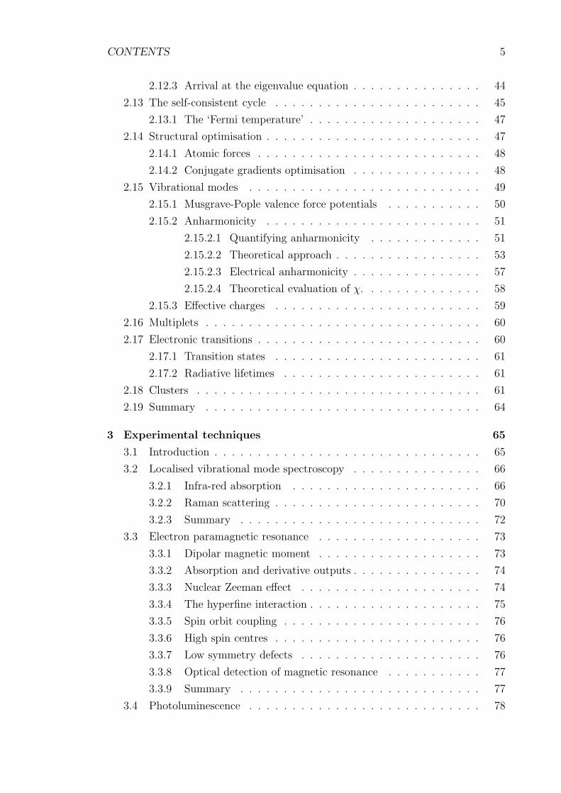
6.3 The variation of the fundamental (a) and overtone (b) frequencies in
cm−1 with the change in the equilibrium C-H length (A) in HCN.
Curve (c) shows the the fundamental frequency ×2 and its difference
from (b) demonstrates that the anharmonicity varies slowly with the
C-H length. The horizontal lines show the experimental frequencies
(3312 and 6521.7 cm−1) [191]). . . . . . . . . . . . . . . . . . . . . . 146
LIST OF FIGURES 17
6.4 (a) Potential energy (au) versus displacement from equilibrium, x,
(au) for C-H stretch in GaAs. The oscillator wavefunctions for the
ground (b), first (c) and second (d) excited states are also shown.
The horizontal lines show the energies of these states. . . . . . . . . 148
6.5 The variation of the fundamental (a) and overtone (b) frequencies in
cm−1 with the change in the equilibrium C-H length (A) for C-H in
GaAs. Curve (c) shows the the fundamental frequency ×2 and its
difference from (b) demonstrates that the anharmonicity varies slowly
with the C-H length. The horizontal line shows the experimental
frequency (2635.2 cm−1 [51]) . . . . . . . . . . . . . . . . . . . . . . 149
6.6 Curve (a) shows the dipole moment of the cluster (au) versus the
change in the equilibrium C-H length (A) for GaAs. Curve (b) shows
the product of oscillator wavefunctions Ψ0(x)Ψ2(x) shifted vertically
upwards. . . . . . . . . . . . . . . . . . . . . . . . . . . . . . . . . . 150
6.7 The intensity of the overtone versus the degree of electrical anhar-
monicity λ. The C-H length is 1.126 A in curve (a) and 1.161 A in
curve (b). . . . . . . . . . . . . . . . . . . . . . . . . . . . . . . . . 151
6.8 Schematic diagram of the C2H defect thought to be responsible for
the 2688 cm−1 band as suggested in Ref.[216]. . . . . . . . . . . . . 153
6.9 Schematic diagram of the three configurations of the C2H defect. 1,
2, and 3 label bond centred sites in which the H atoms have been
sited in this study. . . . . . . . . . . . . . . . . . . . . . . . . . . . 154
6.10 Schematic diagram of seven configurations of the C2H2 defects ex-
amined in this paper. The H sites are labelled using the numbers
1-7, and they can be paired into seven unique defect configurations
as follows: (1,2), (1,3), (1,4), (3,5), (3,6), (4,5), and (6,7). . . . . . . 154
B.1 A diagram showing the splittings of a t2-level with C3v and C2v dis-
tortions to illustrate the Jahn-Teller effect. . . . . . . . . . . . . . . 166

‘Of bell or knocker there was no sign; through these frowning walls and
dark window openings it was not likely that my voice could penetrate.
The time I waited seemed endless, and I felt doubts and fears crowding
upon me. What sort of place had I come to, and among what kind of
people? What sort of grim adventure was it on which I had embarked?’
Extract from ‘Dracula’, Bram Stoker.

Chapter 1
Introduction
Beatrice: ‘You kill me to deny it, but a man of science hath no better
grasp of English than a lawyer doth ethics.’
‘Much Ado About Nothing’, William Shakespeare.
Presented within this thesis are the results of first principles calculations of
the geometry, electronic structure, and optical properties of a variety of defects in
diamond, silicon and GaAs.
‘First principles’ refers to the fact that no experimental data is required as in-
put for the calculations, except for the atomic numbers of the constituent atoms.
This is in contrast to a number of alternative methods, such as the ‘complete ne-
glect of differential overlap’ (CNDO) and similar approximations (INDO, MNDO,
MINDO, etc.) which use (for example) ionisation energies and electron affinities to
parameterise some of the integrals. Simple potential methods such as those due to
Keating [1] and Tersoff [2] are derived from bulk properties. These have the advan-
tage that they can be used to treat large systems very quickly, but suffer from the
fact that the potentials are not sufficiently transferable: that is they do not describe
atomic environments that differ very much from that of bulk. It is therefore highly
desirable to pursue the first principles approach. Until relatively recently, this has
proved difficult for a number of reasons.
The original approach due to Hartree and Fock [3] uses an anti-symmetric wave-
function made up from one-electron states to model a system of N -electrons. How-
ever, this approach suffers from a crippling scaling problem so that in practice only
very small systems are tractable problems. This obstacle was overcome to some ex-
tent by Hohenberg and Kohn [4], and Kohn and Sham [5] who formulated density
functional theory (DFT). Under this approach a system of atoms can be repre-
sented simply from the electron density n(r) instead of the complex anti-symmetric
wavefunctions adopted in Hartree-Fock and related methods.
19

CHAPTER 1. INTRODUCTION 20
A difficulty remains in the computation of the exchange and correlation energies.
This is usually circumvented by invoking the local density approximation (LDA),
where the exchange-correlation energy density at a point r with density n is taken
to be that of the homogeneous electron gas with the same electron density. This
can be readily extended to spin-polarised systems and is then termed the local spin
density approximation (LSDA).
In the past decade the availability of faster, more powerful computing resources
has made possible the study of larger and more challenging problems. These include
the determination of the most energetically favourable surface reconstructions [6, 7],
the geometry of dislocations [8], as well as a plethora of point defect structures.
The LSDA can be applied to DFT in a number of ways, and the code used
throughout this thesis has been named AIMPRO - Ab initio modelling program.
AIMPRO uses a real space approach, which makes the code ideal for the calculation
of the structures of molecules, such as C60 [9] and ferrocene [10]. In the case of
defects however, a cluster must be constructed that is sufficiently large that the local
environment of the defect closely resembles that of the bulk material. Typically,
the clusters used in this thesis contain 70-200 atoms. A schematic representation of
a 71-atom tetrahedral cluster (atom centred) is shown in Fig. 1.1. In AIMPRO the
[110]-[001]
[110]
Figure 1.1: Diagram showing the 71-atom tetrahedral cluster (X35H36).
Kohn-Sham orbitals are expanded in a basis of Gaussian functions, as is the fit to the
charge density. The electron-ion interaction is treated using the norm-conserving

CHAPTER 1. INTRODUCTION 21
pseudopotentials of Bachelet, Hamann, and Schluter [11], except for the case of
hydrogen, for which the bare Coulomb potential is used. The structure is optimised
from the analytically derived forces using a conjugate gradients algorithm.
Using this approach, a number of experimentally measurable quantities can be
obtained. These include localised vibrational modes, the symmetries1 of the ground
and excited states in optical transitions, and semi-qualitatively the transition en-
ergies and radiative lifetimes. Thus, AIMPRO can be used not only to examine
the detailed structures of defects to correlate with experiment, but also provide
information to experimentalist colleagues as a guide to where to look for, for ex-
ample, a one-phonon side band in photoluminescence. In fact, collaboration with
experimental groups has proved highly productive in a number of cases such as the
T-line [12] and the hydrogenated vacancy and interstitial [13] in Si.
The contents of this thesis can be summarised as follows. Chapter 2 describes in
some detail the background to the theory, touching on Hartree-Fock methods, and
parameterised Hartree-Fock methods (especially CNDO). However, the main aim is
to discuss the AIMPRO formalism. The methods and approximations adopted for
the calculations of experimental observables are detailed in this Chapter and their
limitations explained.
Following this, Chapter 3 outlines a number of the more commonly used exper-
imental techniques. These are: localised vibrational mode spectroscopy, electron
paramagnetic resonance (EPR), luminescence spectroscopy techniques, and deep
level transient spectroscopy.
The background Chapters are followed by three Chapters containing the results
of the ab initio calculations. The first (Chapter 4) concerns the class of vacancy-
related optical defects in diamond formed particularly after irradiation and anneal-
ing. They are characterised by strong and sharp optical peaks, and are made up
of vacancies complexed with one or more impurity atoms. Good agreement with
experiment is found in the case of a single N atom in the neutral or negative charge
states. The quantitative agreement in the case of three N atoms is slightly less
satisfactory, although the calculations have provided a clear qualitative picture.
Si and P both readily complex with a vacancy and form a split-vacancy structure.
The former gives rise to a complex set of zero-phonon lines, which can be understood
from a negative charge state of the centre. The latter may be responsible for a broad
red donor-acceptor recombination band, but much more importantly is likely to lie
at the root of the difficulty in producing n-type semiconducting diamond using
phosphorus.
1The character tables of the key point groups studied in this thesis are given in Appendix A.
CHAPTER 1. INTRODUCTION 22
The location and presence of H in diamond has long been a matter of heated
discussion. Following recent observation of H-related centres in polycrystalline di-
amond using EPR, the structure and electronic properties of vacancy-hydrogen
complexes are also presented in Chapter 4, but no firm conclusions can be made
regarding this class of centres.
Chapter 5 continues the theme of luminescent centres in diamond. Diamonds
which are produced using the high temperature, high pressure method exhibit pro-
nounced optical peaks. Many of these have been correlated with Ni introduced from
the solvent-catalyst. Ni is known to give rise to a number of EPR signals, and a
number of assignments have been made in the past to both substitutional and inter-
stitial Ni centres. The results presented here show that there is no requirement for
an interstitial species, and many assignments may have been made on the strength
of unreliable calculations. The geometries and electronic structures of Ni, Ni-N and
Ni-B centres are reported.
The final section in Chapter 5 examines substitutional Ni and Ni-hydrogen com-
plexes in silicon. In contrast with diamond, Ni−s in Si is known to undergo a Jahn-
Teller distortion to form a low symmetry centre. This is reproduced in these calcu-
lations. Furthermore, evidence is provided for hydrogen adopting the anti-bonding
site in the Ni-H2 complex.
The final results Chapter concerns a range of centres that have been observed in
GaAs using infrared absorption spectroscopy. C is a common impurity, and is often
intentionally introduced as an acceptor due to its low diffusivity and high doping
concentrations. However, hydrogen readily complexes with C to form electrically
inactive centres. This CAs-H centre exhibits a characteristic local vibrational mode
at 2635 cm−1. However, the isotope shifts suggest that this mode is very anhar-
monic. It is anharmonicity that breaks the symmetry selection rules that prevent an
overtone, but to date, the overtone to this centre has not been observed. Chapter 6
shows that one solution may be that electrical anharmonicity reduces the intensity
of the overtone.
A further set of bands related to C-H stretch modes have been seen in heavily
doped samples. Interestingly, some of them exhibit strong (nearly 100%) polarisa-
tion in one of the two 〈110〉 directions normal to the growth direction. It is thought
that C-pairs are formed during growth, and H bonded to one of these C atoms gives
rise to the polarised absorption. The structures and local vibrational modes of a
number of such centres with one or two hydrogen atoms are reported.
General conclusions are presented in Chapter 7.
Chapter 2
Theory
‘As far as the laws of mathematics refer to reality, they are not certain;
and as far as they are certain, they do not refer to reality.’
- Albert Einstein
2.1 Introduction
A variety of theoretical methods and approximations are used by the academic
community to model many-body problems. In this Chapter, I shall start from stat-
ing the initial problem, and step through the construction of a number of methods
adopted to solve it. Starting with the Born-Oppenheimer approximation, I shall
outline Hartree-Fock theory (Sec. 2.4), and a number of parameterised Hartree-Fock
methods (Sec. 2.5) which are based on the Roothaan equations. Finally I shall out-
line density functional theory (Sec. 2.8) and the local density approximation for the
exchange-correlation energy (Sec. 2.9).
However, the main goal of this Chapter is to detail the approximations and
techniques employed in the ‘Ab Initio Modelling PROgram’ or AIMPRO. AIMPRO
is a self-consistent density functional code applied to a real-space atomic-clusters
developed in Exeter and Newcastle over the last ten years. The use of atomic clusters
makes the program ideally suited to calculations of molecular structures and has
been successfully applied to the class of carbon structures termed ‘fullerenes’ [9].
However, the main thrust of this thesis is to explore the properties of defects in
solids. AIMPRO models bulk-material with large clusters (typically 70-150 atoms)
where the surface ‘dangling bonds’ are saturated with hydrogen atoms. The charge
density and wavefunctions are expanded in terms of a Gaussian basis, and models
the electron-ion interaction via norm-conserving pseudopotentials (Sec.2.11).
AIMPRO can currently calculate a number of experimental observables, includ-
ing localised vibrational modes, and electronic transition energies and rates. The
23

CHAPTER 2. THEORY 24
methods used are outlined in Sec. 2.15 and Sec. 2.17 respectively. Other observ-
able quantities that may be estimated using AIMPRO are binding energies, and
reorientation and migration barriers. The AIMPRO methodology is reviewed in
Ref. [14].
2.2 The problem posed
Fundamentally, we wish to solve the many-body Schrodinger equation for a specific
set of atoms in a specific configuration, i.e.
HΨi = EiΨi,
where H is the many-body Hamiltonian, and Ψi is the many-body wavefunction
corresponding to the ith state which has energy Ei. In general, Ψi is a function of
the electron spin and co-ordinates as well as the nuclear positions. For all but the
most simple of problems, this is an intractable problem.
Adopting atomic units1 the Schrodinger equation for a set of electrons in a field
due to ions of charge Za at sites Ra is given by:−
∑a
1
2Ma∇2
a −1
2
∑µ
∇2µ +
1
2
∑ν 6=µ
1
|rµ − rν | −∑µ,a
Za
|rµ − Ra|
+1
2
∑a6=b
ZaZb
|Ra − Rb| − E
Ψ(r) = 0. (2.1)
This can alternatively (using obvious notation) be written as
Tion + Te + Ve−e + Ve−i + Vi−i −EΨ(r) = 0. (2.2)
Here r is used to denote the positions and the spins of the electrons, i.e. (r1, s1, r2, s2,
r3, s3, ...).
Any practical method of solving Eq. 2.1 must first decouple the motion of the
electrons and ions. One may then calculate the effective potential felt by each
electron due to the other electrons and ions. From there one may calculate the
forces on the ions, optimise the ion positions with respect to the total energy, and
hence derive the equilibrium geometry.
Returning to the first step, one needs to separate the electron and ion compo-
nents of the many-body wavefunctions, and this is achieved under the adiabatic or
Born-Oppenheimer approximation.
1In the atomic units system, ~, e, me, and 4πε0 are taken to be unity. Then, 1 a.u. of energyis equivalent to 27.212 eV, and 1 a.u. of length is 0.529 A.
CHAPTER 2. THEORY 25
2.3 The Born-Oppenheimer approximation
One assumes that, due to the large mass of the ions compared to that of the electron,
the motion of the ions simply modulates the electronic wavefunction, i.e.
ΨTotal(r, R) = χ(R)Ψ(r, R). (2.3)
Here χ(R) is an amplitude dependent on the positions of the ions, and Ψ(r, R) is a
solution of
Te + Ve−e + Ve−i + Vi−i − EΨ(r) = 0.
R denotes the nuclear co-ordinates (R1,R2, ...). Substituting Eq. 2.3 into Eq. 2.2,
multiplying through by Ψ∗(r, R) and integrating over r, one arrives at the equation:
Tion(R) + E(R) +W (R) −ETχ(R) =∑a
∫Ψ∗(r, R)
1
Ma
∇aΨ(r, R)∇aχ(R)dr. (2.4)
The sum is over the nuclei. The left hand is simply the Schrodinger equation for
the ions moving in a potential E +W , where
W (R) = −∑
a
1
2Ma
∫Ψ∗(r, R)∇2
aΨ(r, R)dr
is due to the electrons moving along with the nuclei. W (R) is negligibly small.
The right hand side of Eq. 2.4 is zero if Ψ(r, R) is real and corresponds to a non-
degenerate ground state. Otherwise this term is a small perturbation, which can be
important in the case of a degenerate ground state. Here it can lead to symmetry
breaking as in the case of a Jahn-Teller distortion [15]. If the right hand side is
neglected, then the electron and ion motions are decoupled.
The term E(R) represents the potential energy of the ions averaged over the
state Ψ(r, R), and the minimum of E therefore represents the ground state of the
system. This is usually what one seeks in these calculations.
2.4 Hartree-Fock Theory
One way to construct the many-body wavefunction, Ψ(r, R), is from a single Slater
determinant of N one-electron spin-orbitals2:
Ψ(r) =1√N !
det |ψµ(r)|, ψµ(r) = ψ(r)χα(s).
2The determinant form of the wavefunction ensures that the anti-symmetry under particleexchange, required by the Pauli exclusion principle, is included.

CHAPTER 2. THEORY 26
χα(s) is a spin function which satisfies:∑s
χ∗α(s)χβ(s) = δαβ ,
with the sum over up and down spins, and the orbitals satisfy:∫ψ∗
i (r)ψj(r)dr = δij .
In each case δ is the standard Kronecker delta function.
The averaged energy of a such determinental wavefunction is, adopting Dirac
notation, 〈Ψ|H|Ψ〉. This has been shown [16] to be given by:
E =∑
λ
〈λ|T + Ve−i + Vi−i|λ〉 +1
2
∑λ,µ
〈λµ|Ve−e|λµ〉 − 〈λµ|Ve−e|µλ〉, (2.5)
where the sums are over the occupied spin-orbitals. Note, the second summation
involve four-centre integrals. Alternatively, Eq. 2.5 may be written as:
E = −1
2
∑λ,s
∫ψ∗
λ(r, s)∇2ψλ(r, s)dr +
∫n(r)Ve−idr + EH + Ex + Ei−i, (2.6)
where we have introduced the Hartree, exchange, and ion-ion energies (EH, Ex, and
Ei−i), and the electron density, n:
EH =1
2
∫n(r1)n(r2)
|r1 − r2| dr1dr2, (2.7)
Ex = −1
2
∑λµ
∑s1s2
∫ψ∗
λ(r1)ψ∗µ(r2)
1
|r1 − r2|ψµ(r1)ψλ(r2)dr1dr2, (2.8)
Ei−i =1
2
∑a6=b
ZaZb
|Ra −Rb| , and (2.9)
n(r) =∑λ,s
|ψλ(r, s)|2. (2.10)
The total energy (for a given set of nuclei), E, is then minimised subject to or-
thonormal ψλ by introducing Lagrange multipliers Eλµ, giving the Hartree-Fock
(HF) equations for each orbital λ:−1
2∇2 + Ve−i(r) + V H(r) + V x
λ (r) − Eλ
ψλ(r) =
∑µ6=λ
Eλµψµ(r). (2.11)
Here
V H(r)ψλ(r) =δEH
δψ∗λ
=
∫n(r1)ψλ(r)
|r− r1| dr1,
V xλ (r)ψλ(r) =
δEx
δψ∗λ
= −∑µs1
∫ψ∗
µ(r1)ψλ(r1)1
|r− r1|ψµ(r)dr1

CHAPTER 2. THEORY 27
are the Hartree and exchange potentials respectively, and the expression for the
exchange involves a sum over occupied orbitals µ whose spin are the same as that
of λ.
Next, one performs a unitary transformation on the Slater determinant to diag-
onalise Eλµ reducing the right hand side of Eq. 2.11 to zero. The total energy can
then be found by multiplying the HF equations (2.11) by ψ∗λ(r), integrating over r
and summing over λ and s, to give:
−∑λ,s
∫ψ∗
λ(r)1
2∇2ψλ(r)dr +
∑λ,s
∫ψ∗
λ(r)Ve−i(r)ψλ(r)dr
+∑λ,s
∫ψ∗
λ(r)VH(r)ψλ(r)dr +
∑λ,s
∫ψ∗
λ(r)Vxλ (r)ψλ(r)dr−
∑λ,s
Eλ = 0
Then, the first and second terms are the kinetic energy associated with the elec-
trons and the electron-ion interaction energy respectively. The terms involving the
Hartree and exchange potentials are simply twice the Hartree and exchange energies
respectively. Therefore, we now have:
Te + Ee−i + 2EH + 2Ex −∑
λ
Eλ = 0.
Then the total energy is found by removing the double counting and adding the
ion-ion energy term:
Etotal =∑
λ
Eλ − EH − Ex + Ei−i.
In practice the HF equations are solved self-consistently by making a sensible
initial guess at the set of ψλ(r) and calculating the Hartree and exchange potentials.
These output potentials are then fed back into the HF equations to calculate a
new set of ψλ(r). This cycle is repeated until the input and output potentials are
sufficiently close. Usually, the initial guesses for the spin-orbitals are related to
atomic orbitals.
Using HF methods, one can arrive at a very good agreement for structures and
vibrational modes of small molecules. However, a number of four-centre integrals are
required for the exchange energy. This leads to a prohibitively heavy computational
effort for systems of more than a few atoms, and therefore the simulation of defects
in bulk materials is impractical. To apply HF theory to larger problems, a number of
semi-empirical parameterisations have been developed where these time consuming
integrals are no longer calculated, or are performed approximately.

CHAPTER 2. THEORY 28
2.5 Parameterised Hartree-Fock methods
There are a number of paradigms for parameterising the basic HF equations, each
having a different level of approximation. For the purposes of this thesis, only the
basic approximations are outlined. One particular method, the original formulation
of the complete neglect of differential overlap approximation [17], is described in
detail.
The first stage is to expand the one-electron wavefunctions in a linear combina-
tion of atomic orbitals (LCAO), φµ:
ψi =∑
µ
cµiφµ.
Then one can write the (differential) HF equations in an algebraic expression,
termed the Roothaan equations. The Roothaan equations are given by:∑ν
(Fµν − εiSµν) cνi = 0 (2.12)
where Fµν is the Fock matrix and Sµν is the overlap matrix:
Fµν = Hµν +∑λσ
Pλσ
[〈µν|λσ〉 − 1
2〈µλ|νσ〉
](2.13)
Sµν =
∫φµ(r)φν(r)dr
and εi are the one-electron energies. Hµν and Pλσ are the core Hamiltonian ma-
trix elements and the density matrix elements respectively, and 〈µν|λσ〉 are the
differential overlap matrix elements:
Hµν =
∫φµ(r)H
coreφν(r)dr
Pλσ = 2
occ∑i
c∗λicσi
〈µν|λσ〉 =
∫ ∫φµ(r1)φν(r1)
1
|r1 − r2|φλ(r2)φσ(r2)dr1dr2
At this stage there are no approximations. However, one can utilise the fact that
many of the integrals are very small or zero and begin to neglect systematically some
of the matrix elements.
The zero-differential overlap approximation [18] (ZDOA) is the starting point for
many semi-empirical methods. The ZDOA sets all but a few terms in the differential
overlap matrix identically to zero:
〈µν|λσ〉 = 〈µµ|λλ〉δµνδλσ,

CHAPTER 2. THEORY 29
and the overlap integrals, Sµν are neglected in the normalisation of the molecular
orbitals. To retain some of the overlap character that is required to treat chem-
ical bonding correctly, the Hamiltonian matrix elements, Hµν , are treated semi-
empirically.
The ZDOA simplifies the Roothaan equations to become:
∑ν
Fµνcνi = εicµi (2.14)
Fµν =
Hµµ − 1
2Pµµ〈µµ|µµ〉+
∑λ Pλλ〈µµ|λλ〉 ν = µ
Hµν − 12Pµν〈µµ|νν〉 µ 6= ν.
This vastly reduces the number of 2-electron integrals and removes all 3- and 4-
centre integrals. Note, these equations only apply to closed shell molecules, that is
to say spin zero systems. One can extend these equations to a spin polarised system
simply by writing down Eq. 2.14 for each spin.
2.5.1 Complete neglect of differential overlap
The degree to which the ZDOA is applied varies from one method to another,
but the simplest form is the complete neglect of differential overlap approximation,
CNDO [19]. Here Eq. 2.14 applies, but in order that rotational invariance is main-
tained, one is required to further approximate the remaining 2-electron integrals
by:
〈µµ|λλ〉 = γAB,
where γAB is the average electrostatic repulsion between any electron on atom A
and any electron on atom B. Thus, these integrals depend only on the nature of
the atoms A & B, and not on the type of orbitals. Under CNDO, only the valence
electrons are explicitly considered.
Thus the Fock matrix elements for the CNDO approximation are given as:
Fµν =
Hµµ − 1
2PµµγAA +
∑λ PBBγAB ν = µ, φµ on atom A
Hµν − 12PµνγAB ν 6= µ, φµ on atom A, φν on atom B
where PBB =∑B
λ Pλλ is the total electron density associated with atom B. Applying
the same approximations to the core Hamiltonian (H = −12∇2−∑
B VB) one arrives
at:
Hµν =
Uµµ − ∑
B 6=A〈µ|VB|µ〉, ν = µ, φµ on atom A
Uµν −∑
B 6=A〈µ|VB|ν〉, φµ, φν on A⟨µ
∣∣−12∇2 − VA − VB
∣∣ ν⟩− ∑
C 6=A,B〈µ|VC|ν〉, φµ on A, φν on B
(2.15)

CHAPTER 2. THEORY 30
where
Uµν =
⟨µ
∣∣∣∣−1
2∇2 − VA
∣∣∣∣ ν⟩,
and −Vi is the potential due to the nucleus and core electrons on atom i.
If the atomic orbital basis is made up from s, p, d, ... atomic functions, then Uµν ,
µ 6= ν are zero by symmetry. Again, to maintain rotational invariance 〈µ|VB|µ〉must be a constant, VAB, which describes the interaction of any electron on atom
A with the core of atom B. Furthermore, neglect of monatomic differential overlap
means that 〈µ|VB|ν〉 = 0, µ 6= ν. The term involving a summation over C in
Eq. 2.15 is a three-centre integral, and thus is neglected, leaving the first term, called
the ‘resonance integral’, which is a measure of the possible lowering of the electron
energy by existing simultaneously in the fields of two atoms. Rotational invariance
requires that this term is a constant βµν , which is assumed to be proportional to
the overlap, i.e. βµν = βoABSµν .
Applying these further conditions to Eqs. 2.15, we arrive at
Hµν =
Uµµ − ∑
B 6=A VAB, ν = µ, φµ on A
0, µ 6= ν, φµ, φν both on A
βoABSµν , µ 6= ν, φµ on A, φν on B
(2.16)
This expression can now be substituted into the Fock matrix, giving
Fµν =
Uµµ +
(PAA − 1
2Pµµ
)γAA +
∑B 6=A(PBBγAB − VAB) ν = µ
βoABSµν − 1
2PµνγAB µ 6= ν
(2.17)
One can write the summation in Eq. 2.17 as∑B 6=A
−QBγAB + (ZBγAB − VAB),
where QB is the net charge on atom B. Here (ZBγAB − VAB) is the difference
between the potentials due to the valence electrons and core of atom B, termed the
penetration integral [20]. This demonstrates one of the advantages of this approach:
physical quantities are readily separable allowing simple interpretation of the results
of any calculation.
Finally, combining all the approximations, an expression for the total energy
can be written down:
Etot =1
2
∑µν
Pµν(Hµν + Fµν) +∑A<B
ZAZBR−1AB.
Now one must decide how to evaluate an number of terms: Sµν , Uµν , VAB,
γAB, and βoAB. Under the CNDO approximations there are historically two systems
adopted, termed CNDO/1 and CNDO/2.

CHAPTER 2. THEORY 31
2.5.2 CNDO/1
• The overlap integrals are directly evaluated. The repulsion integrals are ap-
proximated by integrals of s-orbitals on atoms A and B:
γAB =
∫ ∫s2
A(r1)1
|r1 − r2|s2B(r2)dr1dr2.
• The electron-ion interaction VAB is also calculated using an s-orbital on atom
A:
VAB = ZB
∫s2
A(r)
|r − RB|dr.
• The one-electron Hamiltonian matrix elements, Uµµ, are obtained by fitting
to atomic ionisation energies.
• Finally, the bonding parameters, βoAB are approximated by the expression
βoAB =
1
2(βo
A + βoB),
and each βoA is empirically fitted to ab initio calculations for each atomic
species.
CNDO/1 was the first parameterisation under the CNDO approximation, but
this was quickly superseded by CNDO/2.
2.5.3 CNDO/2
There are two improvements made to the CNDO/1 parameterisation.
1. The penetration integral is neglected which means that the electron-ion in-
tegrals VAB are no longer evaluated separately, but instead are related to
the repulsion term, VAB = ZBγAB. There is no physical justification for this
approximation, but it often predicts bond-length reasonably well.
2. Instead of fitting the Uµµ using only the ionisation potential, an average of the
ionisation potential and electron affinities is used. This should make CNDO/2
better suited to modelling the tendencies for atomic orbitals to both gain and
lose electrons than CNDO/1.
In all other ways CNDO/2 is the same as CNDO/1.
In summary, CNDO-type calculations are based on the HF quantum mechanical
description. The approximations neglect the vast majority of integrals, making the
calculation of large systems of atoms possible. However, in the process a great deal

CHAPTER 2. THEORY 32
of the interaction information is lost. The fact that the method has been successful
in describing a range of problems is primarily due to the fact that fitting some of
the terms to experimental and/or ab initio data in some way replaces the neglected
terms by building the information into the integrals that remain.
It should be noted, however, the neglect of exchange integrals means that spin-
sensitive systems will not be correctly described. This is in some part corrected by
the following method.
2.5.4 Intermediate neglect of differential overlap
CNDO explicitly excludes the two-electron exchange integrals. These are crucial
to provide a description of any system where an electron spin distribution is im-
portant such as finding the relative energies of different spin states. If one includes
exchange for electrons on the same atom, i.e. one retains one-centre monatomic dif-
ferential overlap integrals, this problem is mitigated to some extent and is termed
the intermediate neglect of differential overlap, (INDO) [21, 22]. In the formalism
of Slater [23], these integrals are established by using a fit to experimental atomic
energy levels. There are no other major differences between CNDO and INDO.
2.5.5 Neglect of diatomic differential overlap
The next logical extension is to neglect only diatomic differential overlap, and thus
such a method would include dipole-dipole interactions of the form 〈sApA|sBpB〉.This level of approximation is naturally termed the neglect of diatomic differential
overlap, (NDDO).
2.5.6 Summary
In summary, these approximate, empirical methods have been developed to circum-
vent the prohibitive computational demands of the ab initio HF method. Although
the approximations allow one to treat large systems of atoms very rapidly, terms in
the calculations are being sacrificed for this speed, and consequently the description
of a system of atoms using these methods will always be inferior to first principles
methods.
One example of where this can be important is where CNDO methods get the
ordering of electronic levels wrong. This is the case for the negatively charged
substitutional Ni impurity in diamond [24] where CNDO calculations produce a
rogue a1 level below instead of above a t2 level. This leads to the defect possessing
an effective spin of S=1/2, whereas experimental evidence shows that the true spin
state is S=3/2 [25].

CHAPTER 2. THEORY 33
2.6 Hartree-Fock theory of the homogeneous elec-
tron gas
As stated above, HF theory can only be applied to simple systems. One such situ-
ation is the homogeneous electron gas, where the ions form a uniform background.
A solution to Eq. 2.11 then takes the form of a set of plane waves of the form,
ψλ(r, s) =1√Ωeik.rχα(s),
where λ labels the wave-vector k and spin α, and Ω is the volume of the primitive
unit cell. Since the electron density, n, is uniform, EH and Ei−i exactly cancel Ee−i
to give the energy levels:
Eλ = Ek,α =1
2k2 + V x
k .
It can be shown that by writing η = k/kf (where the electron density is given by
n = 13π2k
3f), the exchange potential is:
V xk = −4
(3n
8π
) 13
F (η),
F (η) =1
2+
1 − η2
4ηln
(1 + η
1 − η
).
Since the density of states is given by
N(E) =4πk2
8π3
1
|∇Ek| ,
the singularity in the derivative of V xk as η → 1 leads to a zero density of states as
k → kf , which is incorrect, and is due to the absence of correlation in the calcu-
lations. This error can be surmounted by constructing wavefunctions made up of
combinations of determinants, a method which is termed ‘configuration interaction’
(CI), but this is extremely computationally demanding and only a few atoms can
be treated in this manner.
2.7 Correlation
In 1980, Ceperley and Alder [26] performed quantum Monte-Carlo calculations on
the non-spin-polarised and spin-polarised electron gases to find a better estimate of
the ground state energies. This method includes the correlation energy, Ec which
is missing from HF. Defining the correlation energy per electron, εc, polarisation ξ
and the Wigner-Seitz radius of each electron rs by:
Ec = Ωnεc(n, ξ), ξ =(n↑ − n↓)
n, rs = (4πn/3)1/3, (2.18)

CHAPTER 2. THEORY 34
γ β1 β1
Non-polarised -0.1423 1.0529 0.3334Polarised -0.0843 1.3981 0.2611
A B C DNon-polarised 0.0311 -0.0480 0.0020 -0.0116Polarised 0.0155 -0.0269 0.0007 -0.0048
Table 2.1: Parameterisation of the exchange-correlation energy in Ref. [27].
then εc for ξ = 0 and ξ = 1 are given as [27]:
εc =
γ1 + β1
√rs + β2rs−1, for rs ≥ 1
B + (A+ Crs) ln(rs) +Drs, for rs < 1
The values of the coefficients are given in Table 2.1.
In the case of a partially polarised gas, i.e. where 0 < ξ < 1, the correlation
energy is taken to be the average over the polarised and non-polarised cases [28]:
εc(n, ξ) = εnpc (n) + f(ξ)(εpc (n) − εnp
c (n))
f(ξ) =(1 + ξ)4/3 + (1 − ξ)4/3 − 2
24/3 − 2.
To a good approximation, the exchange-correlation energies vary as αns1 and βns2
for the non- and fully-polarised cases respectively, and AIMPRO uses the simplified
expression for the non-polarised case Exc:
Exc = ΩAn1.30917, (2.19)
For polarised gases, AIMPRO uses:
Exc = Ω∑i,s
Ainpi+1s nqi
1−s, (2.20)
where Ai, pi and qi are given in Table 2.2. The subscript 1−s in Eq. 2.20 refers to the
opposite spin to that over which is being summed. The error in this approximation
is very small for low electron density (n < 1), but for larger density values, an
alternative set of parameters is used A′i, p
′i and q′i (also given in Table 2.2). However,
this approximation is poorer at low densities.
2.8 Density functional theory
If one wishes to perform first principles calculations for large systems of atoms, one
needs to circumvent the computationally intensive aspects of HF theory in some
way. One solution which has been highly successful over the past decade is density

CHAPTER 2. THEORY 35
i Ai pi qi1 -0.9305 0.3333 0.00002 -0.0361 0.0000 0.00003 0.2327 0.4830 1.00004 -0.2324 0.0000 1.0000i A′
i p′i q′i1 -0.9305 0.3333 0.00002 -0.0375 0.1286 0.00003 -0.0796 0.0000 0.1286
Table 2.2: Parameterisation of the exchange-correlation used in AIMPRO.
functional theory (DFT). At the centre of this method the electron density is treated
as the fundamental variable [4, 5] instead of the one-electron wavefunctions as in
HF. This is possible since there is a one-to-one correspondence between the a non-
degenerate, non-polarised ground state wavefunction, Ψ(r) and the electron density
n(r1) defined by the expression:
n(r1) =∑
µ
∫δ(r1 − rµ)|Ψ(r)|2dr.
This in turn arises from the result that for the electron Hamiltonian, H = Te+Ve−e+
Ve−i, there is a one-to-one correspondence between the external potential Ve−i and
the ground state electron density. This can be easily proved as follows. Suppose
that this is not true, i.e. there exist two potentials with the same n. Then, from the
variational principle, if Ψ1 and Ψ2 are the ground state (normalised) wavefunctions
for the two potentials V1 and V2 with density n, and if HiΨi = EiΨi, then
E1 = 〈Ψ1|H1|Ψ1〉 < 〈Ψ2|H1|Ψ2〉 = E2 + 〈Ψ2|V1 − V2|Ψ2〉= E2 +
∫(V1 − V2)n(r)dr.
But similarly
E2 < E1 +
∫(V2 − V1)n(r)dr.
Adding these equations gives us
E2 + E1 < E1 + E2,
which is a contradiction. Thus, Ve−i is uniquely defined by n, and hence Ψ is a unique
functional of n. Remarkably, this means that the many-body wavefunction which
is dependent on (3 spatial +1 spin)×(number of electrons) variables is uniquely
defined by the charge density which is a function of only three spatial variables and
spin.

CHAPTER 2. THEORY 36
It has also been shown [4] that the total energy, E, is also a functional of the
electron density:
E[n] = T [n] + Ee−i[n] + EH[n] + Exc[n] + Ei−i, (2.21)
where
Ee−i[n(r)] = −∫n(r)
∑a
Za
|r − Ra|dr,
EH[n(r)] =1
2
∫n(r1)n(r2)
|r1 − r2| dr1dr2,
Ei−i =1
2
∑a6=b
ZaZb
|Ra − Rb| .
The expressions for the kinetic energy, T , and the exchange-correlation energy,
Exc, are not obviously functionals of n in the way Ee−i and EH are. Kohn and
Sham [5] provided a paradigm for treating the kinetic term by introducing a set of
orthonormal orbitals3 as a basis for the (spin polarised) charge density:
ns(r) =∑
λ
δsλ,s|ψλ(r)|2.
Then the kinetic energy can be written as
T = −1
2
∑λ,s
∫ψ∗
λ∇2ψλdr.
The only remaining term in Eq. 2.21 is Exc. An exact expression for this is
not known, so in practice some form of approximation must be adopted, the most
common of which is termed the local density approximation (LDA).
2.9 The local density approximation
One assumes that for any small region in the system, the exchange-correlation
is the same as that for the uniform electron gas with the same electron density.
This approximation applies to a spin zero system, and the exchange-correlation is
approximated by:
Exc =
∫n(r)εxc(n)dr,
where εxc(n) is the exchange-correlation density for the homogeneous electron gas.
For a spin polarised system, one simply applies the same assumptions using the
exchange-correlation energy density of the spin-polarised electron-gas, εxc(n↑, n↓).3Note, since these ‘Kohn-Sham’ (KS) orbitals are merely an expansion of the charge density,
strictly they cannot be interpreted as one-electron states.

CHAPTER 2. THEORY 37
This is termed the local spin density approximation (LSDA) and implementing this
within DFT is often termed local spin density functional theory (LSDFT).
It is possible to go beyond the local approximation, and include further deriva-
tive terms in the density, termed the gradient correction [29]. However, the merits
of such an approach are not accepted universally: with the improvement in ground
state energy the gradient correction generally leads to a deterioration in the struc-
ture.
2.10 Determination of the Kohn-Sham orbitals
The KS orbitals are determined by minimising the total energy, E, with respect to
ns, subject to the constraint that both the total spin and the number of electrons are
conserved. Then applying the variational principle, one arrives at the KS equations:−1
2∇2 −
∑a
Za
|r− Ra| + V H(r) + V xcsλ
(n↑, n↓) −Eλ
ψλ(r) = 0
∑s
∫|ψλ(r)|2dr = 1,
where
V xcs =
d(nεxc)
dns.
These sets of equations (one set for each spin state) can be solved to generate the
KS levels, Eλ, and KS wave-functions. In contrast to HF, the wavefunctions derived
are not strictly those belonging to one-electron states, and the eigenvalues under
LSDFT are not the ionisation energies as is the case in HF theory (Koopman’s
theorem), but instead are related to the quasi-particle energies. It is possible to
augment the density functional theory via, for example, GW theory4 which predicts
quasi-particle energies with reasonable accuracy [31].
2.11 Pseudopotentials
In practice, the all-electron potential representing the interaction between the nuclei
and electrons is replaced by a pseudopotential, in which only the valence electrons
are considered explicitly. This approximation can be crucial since a treatment
including core states has a number of associated difficulties.
4A full discussion of GW theory is beyond the scope of this thesis, but the framework withinwhich the GW approximation is formulated is that of a perturbation expansion of one particlegreens function G(p, w). See for example Ref. [30]

CHAPTER 2. THEORY 38
• First, the total energy generated by using an all-electron potential is very
large. Then when comparing total energies of similar systems large errors can
be generated by subtracting similar values.
• Secondly, as one adds more and more core electrons, wavefunction orthonor-
mality means that the wavefunctions will become very oscillatory. This makes
the fitting to a Gaussian or plane-wave basis very difficult. Furthermore, a
small error in the fit to the wavefunction for one of the core states can have
a dramatic effect on the energy of the core eigenvalue.
• Thirdly, as the atomic number increases, the core states become relativistic
in nature. The use of pseudopotentials immediately removes this difficulty.
Since the core electrons do not take a significant role in bonding, one can justify the
use of pseudopotentials in solid state problems. However, the core electrons undergo
exchange interactions with the valence electrons, the constructions of pseudopoten-
tials is a non-trivial exercise.
The way one goes about constructing a pseudopotential is dependent on the
application for which the potential is to be used. For example, for a plane-wave
approach, one would desire a functional form that decays rapidly with wave-vector,
such as the soft-pseudopotentials of Vanderbilt [32], but this is not important in
the real-space methodology adopted in AIMPRO.
We have adopted the approach of Bachelet et al. [11] who developed a set of
norm-conserving pseudopotentials for atomic species with atomic number ranging
from 1 (hydrogen) to 94 (plutonium). The term ‘norm-conserving’ simply implies
that the pseudopotential possesses exactly the same atomic charge density beyond
the core radius as that of the the all-electron potential.
The sequence of processes required to produce a potential is as follows:
1. The KS equations are solved for the atom. To do this, the spherically sym-
metric atomic configuration is chosen so that the KS levels are labelled by
angular momentum, l, in the case of the lighter atoms, and j = l±1/2 for the
heavy atoms where the Dirac equation is required. It is important to include
in the construction all the orbitals that will take part in bonding the solid
state. For example, in the case of carbon, the atomic configuration is nor-
mally taken as 1s22s22p2, which does not contain any d-orbital dependence.
To rectify this, the l = 2 potential is constructed using the ionised configura-
tion 1s22s0.752p13d0.25. This procedure is tailored to each atomic species.
2. Then, the solutions to the all-electron KS equations for the atom produce a set
of all-electron wavefunctions and energy levels, which in turn can construct the

CHAPTER 2. THEORY 39
all electron potential, denoted V ν(r). This potential contains the exchange-
correlation, Hartree and nuclear potentials, and is singular at r = 0.
3. From these all-electron quantities, one constructs a first approximation to the
pseudopotential for each value of the angular momentum, l, or in the case of
relativistic treatment, j = 1 ± 1/2. This first guess removes the singularity:
Vl(r) = V ν(r)(1 − f(r/rc,l)) + cνl f(r/rc,l).
The function f(x) tends to unity as x→ 0, and rapidly decreases to zero as x
increases. Such a function might be e−x3.5. Then, Vl(r) → cνl as r → 0, where
cνl is a constant chosen so that the lowest energy level generated by V ν is the
same as that generated by Vl(r). Then the normalised pseudo-wavefunction
of Vl, denoted by ων1l, is, to within a normalisation constant, the same as the
true, all-electron wavefunction at large r, since Vl(r) is the same as V ν(r)
there.
4. rc,l is the radius at which the pseudo-wavefunction and true wavefunction
approach each other, and is termed the core radius. Care must be taken in
the choice of value for rc,l since taking too large a value will remove critical
bonding information from the potential. Generally, rc,l is chosen to be midway
between the last node and last extremum.
5. The next stage is to modify the pseudo-wavefunctions so that they agree with
the true wavefunctions exactly, and not just to a normalisation constant. This
is done using the expression:
ων2l = γν
l ων1l(r) + δν
l rl+1f(r/rc,l).
Here the quantities γνl and δν
l are simply the normalisation constants.
6. The potential that gives rise to the pseudo-wavefunction ων2l is obtained by
inverting the Schrodinger equation using the energy levels of the all-electron
system. Such a potential would then give rise to a wavefunction that agrees
with the all electron wavefunction outside the core radius, and also generates
the all-electron energy levels. However, this potential still includes the Hartree
and exchange-correlation potentials.
7. The Hartree potential arising from the pseudo-wavefunction can be removed
exactly, but a removal of the exchange-correlation potential can only be per-
formed approximately. This approximation can be improved upon by instead
subtracting the exchange-correlation potential due to the all-electron charge

CHAPTER 2. THEORY 40
density and spin-polarisation [33]. Once this is done, one is left with the bare
electron-ion pseudopotential, Vl(r).
8. For relativistic atoms, an average pseudopotential is defined as being:
Vl(r) =1
2l + 1
lVl− 1
2(r) + (l + 1)Vl+ 1
2(r)
,
which is termed the scalar relativistic potential. The spin-orbit potential is
given by:
V sol (r) =
2
2l + 1
Vl+1/2(r) − Vl−1/2(r)
,
which leads to the full pseudopotential:
V ps(r) =∑
l
|l〉 Vl(r) + V sol (r)L.S 〈l|.
9. Finally, the potentials have been parameterised by fitting to simple functions,
such that:
Vl(r) = −Zν
r
2∑
i=1
ccierf(√αc
ir)
+
3∑i=1
Ai,l + r2Ai+3,l
e−αi,lr
2
V sol (r) =
3∑i=1
Bi,l + r2Bi+3,le−αi,lr2
.
Here, the values Zν and αci are the valence electron charge and the inverse of
the extent of the core charge density.
10. Note, the coefficients, cci , in the first term in the potential are independent of
the angular momentum, l, and hence this part of the potential is termed local.
Since∑2
i=1 cci = 1, at distances where αc
ir 1, the first term is simply the
Coulomb potential due to the valence electrons, −Zν/r. The second term has
coefficients that do depend on l, and this part of the potential is thus termed
non-local.
11. The constants, Zν , cci , α
ci , Ai,l, Bi,l and αi,l are tabulated in Ref. [11].
Note, although these pseudopotentials are generated to include spin-orbit interac-
tion, this term is currently neglected by AIMPRO.
2.12 AIMPRO methodology
In this section the details of the approach adopted in AIMPRO are discussed. This
will include an explanation of the mathematical constructions used in generating
CHAPTER 2. THEORY 41
the Hartree and exchange-correlation energies, and end in the expression of the
Kohn-Sham equations in the form of a matrix-eigenvalue problem (Sec. 2.12.3).
The wavefunctions are expanded in a basis of localised orbitals such that:
ψλ(r, s) = χα(s)∑
i
cλi φi(r −Ri), cλi ∈ <, (2.22)
where the basis functions are Gaussian orbitals:
(x− Rix)n1(y −Riy)
n2(z − Riz)n3e−ai(r−Ri)2 , ni ∈ N .
From suitable combinations of ni, one can construct the s, p, d, ... orbitals. For
example ni = 0, i = 1, 2, 3 generates an s-Gaussian orbital.
The charge density, n(r), for each spin is constructed in terms of a density
matrix, bij,s, such that :
ns(r) =∑ij
bij,sφi(r − Ri)φj(r − Rj),
bij,s =∑λocc
δ(s, sλ)cλi c
λj (2.23)
Then it is necessary to calculate each term in Eq. 2.21 in terms of this basis. Since
the basis is made up of Gaussian functions, the kinetic and pseudopotential terms
are readily (analytically) found:
Tij = −1
2
∫φi(r − Ri)∇2φj(r − Rj)dr, and
V psij =
∫φi(r− Ri)
∑a
V psa (r −Ra)φj(r −Rj)dr.
2.12.1 Evaluation of the Hartree energy
Writing down the expression for the Hartree energy, one finds that the term re-
quires O(N4) integrals, where N is the number of basis functions. To calculate all
of these integrals would make the calculation prohibitively time consuming, and
therefore a number of approximations are made. One option is to integrate these
terms over a mesh [34], but the approach adopted for AIMPRO is to reduce the
integral analytically to a simpler, approximate form. This is achieved by using an
approximate charge density, ns(r). This is in turn an expansion of a set of basis
functions [35, 36]:
ns(r) =∑
k
ck,sgk(r), n(r) =∑
s
ns(r).
The exact Hartree energy is replaced by EH, such that:
EH =
∫ns(r)ns(r2)
|r1 − r2| dr1dr2 − 1
2
∫ns(r)ns(r2)
|r1 − r2| dr1dr2,

CHAPTER 2. THEORY 42
which is clearly exact if n = n. The fitting function coefficients are chosen so that
the error in the Hartree energy is minimised:
EH − EH =1
2
∫ n(r1) − n(r1)n(r2) − n(r2)|r1 − r2| dr1dr2,
which in turn is done by differentiating with respect to the ck to give:
∑l
Gklcl =∑ij
tijkbij , (2.24)
where
tijk =
∫φi(r1 −Ri)φj(r1 −Rj)gk(r2)
1
|r1 − r2|dr1dr2, and
Gkl =
∫gk(r1)gl(r2)
1
|r1 − r2|dr1dr2.
The basis functions, gk, are a set of atom centred Gaussian functions5:1 − 2bk
3(r −Rk)
2
e−bk(r−Rk)2 , (2.25)
which give rise to a Gaussian potential:∫gk(r1)
|r− r1|dr1 =3bk2π
e−bk(r−Rk)2 .
Since the integrals of the gk vanish, we need to add a further simple Gaussian,
which will then contribute to the total number of electrons. Since all terms in
the integral tijk are Gaussian, they can be evaluated analytically, and very rapidly.
Nevertheless, evaluating this matrix scales like O(N3), where N is the number of
basis functions and will be the most time consuming part of the calculation when
the clusters are small. For larger clusters (& 100 atoms), a number of integrals can
be ignored, since the overlap of orbitals distant from each other in the cluster is
essentially zero. Then, it is the solution of the eigenvalue problem (Sec. 2.12.3) that
is the time limiting step.
2.12.2 Exchange-correlation energy
In a similar approach to that adopted for calculating the Hartree energy, the
exchange-correlation energy is replaced by using the approximate charge density
n:
Exc =
∫εxc(n↑, n↓)ndr.
5This is actually only one of the basis set options within AIMPRO, and one might also use asimple Gaussian basis set which does not include the term in braces.

CHAPTER 2. THEORY 43
Again, n is an expansion of basis functions,
ns(r) =∑
k
dk,shk(r),
where hk(r) are simple Gaussians, and the dk,s are found by minimising∫ns(r) − ns(r)2dr.
Differentiating with respect to dk,s leads to the equations:
∑l
Hkldl,s =∑ij
uijkbij,s, (2.26)
Hkl =
∫hk(r)hl(r)dr,
uijk =
∫φi(r− Ri)φj(r − Rj)hk(r)dr.
Once the coefficients are found, one can simply substitute the basis expansion
into the expression for Exc to get (in the non-spin-polarised case)
Exc =∑
k
dk
∫hk(r)εxc(n)dr.
Since the hk have been chosen to be Gaussian functions, this value is simply propor-
tional to the average value of the exchange-correlation density under these functions,
〈εxc(n)〉k. Now, εxc varies slowly with density, and thus we can approximate 〈εxc(n)〉kby εxc(〈n〉k), which is equivalent to replacing the exact exchange-correlation density
at a point by the value for the homogeneous electron gas with the average density,
〈n〉k. This approximation can be improved upon by using the more accurate ex-
pression for the exchange-correlation density:
εxc(n) ≈ Ans,
(s = 0.30917) leading to an expression for Exc:
Exc =∑
k
dkεk, (2.27)
where
εk = Ikεxc(〈n〉k)efk ,
fk =1
2s(s− 1) ln
(〈n2〉k〈n〉k2
),
Ik =
∫hk(r)dr.

CHAPTER 2. THEORY 44
All of the integrals in this expression can be solved analytically. This theory has
been extended to the spin-polarised system [37]. The true exchange-correlation is
written (referring to Sec. 2.7 and Table 2.2):
Exc(n↑, n↓) =∑i,s
Ai
∫npi+1
s nqi1−sdr,
and again we substitute n for n, although in this case, the density is spin polarised:
Exc =∑ks
dk,sεk,s, εk,s =∑
i
AiIk〈npis n
qi1−s〉k. (2.28)
The spin-polarised exchange-correlation energy is then evaluated by interpolating
between the integer values of:
f(p, q) =1
2p(p− 1)f(2, 0) +
1
2q(q − 1)f(0, 2) + pqf(1, 1),
which are known. Here, f is defined by the expression:
f(p, q) = ln
( 〈npsn
q1−s〉k
〈ns〉pk〈n1−s〉qk
).
2.12.3 Arrival at the eigenvalue equation
Ultimately, combining all the expressions for the components of the total energy
results in the a matrix formulation of the KS equations. The total energy can be
written
E =∑ij
Tij + V psij bij + EH + Exc + Ei−i,
where i and j label the coefficients of the basis orbitals. Then E is minimised with
respect to the orthonormal set of wavefunctions, ψλ(r), by introducing Lagrange
multipliers, Eλ, to get the expression:∑ijλ
cλi Tij + V psij − EλSijcλj + EH + Exc + Ei−i, (2.29)
Sij =
∫φi(r − Ri)φj(r −Rj)dr.
Differentiating Eq. 2.29 with respect to cλi , we arrive at the KS equations:∑j
Tij + V ps
ij + V Hij + V xc
ij,sλ− EλSij
cλj = 0, (2.30)
where the Hartree and exchange-correlation potentials are introduced by:
∂EH
∂cλi=
∑j
V Hij c
λj , V H
ij =∑kl
Gklcl∂ck∂bij
∂Exc
∂cλi=
∑j
V xcij,sλ
cλj , V xcij,s =
∑k
εk,s +
∑l
dl,s∂εl,s∂dk,s
∂dk,s
∂bij,s,

CHAPTER 2. THEORY 45
and Eqs. 2.24 and 2.26 provide the expressions:∑l
Gkl∂cl∂bij
= tijk∑
l
Hkl∂dl,s
∂bij,s= uijk.
The KS equations in Eq. 2.30 can be written in matrix form
(H −ES)c = 0,
which is just the generalised eigenvalue problem. The overlap matrix, S, is then
Choleski decomposed, i.e. S = U tU , where U is upper triangular, which takes
O(N3) operations. Then, by writing Uc = d, we arrive at the standard eigenvalue
problem: [(U−1)tHU−1 −E
]d = 0.
The eigenvalues are then found using the standard Householder method, and since
there are many more unoccupied states than occupied, a subset of the eigenvectors
are found using an inverse iteration method. For large clusters, it is the solution
of the generalised eigenvalue problem that in practice is the most time consuming
step in the computation, and scales as O(N3).
2.13 The self-consistent cycle
In order that a method may correctly model the redistribution of charge from one
atom to another, it is essential to perform electronic structure calculations self
consistently. Self-consistency simply means that the charge density generated by
an external potential is the same as the charge density that generated that potential,
to within some tolerance.
The initial guess at the charge density coefficients is taken either to be those of
the neutral atom or those output from a previous calculation. First, these initial
charge density coefficients, labelled cik and dik,s, are fed into the KS equations and
the density matrix, bij,s, is generated. Then Eqs. 2.24 and 2.26 are used to determine
the output charge density coefficients, say cok and dok,s. Then one takes a weighted
average of the input and output charge densities:
c′k = ck + w(cok − ck), d′k,s = dk,s + w(dok,s − dk,s).
The procedure is identical for the ck’s and dk,s’s.
The generation of an output charge density can be viewed as a non-linear opera-
tor acting on the input charge density, cok = Lk(c). Then the output charge density
generated from an input charge density made up from the weighted average would
be written as:
co′k = Lk(c′) = Lk(c+ w(co − c)).

CHAPTER 2. THEORY 46
If the weighting factor, w, is sufficiently small, then this non-linear operation can
be approximated by a Taylor expansion linear in w:
co′k = Lk(c) + w∑
l
Dkl(col − cl)
= cok + w∑
l
Dkl(col − cl),
where
Dkl =∂Lk
∂cl.
For self-consistency, the input and output charge densities must be the same to
within some tolerance, i.e. co′k = c′k. Thus, one can write down an expression for
generating w:
cok + w∑
l
Dkl(col − cl) = ck + w(cok − ck),
which leads to
(1 − w)(ck − cok)
w=
∑l
Dkl(col − cl). (2.31)
In practice one needs to choose a trial value of the weighting factor, w = w1, where
w1 is small. Then, the output charge density, termed co′1k, can be expressed as:
co′1k = cok + w1
∑l
Dkl(col − cl),
and hence
∑l
Dkl(col − cl) =
(co′1k − cok)
w1
. (2.32)
Then, comparing Eqs. 2.31 and 2.32, w can be chosen such that it minimises
∑k
ekgk(r), (2.33)
where ek is the difference between Eqs. 2.31 and 2.32,
(1 − w)(ck − cok)
w− (co′1k − cok)
w1.
Generally, the charge density converges very rapidly, and self-consistency is con-
sidered to have been reached when the difference in the input and output Hartree
energies is less than 10−5 a.u.

CHAPTER 2. THEORY 47
2.13.1 The ‘Fermi temperature’
Although in general, the above self-consistency cycle converges rapidly, when two
levels are close together or degenerate, this algorithm can lead to discontinuities in
the charge density as levels cross. This problem, known as ‘charge sloshing’ can in
most cases be corrected by the introductions of Fermi statistical filling of the states,
i.e. where the electron density is smeared out over those levels near the Fermi-level.
Then the energy to be minimised is a free energy and includes the entropy:
F = E + kBT∑
λ
fλ ln fλ + (1 − fλ) ln(1 − fλ) − µ
∑λ
fλ −M
, (2.34)
where the energy level Eλ is occupied by fλ electrons, µ is the chemical potential, kB
is Boltzman’s constant, and M is the total number of electrons. Minimising Eq. 2.34
with respect to the chemical potential and the occupancies gives the familiar Fermi
distribution:
fλ =1
e(Eλ−µ)/kBT + 1.
The expression for the density matrix must also be changed, and becomes
bij,s =∑
λ
δs,sλfλc
λi c
λj .
Typically, a value of kBT = 0.04 eV is used.
A couple of points should be made with regards to this procedure. First, the
Fermi occupancies are not being used to simulate a system for T > 0, merely to aid
the self-consistency procedure. Secondly, this procedure may actually obscure the
physics of the system one is studying such as in the case of a Jahn-Teller distortion.
In such cases, the method used to achieve a self-consistent solution is to dictate the
symmetry of the states that are to filled, such as in the case of the substitutional
Ni− impurity in Si.
2.14 Structural optimisation
Following the evaluation of a self-consistent charge density, one is able to calculate
the atomic forces, analytically. The forces can then be used to generate a search
direction for minimising the energy of the cluster with respect to the location of the
ion cores, Ra. This is done via a conjugate gradients algorithm. Both expressions
for the forces and minimisation routine follow.
CHAPTER 2. THEORY 48
2.14.1 Atomic forces
The force on any given atom a in a direction l is given by the expression:
fla = − ∂E
∂Rla, l = x, y, z.
This can be evaluated by calculating the change in energy, ∆E when atom a is
displaced by ∆Rla. From each term in Eq. 2.29, this can be written as:
∆E =∑ij
bij∆Tij + V psij +
∑ij
Tij + V psij ∆bij
+∆EH + ∆Exc + ∆Ei−i (2.35)
∆EH =∑kl
ckGkl∆cl +1
2
∑kl
ckcl∆Gkl
∆Exc =∑k,s
εk,s∆dk,s +∑k,s
dk,s∆εk,s.
From Eqs. 2.24 and 2.26, the ∆ck and ∆dk,s can be evaluated, and gathering like
terms, Eq. 2.35 can be rewritten as:
∆E =∑ij
Tij + V psij + V H
ij ∆bij +∑ij,s
V xcij,s∆bij,s.
From the KS equations (2.30) this can expressed as:
∆E =∑
λ
Eλ∆∑ij
cλi cλjSij −
∑ijλ
Eλcλi c
λj ∆Sij .
Since∑
ij cλi c
λjSij is simply the number of electrons, M , which is a constant, the
first term vanishes. Hence, just as with the Hellmann-Feynman forces [38], the
AIMPRO atomic forces do not contain derivatives of the wavefunction coefficients.
Despite the expressions for the forces being rather complex, the fact that they are
all obtainable analytically means that the time required to evaluate them is small in
comparison with the overall time taken to calculate the self-consistent total energy.
2.14.2 Conjugate gradients optimisation
Once the atomic forces have been found, one can relax the atoms so that the total
energy is reduced. One scheme might be to use the forces as a search direction
along which one can calculate a number of total energies and find the minimum by
interpolation. This method is termed ‘steepest descents’, but this is not the most
efficient method. Algorithms that retain knowledge from previous search directions
are in general much faster. It is therefore common practice to employ a conjugate
gradients formalism.

CHAPTER 2. THEORY 49
Here, the initial search direction is in fact the steepest descents, but subsequent
searches are performed in a direction which is conjugated to the previous ones.
Thus, if the forces are labelled as above, fla, then the search direction is defined to
be:
dla = fla −∑
la fla(fla − f ola)∑
la(fola)
2do
la,
where the superscript ‘o’ refers to the forces and search direction for the previous
iteration. In general, this method results in a rapid convergence to an energy
minimum.
One can superimpose restrictions on the atoms that are allowed to move, and
more importantly, the point group symmetry to which the cluster must transform.
Thus, when relaxing, say, a C3v defect such as the neutral nitrogen impurity in
diamond, the symmetry of the defect can be precisely controlled to be at least C3v
throughout relaxation, which leads to a considerable speed up in the running of the
program, as well as a precise description of the degeneracies of the KS levels and
vibrational modes.
If such constraints are not employed, noise in the forces, can lead to a loss
of symmetry, and, typically, a larger number of iterations are required before the
equilibrium structure is located.
2.15 Vibrational modes
One of the most important requirements of theoretical simulations of this type
is to be able to reproduce quantities that are experimentally observable. One such
observable is the infra-red absorption due to atomic vibrations, described in Sec. 3.2.
To simulate atomic vibrations theoretically, one calculates the energy double
derivatives. In Eq. 2.4, the term E(R) is essentially the potential energy seen by
the ions due to the electrons, and is a minimum at the equilibrium structure. Thus,
one can expand this function in terms of the ion displacements:
E(R) = E(Ro) +1
2
∑la,mb
(∂2E
∂Rla∂Rmb
)∆Rla∆Rmb + ..., (2.36)
where the terms Rla refer to the displacement of the ion a in the l-direction, and
the equilibrium nuclear coordinates are Ro. Then the harmonic normal modes of
the system are described by the solutions of the dynamical matrix [39]:
∑mb
Ela,mbuimb = ω2
i uila,
Ela,mb =1√
MaMb
(∂2E
∂Rla∂Rmb
),

CHAPTER 2. THEORY 50
where ω2i and ui
la are the normal mode frequencies and co-ordinates respectively.
In practice the energy double derivatives, Ela,mb, are approximated by the dif-
ference formula:
Dla,mb =(f+
mb(l, a) − f−mb(l, a))
2ε.
Here, f+mb(l, a) is the self-consistent force on atom b in the m direction when atom
a is displaced by a small amount, ε in a direction l. The term f−mb(l, a) is the
corresponding force when atom a is moved in the opposite direction by ε. Then
Dla,mb is the energy second derivative up to second order in ε, but since this method
is a difference and not a derivative, it includes all even powers of ε. Therefore, the
modes thus generated are termed quasi-harmonic [40].
At each stage of the calculation of the energy double derivatives, the self-
consistent energy and forces must be found, which means that only a limited number
of atoms in the cluster can be practically included in the dynamical matrix in this
fashion. In practice the energy double derivatives are only calculated for the defect
atoms and those directly bonded to them. The remaining atoms are included in
the dynamical matrix via some form of valence force potential. The one used here
is due to Musgrave and Pople [41].
2.15.1 Musgrave-Pople valence force potentials
The Musgrave-Pople (MP) valence force potential is made up from all the combi-
nations of stretch and bend up to second order:
Va =1
4
∑b
k(a)r (∆rab)
2 +r20
2
∑b>c
k(a)θ (∆θbac)
2
+r0∑c>b
k(a)rθ (∆rab + ∆rac)∆θbac +
∑c>b
k(a)rr ∆rab∆rac
+r20
∑d>c>b
k(a)θθ ∆θbac∆θcad.
where ∆rab is the change in the distance between atoms a and b, and ∆θbac is the
change in the angle subtended by atoms b and c at atom a. Note, this potential is
only applied to nearest neighbours.
Using this potential, one can derive a phonon dispersion spectrum, which has
been done for a number of materials using AIMPRO: diamond [42], silicon [43],
germanium [44], GaAs [45], AlAs [46], InP [47], and quartz [48]. The high fre-
quency modes are reproduced fairly accurately, but due to the lack of the long range
Coulomb potential, the splitting of the longitudinal and transverse optic modes is
not reproduced. Furthermore, the low lying modes which involve the motion of
more than nearest neighbours are not well reproduced.

CHAPTER 2. THEORY 51
Despite its shortcomings, the potential is sufficient to model the interaction of
more distant ‘bulk’ atoms with the core defect atoms. This is the approach adopted
in the calculation of local modes, provided the defect modes are not resonant with
bulk modes. Where the mode is resonant, an alternative approach is used utilising
the Green function for the bulk material. This method is not discussed here, but a
full explanation can be found in Refs. [14, 49]. One should note, the most significant
factor in the precision of the calculated frequency is the bond-length. For hydrogen
modes, approximately a 1% change in bond-length gives a 3% change in frequency,
so for a high frequency mode like the 2635 cm−1 stretch mode of CAs-H in GaAs,
a 0.01 A change in bond-length might raise or lower the calculated frequency by as
much as 70 cm−1. Despite the error in the absolute frequencies, isotopes shifts are
usually much more accurately described.
One often finds that the number of modes observed experimentally for a certain
defect is less than the number one would theoretically expect. This can arise for
a number of reasons. First, the modes in question may lie in a frequency range
where there the absorption is dominated by another band. Secondly, symmetry
selection rules may dictate that a mode is IR- or Raman-inactive (see Sec. 3.2).
More subtly the mode may be invisible due to anharmonic effects, which has been
suggested for the case of the overtone of the stretch mode of the CAs-H centre in
GaAs [40]. Alternatively, if the induced dipole is small, i.e. the effective charge of
the vibration is small, the mode may not be observed. The methods for quantifying
anharmonicity and effective charges are outlined in the following sections.
2.15.2 Anharmonicity
In many cases, the quasi-harmonic approximation for the vibrational modes is very
good, but where the amplitude of the vibration is large, such as in H-stretch modes,
a larger range of the vibronic potential is sampled. This means that terms of r3 and
higher become increasingly important, where r is the atomic displacement from the
equilibrium position. The consequent asymmetry in the vibronic potential breaks
the symmetry selection rules, allowing transitions between states that possess the
same parity in the harmonic approximation. Thus, the overtone can be observed.
2.15.2.1 Quantifying anharmonicity
If one labels the energies of the vibronic states of a given potential Ei, i = 0, 1, 2, ...,
then the frequency of the fundamental vibration ω01 is given by ~ω01 = E1 − E0,
and the overtone by ~ω02 = E2 − E0. The anharmonicity of a vibration may be
quantified by the parameter A given by the difference in frequency between twice

CHAPTER 2. THEORY 52
the fundamental and the overtone, i.e.
A = 2ω01 − ω02. (2.37)
In the case of heavily hydrogenated amorphous silicon, the anharmonicity of the
2005 cm−1 Si-H band thus defined is 60 cm−1 [50].
Generally, the harmonic vibrational frequency of an oscillator moving in one-
dimension with spring constant k and effective mass m∗ is
ν =
√k
m∗ (2.38)
where the effective mass is written
1
m∗imp
=1
m1
+1
χm2
. (2.39)
Here m1 is the mass of the light atom (such as H) labelled atom 1 and m2 is
the mass of the atom 2 to which atom 1 is bound. χ is a measure of how the
atom 2 interacts with the atoms to which it is bound, and will thus be unity for
a diatomic molecule. Generally, one would expect χ ≥ 1 because and back-bonds
would tend to make atom 2 appear to be heavier than it is really. However, this is not
necessarily the case. If the C atom were to be very tightly bound to another atom,
the slight movement of the C atom during the vibration might cost energy which
would actually push the mode up. Hence a value of χ < 1 would be appropriate.
This is found in the case of the prussic acid molecule, H-C-N, and this is described
in detail in Sec. 6.2. However, this is not the case for the 2635 cm−1 stretch mode
of CAs-H in GaAs [51]. The value of χ as calculated from simply substituting the
isotopic data into Eq. 2.38 is less than one. Now, χ is a measure of how, in this
case, the carbon atom is bound to the rest of the lattice, and the strong binding
argument for the H-C-N molecule does not apply in this case.
The overtone of CAs-H is not observed, so one needs an alternative way of
quantifying the anharmonicity to A. An approach [51] which can be adopted pro-
vided there is sufficient isotopic data for a vibration is described as follows. The
anharmonic frequency is written as:
ω = ν − B
m, (2.40)
where ν is simply the harmonic frequency (Eq. 2.38), and B is the measure of
anharmonicity.
There is accurate data for both isotopes of C and H. The ratios
Rω(H) =
(ω(H − 12C)
ω(H − 13C)
)2

CHAPTER 2. THEORY 53
and
Rν(H) =
(ν(H − 12C)
ν(H − 13C)
)2
are equal to first order, and can thus be used to estimate χ. Another value for χ
can be obtained from Rω(D). These are both greater then unity. B can also be
obtained [52] from the expression
B ≈ 2ωDr′ − r
2 − r′
where r = ωH/ωD and r′ = νH/νD. The value of m in Eq. 2.40 might be the mass of
a hydrogen atom, as used in Ref. [51], or the effective mass, as defined in Eq. 2.39.
A × m∗ is equal to B in low order perturbation theory, i.e. when the quartic
terms are treated in first order and the cubic terms in second order, and are equal
to:(15a2
3 − 12a2a4)
8a22
,
where the parameters ai are the coefficients of the xi in the quartic vibronic poten-
tial. The parameter A×m∗ is termed Bo.
2.15.2.2 Theoretical approach
The vibronic potential is generated by stepping the appropriate atoms in the direc-
tion of the normal coordinate generated by the quasi-harmonic methodology. At
each point, the self-consistent total energy is calculated. It is crucial to sample a
broad range of displacements so that the outermost points are well outside the tails
of the vibronic wavefunction. In principle, one should also consider the coupling
of stretch and bend characters, but for high frequency modes, such as that of the
C-H stretch mode of the CAs −H complex in GaAs, this coupling is expected to be
rather small, and is therefore be neglected.
Previous ab initio theoretical studies have often used a one-dimensional quartic
polynomial potential to model the vibronic potential, for example of H on the (111)
surface of diamond [53]. In this case they found the calculated 2727 cm−1 stretch
mode to exhibit anharmonicity (A=113 cm−1). Unlike Ref. [53], we find that a
polynomial expansion of terms up to and including x8 is required to model the
potential accurately. However, although polynomials are commonly used [53, 54],
a Morse potential [55]:
V (r) = D(1 − e−ar)2,
possesses phenomenologically the correct shape. Morse potentials have also been
used for anharmonic calculations [56], and, perhaps surprisingly, we find that these
two-parameter potentials fit the ab initio data as accurately as the x8 polynomial.
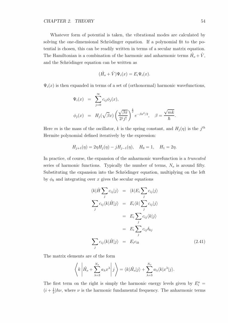
CHAPTER 2. THEORY 54
Whatever form of potential is taken, the vibrational modes are calculated by
solving the one-dimensional Schrodinger equation. If a polynomial fit to the po-
tential is chosen, this can be readily written in terms of a secular matrix equation.
The Hamiltonian is a combination of the harmonic and anharmonic terms Ho + V ,
and the Schrodinger equation can be written as
(Ho + V )Ψi(x) = EiΨi(x).
Ψi(x) is then expanded in terms of a set of (orthonormal) harmonic wavefunctions,
Ψi(x) =
∞∑j=0
cijφj(x),
φj(x) = Hj(√βx)
(√βπ
2jj!
) 12
e−βx2/2, β =
√mk
~.
Here m is the mass of the oscillator, k is the spring constant, and Hj(η) is the jth
Hermite polynomial defined iteratively by the expression:
Hj+1(η) = 2ηHj(η) − jHj−1(η), H0 = 1, H1 = 2η.
In practice, of course, the expansion of the anharmonic wavefunction is a truncated
series of harmonic functions. Typically the number of terms, No is around fifty.
Substituting the expansion into the Schrodinger equation, multiplying on the left
by φk and integrating over x gives the secular equations
〈k|H∑
j
cij|j〉 = 〈k|Ei
∑j
cij|j〉∑
j
cij〈k|H|j〉 = Ei〈k|∑
j
cij|j〉
= Ei
∑j
cij〈k|j〉
= Ei
∑j
cijδkj
∑j
cij〈k|H|j〉 = Eicik (2.41)
The matrix elements are of the form⟨k
∣∣∣∣∣Ho +
Nx∑λ=3
aλxλ
∣∣∣∣∣ j⟩
= 〈k|Ho|j〉 +
Nx∑λ=3
aλ〈k|xλ|j〉.
The first term on the right is simply the harmonic energy levels given by Eoi =
(i+ 12)hν, where ν is the harmonic fundamental frequency. The anharmonic terms
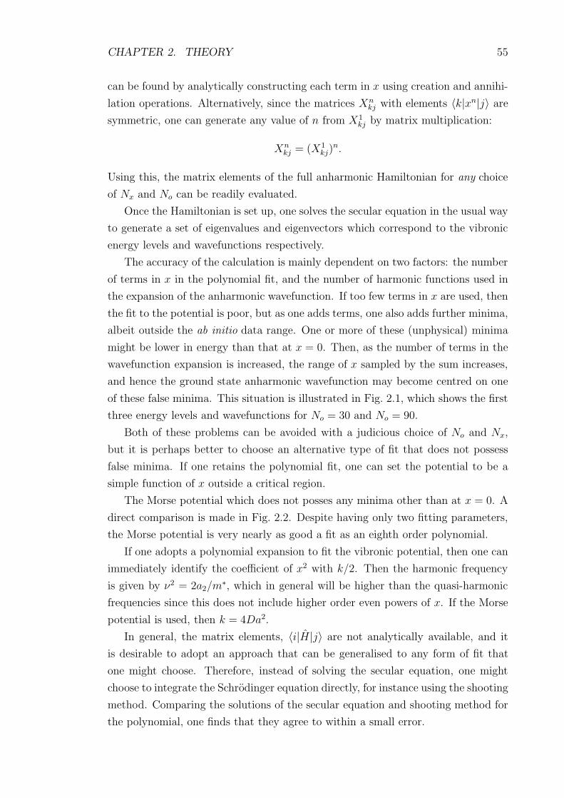
CHAPTER 2. THEORY 55
can be found by analytically constructing each term in x using creation and annihi-
lation operations. Alternatively, since the matrices Xnkj with elements 〈k|xn|j〉 are
symmetric, one can generate any value of n from X1kj by matrix multiplication:
Xnkj = (X1
kj)n.
Using this, the matrix elements of the full anharmonic Hamiltonian for any choice
of Nx and No can be readily evaluated.
Once the Hamiltonian is set up, one solves the secular equation in the usual way
to generate a set of eigenvalues and eigenvectors which correspond to the vibronic
energy levels and wavefunctions respectively.
The accuracy of the calculation is mainly dependent on two factors: the number
of terms in x in the polynomial fit, and the number of harmonic functions used in
the expansion of the anharmonic wavefunction. If too few terms in x are used, then
the fit to the potential is poor, but as one adds terms, one also adds further minima,
albeit outside the ab initio data range. One or more of these (unphysical) minima
might be lower in energy than that at x = 0. Then, as the number of terms in the
wavefunction expansion is increased, the range of x sampled by the sum increases,
and hence the ground state anharmonic wavefunction may become centred on one
of these false minima. This situation is illustrated in Fig. 2.1, which shows the first
three energy levels and wavefunctions for No = 30 and No = 90.
Both of these problems can be avoided with a judicious choice of No and Nx,
but it is perhaps better to choose an alternative type of fit that does not possess
false minima. If one retains the polynomial fit, one can set the potential to be a
simple function of x outside a critical region.
The Morse potential which does not posses any minima other than at x = 0. A
direct comparison is made in Fig. 2.2. Despite having only two fitting parameters,
the Morse potential is very nearly as good a fit as an eighth order polynomial.
If one adopts a polynomial expansion to fit the vibronic potential, then one can
immediately identify the coefficient of x2 with k/2. Then the harmonic frequency
is given by ν2 = 2a2/m∗, which in general will be higher than the quasi-harmonic
frequencies since this does not include higher order even powers of x. If the Morse
potential is used, then k = 4Da2.
In general, the matrix elements, 〈i|H|j〉 are not analytically available, and it
is desirable to adopt an approach that can be generalised to any form of fit that
one might choose. Therefore, instead of solving the secular equation, one might
choose to integrate the Schrodinger equation directly, for instance using the shooting
method. Comparing the solutions of the secular equation and shooting method for
the polynomial, one finds that they agree to within a small error.

CHAPTER 2. THEORY 56
-1.0 -0.5 0.0 0.5 1.0 1.5 2.0 2.5 3.0Displacement, x
-0.05
0.00
0.05
0.10
0.15
0.20E
nerg
y (e
V)
Ab initioFitE0
E1
E2
(a)
-1.0 -0.5 0.0 0.5 1.0 1.5 2.0 2.5 3.0Displacement, x
-0.05
0.00
0.05
0.10
0.15
0.20
Ene
rgy
(eV
)
Ab initioFitE0
E1
E2
(b)
Figure 2.1: Plots showing the solutions to the secular equations 2.41 where (a) No = 30, and (b)No = 90. The displacement, x, is in a.u., and the wavefunctions have been shifted vertically sothat each is zeroed about its energy level.

CHAPTER 2. THEORY 57
-1.0 -0.5 0.0 0.5 1.0 1.5 2.0 2.5 3.0Displacement, x
-0.05
0.00
0.05
0.10
0.15
0.20
Ene
rgy
(eV
)
Ab initioPolynomialMorse
Figure 2.2: A plot of the polynomial potential as plotted in Fig. 2.1 also showing the Morsepotential fit.
Using the above method for calculating the anharmonic vibrations, one can
examine how the calculated frequencies vary with changing values of χ or bond-
length. The effect of χ is very small: neglecting χ in the case of the CAs-H complex
in GaAs leads to a 30 cm−1 (∼1%) shift in frequency. The equilibrium bond length
cannot be altered in the calculations directly. This is simulated by the application of
a linear shift to the potential that changes the location of the minimum. Changing
the effective bond-length in this way reveals a marked sensitivity.
In fact, as highlighted in Sec. 2.15.1, bond-length is the critical quantity for the
absolute magnitude of local vibrational modes (LVMs), but differences are some-
what less sensitive. This appears to remain true for anharmonicity, as described in
detail for the CAs-H case (Sec. 6.2).
2.15.2.3 Electrical anharmonicity
The above analysis treats the mechanical anharmonicity, but there is also an an-
harmonicity in the electrical characteristics of the vibration, that is to say that the
dipole moment is not linear in x. In general, under the dipole approximation, the
integrated intensity of a local vibrational mode is proportional to
|〈Ψi |p(x)|Psij〉|2 ,
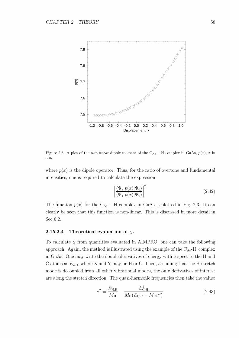
CHAPTER 2. THEORY 58
-1.0 -0.8 -0.6 -0.4 -0.2 0.0 0.2 0.4 0.6 0.8 1.0Displacement, x
7.5
7.6
7.7
7.8
7.9
p(x)
Figure 2.3: A plot of the non-linear dipole moment of the CAs − H complex in GaAs, p(x), x ina.u.
where p(x) is the dipole operator. Thus, for the ratio of overtone and fundamental
intensities, one is required to calculate the expression∣∣∣∣〈Ψ2|p(x)|Ψ0〉〈Ψ1|p(x)|Ψ0〉
∣∣∣∣2
(2.42)
The function p(x) for the CAs − H complex in GaAs is plotted in Fig. 2.3. It can
clearly be seen that this function is non-linear. This is discussed in more detail in
Sec 6.2.
2.15.2.4 Theoretical evaluation of χ.
To calculate χ from quantities evaluated in AIMPRO, one can take the following
approach. Again, the method is illustrated using the example of the CAs-H complex
in GaAs. One may write the double derivatives of energy with respect to the H and
C atoms as EX,Y where X and Y may be H or C. Then, assuming that the H-stretch
mode is decoupled from all other vibrational modes, the only derivatives of interest
are along the stretch direction. The quasi-harmonic frequencies then take the value:
ν2 =EH,H
MH
− E2C,H
MH(EC,C −MCν2). (2.43)

CHAPTER 2. THEORY 59
Substituting Eq. 2.38 with k = EH,H, one can express χ as follows:
χ =
(EH,H
EC,H
)2 1 − EC,C
EH,H
MH
MC
+MH
χMC
. (2.44)
Note, χ is only weakly dependent the hydrogen mass if the 2nd and 3rd terms in
braces in Eq. 2.44 are small. This is true when
EC,C
EH,H MC
MH.
If this were not the case, and if EC,C is large (such as if the C-back bonding is
strong) then χ can reasonably be less than unity. If the C atom was decoupled
from the rest of the lattice, then translational symmetry would require:
EH,H = EC,C = −EC,H.
Then Eq. 2.44 gives χ=1 and
ν2 = EH,H
(1
MH+
1
MC
),
as expected.
2.15.3 Effective charges
The integrated intensity, I of a vibrational mode is related to the induced dipole
moment through the expression [57]:
I =2π2ρ
ncmη2, (2.45)
η2 =∑
k
m
(∂Mx
∂Qki
)2
,
where ρ is the concentration of the impurity, n is the refractive index, c is the
speed of light, m is the impurity mass, η is the effective charge of the LVM, Mx
is the induced dipole in the direction of the applied electric field (x), Qi is the
normal coordinate of the ith normal mode, and the sum is over any degeneracy in
the normal modes.
The induced dipole M can be evaluated in the cluster formalism using the
expression
M =∑
a
ZaRa −∫
rn(r)dr,
where the atoms are displaced according to the normal co-ordinate, that is to say
byQiu
ila√m.

CHAPTER 2. THEORY 60
If the defects are randomly oriented, then it is necessary to average over the
different orientations, so that, for example, the effective charge on a non-degenerate
mode at a C3v centre is given by [58]:
η2 =m
3
∑l
(∂Ml
∂Q
)2
.
Note however, defects are not always randomly oriented. For example the (CAs)2−H
centre in GaAs is preferentially aligned along one 〈110〉 direction (see Chapter 6).
Using this method, the effective charge for all the modes of a given centre can
be calculated. Suppose that only one mode is observed experimentally. Then, if
one of the modes possesses a value of η greater than the others, this is a strong
indication that this is the one that is experimentally observed.
2.16 Multiplets
The derivation of DFT is strictly applicable only to ground state systems, for which
the theory predicts properties with quantitative accuracy. However, problems arise
when several degenerate orbitals are only partially filled, such as in the case of high
symmetry defects. An example in diamond of such as a (C3v) defect is the vacancy
bordered by a single nitrogen atom (see Chapter 4). This type of problem involves
multiplet structures and therefore should strictly be beyond the theory. However,
von Barth [59] developed a method for obtaining approximate multiplet energies
using DFT.
Under this approach the density functional energy is related to a specific de-
terminental wavefunction, the contents of which are in turn dictated by the choice
of occupancy of the KS levels. The energies of different multiplets can therefore
be generated by a judicious choice of these occupancies. Each determinant can be
written as a linear combination of multiplets, |D〉 =∑
a ca|Ma〉. Operating on each
determinant with the Hamiltonian and finding the expectation gives:
〈D|H|D〉 = E =∑
a
|ca|2〈Ma|H|Ma〉.
Given sufficient independent determinants, one can then deduce values for the mul-
tiplet energies, such as in the neutral vacancy-nitrogen complex in diamond. How-
ever, this is not always possible, as in the case of the neutral vacancy in diamond.
2.17 Electronic transitions
Experimentally, for a particular electronic transition the symmetry of the ground
and excited states, the zero-phonon energy, and the radiative lifetime may be known.

CHAPTER 2. THEORY 61
Of all of these terms, all but the first is related to an excited state of the system.
Fortunately, as described above, we can get around this problem in a number of
favourable cases where multiplet structures can be found. Thus, but occupying
the orbitals appropriately, we can estimate the energy of the excited state, and
hence the energy of the optical transition between this state and the ground state.
Alternatively, theory due to Slater [16] allows one to estimate the transition energy
with a single calculation.
2.17.1 Transition states
The problem is to calculate the energy of a transition between electronic states with
energy Eλ and Eµ. According to the Slater transition state method, the transition
energy is given by the difference between the KS levels, Eµ − Eλ when half an
electron is promoted from the lower to the higher orbital, i.e. both Eλ and Eµ are
half filled. Note that this transition energy is not the same as the zero-phonon
energy, and differs from it by the relaxation energy. This method has been used
successfully in a number of cases in diamond [60], and gives energies very similar
to the energy difference between the ground and excited multiplets.
2.17.2 Radiative lifetimes
The rate at which electrical dipole transitions occur between states λ and µ can be
estimated using the following relationship [61]:
1
τλµ=
4nω3
3c3~
e2
4πεo|rλµ|2 (2.46)
rλµ =∑
s
〈ψλ(r, s)|r|ψµ(r, s)〉, . (2.47)
where n the refractive index, e the electron charge, c the speed of light and ω the
transition frequency.
Within AIMPRO this integral is calculated for the pseudo-wavefunctions of the
KS-levels, which is not strictly correct since the wavefunctions are zero near the
atomic nuclei. Also, due to the cubic dependence of the transition rate on the
frequency, the calculations are very sensitive to errors in ω. Despite these short
comings, these calculations have given correct order of magnitude estimates in the
case of vacancy-impurity defects in diamond [60].
2.18 Clusters
It is important to select an appropriate basis set and cluster to treat a particular
defect.

CHAPTER 2. THEORY 62
In general, the wavefunction basis for each atom is made up of a number of
atom centred s- and p-Gaussian orbitals. For transition elements there are further
d-Gaussian orbitals, and for the lanthanides f -Gaussian orbitals. GaAs, Si and Ge
also require d-orbital character in the basis set, and this can be achieved either by
explicitly having atom centred d-Gaussian orbitals or, more simply, by adding bond
centred Gaussians.
The wavefunction basis functions are as introduced in Sec. 2.12,
(x− Rix)n1(y −Riy)
n2(z − Riz)n3e−ai(r−Ri)
2
, ni ∈ N .
ni = 0, i = 1, 2, 3 gives one the s-Gaussians, n1 = 1, ni = 0, i = 2, 3 generates the
p-Gaussian functions, and the d- and f -Gaussians can be generated if∑
i ni = 2
and∑
i ni = 3 respectively. The complete wavefunction basis is then made up of a
linear superposition of the atom- and bond-centred orbitals.
The exponents, ai, for a particular atom are found by minimising the total
energy of the pseudo-atom. This procedure also generates a set of coefficients, cλi
from Eq. 2.22. Then these coefficients can be used in the fixed linear combination
with different exponents to form a ‘minimal basis’. If the coefficients multiplying the
orbitals are treated as variational parameters, the basis is termed ‘big’. In a large
cluster one usually has the central atoms of the defect and the nearest neighbours
in big basis and the remaining, more remote atoms in minimal basis.
As described above, the charge density is also expanded in terms of basis func-
tions (Eq. 2.25 and pure Gaussians), both at atom- and bond-centres. In this case
the optimal basis is established by maximising the estimated Hartree energy EH,
as described above in Sec. 2.12.1.
Typically, for a sp bonding material such as C or Si, the basis is made up of
3-4 sets of Gaussians in the wavefunction expansion and 4-5 charge density fitting
functions, although for some problems a bigger basis is required, with, for instance,
eight sets of wavefunction Gaussians, and eight charge density fitting functions. For
transition metal elements, the number of charge density fitting functions increases
dramatically since the atomic charge density increases near the origin as r4, and
is poorly represented by the functions in Eq. 2.25. In applying the basis selection
to a cluster, it is important that the arrangement of big/minimal basis atoms and
bond-centres reflects the symmetry of the defect.
One consequence of using a Gaussian basis set is that increasing the number
of functions can lead to an ‘over-complete’ basis, which results in an instability
in the Choleski decomposition of the overlap matrix. Therefore, in contrast to
the calculations using a plane-wave basis, one cannot strictly converge the total
energy. However, in practice it is usual to be examining energy differences, such as

CHAPTER 2. THEORY 63
in the relative stabilities of defect structures or the excitation energy of an electron
from one multiplet to another, and these energies are usually well described using
AIMPRO.
The clusters are terminated with hydrogen, with the X-H bonds oriented along
the bulk bond direction. The cluster itself takes two main forms. The first is
atom-centred surrounded by concentric shells of bulk atoms. This cluster therefore
possesses a tetrahedral symmetry. For the III-V’s, this means that there is an
excess of either the group-III or group-V atom type, and consequentially the neutral
cluster would have the incorrect number of bonding electrons. For all of the bonding
orbitals to be filled, the neutral charge state is modelled by charging the cluster by
the difference in the number of, group-III and group-V atoms. For example, a Ga
centred cluster Ga19As16H36 would be charged by 3e.
The second type of cluster is bond centred, which avoids the charging problem
encountered in the atom centred III-V cluster as these clusters contain the same
number of group-III and group-V atoms (by symmetry). This type of cluster is
referred to as stoichiometric, and possesses trigonal symmetry. One disadvantage
of using stoichiometric clusters for III-V compound semiconductors is that they
possess an inherent dipole. Consequentially the central bond is longer than the six
equivalent back bonds. However, for most III-V materials all bonds are reproduced
to within 3% of the experimental value.
It is well known that DFT underestimates the band gaps of semiconductors,
and band gaps in clusters are overestimated due to the confining nature of the H-
termination. In the case of diamond, these effects conspire to give approximately
the correct values. Fig. 2.4 shows how the band gap, as estimated by the difference
in the energies of the highest occupied and lowest unoccupied KS-eigenvalues. For
Si, Ge, and GaAs, there is a clear decrease in the band-gap with increasing cluster
size, as expected. All but diamond compare rather badly with the experimental
values: 5.5, 1.17, 0.75, and 1.42 eV for diamond, Si, Ge, and GaAs respectively.
The overestimation of band gaps can be corrected by applying the so-called
scissors operator:
∆(r, r′) = V∑λ′ψλ′(r)ψλ′(r′) for λ′ unoccupied.
∆ can also be defined in terms of the occupied levels,
∆(r, r′) = V∑ij
(δi,j − bij)φi(r − Ri)φj(r′ − Rj),
and it is this form of the scissors operator that is used in AIMPRO. This is simply
added to the Hamiltonian and shifts the unoccupied states of the cluster containing

CHAPTER 2. THEORY 64
71 131 297Number of atoms
2.0
3.0
4.0
5.0
6.0
Ban
d G
ap, e
V
DiamondSiliconGermaniumGaAsGaAs
Figure 2.4: A graph showing the dependence on cluster size of the band-gap for diamond, Si,Ge, and GaAs. The group-IV materials clusters are made up as follows: X35H36, X71H60, andX181H116. There are two possible arrangements of each GaAs cluster - Ga centred and As centred.The three clusters are X19Y16H36, X31Y40H60, and X89Y92H116. In the graph, ×’s indicate Gacentred clusters and ©’s As centred clusters. (cf. experimental values of the band-gap: 5.5, 1.17,0.75, and 1.42 eV for diamond, Si, Ge, and GaAs respectively.)
no defect upwards by a quantity V . V is chosen such that the ‘pure’ cluster possesses
the experimental band-gap. The scissors operator is not often employed but has
been used in the case of gold and gold-hydrogen centres in Si.
2.19 Summary
In this chapter, I have tried to give a relatively detailed description of the road to
the methods used in AIMPRO. I have also included a description of a couple of
rival methods, namely Hartree-Fock and the parameterised methods of CNDO.
A number of sections are referred to regularly in the applications chapters,
and are of a technical nature. These include the methods used for calculations
of transition energies and rates, vibrational modes and other observables, as well
the basis functions used to model each atom.

Chapter 3
Experimental techniques
‘An expert is someone who knows some of the worst mistakes that can
be made in his subject and how to avoid them.’
- Werner Heisenberg
3.1 Introduction
A range of experimental methods have been successfully employed in the study of
defects in semiconductors and a number of these techniques (such as the frequencies
of localised vibrational mode spectroscopy and approximately the transition energy
in photoluminescence) measure quantities that are directly calculable using AIM-
PRO. Some other aspects of experimental procedure, such as uniaxial stress, are
less readily simulated directly, but still provide essential information such as defect
symmetry to the theorist.
Data on a specific defect derived from a single experiment or even single type of
experiment often proves insufficient for an unequivocal assignment to a particular
atomic and electronic structure. It is necessary to combine and correlate data from
different types of experiments, such as the optical and magnetic measurements,
which has proved effective in the case of the vacancy-nitrogen complex in diamond.
In this chapter the main experimental techniques referenced in later chapters
are outlined. Although it is not possible to examine the technicalities of each
method, the scope and accuracy is discussed in general terms. The methods covered
are: localised vibrational mode spectroscopy (especially in reference to hydrogen-
related centres); electron paramagnetic resonance; photoluminescence and related
techniques; and finally deep level transient spectroscopy.
65

CHAPTER 3. EXPERIMENTAL TECHNIQUES 66
3.2 Localised vibrational mode spectroscopy
Localised vibrational mode spectroscopy (LVMS) encompasses a range of techniques
that measure the frequency of atomic vibrations, both bulk and those originating
from defects. The two main methods are infra-red (IR) absorption and Raman
scattering and since the selection rules for the two processes are different they
can provide complementary information. As an introduction, I shall begin with a
description of the vibrational properties of a crystal.
Diamond and zinc blende structures are comprised of two interlocking face-
centred cubic lattices. These crystal structures possess three optical and three
acoustic phonon bands, however, the physics can be understood by simplifying this
problem to one-dimension. In 1-D the phonon-dispersion possesses only one acoustic
and one optical branch [62]:
ω2(q) =k
m∗ ± k
√1
(m∗)2− 4 sin2(qa)
m1m2. (3.1)
Here k is the force constant, a is the inter atomic separation, m1 & m2 (m1 ≥ m2)
are the atomic masses and 1/m∗ = 1/m1 + 1/m2. The ± distinguishes between the
acoustic (-) and optic (+) branches. Fig. 3.1 shows Eq. 3.1 in graphical form for a
compound structure with the maximum frequency, ωmax = ω(q = 0) =√
(2k/m∗).
Also shown is the gap between the optical and acoustic branches at the zone bound-
ary (q = ±π/2a) which arises from the difference in basis atom mass and therefore
is not present in the elemental semiconductors. The frequencies at the zone bound-
ary are ωa =√
(2k/m1) and ωo =√
(2k/m2) for the acoustic and optic branches
respectively.
3.2.1 Infra-red absorption
IR-absorption is particularly important for the characterisation of light impurities,
especially hydrogen. Only the basic principles and points relevant to the present
work are covered in this section. For a more complete description see Ref. [63].
For absorption in a pure crystal the crystal momentum and the energy must be
conserved. Since the momentum associated with a photon is rather small in the case
of atomic vibrations, this means that in one-phonon processes, absorption can only
occur close to q = 0. Multi-phonon processes can occur provided that the sum of the
momenta is close to zero. The absorption coefficient (i.e. the strength of absorption)
is proportional to the dipole matrix element (Sec. 2.15.3), and since there is no
induced dipole moment under the bulk normal modes of elemental semiconductors,
there is no first order absorption. However, in compound semiconductors there is

CHAPTER 3. EXPERIMENTAL TECHNIQUES 67
0-π/2a π/2aWavevector, q
ωmax
Fre
quen
cy, ω
L
ωa=(k/m1)1/2
ωo=(k/m2)1/2
Gap
Gap
Gap
Gap
Gap
Gap
Gap
Gap
Gap
Gap
Figure 3.1: The one-dimension phonon-dispersion for a material with zinc blende like structure.
a large induced dipole, and thus strong absorption around ωmax. This absorption
band is known as the ‘Reststrahl band’.
In principle, absorption can occur in processes involving any number of phonons.
However, as the number increases, the probability of such a process occurring de-
creases rapidly, and in practice only one- and two-phonon processes are important.
The frequency range ωmax → 2ωmax is where many defect related features of interest
lie1, and therefore it is essential that the bulk absorption in this range is minimised.
Fortunately, this can be achieved by cooling samples to T < 77 K.
Impurities introduce local changes in symmetry and therefore break the absorp-
tion selection rules. In general, a prerequisite for IR-absorption is the presence of
an induced dipole moment. When the frequency of an impurity vibration is far
from lattice mode frequencies, the vibration cannot propagate through the sample,
and such a mode is termed a localised vibrational mode (LVM). If the impurity
mass is large, i.e. mimp > m1, the impurity will possess normal modes that lie in
the bulk absorption bands, which may be observed as resonances, such as those of
nitrogen in diamond. Resonant mode absorption peaks tend to be broad, making
them difficult to observe unless the concentration of the impurity is very high2.
However, the presence of heavy impurities can sometimes be inferred from modes
1For example, GaAs possess ωmax ≈ 285 cm−1 [64], and SiGa:GaAs has a local mode at384 cm−1.
2In the case of diamond, it is known that nitrogen may be present in concentrations as high asparts per thousand.

CHAPTER 3. EXPERIMENTAL TECHNIQUES 68
of light impurities (such as hydrogen) when they are attached to them.
As noted above, there is a gap in the density of phonon modes between the
acoustic branch maximum and optical branch minimum. Impurity modes at be-
tween these frequencies may be detected. For example, As at an P site in GaP
exhibits such a local mode [65], where the increase in mass (from 31 to 75 amu)
lowers a mode into the gap. Other examples of gap-modes in GaP are BGa and SiGa.
Note, both B and Si also possess higher frequency modes. The phonon density of
states may possess other local minima that allow observation of local modes, such
as the 156 cm−1 mode of BGa in GaP.
Despite the fortuitous location of some LVMs for frequencies < ωmax, infrared-
absorption spectroscopy is usually employed in the detection of higher frequency
modes which invariably arise from impurities with a low mass3. These modes can be
represented by Eqs. 2.38 and 2.39 (see Sec. 2.15.2). All terms in Eq. 2.45 are known
except for the defect concentration (ρ) and the ‘effective charge’ of the vibration
(η). To determine these, experimental calibrations must be made by estimating the
concentration using an alternative method, such as secondary ion mass spectroscopy
(SIMS)4, but this procedure is complicated and destructive. Note, this calibration
must be performed for each defect.
The symmetry of a centre can be established by applying uniaxial stress in (say)
the [100], [011], and [111] directions and observing the absorption peaks. The way
in which the peaks split with stress indicates the symmetry. This is called stress
dichroism, and can be applied to most spectroscopic techniques. As an example,
one can consider the case of the fully hydrogenated vacancy in silicon [13]. Uniaxial
stress shows here that the (threefold degenerate) 2222 cm−1 band splits into two
components under a 〈111〉 applied stress. In the 〈100〉, 〈110〉 and non-symmetric
directions, the band is split into three. This is indicative of a cubic symmetry,
e.g. Td. In fact just knowing that the mode is threefold degenerate is sufficient to
identify this symmetry.
The application of uniaxial stress can also be used to gain information about the
energy required to reorient a defect between equivalent configurations. This process
is known as stress induced alignment and is carried out as follows. As an illustration
the case of the CAs-H centre in GaAs is used [67]. First, uniaxial stress is applied
in one of the 〈111〉 (say [111]) directions at a (relatively5) high temperature. The
stress makes the four alignments of the CAs-H centre inequivalent, and since the
3relative to m2.4SIMS involves the bombardment of the sample with primary ions and the detection of sec-
ondary ions sputtered from the sample surface. This procedure can be used to detect the presenceof dopants, and their distribution with depth. For a full explanation see Ref. [66].
5This temperature must be greater than the temperature at which the defect can reorient.

CHAPTER 3. EXPERIMENTAL TECHNIQUES 69
centre can reorient, the lowest energy directions will be preferentially occupied. In
the CAs-H case the [111], [111] and [111] directions are equivalent. The sample is
then rapidly cooled while the stress is maintained, and the alignment is frozen in.
If an absorption experiment is then performed, in the different 〈111〉 directions the
CAs-H absorption will be different. One can then anneal the sample at increasing
temperatures. The absorption will follow the relation [68]
n(t) − no = [n(0) − no]e−t/τ ,
where no is the equilibrium value of the concentration of the defect oriented along
one 〈111〉 direction, which at a time t is n(t). The reorientation time constant, τ is
given by the expression1
τ= νoe
−U/kBT ,
with νo being an attempt frequency and U the barrier to reorientation. For CAs-H in
GaAs, U = 0.63 eV.
To establish the chemical constituents of a defect one can examine the fine
structure in the absorption bands due to different isotopes. For example, SiGa :
GaAs gives rise to bands at 384, 379, and 373 cm−1 with intensities that correlate
to the abundances of 28Si, 29Si, and 30Si. For the complex of H with CAs in GaAs,
there are modes at 2635 and 2628 cm−1 for 12C and 13C respectively. Thus, hydrogen
is can be used as a probe to identify impurities to which it binds. This is especially
useful for the heavy impurities that cannot be directly observed by IR-absorption,
such as the H-passivation of Zn acceptors in GaAs [69].
Isotopic data can also provide information about symmetry. For an impurity at
an As site, isotopic shifts will be seen due to 69Ga and 71Ga. The number of equiva-
lent Ga atoms can be deduced from the relative intensities of the mixed isotope lines,
and hence some information regarding the local symmetry. For a sufficiently small
change in mass, the isotopic shift is given approximately (by assuming Eq. 2.38) as
2δν
ν=δm∗
m∗ .
Whether or not the charge state induces a change in the LVM is dependent
on the position of the defect state in the gap. If the level is shallow, then the
associated wavefunction is dispersed over a large region of space. Then, occupying
or not occupying this state will have little effect on the local geometry of the defect,
and hence the LVMs. However, if the gap-level is deep, this correspond to the
wavefunction being more localised, and the occupancy is more likely to affect the
structure.
The breadth of an absorption peak is dependent on a number of factors: the
lifetime of the excited vibronic state, the strains inherent in the sample, and the

CHAPTER 3. EXPERIMENTAL TECHNIQUES 70
isotopic shifts. The lifetime can be increased by lowering the temperature, and
the strains can be reduced by improving the sample quality. Typically, the full
width at half peak is 1 cm−1 or less at 77K, and Fourier transform IR-spectroscopic
techniques lead to a precision in the frequency of as good as 0.01 cm−1.
The concentration required for detectability is dependent on the quality of the
sample, the sample dimensions and the induced dipole of the LVM. However, typi-
cally a concentration of at least ρ ∼ 1015 cm−3 is required for a 1 mm thick sample.
In favourable conditions this minimum may be reduced: for sharp peaks, concen-
trations as low as 1013 cm−3 can be detected.
Due to the IR-absorption selection rules, some LVMs are not IR-active (i.e.
the induced dipole is zero by symmetry). However, the scattering selection rules
are different from those for absorption, and one can combine IR-absorption and
Raman spectra to provide a more complete picture of a defect centre. For example
the 739 cm−1 mode of the CAs-H complex in GaAs is not seen in IR-absorption
(despite being IR-active by symmetry) but is seen in Raman [70] (see Chapter 6).
3.2.2 Raman scattering
If one illuminates a crystal with monochromatic light (frequency ωo), the resulting
scattered radiation spectrum includes a strong line at ωo, and weaker lines at ωo ±ωj(q), where ωj(q) are the optical phonon frequencies. The central peak is due to
elastically or Rayleigh scattered photons, whereas those at ωo−ωj(q) and ωo +ωj(q)
are inelastic or Raman scattered and termed Stokes and anti-Stokes lines. This can
be viewed more quantatively as follows.
One can write down the (time dependent) induced dipole as
M(t) =∑
eiri(t) (3.2)
If the incident radiation possess an oscillatory electric field given by E = Eo cosωot,
then the induced dipole M can be expressed as a series in E:
M = αE +1
2βE2 + higher terms (3.3)
α is the electronic polarisability of the system, and β is a third rank tensor termed
the hyper-polarisability. β is responsible for the so-called hyper-Raman effect which
is beyond the scope of this chapter.
α is dependent on the charge distribution in the system and thus, in general,
will vary with atomic vibrations. One can expand α as a Taylor series:
α = αo +
(∂α
∂Q
)Q+
1
2
(∂2α
∂Q2
)Q2 + ... (3.4)

CHAPTER 3. EXPERIMENTAL TECHNIQUES 71
where Q is the normal co-ordinate of the vibration. If one writes Q = Qo cosωst,
where ωs is the characteristic frequency of the mode, one can re-write the induced
dipole to first order in polarisability as:
M(t) = a cosωot+ b [cos(ωo − ωs)t+ cos(ωo + ωs)t] (3.5)
a = αoEo, b =1
2
(∂α
∂Q
)QoEo.
Here, the first term is Rayleigh peak with frequency ωo, and the remaining terms
are the Stokes and anti-Stokes shifted peaks.
This classically based theory then can be used to predict the relative intensi-
ties of the Stokes and anti-Stokes peaks, but does so incorrectly. The intensity is
proportional to ∣∣∣∣d2M
dt2
∣∣∣∣2
,
which results in a ratio intensities of
IStokes
IAnti−Stokes=
(ωo − ωs)4
(ωo + ωs)4.
Clearly, this quotient is less than unity indicating that the anti-Stokes peak is more
intense, whereas experimentally the Stokes peak is the most intense.
In order to correct this error, one needs to perform a quantum mechanical deriva-
tion of the Raman effect. This results in an intensity ratio of
IStokes
IAnti−Stokes
=(ωo − ωs)
4
(ωo + ωs)4e~ωs/kBT ,
which correctly gives a ratio > 1.
Whether or not a vibrational mode is Raman active is dependent on the polar-
isability tensor, αρσ. The induced dipole to first order in E is written: Mx
My
Mz
=
αxx αxy αxz
αyx αyy αyz
αzx αzy αzz
Ex
Ey
Ez
(3.6)
Since αρσ is symmetric, one can perform a transformation (x, y, z) → (x′, y′, z′),
that will diagonalise this set of equations: M ′
x′
M ′y′
M ′z′
=
α′
x′x′ 0 00 α′
y′y′ 00 0 α′
z′z′
E ′
x′
E ′y′
E ′z′
. (3.7)
(x′, y′, z′) are termed the principle axes of the equilibrium structure, and in general,
one can always choose a set of co-ordinates that give a diagonal polarisability tensor.
CHAPTER 3. EXPERIMENTAL TECHNIQUES 72
For convenience the primes are dropped, and equilibrium values denoted by the
superscript o: αo
xx 0 00 αo
yy 00 0 αo
zz
When the system is perturbed under the motion of a normal mode, there is a change
in the polarisability. One can write down the polarisability for the perturbed system
in terms of a Taylor expansion:
αρσ = αoρσ +
∑s
αρσ,sQs +1
2
∑s1,s2
αρσ,s1,s2Qs1Qs2 + ... (3.8)
where the notation
αρσ,s =∂αρσ
∂s.
To first order, the change in polarisability is αρσ,sQs, which is itself a tensor
quantity. This leads to a generalised expression of the form of Eq. 3.5
M(t) = aρ cosωot+∑
s
bs,ρ [cos(ωo − ωs)t+ cos(ωo + ωs)t] (3.9)
aρ =∑
σ
αoρσEoσ,
bsρ =1
2Qo
∑σ
(∂αρσ
∂Qs
)Eoσ
As before, the first term is Rayleigh scattering, and the remaining two terms Stokes
and anti-Stokes. The latter are dependent on the terms αρσ,s. Therefore, in order for
Raman scattering to occur it is necessary that bsρ 6= 0. In other words, the change
in polarisability with the normal mode must, in some direction, be non-zero.
Despite the difficulty in performing Raman scattering experiments to charac-
terise defects in solids, the fact that the selection rules mean that modes that are
IR-inactive may be seen in Raman makes the technique very useful. Note, it is not
true that all IR-active modes are Raman-inactive or visa versa.
3.2.3 Summary
In summary, LVMS can be used to identify the vibrational frequencies of bulk
modes and a range of defects, with particular emphasis on the lighter elements such
as hydrogen. Uniaxial stress and isotopic data can be used to determine a detailed
picture of the defect responsible for a particular LVM. Typically, however, a large
concentration of the defect is required. Modes that do not possess an induced dipole
moment are not visible under IR, but may be Raman active and visa versa.

CHAPTER 3. EXPERIMENTAL TECHNIQUES 73
3.3 Electron paramagnetic resonance
Where there is an excess of one electronic spin at a defect site (i.e. the effective spin
S is non-zero) the centre possesses a net magnetic dipole moment and, provided that
they do not interact, such centres are termed paramagnetic. An applied magnetic
field, Bo, will align these unpaired spins which will possess discrete energies Ei. If
a sample is subsequently exposed to electromagnetic radiation with frequency ν,
such that hν is equal to the separation between E0 and E1, absorption will occur.
This phenomenon is termed electron paramagnetic resonance (EPR), also known
as electron spin resonance (ESR). The discussion presented in this section is not
intended to be exhaustive, and further details may be found in Refs. [71] and [72].
EPR can be used to find a range of qualitative and quantitative properties of
defects. These include symmetry, nuclear spin of the defect atom, nuclear spin of
neighbouring atoms and the localisation of the wavefunction associated with the
unpaired electron.
3.3.1 Dipolar magnetic moment
One needs to begin by considering an electron in a magnetic field: an electron in a
magnetic field will move in a circular path. This is termed the cyclotron orbit. An
electron with an orbital angular frequency ω gives rise to a current
I =−eω2π
= −eν,which in turn gives rise to a magnetic dipole moment, µo. The electron angular
momentum, l, in units of ~, is given by meωr2, where r is the radius of the orbit
and me is the electron rest mass, and hence the dipole magnetic moment is given
by
µo = −goµBl,
where the constant go = 1 and
µB =e~
2me
is the Bohr magneton.
The dipole magnetic moment is aligned in the direction normal to the plane of
the orbit. Next, one must include the contribution due to the intrinsic electron spin
angular momentum, s. This is given by
µs = −gsµBs,
where gs is the electron spin g-factor6 Finally, one can write down a total magnetic
moment, µ = µo + µs.6gs is 2.0023 for the free electron.

CHAPTER 3. EXPERIMENTAL TECHNIQUES 74
Let us first consider the simplest case: the unpaired electron is in an orbitally
non-degenerate state. The electron spin is limited to ±1/2 and the interaction
energy of the external field with the unpaired electron is given by −µs.B = gsµBs.B
which is the electronic Zeeman energy. If we choose the magnetic field to be aligned
along z, this simplifies to
Eel−Zeeman = gsµBBoms, ms = ±1
2, (3.10)
since the eigenvalues of sz are ±12. Then, the condition for resonance is that the
incident radiation has the same energy as the difference in the Zeeman energies, i.e.
hν = ∆Eel−Zeeman = gsµBBo. For an applied magnetic field of around a third of one
Tesla, this gives frequencies in the microwave band.
3.3.2 Absorption and derivative outputs
In practice the incident frequency is constant and the magnetic field is varied, giving
a graph of absorption against field. However, the absorption is often extremely weak
and superimposed on a large, slowly changing background. A modulated technique
is needed to enhance the signal 7.
This uses a second, alternating magnetic field applied in the direction of the
static Bo at 100 kHz with an amplitude somewhat less than the absorption line-
width. The (weak) output signal is usually further enhanced as follows: the detector
output is put into a lock-in amplifier which multiplies the signal by a weighting with
the same frequency as the oscillating field. The amplifier also integrates the signal
over many periods. When Bo is in resonance this produces a signal (provided that
the modulated field is sufficiently small) with an amplitude proportional to the
gradient of the absorption peak. This is illustrated in Fig. 3.2. The figure shows
the derivative plot with an amplitude W , and a line-width defined as the separation
between the two peaks ∆Bo. The integrated intensity is then given by W × ∆Bo
which is proportional to the concentration of spins. To convert this into an actual
concentration, as with IR-absorption the signal must be calibrated using a sample
where the spin concentration is known.
3.3.3 Nuclear Zeeman effect
Just as an electronic spin gives rise to a dipolar magnetic moment, so does a nuclear
spin. The nuclear Zeeman energy can be written down in exactly the same way as
7There is an alternative method where the signals are measured in ‘dispersion mode’ and theoutput is like an absorption. This allows the use of higher microwave powers for the detection ofweak signals, but lacks the resolution of the modulated scheme.

CHAPTER 3. EXPERIMENTAL TECHNIQUES 75
source detector
sample
mod.
ref.
ref.
PSD
dBB
B
Abs
orpt
ion
B∆
(MA)
Der
iviti
ve W
B∆ o
Magnetic Field,
Figure 3.2: On the left is shown how the experiment is set up such that the modulation is usedas a reference to enhance the modulated output using a phase sensitive detector (PSD). On theright is shown a schematic of the absorption and absorption derivative EPR spectra. The ‘wave’indicated by ‘(MA)’ shows the modulated absorption produced by the modulated magnetic field,∆B.
the electronic Zeeman energy:
Enuc−Zeeman = gNµNBomI , mN = ±1
2
where µN = e~/2mp is the nuclear magneton, and the (proton) nuclear g-factor is
gN = 5.5854. mp is the rest mass of a proton. Note, gN is dependent on the ac-
tual nucleus under study. The nuclear magneton is some three orders of magnitude
smaller than the Bohr magneton, and hence the nuclear Zeeman splittings corre-
spond to much higher frequency resonances (O(10 MHz)). The nuclear Zeeman
effect gives rise to an extra set of peaks split off from the main peaks.
In the same way as a resonance in the microwave frequency range is sought in
EPR, a radio frequency resonance can be sought for the nuclear Zeeman splittings.
The simultaneous resonance in terms of both the electronic and nuclear spins is
termed electron nuclear double resonance (ENDOR). The interpretation of ENDOR
data is even more complicated than that of EPR.
3.3.4 The hyperfine interaction
The hyperfine interaction is due to the magnetic coupling between the nuclear and
electronic spins:
Hhyp = gsgNµBµN
[s.I
r3− 3(s.r)(I.r)
r5
](3.11)
Once again, aligning the applied field along z only the z-components are retained,
and the hyperfine interaction can be written:
Hhyp =1
r3gsgNµBµNszIz(1 − 3 cos2 θ), (3.12)

CHAPTER 3. EXPERIMENTAL TECHNIQUES 76
where θ is the angle between r and z.
Typically, the hyperfine energy is of the order of 100 times smaller than the
electronic Zeeman energy, and thus can be considered as a perturbation. Hhyp
in the above form is singular at r = 0, which must be corrected for the finite
probability of finding the electron in the nuclear core. This correction is called the
Fermi contact term and is incorporated in the central hyperfine term:
Hcentral−hyp = gsgNµBµN8π
3|ψ(0)|2s.I, (3.13)
Here, ψ(r) is the wavefunction associated with the unpaired electron. Reducing
everything to the z-direction, one can write Eq. 3.13 as
Hcentral−hyp = AmsmI ,
where A is the central hyperfine parameter. This term is typically comparable to
the hyperfine energy. In general, the nuclear spin I may take any half-integer value,
and hence give rise to (2I + 1) values of resonant field.
3.3.5 Spin orbit coupling
The spin-orbit interaction leads to an anisotropy in the electronic g-factor, and
this can be used to examine the symmetry of the defect. The spin-orbit interac-
tion is characterised by the Hamiltonian term HS−O = ηl.s, where deviations from
isotropy are determined by the sign and magnitude of η/(E1−E0). Here, the energy
subscripts 0 and 1 refer to the ground and excited electronic Zeeman split levels
respectively. The direction of the applied field is varied, and the measured g-factor
obeys the relation
g2 = g2‖ cos2 θ + g2
⊥ sin2 θ,
where θ here refers to the angle between the direction or the spin and the applied
field.
3.3.6 High spin centres
In some cases the electronic spin of the centre is S > 12, in which case there will be
(2S + 1) electronic Zeeman levels, E0, E1, ..., E(2S). For example, the S = 1, nega-
tively charged vacancy-nitrogen complex in diamond would possess three Zeeman
split energy levels.
3.3.7 Low symmetry defects
The expressions thus far have been applicable specifically to a system with Td sym-
metry. In general one should include terms in the total energy for lower symmetries.

CHAPTER 3. EXPERIMENTAL TECHNIQUES 77
For systems with lower than axial symmetry system there are the extra terms:
D
[S2
x − S(S + 1)
3
]+ E
(S2
x − S2y
).
Then for axial symmetry E = 0, and for tetrahedral systems, D = 0, to return to
the original expression. These additional energy terms give rise to an additional 2S
lines in the absorption, which is referred to as fine structure.
To disentangle the peaks due to the fine and hyperfine terms, one can use the
fact that the hyperfine interaction is independent of the incident radiation frequency
whereas the fine structure is not. Then, by comparison of spectra of different
microwave cavity dimensions, one can identify the hyperfine and fine structure.
There are a number of other effects that are not mentioned here in detail. These
include the so called super-hyperfine interaction, which relates to nuclear spins in
atoms adjacent to the defect and high order interactions such as the magnetic
quadrupole effect.
EPR can detect, in general, lower concentrations of defect centres than infra-
red absorption, but the actual resolution is dependent on the line width of the
absorption. Typically, concentrations from greater than 1012 cm−3 can be detected.
3.3.8 Optical detection of magnetic resonance
An allied method to EPR is optical detection of magnetic resonance (ODMR). Here
the microwave transitions are induced in an optically excited state of the centre and
detected through a change in the luminescence intensity or luminescence polarisabil-
ity. An ODMR spectrum consists of variation in luminescence with magnetic field,
and thus the detection is much more sensitive than EPR since a photon detector is
much more sensitive than a microwave detector.
3.3.9 Summary
In summary, EPR and related techniques can provide a great deal of information
about defects with unpaired electrons, such as the localisation of the wavefunction
associated with the unpaired spin, and the symmetry of the defect. However, the
deconvolution of the various terms in the spin Hamiltonian is not simple and a
number of approximations are made, such as treating the unpaired electronic and
nuclear spins as points when estimating their separations. This has been done in
some cases by splitting the hyperfine interaction into isotropic (a) and anisotropic
(b) terms. Then assuming a the hyperfine interaction is essentially a dipole-dipole
interaction the separation is estimated from the expression: b = gµBgNµN/r3. For
more details, see, for example, Ref. [73].

CHAPTER 3. EXPERIMENTAL TECHNIQUES 78
3.4 Photoluminescence
Photoluminescence (PL) is one of many optical techniques that have been widely
employed in the characterisation of semiconductors. Other techniques closely re-
lated to PL are cathodoluminescence (CL) where the incident radiation takes the
form of electrons rather than photons, photoluminescence excitation (PLE) and
absorption, all of which shall be touched upon in this section.
During PL, samples are exposed to illumination with light of a frequency such
that hν > Eg,8 which creates electron-hole pairs. The electrons rapidly relax into
lower energy states, particularly at defect sites. This may be via radiative or more
likely non-radiative mechanisms. They ultimately recombine with a hole in the
valence band or at another defect related state, emitting a photon with an energy
equal to difference in energy between the ground and excited states. This kind of
system is illustrated in Fig. 3.3(a).
Where the transition between the lowest excited state and the ground state has
a long radiative lifetime or forbidden by symmetry, the transition may be from a
higher excited state. This is the model proposed for the (trigonal) N3 optical feature
in diamond [74], where the presence of an A state (Ref. [74] suggests an A2-state)
is inferred from the presence of a vibronic system labelled N2. N2 is correlated
with N3 but possesses no zero-phonon transition.9 This leads to a picture of the
radiative decay from the second excited 2E-state as illustrated in Fig. 3.3(b).
PL and absorption differ in that absorption will (in principle) reveal all ex-
cited states, provided that the optical transition is allowed by symmetry. Under
absorption a continuum of optical frequencies is incident on the sample, and the
transmitted spectrum is recorded. Then, the difference between the incident and
transmitted spectra is the absorption. This is illustrated in Fig. 3.4(a). This tech-
nique has the advantage that it can be used directly to establish the concentrations
of centres [75] (as in IR absorption and EPR). However, absorption experiments
are difficult where samples are thin or where defect concentrations are small.
PLE avoids both of these problems. This experiment is essentially a PL mea-
surement where the incident radiation is from a tunable laser, and the energy of the
incident photons is (at least to begin with) below band-gap energy. The detector
is tuned to a specific frequency (say the lowest energy optical transition) and the
incident frequency increased incrementally. When the incident radiation is in res-
onance with the next excited state, the population of the state will increase. The
second excited state will non-radiatively decay very rapidly into the excited state
8Eg = the band-gap energy.9For a system that transforms under the C3v symmetry point group, dipole selection rules
prevent any transition between A1 and A2 states, and some transitions between A1 and A1 states.
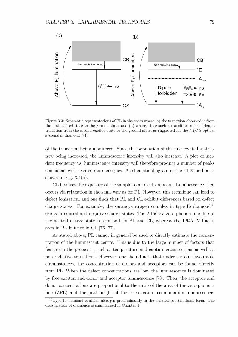
CHAPTER 3. EXPERIMENTAL TECHNIQUES 79
(a)
CBNon radiative decay
GS
Abo
ve E
illu
min
atio
n
νh
g
(b)
Dipoleforbidden
A 1/2
2
CBNon radiative decay
=2.985 eV
2
ν
gA
bove
E i
llum
inat
ion
E
h
1
2A
Figure 3.3: Schematic representations of PL in the cases where (a) the transition observed is fromthe first excited state to the ground state, and (b) where, since such a transition is forbidden, atransition from the second excited state to the ground state, as suggested for the N2/N3 opticalsystems in diamond [74].
of the transition being monitored. Since the population of the first excited state is
now being increased, the luminescence intensity will also increase. A plot of inci-
dent frequency vs. luminescence intensity will therefore produce a number of peaks
coincident with excited state energies. A schematic diagram of the PLE method is
shown in Fig. 3.4(b).
CL involves the exposure of the sample to an electron beam. Luminescence then
occurs via relaxation in the same way as for PL. However, this technique can lead to
defect ionisation, and one finds that PL and CL exhibit differences based on defect
charge states. For example, the vacancy-nitrogen complex in type Ib diamond10
exists in neutral and negative charge states. The 2.156 eV zero-phonon line due to
the neutral charge state is seen both in PL and CL, whereas the 1.945 eV line is
seen in PL but not in CL [76, 77].
As stated above, PL cannot in general be used to directly estimate the concen-
tration of the luminescent centre. This is due to the large number of factors that
feature in the processes, such as temperature and capture cross-sections as well as
non-radiative transitions. However, one should note that under certain, favourable
circumstances, the concentration of donors and acceptors can be found directly
from PL. When the defect concentrations are low, the luminescence is dominated
by free-exciton and donor and acceptor luminescence [78]. Then, the acceptor and
donor concentrations are proportional to the ratio of the area of the zero-phonon-
line (ZPL) and the peak-height of the free-exciton recombination luminescence.
10Type Ib diamond contains nitrogen predominantly in the isolated substitutional form. Theclassification of diamonds is summarised in Chapter 4

CHAPTER 3. EXPERIMENTAL TECHNIQUES 80
(a)
E
E
E
GS
E5
4
3
2
(b)
Tun
able
inci
dent
rad
iatio
n
E
E
E
E
GS
2
ν h
5
4
3
Figure 3.4: Schematic representations of (a) absorption and (b) PLE where transitions involvingall excited states are seen.
The calibration constant has been determined in a number of cases, and, in the
absence of any other major contaminants, this technique can be used to detect
concentrations of as low as 1010 cm−3 [79, 80].
Along with the ZPL, these optical techniques reveal transitions that are medi-
ated by one or more phonons, termed phonon side bands. The difference in energy
between the ZPL and a one-phonon side-band in equivalent to the phonon energy,
~ω. Hence, these methods can be employed to determine the local vibrational
modes of the defect responsible for the ZPL.
Now, as with the interpretation of IR-absorption, a key to assigning PL features
to atomic species are isotopic effects. The zero-point energy of an atom differs
for different isotopes and the optical transition energy therefore is also different.
However, care must be taken in interpreting results. The ZPL is related to difference
in the ground-state and excited-state total energies: 〈ΨGS|H|ΨGS〉 − 〈ΨEx|H|ΨEx〉.If these wavefunctions have no amplitude at one of the impurity atoms, then there
will be no isotopic shift due to that atom. This behaviour is exhibited in the T-line
in Si. Recent collaborative work between experiment and theory [12] has led to an
assignment of this optical centre to a complex containing two C atoms in a split
interstitial arrangement, with a H atom bound to one C. The ground and excited
wavefunctions of the electron states involved in the optical transition have a very
small amplitude on one of the C atoms. Consequentially the ZPL exhibits isotopic

CHAPTER 3. EXPERIMENTAL TECHNIQUES 81
fine structure consistent with the defect containing a single C atom. However, since
the C atoms are bonded to each other, phonon-assisted transitions exhibit isotopic
shifts consistent with a defect containing two C atoms.
As with other tools, uniaxial stress measurements can determine the symmetry
of the centre, as well as the symmetries of the electronic states involved in the
optical transition. This information is crucial to the establishment of a microscopic
structure, and can immediately eliminate possible charge states of a centre. For
example, as stated above, the trigonal vacancy-nitrogen centre in diamond occurs
in two charge states. The 2.156 eV ZPL system is known to possess a 2E ground
state. In the one-electron picture of the complex, the band-gap contains an a1- and
an e-level derived from the vacancy like t2-level. Thus, the e-level must contain
either one or three electrons to give the correct ground state symmetry, i.e. the
2.156 eV ZPL must arise from the neutral or the double negative charge state of
the N-V complex. This system is discussed in detail in Chapter 4. The manner
in which the peak positions change with stress can also give information about the
presence of other states in the gap, such as split off vibronic states due to Jahn-Teller
coupling [81].
Observing how ZPLs change with temperature can determine the energy split-
tings of nearby gap-states, such as in the 1.682 eV 12-line system in diamond. The
12 lines are believed to arise from three sets of four lines, one set for each isotope
of Si. Now, the four lines might arise from a transition from two types of systems.
1. A non-degenerate ground state to four nearby excited states.
2. Transitions between a double degenerate ground state to a doubly degenerate
excited state which have both been slightly split.
However, the change in relative intensities with temperature of the four lines would
be dramatically different for these two cases. Experiment shows that the ground
state is made up of two, slightly split levels, the separation being only 0.02 meV. In
Sec. 4.4 this centre is discussed in more detail. Time resolved optical measurements
give a measure of radiative lifetimes for individual ZPLs which can be modelled
theoretically (Sec. 2.17.2).
In summary, PL and related techniques can provide a wealth of information
about a defect, including symmetry, vibrational modes, and, in some cases, defect
concentrations. It can provide quantitative information on Jahn-Teller systems, and
a full picture of the electronic structure favourable situations. However, as with all
experimental techniques, the interpretation of the data requires care, and must
always be viewed in the context of other experimental and theoretical information.
CHAPTER 3. EXPERIMENTAL TECHNIQUES 82
3.5 Deep level transient spectroscopy
Deep level transient spectroscopy (DLTS) is a powerful method developed in the
1970s [82] to probe deep (>0.1 eV) electron and hole traps in the band gap. For a
review of the method, see Ref. [83].
In order to characterise a sample using DLTS, the sample must either be in the
form of a p-n junction or Schottky barrier. The characteristics of deep electron and
hole traps can then be determined by measuring changes in capacitance with time
and temperature. The method is powerful, and can determine values for the trap
energy11, the capture cross section, and the defect concentration. For the purposes
of this section I shall only examine the case of deep electron traps, but the principles
can easily be applied to hole traps.
Consider the system which is shown schematically in Fig. 3.5(a). The region to
the right of the junction is depleted of majority carriers due to the band bending,
with the depletion depth given as x1 in the reverse bias V1. This configuration thus
acts as a parallel plate capacitor with contact area A and has a capacitance
C1 =εrεoA
x1. (3.14)
When the bias is increased to V2, the capacitance decreases to a value C2, which
corresponds to the larger depletion region x2 (Fig. 3.5(b)).
To perform the DLTS measurement, the reverse bias V2 is applied, with a short
pulse of the reduced bias V1. When the bias returns to V2, the decrease in capaci-
tance is almost immediate, with the depletion region now being x3 > x2. However,
the filled traps in the region x2 < x < x3 are not in thermal equilibrium, and
over time lose their electrons to bring the depletion region, and hence the junction
capacitance back to C2. This decay process has an exponential form as shown in
Fig. 3.6.
The decay can be measured either as a transient current or a transient change in
capacitance. The latter is invariably adopted. The capacitance transient is written
as:
∆C(t) = C2 − C(t) (3.15)
= ∆C(0)et/τ (3.16)
where ∆C(0) is |C2 − C3| and τ is the lifetime of the electron in the trap, which
can be written as:
1
τ= σvNCe
−EC−ETkBT = en. (3.17)
11The trap energy is usually quoted with respect to a band edge: EC − ET for electron traps,and EV + ET for hole traps.

CHAPTER 3. EXPERIMENTAL TECHNIQUES 83
E
T
CE
FE
E
V
x
1Applied bias, V
E
λ x11
Ejunc
FE
E
E
x
2Applied bias, V
E
C
T
EV
λ 2
Ejunc
x2
Figure 3.5: Schematics of the conduction (EC) and valence (EV) bands bending at the p-n orSchottky junction. Plots are shown for two reverse biases, V1 and V2. The junction is located atx=0, and the distances xi and λi are described in the text.
σ is the capture cross-section of the electron trap, v is the average velocity of
electrons in the conduction band, and NC is the density of states in the conduction
band. en is simply the decay rate of electrons from the trap.
One possible measurable quantity using DLTS is an estimate of the trap concen-
tration. If the trap concentration, NT is much smaller than the donor concentration,
Nd, and if one assumes that NT is only weakly dependent on x, an approximate
value may be determined as follows. The capacitance of the junction for an applied
bias V1 is given as:
C1 = A
[εrεoe
2(V1 + Vjunc)
] 12 √
Nd,
where Vjunc is simply the potential difference across the junction for no applied
potential, and is indicated in Fig. 3.5. Hence,
dC1
C1
=1
2
dNd
Nd
.
One can then associate dC1 with ∆C(0) and dNd with NT to arrive at the expression
for the trap concentration:
NT =2∆C(0)Nd
C1. (3.18)
Eq. 3.17 shows that the decay rate is critically dependent on temperature, as
one might expect. This means that as the temperature is increased, the capacitance

CHAPTER 3. EXPERIMENTAL TECHNIQUES 84
2V
Vt
t
C
1
3C
2C
1
C
V
Figure 3.6: A plot of the reverse bias pulse and capacitance response.
returns to the equilibrium value more rapidly, as shown schematically in Fig. 3.7.
Also marked on this Figure is the ‘time window’, defined by the times t1 and t2.
An individual DLTS spectrum is obtained for a given time window by varying
temperature and plotting the change in capacitance (∆C) over the time window.
Such a plot shows the DLTS peaks characteristic of deep traps. A schematic DLTS
spectrum is shown in Fig. 3.8. Also indicated on Fig. 3.8 are the energies of the
traps, but in fact this picture is not strictly correct, since all terms in Eq. 3.17 are
dependent on temperature.
To determine an accurate value of ET , a series of measurements are performed
with different time windows. v and NC in Eq. 3.17 are proportional to T 1/2 and
T 3/2 respectively which means that Eq. 3.17 can be written
ln( en
T 2
)= χ−
(EC − ET
kB
)1
T,
where χ is a constant related to the natural logarithm of σ. Then, plotting ln(en/T2)
against T−1 gives a straight line with slope −(EC − ET )/kB. Trap energies can be
evaluated in this way to within a few %.
This plot can also be used to evaluate σ since the y-intercept is related to the
capture cross section. In practice, this method is not used since the resulting value
is not very accurate. An alternative method for estimating σ uses the fact that
for a sufficiently short applied bias pulse only a proportion of the traps will be
filled. As the pulse length is increased, the DLTS peak height increases due to more
traps being filled. Ultimately, the peak height will saturate as all the traps in the

CHAPTER 3. EXPERIMENTAL TECHNIQUES 85
T2
C∆
C t=0
<<<<
t
4
t 2
T3
T
1
C1
C3
t
4
0T
1T
3TT
T2
T1
T0
Figure 3.7: A graph showing how the capacitance transient changes with increasing temperature,T . T0 < T1 < T2 < T3 < T4. Also marked is the time-window for which the DLTS spectrum istaken. Note, for temperatures T0 and T4 there is no change in capacitance over the range of thetime-window.
depletion region are filled. The characteristic time for filling the traps, τ ′ is related
to the capture cross-section by the relation:
σ =1
τ ′vn,
where n = Nd −NT ≈ Nd is the effective doping concentration. Thus, an Arrhenius
plot of peak height against pulse length can be used to evaluate σ.
Finally, it should be noted that Eq. 3.18 is only an approximate expression for
the trap concentration. The derivation of this expression uses the depletion length
x1 as determined from Eq. 3.14. However, the correct distance is that from the
interface to where the trap energy crosses the Fermi-level. This is denoted by λ in
Fig. 3.5. This error can be accounted for by including a correction factor to the
right hand side of Eq. 3.18,x2
2
λ21 − λ2
2
.
λ can be determined from:
λ = x−(
2εrεo(EF − ET )
e2(Nd −NT )
) 12
,
which is itself dependent on the trap concentration, NT . Thus, NT must be evalu-
ated from the corrected version of Eq. 3.18 iteratively.
In summary, the use of DLTS to characterise deep traps can provide the theorist
with valuable information. The position of the trap level in the gap can be calculated

CHAPTER 3. EXPERIMENTAL TECHNIQUES 86
E
T
T2ET1E E
C∆
T3
Figure 3.8: A plot showing a typical DLTS spectrum. There are three peaks which correspondapproximately to the energies of three deep traps.
approximately using AIMPRO. DLTS has been used to investigate a large number
of centres, specifically the deep traps in GaAs produced by radiation damage, and
transition metals in Si.

Chapter 4
Vacancy-X complexes in diamond
‘... His party, cried “Advance and take thy prize
The diamond;”’ but he answer’d, “Diamond me
No diamonds! for God’s love, a little air!
Prize me no prizes, for my prize is death!
Hence will I, and I charge you, follow me not.”’
Alfred Tennyson from ‘Idylls of the King. Lancelot and Elaine.’
4.1 Introduction
Diamond has, for many centuries, fascinated mankind. The hardness, thermal
conductivity as well as the rarity and aesthetic appeal of diamond gem-stones has
led to scientific as well as commercial interest. Moreover, the availability of synthetic
diamond has led to the a desire to develop techniques for discriminating between
the more valuable gem stones and the man-made samples.
Diamonds can be grown using a number of techniques, the most important
of which are the high temperature, high pressure (HTHP), and chemical vapour
deposition (CVD) methods. During the development of diamond growth techniques
a number of materials with properties similar to diamond have been produced.
These include what is termed ‘diamond-like carbon’ and ‘tetrahedral amorphous
carbon’. Diamond-like carbon can be produced in large area films at relatively
modest expense, and diamond coating has made it into the realm of high-street
fashion: Rayban has recently put diamond coated sunglasses onto the market [84]
costing about £30 more than the untreated variety. They are reputed to have a
ten-fold increase in lifetime!
Viewed from an electronics point of view, these materials contain both sp2 and
sp3 bonded carbon. This leads to an effective lowering of the conduction band
bottom, and n-type semiconducting samples can be produced.
87

CHAPTER 4. VACANCY-X COMPLEXES IN DIAMOND 88
Ia Nitrogen is present in the form of aggregates of severaltypes.
IaA The N-aggregates are predominantly in the form of A-centres – substitutional N pairs.
IaB The N-aggregates are predominantly in the form of B-centres – a vacancy surrounded by four N atoms.
Ib Nitrogen is present in the form of isolated substitutional(deep) donors, Ns.
IIa Contains undetectable concentrations of N and B impuri-ties – these diamonds are rather rare.
IIb Contains no detectable nitrogen but has substitutionalboron giving a variety of shades of characteristic blue colourdepending on the concentration. Such diamonds are (p-type) semiconductors.
Table 4.1: A summary of the classification of diamonds.
Diamonds can be classified according to the content and form of nitrogen and/or
boron in the sample, and a summary is presented in Table 4.1. This system was
developed for natural diamond samples. Each form of nitrogen complex is char-
acterised by an absorption band from which the concentration of each defect type
can be estimated. Naturally, this categorisation is rather broad, and in practice
there are different forms of N-related defects in each sample – diamonds with A-
and B-centres are termed type IaA/B.
Besides the mechanical properties of diamond, technologically the most impor-
tant characteristic of diamond is its transparency to visible and infrared light. This
has led to the use of diamond for lenses in IR-detectors and in optical windows for
scientific equipment.
Optical properties are most often related to defects within diamond. The small
carbon mass generates substantial electron-phonon coupling, which together with
the high degeneracy associated with symmetric defects, often leads to important
and subtle Jahn-Teller (J-T) effects. A brief description of the J-T effect is given in
Appendix B. The high purity and large band gap of diamond facilitate experimental
studies of isolated centres in great detail. Positron annihilation studies [85] show
that vacancies are common defects in chemical vapour deposited (CVD) diamond.
They can occur in aggregates with concentrations up to 50 ppm which persist up
to 1100C. At a temperature around 600C neutral vacancies begin to migrate [86],
and readily complex with impurities creating further optically active defects.
In Sec. 4.2 a brief review of the single vacancy is presented, followed by vacancy-
nitrogen (Sec. 4.3) -silicon (Sec. 4.4) -phosphorus (Sec. 4.5) and -hydrogen com-
plexes (Sec. 4.6). The conclusions from all the V-X centres are summarised in the

CHAPTER 4. VACANCY-X COMPLEXES IN DIAMOND 89
final section.
4.2 The vacancy
As indicated in the introduction, the presence of vacancies and related centres leads
to absorption and emission in the diamond samples, and hence colour. Vast amounts
of experimental and theoretical work has been published on the matter, and it is
not practical to present a detailed review of the literature here. Instead, I present
a summary of the the current understanding of the optical and electronic structure
of the neutral and negatively charged vacancy.
The early theoretical work of Coulson and Kearsley [87] using a ‘modified linear
combination of atomic orbitals’ approach suggested that the unrelaxed vacancy
possesses a filled (orbitally non-degenerate) a1- and a partially filled (orbitally
triply-degenerate) t2-level in the band-gap made up from combinations of the four
‘dangling-bond’ orbitals.
In the negative charge state the vacancy has the electronic configuration a21t
32. It
is believed that this gives rise to the ND1 optical-band (3.149 eV), which has been
shown to be a transition between A and T electronic states [88]. EPR and ENDOR
studies [89] have determined that V− possesses a 4A2 ground state, consistent with
the optical data, and shows that Hund’s rule is obeyed (S=3/2). This result has
been reproduced theoretically many times [15, 90, 91, 92, 93].
The neutral charge state of the vacancy is somewhat more complicated due to
the t2 level containing only two electrons and hence giving rise to T2 ⊗ T2 mul-
tiplets: Coulson and Kearsley lists the possible symmetries of the a21t
22 electronic
configuration as (adopting their notation):
1A1 + 1E + 3T1 + 1T2.
Thus the one-electron configuration with two electrons in the t2 level gives rise
to these four many-body configurations. Similarly, the one-electron excited state
(a11t
32) gives rise to the eight many-body states
5A2 + 3A2 + 3E + 1E + 3T1 + 1T1 + 3T2 + 1T2.
Transitions can occur between multiplets with the same spin1, provided that the
transition is symmetry allowed. For example, only transitions from T1 and T2 states
are allowed to an E state. The neutral vacancy, V0, is believed to be responsible
for a number of optical features of which GR1 (1.673 eV) is most prominent. This
1Transitions involving a change in effective spin do exist, but are generally much weaker thanspin conserving transitions.
CHAPTER 4. VACANCY-X COMPLEXES IN DIAMOND 90
band arises from an electronic transition between a 1E ground state and a 1T2
excited state. Now, both the a21t
22 and a1
1t32 one-electron configurations possess
states with 1T2 symmetry. However, it is believed [87, 94] that the GR1 band does
not involve the transition of an electron between one electron states, but instead
from a transition between multiplets arising from the a21t
22 electron configuration.
This ‘internal transition’ is possible due to the high symmetry of the centre.
Provided Hund’s rule is obeyed, trigonal (e.g. vacancy-impurity) centre related op-
tical features necessarily involve the transition of an electron between one-electron
states. This follows since the only electron configuration that gives rise to multiplets
is e2: E ⊗ E gives rise to 3A2 + 1E + 1A1. Hund’s rule requires the ground state
to possess 3A2 symmetry (as in the case of the negatively charged vacancy-nitrogen
complex below), and transitions between this and the other two states does not
conserve spin.
Returning to V0, it is worth noting that the von Barth method (Sec. 2.16)
for estimating multiplet energies is not available due to an inadequate number of
independent Slater determinants. However, the calculated multiplet structure due
to Coulson and Kearsley is in agreement with the experimental observations of the
GR1 band, and has formed the basis of the interpretation of other vacancy related
centres.
4.3 Vacancy-nitrogen complexes
One of the most thoroughly studied vacancy-impurity complexes is the vacancy-
nitrogen, [V-N]−, complex (see for example Refs. [95, 96, 97, 98]) . This trigonal
centre gives an emission peak at 1.945 eV which has been correlated with an S=1
EPR centre [95]. In samples exposed to relatively high levels of neutron irradiation,
and hence where the Fermi-level is relatively low [99], the 1.945 eV line has a
decreased intensity whilst a new line at 2.156 eV grows. It is suggested that the
neutral [V-N] defect is responsible for the 2.156 eV optical transition. Recently [100],
an S = 12
EPR centre attributed to this centre was observed. Other [V-Nn] defects
also exist: the H3 centre for n=2; the N3 centre for n=3 and the B centre for n=4.
All but the B-centre2 are known to be optically active [101, 102].
The energy levels of the C3v [V-N] defect can be understood from those of a
perturbed vacancy [93, 104]. As discussed above, the vacancy introduces a filled
a1 and partially filled t2-level into the band gap. For neutral [V-N], where a N
atom replaces one of the neighbours of the vacancy, the t2-level is now occupied
by three electrons and lies above the occupied a1-level. In fact the results of these
2Absorption has been tentatively associated with the B-centre – see Ref. [102].

CHAPTER 4. VACANCY-X COMPLEXES IN DIAMOND 91
calculations show that the a1-level was pushed downwards towards the valence band
leaving a t2-level deep within the band gap. The trigonal symmetry of [V-N] splits
t2 into a filled a1 state lying below an e-level containing one electron. Thus it is
expected that [V-N] possesses an S=1/2 ground state.
In the negative charge state, the e-level contains two electrons and thus the
system can possess an effective spin of either S=1 or S=0 resulting in 3A2,1A1
and 1E states. If the orthonormal e-orbitals are denoted by x and y, then the
many-body states constructed from the pair of electrons occupying these orbitals
are:
Ψ(3A2) =1√2(x1y2 − x2y1)
α1α2
(α1β2 + α2β1)/√
2β1β2
Ψ(1A1) = (x1x2 + y2y1)(α1β2 − α2β1)/2
Ψ(1E) =(x1y2 + x2y1)(x1x2 − y1y2)
(α1β2 − α2β1)/2
The energies of these states can be evaluated using the method outlined in Sec. 2.16
where the determinental configuration wave-functions |x1 ↑ y2 ↑〉, |x1 ↑ x2 ↓〉, and
|x1 ↑ y2 ↓〉 give the energies of 3A2,12(1E + 1A1) and 1
2(1E + 3A2), and hence each
multiplet.
4.3.1 Cluster and basis.
The structure of the nitrogen-vacancy and tri-nitrogen-vacancy complexes are mod-
elled using 70 atom clusters centred on the vacant site: NC34H35 and N3C32H35. The
basis adopted for each of the atomic species are listed in Table 4.2. In each case,
the 16 atoms (two shells) in the centre of the cluster were in big basis, as defined
in Sec. 2.18.
Atom Wavefunction Charge densityN 4 × sp 5C 4 × sp 4H 2 × sp 3
Table 4.2: The atomic basis used for the calculations in Sec. 4.3.
In diamond, structures and energies are insensitive to the presence of bond-
centred Gaussians, and consequentially, the relaxation was performed without in-
cluding these. For calculations of transition energies, rates and the multiplet ener-
gies, the basis was increased so that all but the surface H atoms were in ‘big-basis’.

CHAPTER 4. VACANCY-X COMPLEXES IN DIAMOND 92
4.3.2 The vacancy bordered by a N atom
The relaxed [V-N]− (S=1) defect has trigonal symmetry with three N-C bond
lengths at 1.44 A. The bond lengths of the three C radicals are 1.45 A. The Kohn-
Sham energy levels revealed the t2-derived a↑1- and a↓1- levels (occupied) to lie 1.08
and 1.32 eV below the e↑- and e↓-levels. The Kohn-Sham levels in the region of
the band-gap are plotted in Fig. 4.1. The wavefunctions of the e-levels have little
amplitude on N in agreement with EPR studies [95] and are derived from the three
radicals of the vacancy, as indicated in Fig. 4.2. The total energies of the electronic
configurations gave the 3A2,1E, 1A1 ordering of the multiplets, with energies of
0.00, 0.44 and 1.67 eV respectively. Thus, in agreement with experiment, Hund’s
rule is satisfied.
−1.0
0.0
1.0
2.0
3.0
4.0
5.0
6.0
7.0
Ene
rgy
(eV
)
a1
a1
e
a1
a1
e
a1
a1
e
[V−N]1−
(S=1) [V−N]1−
(S=0) [V−N]0
Figure 4.1: The spin-polarised Kohn-Sham eigenvalues for the V-N complex in diamond. Only thestates in the region of the gap are plotted. Arrows indicate occupation and spin, and the emptyboxes show empty states. The ‘valence band tops’ have been aligned to facilitate comparison.
Now consider the optically excited state found by promoting an electron from
a↓1- to the e↓-level. This leaves a single hole in the e-level and corresponds to a 3E
term. The vertical excitation energy is the energy difference of these configurations
and differs from the ZPL by the relaxation energy of the excited state. A transi-
tion state calculation gave an optical energy of 1.77 eV in fair agreement with the
1.945 eV experimentally observed for 3A2 → 3E. The radiative lifetime of ∼20 ns,
compared to the experimental value of 13±0.5 ns [76] is found using the expression

CHAPTER 4. VACANCY-X COMPLEXES IN DIAMOND 93
0.00
0.03
0.05
0.08 0.13
-0.02
-0.0
2-0
.02
-0.05
0.00
0.00
0.00
-0.10-0.12
0.03
0.03
0.00
0.00
C N
V
Figure 4.2: A contour plot for one of the e-level wavefunctions (au) of [V-N]−. The plane passesthrough the vacancy site which is at the centre of the plot, and also through the N and one Catom. Note that the level is nodal at the N atom. The second e-level is qualitatively similar.
in Sec. 2.17.2. It is worth re-emphasising that estimates of the radiative lifetime
are sensitive to the transition energy and spatial extent of the wavefunction. If the
experimental transition energy is used in this expression, the estimated lifetime is
reduced to 15 ns.
For neutral [V-N], the e-level contains one electron and hence the ground state
has 2E symmetry. A transition from the a1-level to the e-level (Fig. 4.1) is allowed.
A transition state calculation estimates the energy to be 1.57 eV, and radiative
lifetime is estimated to be 20 ns, which is broadly in agreement with the 2.156 eV
observed 2E → 2A1 transition [81] which has a ∼ 29 ns lifetime [106]. This estimate
is reduced to ∼10 ns if the experimental transition energy is used. The ground state
permits a dynamic J-T effect and an A2-level is then expected to lie close to the 2E
ground-state [103]. The additional 2A2 → 2A1 optical transition3 has been detected
about 100 cm−1 below the 2.156 eV line.
In both charge states of [V-N], there is a filled a1-level just above the valence
band top, and a transition from this level to the e-level has an energy of 3-3.5 eV,
and a radiative lifetime of the order of 1 ns. This (extremely fast) transition has an
energy in the nitrogen absorption band, and as a consequence may not be observed.
In any case it is not likely to be responsible for either the 1.945 or 2.156 eV spectra.
It is worth noting that if the N atom is moved from a site neighbouring the
vacancy to one lattice site separation, the total energy of the cluster increases by
3This transition is forbidden in the C3v point group, but can be induced under stress.

CHAPTER 4. VACANCY-X COMPLEXES IN DIAMOND 94
∼3.3 eV in the neutral charge state. However, the dissociated system would act
more like isolated V− and N+s . This would give rise to an associated Coulomb
energy
−e2
εr,
which amounts to around 1 eV.
The large value of the stabilisation energy has important implications. One
would expect these centres to be stable to high temperatures. However, before they
dissociate, one might expect them to migrate. In fact, the idea of ‘vacancy-enhanced
aggregation of nitrogen’ [76] has long been mooted.
4.3.3 The vacancy bordered by three N atoms
For the [V-N3] defect, the ordering of levels in the band-gap is the reverse of the
[V-N] centre, with the a1-level derived from the vacancy t2-level now lying above the
e (Fig. 4.3). This a1-level contains just one electron in the neutral charge state, and
−10.0
−9.0
−8.0
−7.0
−6.0
−5.0
−4.0
−3.0
−2.0
−1.0
0.0
1.0
Ene
rgy
(eV
)
a1
e
a1
e
a1
a1
e
a1
a1
Ground Excited(N3) Excited(N2)
Figure 4.3: The spin-polarised Kohn-Sham eigenvalues for the [V-N3]0 complex in diamond. Shownare the 2A1 ground state, and the 2E excited state associated with the N3 optical transition. Alsoshown is an 2A1 excited state which is found to be the lowest in energy. This is associated withthe N2 vibronic centre. Only the states in the region of the gap are plotted. Arrows indicateoccupation and spin, and the empty boxes show empty states.
is largely localised on the C dangling bond. No J-T effects are then expected for the
ground state of this defect. The excited state generated by promoting an electron

CHAPTER 4. VACANCY-X COMPLEXES IN DIAMOND 95
from the e-level to fill the a1-level possesses 2E-symmetry, and might undergo a J-T
distortion, but this is not experimentally observed [105]. The S = 12
EPR centre
labelled P2 has been correlated with the N3 optical centre [107, 108].
The calculated N-C bond lengths are 1.43-1.44 A and the C-C bond lengths of
the unique C atom are 1.46 A. The e → a1 transition state energy at 2.8 eV is in
good agreement with the observed value of 2.985 eV for the 2A1 → 2E transition,
and the calculated radiative life-times are 10 and 8 ns using the calculated and
experimental transition energies respectively.
Now, the interpretation of the experimental data for the decay times of the
N3 centre is rather complex [74]: the lifetime not only varies with temperature,
but there is a strong sample dependence, which appears to be correlated with the
concentration of A-centres. At low temperature, the seven samples reported in
Ref. [74] have decay times ranging with increasing A-centre concentration from 18
to 41 ns. The temperature dependence for any particular sample assumes that there
is some thermal activation from the excited state of the N3 transition to a lower
excited state. The lower excited state is associated with the N2 vibronic system.
Then the experimentally observed decay time, τ , is given by the expression:
1
τ≈ 1
τrad+ νe−EA/kBT , (4.1)
where τrad is the true radiative lifetime of the N3 transition, ν is an attempt fre-
quency and EA is the activation energy. The temperature dependent term is a
phonon-assisted decay into the excited state of the N2 system which is directly
correlated with the N3 centre [74, 108]. The temperature effect is significant above
temperatures around 500 K. Using a least squares fit, the parameters in Eq. 4.1 are
found to be found to be τrad = 41 ns, ν = 590± 200 ns−1, and EA = 530± 20 meV
for the sample with lowest A-centre concentration. If a theory including tunnelling
effects is used, the fit to experiment is poor, and gives a value of τrad = 150 ns.
The fact that there is no ZPL associated with N2 suggests that this lower excited
state may have A2 symmetry, since transitions between A2 and A1 states are not al-
lowed in C3v. If this is the case, this presents a serious problem to the interpretation
of these ab initio results: the only way to construct a multiplet which transforms
as A2 is from an e2 electronic configuration. This can be done by exciting the two
electrons from the e↓-level in Fig. 4.3 to give a e2a21a
11. This would be higher in
energy than the 2E state.
In principle, the undetected state may be A1 symmetry, provided that the dipole
moment of the centre is aligned in such a way that 〈ΨA1|r.E|ΨA1〉 = 0. Thus, the
hidden state may arise from an a11e
4a21 electron configuration, i.e. the a1-level above
the valence band is depopulated. However, one would expect this to be a high energy
CHAPTER 4. VACANCY-X COMPLEXES IN DIAMOND 96
system (a transition state calculation would place such a transition at 4.7 eV), and
in these calculations the dipole matrix element shows that a transition would be
allowed, so a ZPL would be expected.
An alternative excited state is found by exciting the electron from the partially
filled a1-level to the a1-level above it. The resulting KS-levels are also plotted in
Fig. 4.3, and this is in fact a lower excited state (by around 0.5 eV) than that with2E symmetry. More significantly, the dipole matrix element 〈A1|r|A1〉 is orders of
magnitude smaller than 〈A1|r|E〉, consistent with the N2 centre. The much longer
lifetime of this transition is due mainly to the highly dispersed nature of this second
a1 KS-level.
Naturally, there are many further excited states that can be generated from
arrangements of occupancies of the e, and two a1-levels. The most likely of these is
the e3a11a
11 configuration which possesses an energy around 0.7 eV higher in energy
than the 2E excited state.
4.3.4 Conclusions
To conclude, in the case of the [V-N] complex, the theory is able to account for the
ground state electronic structure, the symmetries of the principal optical transitions
with semi-quantitative estimates of their energies and rates.
Furthermore, the multiplet structure assigned to [V-N3] has been reproduced
although the first excited state is found to be of A1 rather than A2 symmetry.
However, the calculated radiative lifetime of the 2A1 → 2E transition is too short
by at least a factor of four.
4.4 The vacancy-silicon complex
A number of experiments over the past ten years have added evidence to the idea
that Si can be present in the form of isolated impurities in diamond. Initial stud-
ies where natural diamonds were implanted with Si ions [109] revealed an optical
feature near 1.68 eV, which at the time was attributed to lattice damage due to
the proximity in energy to the GR1 band. However, the same signals were seen
in CVD diamond where the substrate was made of Si [110] or where the growth
chamber was made of fused silica [111], and the common Si-factor led to suggestions
that Si may be present in the form of an interstitial or Si-X complex. Combining
the requirement for Si with the fact that the 1.68 eV line is enhanced when the
vacancy becomes mobile [112], naturally leads to the assignment to some form of
vacancy-silicon complex.

CHAPTER 4. VACANCY-X COMPLEXES IN DIAMOND 97
In contrast to the single or double luminescence lines that arise from the [V-N]
centres, the 1.682 eV ZPL was resolved into complex set of twelve photo-luminescent
and absorption peaks [113]. Each of the three naturally occurring Si isotopes ac-
count for a set of four lines, representing a transition from an orbitally twofold
degenerate ground state, split by 0.20 meV, to a doublet excited state split by
1.07 meV. The results presented here show that the origin of these doublets lies in
the extraordinary structure of the [V-Si] defect.
4.4.1 Cluster and basis.
The silicon-vacancy complex is modelled using a 85 atom cluster centred on a bond:
SiC42H42. The basis adopted for each of the atomic species are listed in Table 4.3.
The central six C atoms and the Si atom were treated in ‘big basis’ as described
in Sec. 2.18. For the calculation of transition energies and rates, the bases was
augmented by including a single bond-centre in all but C-H bonds.
Atom Wavefunction Charge densitySi 4 × sp 5C 4 × sp 4H 2 × sp 3
Bond-centres 1 × sp 1
Table 4.3: The atomic basis used for the calculations in Sec. 4.4.
4.4.2 Results
In contrast to the [V-N] defects, the Si atom is unstable at the lattice site and
spontaneously moves to the split-vacancy site yielding a defect of D3d symmetry
as illustrated in Fig. 4.4. The separation between the Si atom and its six nearest
neighbours for the neutral cluster is 2.01 A, and is relatively insensitive to the
charge state, being 2.00 A in the negative charge state. The six dangling bonds
form two gap e-levels (Fig. 4.5) whose states are made up of bonding and anti-
bonding combinations. The lower level is filled and possesses odd parity (e′′), whilst
the upper is half-filled and has even parity (e′). These calculations show that the
S=1 spin configuration is around 0.25 eV more stable than S=0 thus agreeing with
Hund’s rule. The orbitally non-degenerate 3A′2 ground state rules out this charge
state as a candidate for the 1.682 eV band.
However, the position of the deep e-levels shown in Fig. 4.5, suggests that the
defect can readily act as an acceptor in synthetic or type Ib diamonds and in the
negative ionised case, the upper e′-level has a single hole leading to a 2E ′ ground

CHAPTER 4. VACANCY-X COMPLEXES IN DIAMOND 98
z
y
x
Figure 4.4: A schematic representation of the relaxed split-vacancy geometry of the V-Si complex.The solid circles represent C atoms, the empty circle the relaxed Si site, and the dashed circlesthe diamond lattice sites.
state. An internal optical transition can then occur between the e-levels leading
to a 2E ′ → 2E′′
optical line at 1.86 eV in good agreement with the observed line
at 1.682 eV. The doublets are likely to be split by spin-orbit or more likely a J-T
effect. The radiative lifetimes of the transition are estimated to be 3 ns using the
calculated transition energy, and 2 ns using the experimental value, which is in
excellent agreement with experimental value of 1-4 ns [114].
In a similar calculation to that performed for [V-N]0, the energy increase in
separating the vacancy and Si by a lattice site is found to be 0.32 eV. This is a
much smaller stabilisation energy due to (at least in part) the large strain around
a substitutional Si atom.
Preliminary calculations show that in [V-Ge], the impurity does not prefer this
site but remains at a C site pushing away its three C neighbours, although a
metastable configuration exists in the split-vacancy structure.

CHAPTER 4. VACANCY-X COMPLEXES IN DIAMOND 99
−3.0
−2.0
−1.0
0.0
1.0
2.0
3.0
4.0
5.0
6.0
7.0
8.0
Ene
rgy
(eV
)
e//
e/
e//
e/
e//
e/
[Si−V]1−
[Si−V]0(S=0) [Si−V]
0(S=1)
Figure 4.5: The spin-polarised Kohn-Sham eigenvalues for the V-Si complex in diamond in theregion of the band gap. The notation is as in Fig. 4.1, and the ‘valence band tops’ aligned.
4.5 The vacancy-phosphorus complex.
4.5.1 Introduction
There has been a considerable amount of work carried out on incorporating phos-
phorus in diamond with the aim of making a shallow donor defect. However, almost
all studies have succeeded in making highly resistive material despite substitutional
P (Ps) being expected to behave as a donor [115, 116, 117]. Electron paramagnetic
resonance (EPR) provides some evidence for Ps [118], and a second P defect is
found in P doped diamond grown by the high pressure method [119]. The latter
defect is trigonal with very little spin density at the P nucleus.
P has also been incorporated into chemical vapour deposition grown (CVD) dia-
mond by adding PH3 to the gas phase [120, 121]. Nitrogen apparently increases the
incorporation of P within the films yielding concentrations as high as 3×1019 cm−3
(as measured via SIMS). In spite of these large concentrations, the films were highly
resistive. PL experiments revealed broad intense bands around 1.7 eV which in-
creased with [P]. These were assigned to donor-acceptor pair recombination al-
though the identities of the defects are not known. Significantly, no sharp optical
lines due to P or the vacancy were detected.
Success at making conducting, n-type diamond has been achieved through a

CHAPTER 4. VACANCY-X COMPLEXES IN DIAMOND 100
cold implantation of P ions followed by rapid thermal annealing [122]. It may be
that this process rapidly removed vacancies resulting from the implantation.
CVD diamond usually contains a high concentration, up to ≈ 5 × 1018 cm−3 of
vacancies [85]. The lack of an optical signal due to vacancies in the P rich material
suggests that they are bound up with P in some form. As with the N-V and Si-V
centres, a P-V complex may be understood in terms of the vacancy.
It might be thought that the P-V defect would be similar to N-V. In that case
we would expect it to act as an acceptor, with spin 1 in the ionised state, and
to possess a sharp luminescence line arising from the a1 → e internal transition.
However, it shall be shown below that this is not the case and [P-V]− has spin S=0
and no internal optical transitions are possible.
P-V acts as a deep acceptor and would compensate substitutional P and N. This
would explain the insulating properties of P-rich diamond, the lack of P-related
sharp luminescent bands, as well as the presence of broad donor-acceptor optical
bands.
4.5.2 Cluster and basis.
The calculations for the P-V complex have been performed on a 85 atom cluster in
the same way as the Si-V complex. The basis used is given in Table 4.4. The initial
runs had the central (P+6C) atoms in ‘big basis’ (Sec. 2.18).
Atom Wavefunction Charge densityP 4 × sp 5C 4 × sp 4H 2 × sp 3
Table 4.4: The atomic basis used for the calculations in Sec. 4.5.
4.5.3 Results
Previously [117], substitutional phosphorus has been examined using AIMPRO: it
is found to be an on-site defect with a (resonant) LVM around 380 cm−1.
In the first case the P atom was placed as far away from the vacancy and the
surface as possible. The structure was relaxed in the neutral charge state. Then the
P atom was moved to border the vacancy and the cluster re-relaxed. The energy
in this case was lower by 1.5 eV than the case where P was separated from the
vacancy. This shows that substitutional P is unstable in the presence of vacancies
and readily forms the P-V complex.

CHAPTER 4. VACANCY-X COMPLEXES IN DIAMOND 101
In the P-V complex, the P atom did not remain at its lattice site but drifted
away until it lay mid-way between two lattice sites as with the split-vacancy Si-V
complex. Fig. 4.4 can also be used to understand the inner core of the relaxed
86 atom (D3d) cluster. The six P-C separations are 2.00 A, the same as the Si-
C distances in the negative Si-V complex. In fact the only difference in the two
systems is the species of the impurity at the centre. The reason for the stability of
the split-vacancy is partially connected with the large atomic size of P although Ge-
V does not appear to assume the same structure. Fig. 4.6 shows the spin-polarised
Kohn-Sham energy levels of the P-V defect in the vicinity of the band gap, together
with those of a similar sized cluster without any defects. These reveal a mid-gap
e′-level (even) containing three electrons and an e′′-level just above the valence band
top, resulting in an effective spin of S=1/2. The position of this mid-gap level is
qualitatively similar to that found in the Si-V defect and thus the defect would be
expected to trap electrons arising from say substitutional N or indeed P. Thus the
P-V defect acts as a deep acceptor. However, the e′ levels are then filled and the
defect must be diamagnetic and no internal optical transitions are possible.
−2.0
−1.0
0.0
1.0
2.0
3.0
4.0
5.0
6.0
7.0
Ene
rgy
(eV
)
e//
e/
e//
e/
(a) (b) (c) (d)
Figure 4.6: Kohn-Sham eigenvalues of the [P-V] complex in diamond in vicinity of the band gap.The arrows and filled boxes denote spin polarised and non-polarised occupied levels respectivelyand the empty boxes empty levels. (a) An 86 atom cluster representing pure diamond. (b,c) Spin-polarised levels for the neutral P-V defect. Note the e′′↑-level is full and the e′↓ level is half-filledgiving a 2E′ ground state. (d) shows the levels of [P-V]− where all gap levels are filled.
When the Fermi-level is low, such as for example when the material is irradiated

CHAPTER 4. VACANCY-X COMPLEXES IN DIAMOND 102
or the absence of substitutional N, then a neutral P-V defect would be formed having
S=1/2. The wave-functions of the e′ gap levels are combinations of sp3 orbitals on
the six C atoms surrounding P and possess very little amplitude on P itself as shown
in Fig. 4.7. The trigonal symmetry of the defect and the fact that the spin density
-0.15-0.00
-0.0
0-0
.45
0.15
-0.00
-0.00
0.30
0.45
0.60
0.75
1.20-0
.15
-0.1
5
-0.00 0.15
-0.1
50.
30
0.30
0.45
0.45
0.60
1.05
-0.00-0.45-0
.60
-0.0
0
[11-2]
[111
]
Figure 4.7: The pseudo-wavefunction for an e′′↑ state (au×10). Note that the amplitude near Pis negligible.
is very low on P suggests that this defect might be the EPR centre investigated in
Ref. [119].
Although no internal optical transitions are possible for the ionised defect, neu-
tral pairs of N+ and (P-V)− defects could luminesce and be the source of the broad
band donor-acceptor recombination band observed in Ref. [121]. The luminescence
energy would then be given by the difference in energies of the (excited) system
containing the neutral N and P-V centres:
E(N0) + E([P − V ]),and the (ground state) system containing the ionised centres:
(E(N+) + E([P − V ]−)) − e2
εr
.
Note, the energy of the ionised system includes the Coulomb interaction energy4.
With the N donor level and the P-V acceptor level (Fig. 4.6) at Ec − 1.7 eV and
approximately Ec − 2.7 eV respectively (where Ec is the conduction band edge),
then for r about 5 A, this transition would be around 1.5 eV, close to the observed
value.4The Coulomb energy, e2/εr = 13.606× 2/5.5r which = 0.26 eV for r=10A.

CHAPTER 4. VACANCY-X COMPLEXES IN DIAMOND 103
4.5.4 Summary
In conclusion, the calculations suggest a strong binding energy of P with vacancies.
In the P-V centre, the P atom lies mid-way between two vacancies. The centre
has D3d symmetry with spin S=1/2 in the neutral charge state, and there is little
spin-density on the P atom consistent with EPR experiments. The defect acts
as a deep acceptor and together with N would explain the pronounced broad PL
bands seen around 1.7 eV in P-doped diamond. The defect could also compensate
remaining substitutional P atoms, provided that there are vacancies present in the
sample5. This would explain the difficulties in making phosphorus electrically active
in diamond.
4.6 Vacancy-hydrogen complexes
4.6.1 Introduction
It is well known that hydrogen readily complexes with vacancies in silicon; infrared-
absorption experiments [13] have shown that VHn, n = 1, 2, 3, 4, defects are present
in ion-implanted samples. Furthermore, it is well established that impurities trap
hydrogen, such as SiGa in GaAs [123], P in Si [124], B in Si [125], and it has been
suggested that similar effects may be seen in diamond [126].
However, the location of H in diamond is not universally agreed upon, despite
numerous studies. It is well known that CVD grown samples can contain as much
as 1 at.% of H [127], but it is believed that most of this lies at grain boundaries
and surfaces.
Calculations have provided evidence that if H exists in an isolated form in bulk
diamond, it would preferably occupy a bond centre [128, 129, 130], with the tetra-
hedral interstitial site being variously reported to be between 1.7 and 2.7 eV higher
in energy.
It has been suggest [131, 132, 133] that hydrogen may also be being trapped at A-
centres (neighbouring substitutional N atoms). Recent calculations [134] suggested
that the saving in energy by moving a single H atom from the bond-centred site to
that in between the two N atoms is around 4 eV. The intermediate stage where the
H atom is adjacent to only one of the N atoms is 3 eV higher in energy than the
N-H-N system. So it seems clear that if isolated H atoms exist in bulk diamond,
they would prefer to occupy sites in the lattice close to other defect sites.
H2 might be present in molecular form, and calculations predicted that a centre
with a H2 molecule in an interstitial space would be stable [135]. However, later it
5This is highly likely in the P-implanted samples.

CHAPTER 4. VACANCY-X COMPLEXES IN DIAMOND 104
was shown that a system made up of one bond-centred H and one anti-bonded was
much lower in energy (by 3.3 eV). This structure has since been termed H∗2, and is
seen in Si [136] and Ge [137]. A similar centre is believed to exist in GaAs [138].
Experiment has provided a number of clues as to the presence of H in diamond.
IR-absorption studies [139] have reported C-H related stretch and wag LVMs at 3107
and 1405 cm−1 respectively. H on the 〈111〉 surface of diamond has a fundamental
stretch mode somewhat lower [140] at 2829 cm−1. This suggests that the C-H bond
giving rise to the 3107 cm−1 band is somewhat shorter, perhaps reflecting a more
confined local environment.
Cathodoluminescence (CL) has revealed the presence of optically active H-
related centres [141], with a ZPL at 540 nm (2.30 eV), close to the feature seen
in H-implanted natural diamond [142] which persists up to 1000C and exhibits iso-
topic shifts with deuterium. The 540 nm line appears to arise from centres located
at grain boundaries.
A number of EPR studies have reported signals that might be related to H-
dangling-bond centres [73, 143, 144, 145]. In Refs. [73, 145] two signals are reported
labelled H1 and H2, with estimated separations between the unpaired electron spin
and nuclear spin of 1.9 and 2.3 A respectively. It has been suggested that these
centres are highly distorted hydrogenated vacancies, where two of the dangling
bonds reconstruct to leave a unique radical. Ref. [143] suggests that the defects are
dispersed throughout the sample, and thus the centre is simply V-H, whereas the
later studies suggest that the experimental evidence is more consistent with centres
close to grain boundaries where local distortions are rather strong. In Ref. [73], a
number of cluster-calculations where reported, which supported the assignment of
the H1 signal to a single H at a perturbed V site.
4.6.2 Cluster and basis
Reported here are the atomic and electronic structure of VHn, n = 1 − 4, with
their LVMs. The calculations were performed on (70+n)-atom clusters (HnC35H35)
centred at the vacant lattice site. The basis used is summarised in Table 4.5, with
the central 4C+nH defect atoms in ‘big-basis’ as described in Sec. 2.18. Further
relaxation calculations were performed on the larger 130+n-atom cluster HnC70H60.
For electronic structure calculations, the relaxed structures were embedded in a
186+n-atom cluster HnC104H82. In the case of the divacancy, a bond-centred, 85-
atom cluster was used(HC42H42).

CHAPTER 4. VACANCY-X COMPLEXES IN DIAMOND 105
Atom Wavefunction Charge densityC 4 × sp 4H 2 × sp 3
Bond-centres 1 × sp 1
Table 4.5: The atomic basis used for the calculations in Sec. 4.3.
4.6.3 VH
VH was relaxed with a single hydrogen placed ∼ 1.1 A along the 〈111〉 direction
from one of the C atoms neighbouring the vacancy. All but the surface H atoms
were allowed to relax. The final H-C bond was 1.053 A, and the distance between
the H and the three unsaturated C atoms at 2.028 A, where these atoms have
relaxed away from the vacancy site by around 12%. The C bonded to the hydrogen
relaxed by around 10%.
Now, Zhou et al. suggest that the S = 12
EPR centre arises from unpaired spin
centred at one of the unsaturated C atoms, and analysis of the hyperfine anisotropy
provides an estimate of a ∼ 1.9 A separation between the electronic and nuclear
(hydrogen) spin. This is in good agreement with the VH geometry as calculated
here. Note, the experimental estimate of the separation is not the H-C separation,
but the H-C-dangling-bond distance. This is less than the inter-atomic distance.
In order to model the electronic structure of the VH complex, the relaxed geom-
etry taken from the 70-atom cluster was embedded in a larger (187-atom) cluster,
and the self-consistent KS-levels calculated. The KS-eigenvalues for the neutral
VH complex are plotted in Fig. 4.8. The defect gives rise to filled singlet below a
doublet containing only a single electron, where both levels are deep in the gap,
and could give rise to 2E → 2E ⊗ 2E internal optical transitions. If it is assumed
that the system is analogous to the [V-N]0 centre, the lowest excited state is 2A1,
although the calculations have not been performed to confirm this. A transition
state calculation predicts the transition energy to be about 1.1 eV (1127 nm). The2E ground state is a candidate for a Jahn-Teller distortion. The electronic structure
indicates that the defect could act both as a donor, or more likely, as an acceptor.
In the positive charge state, the re-relaxed geometry puts the H 1.046 A from
the C to which it is bonded, and 2.072 A from the remaining unsaturated atoms.
The KS-levels are also plotted in Fig. 4.8. The doublet is now completely empty,
and the singlet level lies around 2 eV below. This defect would be EPR inactive,
but could give luminescence: a transition state calculation predicts a transition at
around 1.2 eV.
In the negative charge state, the defect can adopt either a S = 1 or an S = 0
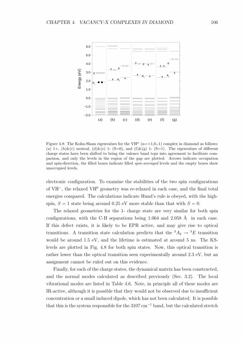
CHAPTER 4. VACANCY-X COMPLEXES IN DIAMOND 106
−2.0
−1.0
0.0
1.0
2.0
3.0
4.0
5.0
6.0
Ene
rgy
(eV
)a1
e
a1
e
a1
e
a1
e
(a) (b) (c) (d) (e) (f) (g)
Figure 4.8: The Kohn-Sham eigenvalues for the VHn (n=+1,0,-1) complex in diamond as follows:(a) 1+, (b)&(c) neutral, (d)&(e) 1- (S=0), and (f)&(g) 1- (S=1). The eigenvalues of differentcharge states have been shifted to bring the valence band tops into agreement to facilitate com-parison, and only the levels in the region of the gap are plotted. Arrows indicate occupationand spin-direction, the filled boxes indicate filled spin-averaged levels and the empty boxes showunoccupied levels.
electronic configuration. To examine the stabilities of the two spin configurations
of VH−, the relaxed VH0 geometry was re-relaxed in each case, and the final total
energies compared. The calculations indicate Hund’s rule is obeyed, with the high-
spin, S = 1 state being around 0.25 eV more stable than that with S = 0.
The relaxed geometries for the 1- charge state are very similar for both spin
configurations, with the C-H separations being 1.064 and 2.058 A in each case.
If this defect exists, it is likely to be EPR active, and may give rise to optical
transitions. A transition state calculation predicts that the 3A2 → 3E transition
would be around 1.5 eV, and the lifetime is estimated at around 5 ns. The KS-
levels are plotted in Fig. 4.8 for both spin states. Now, this optical transition is
rather lower than the optical transition seen experimentally around 2.3 eV, but an
assignment cannot be ruled out on this evidence.
Finally, for each of the charge states, the dynamical matrix has been constructed,
and the normal modes calculated as described previously (Sec. 3.2). The local
vibrational modes are listed in Table 4.6. Note, in principle all of these modes are
IR-active, although it is possible that they would not be observed due to insufficient
concentration or a small induced dipole, which has not been calculated. It is possible
that this is the system responsible for the 3107 cm−1 band, but the calculated stretch

CHAPTER 4. VACANCY-X COMPLEXES IN DIAMOND 107
mode is (for the neutral charge state) some 10% higher. Now, as is discussed in more
detail in Chapter 6, a 10% change in LVM can be obtained from around a 3% change
in bond length, which is around the tolerance of AIMPRO. In the VH complex in Si
which has been identified experimentally [13], the stretch mode was overestimated
by 9%6. In fact, increasing the C-H bond length in the VH complex by around 3%
increases the total energy by only around 30 meV but decreases the stretch mode
to 3114 cm−1, which is in much better agreement with the experimental mode.
However, due to a lack of experimental data, no firm assignment can be made.
1+ Neutral 1-(S=1) 1-(S=0)H D H D H D H D
3563 2607 3411 2501 3214 2350 3240 2372
Table 4.6: The H/D stretch modes (cm−1) associated with four charge/spin states of VH.
4.6.4 VH2
If the assignment of the H1 centre to VH is incorrect, and in fact H2 arises from this
centre, it is possible that H1 arises from a vacancy where more than one dangling-
bond is saturated by H. This suggestion was originally made in Ref. [145].
The calculations performed in a similar way to those for VH but where either
two or three of the vacancy’s dangling-bonds are decorated with H indicate that the
more H present, the shorter the unsaturated C to H distance, in broad agreement
with this alternative model.
VH2 is C2v with the two equivalent H atoms lying 1.049 A from their C neigh-
bours. The unsaturated C atoms lie 2.008 A from the closest hydrogens. The
relaxation of the C atoms away from the vacancy site is slightly less pronounced
in this case with the two unsaturated C atoms moving around 12% further from
the vacancy centre and those bonded to H relax by around 11%. The electronic
structure, as plotted in Fig. 4.9, indicate that there is a filled a1-level around 1 eV
below an empty b2-level, both of which lie mid-gap. A transition state calculation
on a1 → b2 predicts an energy of around 0.9 eV. Around 0.5 eV above the valence
band maximum is a filled b1-level, and there could possibly be a transition from
this level at around 3 eV. A transition between levels with b1 and b2 symmetry is
not allowed.
For VH2 to be responsible for the reported S = 1/2 g = 2.0028 EPR-signal,
it would have to adopt either a positive or negative charge state. In the positive
6The observed mode assigned to VH is at 2068 cm−1 whereas the calculations find the VHstretch mode to be 2248 cm−1.
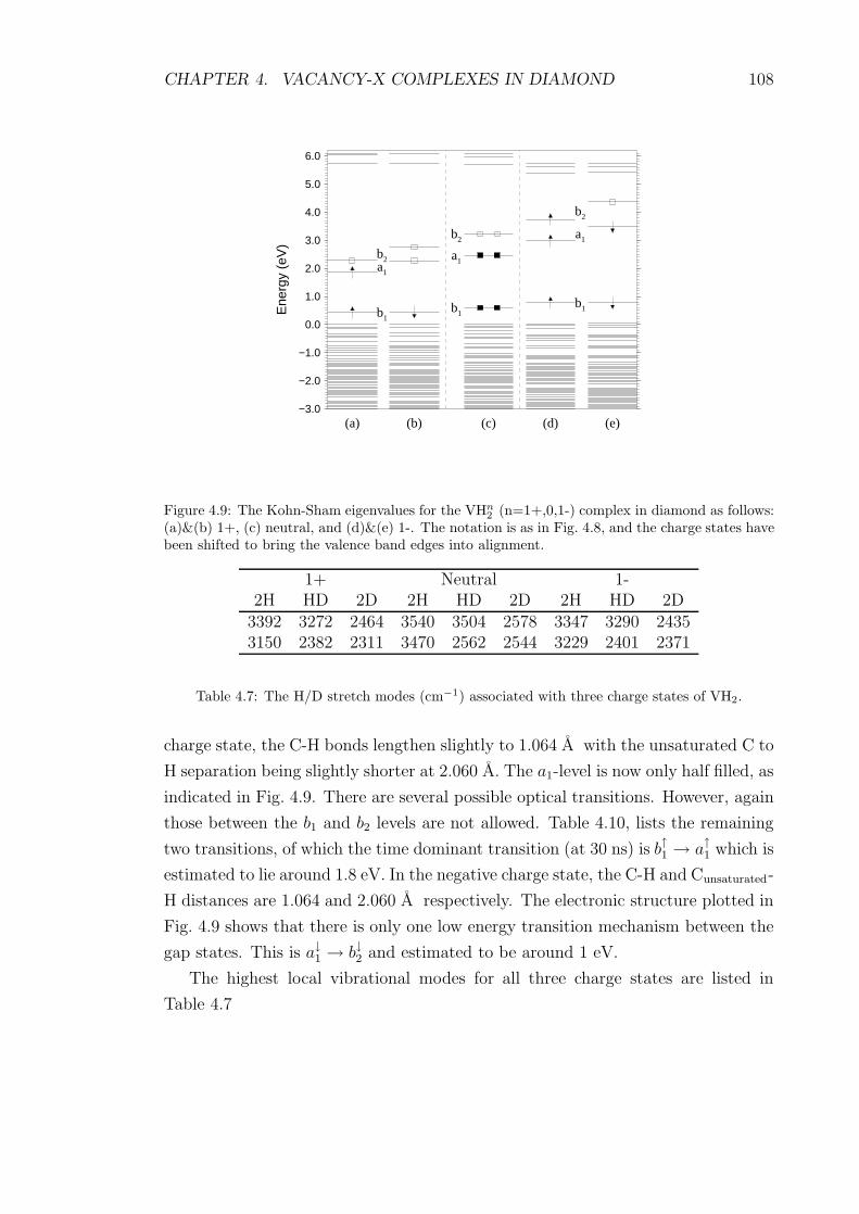
CHAPTER 4. VACANCY-X COMPLEXES IN DIAMOND 108
−3.0
−2.0
−1.0
0.0
1.0
2.0
3.0
4.0
5.0
6.0
Ene
rgy
(eV
)
b1
a1
b2
b1
a1
b2
b1
a1
b2
(a) (b) (c) (d) (e)
Figure 4.9: The Kohn-Sham eigenvalues for the VHn2 (n=1+,0,1-) complex in diamond as follows:
(a)&(b) 1+, (c) neutral, and (d)&(e) 1-. The notation is as in Fig. 4.8, and the charge states havebeen shifted to bring the valence band edges into alignment.
1+ Neutral 1-2H HD 2D 2H HD 2D 2H HD 2D
3392 3272 2464 3540 3504 2578 3347 3290 24353150 2382 2311 3470 2562 2544 3229 2401 2371
Table 4.7: The H/D stretch modes (cm−1) associated with three charge states of VH2.
charge state, the C-H bonds lengthen slightly to 1.064 A with the unsaturated C to
H separation being slightly shorter at 2.060 A. The a1-level is now only half filled, as
indicated in Fig. 4.9. There are several possible optical transitions. However, again
those between the b1 and b2 levels are not allowed. Table 4.10, lists the remaining
two transitions, of which the time dominant transition (at 30 ns) is b↑1 → a↑1 which is
estimated to lie around 1.8 eV. In the negative charge state, the C-H and Cunsaturated-
H distances are 1.064 and 2.060 A respectively. The electronic structure plotted in
Fig. 4.9 shows that there is only one low energy transition mechanism between the
gap states. This is a↓1 → b↓2 and estimated to be around 1 eV.
The highest local vibrational modes for all three charge states are listed in
Table 4.7

CHAPTER 4. VACANCY-X COMPLEXES IN DIAMOND 109
4.6.5 VH3 and VH4
VH3 is trigonal and has an effective spin S = 1/2 in the neutral charge state.
The electronic structure of the triply hydrogenated vacancy is the reverse of that
calculated for VH, i.e. the doublet lies below the singlet, and the singlet is partially
filled, as can be seen in Fig. 4.10. The singlet lies mid-gap, with the doublet around
0.6 eV above the valence band top. In analogy to [V-N3], this defect may give rise to
an 2A1 → 2E internal optical transition. Again, a transition state calculation was
performed, and the estimated energy is some 3.2 eV, and is likely to be obscured
by nitrogen related optical activity.
−8.0
−7.0
−6.0
−5.0
−4.0
−3.0
−2.0
−1.0
0.0
1.0
Ene
rgy
(eV
)
e
a1
VH3 VH4
Figure 4.10: The Kohn-Sham eigenvalues for the neutral VH3 and VH4 complexes in diamond.The notation is as in Fig. 4.8.
Although the fully hydrogenated vacancy is patently diamagnetic, and thus
cannot possibly be responsible for optical or EPR activity, for the sake of com-
pleteness, the structure of VH4 has also been calculated. The C-H bond-length is
only 1.023 A. The KS-levels indicate that there are two levels that may be in the
gap. However, since they are shallow and filled, the vacancy has been effectively
passivated (Fig. 4.10), and would not give rise to any optical activity.
The LVMs of the VHn (n=3,4) defects have also been calculated, and are listed
in Table 4.8. It is interesting to note that as the number of H atoms in the vacancy
increases, so does the frequency of the highest stretch mode. This follows from
the fact that as H is added to the vacancy, the Coulombic repulsion from the
neighbouring H atoms increases and the attraction from the remaining dangling

CHAPTER 4. VACANCY-X COMPLEXES IN DIAMOND 110
VH3 VH4 V2H3H 2HD H2D 3D 4H 3HD 2H2D H3D 4D H D
3571 3531 3489 2584 4039 3994 3946 3895 2907 3123 22933442 3441 2559 2522 3842 3842 3842 2877 28053440 2539 2522 2521 3842 3842 2851 2805 2805
3842 2827 2805 2805 2805
Table 4.8: The H/D stretch modes (cm−1) associated with the neutral VH3, VH4, and V2Hcomplexes.
bonds decreases. This leads to shortened C-H bond lengths and the LVMS are
pushed up in frequency. This is seen in the observations of analogous defects in
Si [13]. Note, in the case of VH4, the highest mode is rather high, but if a 10%
overestimation is present, this might be reduced to around 3600 cm−1. Furthermore,
this breathing mode would be infra-red inactive, and the second, degenerate mode is
the one that would be experimentally observed (including a 10% error gives around
3460 cm−1).
4.6.6 Stabilities of VHn
E(VHn) E(VHn−1-Hb−c) Stabilisation energyn (au) (au) (eV) [27.212 eV=1 au]1 -432.873 -432.757 3.162 -435.998 -435.883 3.143 -434.014 -433.919 2.604 -437.124 -437.045 2.15
Table 4.9: The total energies of the clusters containing VHn and VHn−1-Hb−c systems forn=1,2,3,4. Note that in all cases, H prefers to be located within the vacancy.
In order to estimate the stability of each of the VHn, n=1,2,3,4 centres, the
following calculations were performed. VHn and VHn−1+Hbond−centred were relaxed
in the larger (130+n-atom) cluster. Then, the difference in energy is an upper
bound on the stabilisation energy of each centre. The results are summarised in
Table 4.9.
These results show that vacancies, as one might expect, are deep hydrogen-traps,
but it should be noted that these energies are with reference to bond-centred H. As
discussed above, previous calculations have suggested that there are even deeper
traps in competition with these.

CHAPTER 4. VACANCY-X COMPLEXES IN DIAMOND 111
4.6.7 V2H
H1 possesses a H–dangling-bond distance of ∼ 1.9 A, but when the H concentra-
tions are much lower, this signal disappears to be replaced by the weaker H2 signal
with a separation around 2.3 A. The H–dangling-bond distance of 2.3 A is some-
what more than one would expect in a single vacancy, as confirmed by these and
other [73] calculations. Therefore, we suggest that this weaker defect may be a
divacancy containing hydrogen. We have relaxed an 85-atom cluster centred on a
bond between the two atoms that are removed to produce the divacancy, where a
single H is placed close to one of the C atoms neighbouring a vacancy. The C-H
bond length is found to be 1.078 A. Then the distances between the H and the
5 remaining dangling-bonds are 2.004, 2.005, 2.595, 2.596, and 3.060 A. The H/D
LVMs are listed in Table 4.8. The H and the unpaired electron spins are in different
halves of the divacancy, and therefore the measured interaction would be related to
the 2.6 A separation. This is in reasonable agreement with the experimental value
2.3 A.
4.6.8 Conclusion
In conclusion, we find that all four VHn, n = 1, 2, 3, 4 defects are stable and that
VH, VH±2 and VH3 are all consistent with the H1-EPR spectrum in terms of the
separation of the electronic and nuclear spins. However, the fact that experimental
evidence [73] points toward a single radical and a single H in the centre means
that the true origin of the EPR signal cannot be any of these. The modelling
outlined in Ref. [73] finds that the relaxed structure exhibits a weakly reconstructed
bond between two of the unsaturated C atoms neighbouring the vacancy. No such
reconstruction is seen in the calculations performed for this study.
All VHn complexes are optically active, and the various transitions are listed in
Table 4.10. It is possible that any one of these centres may give rise to the 540 nm
hydrogen-related CL peak reported in Ref. [141]. However, there is insufficient
experimental data to make any firm assignment. Furthermore, one would expect
these centres to possess characteristic LVMs, and an experiment correlating LVM-
absorption to the H1- and H2-EPR centres could provide valuable insight into their
atomic structure. However, EPR can detect much lower concentrations of defects,
and it is possible that IR-absorption experiments would not be able to resolve VH-
related modes.
Now, H in a vacancy is strongly bonded to C, but the remaining dangling-bonds
exert a Coulomb attraction on the proton. This tends to lengthen the C-H bond.
Thus, one might expect that as more H is added, the C-H bonds would shorten,

CHAPTER 4. VACANCY-X COMPLEXES IN DIAMOND 112
Defect Transition Energy (eV)
VH+ a↑1 → e↑ 1.2
VH0 a↑1 → e↑ 1.1
a↓1 → e↓ 1.4
VH−(S = 1) a↓1 → e↓ 1.5
VH+2 a↑1 → b↑2 0.8
b↓1 → a↓1 2.1
VH02 a1 → b2 0.9
VH−2 a↓1 → b↓2 0.9
VH03 e↓ → a↓1 3.2
Table 4.10: A table of the main optical transitions expected for VHn, n = 1, 2, 3 in diamond.
and consequently, the H-dangling-bond separation increases. Then if H1 is VH, H2
might be VHn, n > 1. However, this is inconsistent with the fact that H2 is only
seen in samples with a low [H].
More likely, as suggested in Ref. [73] H1 is the VH centre (either in the bulk or
close a grain boundary), and H2 is a related centre, also with a single H atom. This
is consistent with the model of the divacancy-hydrogen complex which possesses
a structure that is consistent with the 2.3 A separation. Furthermore, one might
expect that when there is more H around, the divacancy would trap one H atom
in each of the vacancies, and become diamagnetic. If the divacancy was a deeper
trap to the H than the single vacancy, then this would also lend weight to this
assignment.
Note, the calculations can not predict where in the sample VH centres would
lie, and it is quite possible that they would all be present in a region close to the
surface and grain boundaries.
4.7 Summary
In conclusion,
• The calculations give a good account of the optical properties of the [V-N] and
[V-N]− defects; the transition state calculations are in reasonable agreement,
as are the radiative lifetimes.
• Using the von Barth approach for calculating multiplet structure has proved
successful for [V-N]−.
• Although the calculated transition energy of the neutral [V-N3] centre is in

CHAPTER 4. VACANCY-X COMPLEXES IN DIAMOND 113
good agreement with experiment, the radiative lifetime is up to an order of
magnitude too short.
• Including the shallow KS-level in the electronic structure of this defect pro-
vides an explanation of the N2 vibronic centre which has been correlated with
N3. Further excited states are available, one of which is likely to give rise to
the N4 signal.
• The calculations show that the [V-Si]− defect possesses an unusual, D3d struc-
ture where Si occupies a split-vacancy site.
• These results point to [V-Si]− being responsible for the twelve optical lines seen
around 1.682 eV. This spectrum results from an internal transition between
two doubly-degenerate e-levels.
• The centre is paramagnetic but there is little wave-function amplitude at the
Si nucleus.
• A phosphorus-vacancy complex also adopts the D3d split-vacancy structure,
and would act as an acceptor. It is likely that P forming this centre is a reason
for the difficulty in producing n-type semiconducting samples.
• [P-V]− would not give rise to any sharp, internal optical transitions.
• An optical transition between [P-V] and the nitrogen donor may be responsible
for the broad 1.7 eV band seen in P-doped diamond samples.
• A complex of hydrogen with a vacancy produces an EPR (S=1/2) centre.
The deep vacancy t2-state is split into an e-level lying above an a1 and is
expected to give rise to an optical transition around 1.1 eV. It is possible that
a complex similar to this is responsible for the H1-EPR system.
• VHn, n=2,3,4 are also stable, and for n=2,3 the centre is expected to possess
deep gap states which would give rise to optical transitions. VH4 is completely
passivated.
• In all cases, there are large binding energies between impurities and vacancies.

Chapter 5
Nickel and Ni-X centres indiamond and Si
‘The best preparation for good work tomorrow is to do good work today.’
Elbert Hubbard.
5.1 Nickel in diamond
5.1.1 Introduction
Synthetic diamonds grown using high-pressures and high-temperatures (HPHT) are
produced by heating together a carbon source1 typically with a diamond seed crys-
tal2. The presence of a transition metal (TM) catalyst is not strictly necessary,
but the ‘direct conversion’ methods yield only small crystals (typically < 100 nm
grains [146]). The catalyst can take several forms [146], including water, phos-
phorus, and transition metals (e.g. Cr, Mn, Fe, Co, Ni). With a transition metal
catalyst typical temperatures3 and pressures for synthesis are 1400C and 5 GPa
respectively [146]. Growth rates vary between companies, but Ref. [146] lists typical
values of 2-15 mg/h. The largest example is that grown by De Beers at 2840 mg
(6 mg/h) which implies a growth time of nearly twenty days!
Despite the wide variety of transition metals used, until recently, the only one
found to contaminate the diamonds in the form of dispersed impurities was Ni, the
reason for which is not clear. Recently, however, photoluminescence and absorption
experiments have identified cobalt-nitrogen complexes [147].
1The C source is usually graphite, although other sources including SiC are used.2If a seed crystal is not used, spontaneous nucleation takes place at higher temperatures and
pressures.3For other catalysts, higher temperatures are required - for oxyacid salts the synthesis temper-
ature is above 1600C, and for H2O T∼2000C.
114

CHAPTER 5. NICKEL AND NI-X CENTRES IN DIAMOND AND SI 115
As the synthesis of diamonds using the HPHT has become more technologically
and commercially important, the need for characterisation of the diamonds pro-
duced using this method has prompted a great deal of experimental and theoretical
work.
In this Chapter, a number of Ni-related centres are examined, and comparisons
made to experiment and previous theory. The layout of the Section is as follows:
first the experimental results are described, then the theory of transition metal
impurities in diamond is outlined (Sec. 5.1.3). In Sec. 5.1.4 previous theoretical
studies of Ni+i and Ni−s are discussed, in Sec. 5.1.5.1 the approach used for this study
is described and the results are given in Sec. 5.1.5. Conclusions are in Sec. 5.1.6.
5.1.2 Experimental background
Ni impurities are known to occur in synthetic diamonds grown using the HPHT
method with solvent catalysts containing Ni. Since prominent optical features are
associated with these impurities, there have been great interest in these centres and
a wide range of experimental techniques have been used to characterise the defects.
5.1.2.1 Magnetic centres
EPR studies have unambiguously shown that substitutional nickel (hereafter re-
ferred to as Nis) exists in isolated form: the signal is isotropic even at 4 K, consistent
with an on-site defect and the ‘super-hyperfine’ interactions (from 13C) indicates
twelve next-nearest neighbours. A tetrahedral interstitial Ni impurity (hereafter
referred to as Nii) would possess only six such neighbours. This defect has been
associated with an optical transition at 2.51 eV [148, 149]. Various theoretical stud-
ies [150, 151, 152] have shown that TMs to the right of the periodic table possess a
partially filled t2-level in the band-gap, and in the case of Ni, the effective spin of
S = 32
suggests the negative charge state [25]. This is consistent with the relatively
high concentration of N-donors in samples exhibiting this EPR signal.
Two other EPR centres labelled NIRIM-1 and NIRIM-2 are associated with
nickel [153], tentatively in the interstitial site. They are observed in Ni-containing
synthetic diamond when the concentration of N is lowered by the addition of tita-
nium and/or zirconium getters to the melt. The NIRIM-1 signal (g = 2.0112, S =12) is isotropic at 25 K (implying Td symmetry) but anisotropic at 4 K where it
exhibits C3v symmetry. The signal is not observed in samples where Ni is not
present in the melt and is enhanced by the addition of boron dopants, suggesting
a positively charged defect, although the effect apparently disappears for high con-
centrations of B. This has led to speculation that Ni forms complexes with B [153],
but might just as well arise due to a change in charge state.
CHAPTER 5. NICKEL AND NI-X CENTRES IN DIAMOND AND SI 116
It has been suggested that this signal originates from isolated Ni+i slightly dis-
torted away from an interstitial Td site [153]. However, there are no super-hyperfine
measurements which would exclude an assignment to Ni+s . The latter model was
rejected due to the observation of the NIRIM-1 and Ni−s EPR signals in measure-
ments on the same sample. This argument is not conclusive: since if the material is
inhomogeneous, Nis could certainly exist in more than one charge state. Such inho-
mogeneity is illustrated by the fact that both the neutral (2.156 eV) and negative
(1.945 eV) charge states of the [V-N] complex coexist (Chapter 4).
NIRIM-2 (g = 2.3285, S = 12) exhibits trigonal symmetry at all temperatures.
It seems likely that NIRIM-1 is either Ni+i or Ni+s and NIRIM-2 is then a complex of
NIRIM-1 with an unknown acceptor X−. It was suggested that X is a vacancy [153],
but this seems unlikely if interstitial Ni is involved, as then Ni+i should easily mi-
grate to the vacancy forming Ni+s . On the other hand, if the Ni atom is in the
substitutional site, then one can imagine a vacancy at a neighbouring site being
energetically favourable, such as in the case of [P-V], [N-V] and [Si-V] complexes.
Other possibilities for an acceptor are boron or aluminium. The NIRIM-2 signal is
also enhanced by the addition of B although no hyperfine interactions with ‘X’ are
observed requiring the spin-density at ‘X’ to be small.
Finally, a class of EPR-defects labelled NE1-7 have been reported by Nadolinny
and Yelisseyev [154, 155]. They all involve Ni, and possibly a number of combina-
tions of vacancies and nitrogen, although the actual structures are speculative. One
interesting hypothesis in Refs. [154] and [155] is the formation of a split-vacancy
structure as seen in Si-V and P-V when Ni and a vacancy are combined. This then
forms the basis of aggregation of N atoms to form the more elaborate structures.
5.1.2.2 Optical centres
In samples where the concentration of N-donors is low (typically [Ns]<10 ppm), the
dominant optical feature is a pronounced optical band with a zero-phonon transition
at 1.40 eV superimposed on a broad band centre around 1.4 eV. The ZPL is made up
from two peaks separated by 2.7 meV [156], upon which is resolved fine structure
correlating with the natural abundances of the five Ni isotopes [157]. Uniaxial
stress [149] reveals that the 1.40 eV ZPL arises from a C3v centre. Nazare et al. [149]
then suggest that the NIRIM-2 EPR defect is responsible for this ZPL, although
this seems to be based largely on the fact that the centres are both trigonal and
exist in samples with low donor concentrations. The transition occurs between a2E ground state and an 2A excited state.
Other optical features seen in samples where [Ns] is low are peaks at 1.22 [158],
2.56 and 3.1 eV [159]. The lowest energy peak is believed to arise from a more

CHAPTER 5. NICKEL AND NI-X CENTRES IN DIAMOND AND SI 117
positive4 charge state of the 1.40 eV doublet. The 2.56 eV band is only seen in
luminescence and exhibits a complicated structure which has proved difficult to
interpret [160]: it is thought that Nis acts as an acceptor to another impurity
centre which is responsible for the ZPL. The peak at 3.1 eV also appears to exhibit
structure [159]. Both the 1.22 and 3.1 eV lines are only detected in absorption.
In samples containing concentrations of N exceeding ∼50 ppm, bands at 1.883
and 2.51 eV become dominant. Using uniaxial stress, Nazare et al. [161] found that
the 1.883 eV structure arises from a system with C2v symmetry. The 2.51 eV band
has only been reported in absorption.
An emission peak at 2.968 eV correlated with Ni has been observed in optical
detection of magnetic resonance experiments (ODMR) [162]. The ZPL associated
with the centre is very weak. The radiative lifetime of the transition is very long
(40 µs at low temperature).
Recently [163], samples containing Ni−s defects and high concentrations of Ns
impurities were annealed at 1900C. A complex set of ZPLs around 1.693 eV appear
at the temperature when Ns becomes mobile. These lines were not seen in samples
where Ni is absent and it is suggested that they are due to a complex containing
a single N close to a Ni impurity. The possibility that this complex is of the form
Ni−s -N+s is examined in this Chapter.
5.1.3 Electronic structure of Ni in group IV semiconductors
The electronic structure of TM impurities in group-IV semiconductors is often
discussed in terms of the Ludwig-Woodbury model (LW) [150] and the vacancy
model [151]. The 3dn4s2 atomic configuration of a first row transition metal atom5
is expected to be changed by the environment of the lattice: first, the crystal field
causes the 3d-levels to drop below the 4s-level, and secondly, the crystal field splits
the d-levels into e- and t2-levels.
First, according to the LW-model neutral interstitial impurities possess a t2-level
lying below the e and the 3dn+2 configuration becomes t62en−4. For Ni+i , the highest
state is then e3 which gives an S = 12
defect. This would thus be a candidate for
a Jahn-Teller distortion, but a distortion along 〈111〉 would not split the e-level.
Such a distortion might then cost energy. However, the spin-orbit coupling would
split the degenerate e-state when Ni+i is displaced along 〈111〉, and the consequent
lowering of energy might exceed the energy required to move Ni off-site. Since these
energy changes oppose each other, one would expect that the net lowering of energy,
4It is only observed in samples where [Ns] is very low (<5 ppm), resulting in a lower Fermienergy.
5For Ni, n = 8.

CHAPTER 5. NICKEL AND NI-X CENTRES IN DIAMOND AND SI 118
as well as the splitting of the e-level, to be very small and the effect would disappear
at temperatures when the upper level becomes occupied, or when kBT exceeds the
reorientation energy barrier.
This would explain why the anisotropic signal of NIRIM-1 at 4 K, attributed to
Ni+i , becomes isotropic at 25 K [153]. Indeed, the spin-orbit interaction splits the
e-level in the trigonal 1.4 eV optical defect by 2.7 meV [164] which corresponds to
34 K. Thus spin-orbit interactions have the correct order of magnitude.
However, an alternative viewpoint is prevalent [165, 166]: a chemical re-bonding
force drives Ni+i off-site. According to this model, Ni+i spontaneously distorts along
〈111〉. Now, chemical re-bonding forces are usually rather strong and this makes the
disappearance of the trigonal symmetry at temperatures as low as 25 K unlikely.
Substitutional N in diamond moves off-site by this mechanism and the reorientation
barrier between the equivalent minima is observed [167], and calculated [168], to be
0.7 eV. In the chemical re-bonding model, Ni+i should be identified with NIRIM-2
which is known to be a trigonal defect rather than NIRIM-1 and this leaves unre-
solved the assignment of NIRIM-1. The almost Td symmetry of NIRIM-1 suggests
a simple defect, such as Ni+i or Ni+s whereas there there many possibilities for the
trigonal NIRIM-2 centre involving pairs.
The LW-model for substitutional TM impurities places the e-level below the
t2-level. Now, the four sp3 bonds of the C atoms surrounding Ni form a1 and t2
states. The Ludwig-Woodbury model asserts that these t2-levels lie below those of
the TM and consequently are filled leaving n−6 electrons in the t2-levels of the TM
impurity. For Ni−s , the t2-level has three electrons which, if Hund’s rule operates,
yields an S = 32
state. This model implies that the highest occupied gap-levels are
localised on Ni.
On the other hand, the ‘vacancy’ model of substitutional TM impurities on the
far-right of the periodic table considers that the associated d−levels lie deep in the
valence band and couple weakly with the t2-levels arising from the Td symmetry of
the ideal vacancy, V [151, 152, 169, 170, 171]. Now V− has an electronic configura-
tion a21t
32 and if Hund’s rule is not obeyed, a Jahn-Teller distortion occurs leading
to a structure with C2v symmetry. This distortion splits the t2 level into an a1
lying below b1 and b2 [172]. In Si, Ni−s , Pd−s and Pt−s possess this C2v symmetry
although the level ordering is inverted from V−, i.e. b1, b2 and a1 [173, 174]. How-
ever, in diamond Hund’s rule is obeyed for V− and calculations similar to those
described here [93] show that the a21t
32, S = 3
2configuration has a lower energy than
a Jahn-Teller distorted S = 12
state.
Thus applying the LW-model or the vacancy model leads to the prediction that
Ni−s should exist in an S = 32
state. Notably they differ on the question of whether

CHAPTER 5. NICKEL AND NI-X CENTRES IN DIAMOND AND SI 119
the gap wavefunctions are mainly localised on Ni or on the C atoms surrounding it.
This is discussed below.
It is expected then that Nii can act as a donor whereas Nis acts as an acceptor.
The types of diamond in which these centres are founds suggests that these acceptor
and donor levels lie above the acceptor level due to B−s level at Ev+0.37 eV [175]
and below the donor level of N+s level at Ec-1.7 eV [176]. In fact, photo-EPR
experiments [177] show that Ni−s possesses an acceptor level at Ev+3.03 eV. These
experiments also support the correlation of the 1.883 and 2.51 eV ZPLs to Ni−s .
There is a possibility that Nis can act as a donor. This would require the t2 level
to lie in the upper part of the gap with an extended wavefunction so that correlation
effects are small. The levels of Ni+s would then be close to those of Ni−s . In Ni+s ,
the t2 level contains one electron and this would provoke a Jahn-Teller distortion.
If the distortion led to a trigonal defect, the t2 level splits into e and a1. It is not
yet clear whether the e-level would lie above or below the a1-state, but the splitting
is likely to be very small, and if the e-level is lower, a further spin-orbit splitting
is expected – just as in the Ni+i case. For such a distortion to disappear at 25 K,
as with NIRIM-1, either the interval between the split levels, or alternatively the
barrier to reorientation, must be less than around 2 meV.
5.1.4 Previous calculations
CNDO calculations (see Sec. 2.5.1) have been carried out [24, 165] on Nii and Nis.
Ni−s possesses Td symmetry in agreement with experiment. However, the ordering
of electronic gap levels appears to be at variance with experiment. Ni0s was found
to possess a filled mid-gap a1-level lying below the empty t2-level [165]. Tetrahedral
Ni−s must then have a t2-level containing one electron, which is plainly inconsistent
with the assignment of an effective spin S = 32.
This result may be affected by the positions of the nearest neighbours. If the
surrounding shell of C neighbours is allowed to relax outwards, the splitting between
the a21 and t12 states was reported to decrease, and it was suggested that eventually
they would cross giving a configuration t32a01 which is consistent with experiment.
Similar CNDO calculations were then carried out on Ni0i . In agreement with
the discussion above, a filled e-level was found to lie just above the valence-band
top. On removal of one electron this level moves to mid-gap. The tetrahedral
site was found, however, to be unstable and a structure with 1.5 eV lower energy
arises when Ni+i is moved 0.1 A along the [111] direction6, with the four nearest
neighbours allowed to relax. However, if the neighbours were held fixed, the nickel
6Here the convention that one neighbour is along [111] is adopted, and the distortion in the[111] direction is therefore towards three nearest C-neighbours.
CHAPTER 5. NICKEL AND NI-X CENTRES IN DIAMOND AND SI 120
atom moved 0.042 A along [111] towards a C neighbour. This C3v distortion does
not alter the degeneracy of the level, and cannot be attributed to a Jahn-Teller
effect since it does not raise the degeneracy of the e-level. It must therefore be
a chemical re-bonding effect. Subsequent to the observation of the 1.22 eV band,
the structure and transition energy of a Ni++i system was reported [178]. Here the
1.22 eV ZPL was assigned to a 3E →3 T1 transition at this centre. This would
suggest that a further EPR-active centre should be observed in low N samples.
Recently, Ni+i has been investigated using a discrete variational local density
functional method [166]. The calculations were based on clusters of 30 carbon atoms
around the central tetrahedral interstitial Ni atom with two types of boundary
conditions were applied: the first is a free boundary condition, in which the surface
dangling bonds are left unsaturated for calculation of the geometry of the defect,
and the second is a Watson sphere approach which enabled the electronic structure
to be found. Only the central five atoms were allowed to relax and the symmetry
constrained to be trigonal.
Again the on-site defect was found to be unstable. The Ni atom moved 0.2 A
from the Td site along [111], away from one C neighbour. When relaxed, this C
neighbour also moved along [111]. The total nearest neighbour relaxation lowers
the binding energy by around 8 eV. Such a distortion energy is far too big to
explain the properties of the NIRIM-1 signal. The ordering of gap levels leads to
the electronic configuration e4a21e
3. The shortest resulting Ni-C bond-length (which
lies along [111]) is just 1.52 A, with the other three Ni-C bonds being 1.58 A. These
are surprising short bond lengths. The Ni-C bond-length observed in the Ni(CO)4
molecule is 1.84 A [179], and one would have expected the large Ni atom to have
repelled the surrounding carbon atoms. These calculations also led to assignments
to this defect for the experimentally observed optical transitions at 1.40 and 3.1 eV.
It appears then that previous calculations identify Ni+i with the NIRIM-2 defect.
5.1.5 AIMPRO calculations
5.1.5.1 Cluster and basis
The atomic basis used in the calculations for this chapter are listed in Table 5.1.
In each case, the central defect atoms and their neighbours were treated using a
‘big-basis’ as defined in Sec. 2.18, with the remaining atoms in ‘minimal-basis’. In
the case of Ni+i B−s , additional orbitals were placed on bond-centred sites around
the central 6 atoms. The clusters used consisted of 71 atoms centred on the Ni
impurity atom with the surface dangling bonds saturated with hydrogen atoms.
Substitutional defects are modelled using the tetrahedral cluster NiC34H36, whereas

CHAPTER 5. NICKEL AND NI-X CENTRES IN DIAMOND AND SI 121
Atom Wavefunction Charge densityNi 7 × spd 14B 4 × sp 5N 4 × sp 5C 4 × sp 4H 2 × sp 3
Bond-centres 1 × sp 1
Table 5.1: The atomic basis used for the calculations in Sec. 5.1.
interstitial Ni was modelled using the cluster, NiC30H40, centred on a Td interstitial
site. In the case of the Ni-vacancy complex, a bond-centred cluster was adopted:
NiC42H42.
It should be noted that since the charge density is fitted using s-Gaussians, a
large number of functions are required to adequately fit the highly peaked charge
density of d-orbital elements. This can lead to near singularities in the inversion of
the density matrix. Consequently the results presented here should be regarded as
near to or at the limit of stability of the current incarnation of AIMRPO.
5.1.5.2 Nickel carbonyl
The Ni-basis7 has been tested on the relatively simple Ni(CO)4 molecule, which
is ideally suited due to the tetrahedral structure and Ni-C bonds. The Ni-C and
C-O bond lengths have been determined experimentally to be 1.837 and 1.141 A
respectively [179]. AIMPRO produced optimised bond lengths of 1.819 and 1.150 A,
errors of just 1.0 and 0.8%. These results provide confidence that the basis used
well describes the structural behaviour of Ni-C bonds.
5.1.5.3 Interstitial Ni+
This defect was found to remain on-site retaining Td symmetry in contrast to the
previous calculations described above. In order to confirm the stability of the defect,
the nickel atom was displaced along [111], towards one of the C neighbours, by
0.4 A. Then it, and its four nearest C neighbours were allowed to relax. The Ni
atom returned to the tetrahedral site with the four nearest carbon neighbours at
a distance of 1.72 A. The six next-nearest neighbours were at 1.78 A. This cluster
was then relaxed further with all the atoms allowed to move. This resulted in an
expansion and the final structure has Ni-C nearest neighbour lengths of 1.84 A
and next nearest neighbour lengths of 2.00 A. This shows that there is extensive
7For this calculation all atoms were in ‘big-basis’, and additional bond-centred functions wereplaced between C and O atoms.
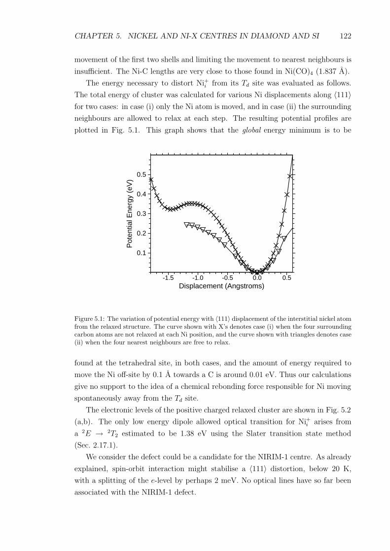
CHAPTER 5. NICKEL AND NI-X CENTRES IN DIAMOND AND SI 122
movement of the first two shells and limiting the movement to nearest neighbours is
insufficient. The Ni-C lengths are very close to those found in Ni(CO)4 (1.837 A).
The energy necessary to distort Ni+i from its Td site was evaluated as follows.
The total energy of cluster was calculated for various Ni displacements along 〈111〉for two cases: in case (i) only the Ni atom is moved, and in case (ii) the surrounding
neighbours are allowed to relax at each step. The resulting potential profiles are
plotted in Fig. 5.1. This graph shows that the global energy minimum is to be
-1.5 -1.0 -0.5 0.0 0.5Displacement (Angstroms)
0.1
0.2
0.3
0.4
0.5
Pot
entia
l Ene
rgy
(eV
)
Figure 5.1: The variation of potential energy with 〈111〉 displacement of the interstitial nickel atomfrom the relaxed structure. The curve shown with X’s denotes case (i) when the four surroundingcarbon atoms are not relaxed at each Ni position, and the curve shown with triangles denotes case(ii) when the four nearest neighbours are free to relax.
found at the tetrahedral site, in both cases, and the amount of energy required to
move the Ni off-site by 0.1 A towards a C is around 0.01 eV. Thus our calculations
give no support to the idea of a chemical rebonding force responsible for Ni moving
spontaneously away from the Td site.
The electronic levels of the positive charged relaxed cluster are shown in Fig. 5.2
(a,b). The only low energy dipole allowed optical transition for Ni+i arises from
a 2E → 2T2 estimated to be 1.38 eV using the Slater transition state method
(Sec. 2.17.1).
We consider the defect could be a candidate for the NIRIM-1 centre. As already
explained, spin-orbit interaction might stabilise a 〈111〉 distortion, below 20 K,
with a splitting of the e-level by perhaps 2 meV. No optical lines have so far been
associated with the NIRIM-1 defect.

CHAPTER 5. NICKEL AND NI-X CENTRES IN DIAMOND AND SI 123
−3.0
−2.0
−1.0
0.0
1.0
2.0
3.0
4.0
5.0
6.0
7.0
8.0
Ene
rgy
(eV
)
t2
e
e
e
e
a1
e
e
(a) (b) (c) (d)
Figure 5.2: A schematic representation of the electronic structure (Kohn-Sham eigenvalues) ofthe two interstitial Ni defects examined in this work. (a) and (b) correspond to the Ni+i spin upand spin down electronic levels respectively, with the arrows signifying filled states and the boxesempty states. Similarly, (c) and (d) corresponds to the up and down KS-levels of the Ni+i -B−
s
complex. The levels have been shifted linearly to facilitate comparison.
5.1.5.4 The Ni+i -B−s complex
Ni+i might be expected to complex with negatively charged acceptors and hence
the Ni+i -B−s defect has been investigated. Here B is substituted for one of the four
nearest C neighbours and the cluster then allowed to relax. Ni moves slightly away
from the Td site along 〈111〉, by 0.16 A. The boron atom relaxes radially outwards
(along [111]), with a relaxed Ni-B bond-length of 1.98 A. The three C neighbours
also relaxed outwards with final Ni-C bond-lengths of 1.87 A.
The electronic structure (Fig. 5.2(c,d)) can be understood as arising from that
of Ni+i where the t2-levels are split into an e- and a1-level by the trigonal symmetry.
It is assumed that the a↑1-level drops into the valence band. The highest occupied
e↓-level contains a single hole 2.4 eV below the lowest empty, (anti-bonding) a↓1state, giving the system a 2E ground state. The corresponding e↑-level is filled, and
lies 3.7 eV below the unoccupied a1-level which is believed to represent the conduc-
tion band edge. The least energetic optical transition would be between the e↓- and
an e↓-level 1.2 eV below. Such a transition is not consistent with the experimen-
tally observed symmetries of Ni-related optical reanstitions. A second low-energy
transition between the e↓- and a↓1-levels (∼1.8 eV). As discussed in Sec. 5.1.5.9, the
CHAPTER 5. NICKEL AND NI-X CENTRES IN DIAMOND AND SI 124
estimated transition rate via these route are rather low compared to the 2.4 eV
e↓ → a↓1 transition corresponding to 2E → 2A1.
The C3v symmetry of the final structure, the 2E and 2A1 ground and excited
states and the effective spin of S = 12
are all consistent with an assignment to the
1.4 eV and NIRIM-2 centres. No strong hyperfine interaction with B would be
expected, or is observed, because the hole occupies an e state which has a node at
the B site. Hence Nii-B or possibly Nii-Al complex are candidates for these defects.
Transition state calculations have been performed on the two optical transitions
highlighted above. a↓1 → e↓ gives 1.61 eV, and the e↓ → a↓1 is 2.78 eV. Although the
higher energy transition is calculated to be the more rapid, there may be several
reasons for discounting it. First, and most important, identifying a1-level with the
bottom of the conduction band would suggest a broad optical feature, contrary
to experiment. Secondly, a conduction state is rather diffuse, and the artificial
confinement of the cluster would therefore exaggerate the dipole matrix element for
this transition.
If B rather than Al is involved, and since B possesses two naturally occurring
isotopes, one might expect that the optical line would be split by zero-point motion
effects of the two isotopes. This follows as the frequencies of the defective lattice are
different in the ground and excited states. However, the effect would not occur if the
ground and excited state wavefunctions had nodes at the B site. This splitting would
be in addition to the 2.7 meV splitting due to spin-orbit coupling. No additional
splitting is observed in the 1.4 eV centre. Now, although the e wavefunction is
nodal at the B site, the a1 wavefunction is not. Hence, the model implies a splitting
for B although it might not be resolvable as for example the absence of isotopic fine
structure in the 856 meV ZPL in Si [12].
The conclusions are that this defect remains a possible candidate for the 1.4 eV
ZPL and the NIRIM-2 EPR centres.
5.1.5.5 Substitutional Ni−
The cluster containing the substitutional defect, Ni−s , was relaxed with an effective
spin of S = 32. The inner 17 atoms (three shells of C atoms) were allowed to move.
Ni remained on the Td site with four nearest-neighbours at 1.89 A and the twelve
next-nearest neighbours at 2.58 A. The pseudo-wavefunction associated with one
of the filled t↑2 states possesses a nodal surface between the Ni and neighbouring C
atoms (Fig. 5.3) but it is difficult to draw definite conclusions as to the localisation
of the pseudo-wavefunctions: there is always a near nodal surface through C as a
consequence of using pseudo-potentials.
The spin-polarised energy levels are shown in Fig. 5.4(a,b). The highest occupied

CHAPTER 5. NICKEL AND NI-X CENTRES IN DIAMOND AND SI 125
0.0
0.0
0.0
0.0
0.0
0.0
0.0
0.00.0
0.0
-0.4
-0.4
0.4
0.4
-0.8
0.8
0.0
0.0
0.4
0.8
0.8
-0.81.2
0.4
-0.4
-0.80.8
0.0
0.0
Figure 5.3: A contour plot of the pseudo-wavefunction associated with one of the three Ni−s t↑2states taken through the 110 plane; the x-axis is along 〈001〉, and the y-axis along 〈110〉. Thewavefunction amplitude is in au×10. The Ni atom is at the centre of the plot and marked with thewhite square. The two C atoms are marked with black circles. The plot shows the anti-bondingcharacter of the wavefunction, i.e. there is a node in the wavefunction between the Ni atom andits four C neighbours.
spin-up energy level has t2 symmetry and lies 3.0 eV above another occupied t2 spin-
up level and 3.1 eV below an unoccupied spin-up singlet which is believed to be
the bottom of the conduction band. The corresponding empty spin-down t2-levels
are 1.7 eV above an occupied doublet. These results suggest dipole allowed optical
transitions around 1.7 and 3.1 eV whereas an observed transition occurs around
2.51 eV [148].
If a transition state calculation is performed, then the average energy of the
transition between the e- and t2-levels is 2.33 eV.
Note, a transition to the conduction band is likely to be rather broad, and it
is therefore not likely that this transition is responsible for any of the sharp ZPLs
correlated with Ni. The experimentally observed transition at 1.883 eV found in
N-rich material [159] is also thought to be related to the substitutional defect.
The same cluster was then relaxed with effective spin of S = 12
which corresponds
to an average of the 2E, 2T1 and 2T2 states which arise from the e2t32 electronic
configuration. The total energy for this structure was some 1.03 eV higher in
energy than that with S = 32. Thus the 4A2 configuration is found to be the most
stable, in agreement with experiment.

CHAPTER 5. NICKEL AND NI-X CENTRES IN DIAMOND AND SI 126
−3.0
−2.0
−1.0
0.0
1.0
2.0
3.0
4.0
5.0
6.0
7.0E
nerg
y (e
V)
t2
t2
e
t2
a1
e
a1
e
e
a1e
t2
e
t2
a1
e
a1
ea1
e
a1
(a) (b) (c) (d) (e) (f) (g) (h)
Figure 5.4: A schematic representation of the electronic structure (Kohn-Sham eigenvalues) of thefour substitutional Ni defects examined in this work. (a) and (b) correspond to the Ni−s spin upand spin down electronic levels respectively, with the arrows signifying filled states and the boxesempty states. Similarly, (c) and (d) correspond to Ni−s N+
s , (e) and (f) to Ni+s , and (g) and (h) toNi+s B−
s . Once more, all the levels have been linearly shifted to facilitate comparison.
5.1.5.6 The Ni−s -N+s complex
One might expect Ni−s to attract an ionised N donor and form a close by donor-
acceptor pair Ni−s -N+s , as suggested in Ref. [147]. A cluster centred on Nis, with
with one of the nearest carbon neighbours replaced by N, was relaxed with effective
spin S = 12. The final structure retained C3v symmetry: the Ni-N bond length
was 1.92 A and the three Ni-C bond lengths were 2.07 A. The N atom has moved
slightly (∼ 0.15 A) away from Ni.
The presence of the N atom split the triply degenerate t↑2-level of Ni−s into an
occupied a↑1-level lying 1.4 eV below an e↑-level occupied by one hole as shown
schematically in Fig. 5.4(c). This could account for the 1.693 eV transition found
by Lawson et al. [163]. Similarly, the t↓2-level is split into an occupied a↓1-level
0.2 eV below an empty e↓-level (Fig. 5.4(d)). This electronic configuration has 2E

CHAPTER 5. NICKEL AND NI-X CENTRES IN DIAMOND AND SI 127
symmetry.
We have assumed here that the splitting of the t2 level of Ni−s into a1 lying
below an e level would cause the a↓1 level to be occupied leading to a S = 12
state.
However, there is a possibility that the a↓1 remains empty and S = 32
: the same as
for Ni−s . The cluster was relaxed in this 4A1 configuration and found to be ∼ 0.8 eV
higher in energy than 2E - the ground state.
The excited state structure is rather complicated. An optical transition from
the ground state must conserve spin. The excitation of an electron from the a1-level
would produce 2A1 + 2A2 + 2E states, but there are further multiplets arising from
the promotion of an electron from a lower e-level. Such a calculation is beyond the
scope of the methods used here. However, Ni−s -N+s possesses optical transitions that
may account for the band around 1.693 eV seen in type Ib diamonds annealed to
1900C [163].
During the formation of the 1.693 eV centre, the strength of the 1330 cm−1 LVM
absorption attributed to Ns remains constant. This has caused some uncertainty
in the interpretation of the 1.693 eV centre as a Ni−s -N+s . Now, the lattice absorp-
tion at 1330 cm−1 arises as free “neutral” Ns where both N and one C neighbour
move away from each other. The decreased C-C back bonds give a local mode at
1330 cm−1 [180]. However, N+s would remain on-site and no local mode would be
expected from this charge state. If the annealing process caused Ni−s to complex
with N+s , there would then be no loss of IR absorption at 1330 cm−1. We conclude
that the optical line at 1.693 eV is probably due to Ni−s -N+s defect.
5.1.5.7 Substitutional Ni+
When the N donor concentration is lowered and the Fermi level drops, one might
expect the Ni−s t32-level to be depopulated and form an EPR active Ni+s centre with
an effective spin of S = 12. The gap t↑2 level is occupied with one electron and a
Jahn-Teller distortion would be expected.
In this simulation, the Ni atom was displaced from the Td site along [111] by
∼ 0.4 A and it and all the C atoms were allowed to relax. The Ni atom moved back
to the Td site, with the first two shells of C atoms at 1.94 and 2.58 A. The shortest
Ni-C bonds are now 0.12 A longer than those in Ni−s .
In order to obtain self-consistency for the positive charge state, it was necessary
to impose a finite temperature upon the calculation, i.e. the t↑2 level had a single
electron ‘smeared’ over the three degenerate levels using the method outlined in
Sec. 2.13.1. This, as mentioned there, reduces the driving force for a Jahn-Teller
distortion. We can say that the distortion must be very small and consequently
the levels are close to being degenerate. It appears that a trigonal distortion is a

CHAPTER 5. NICKEL AND NI-X CENTRES IN DIAMOND AND SI 128
possibility – although it is not possible to rule out a displacement of Ni along [100]
say giving C2v symmetry. Moving one of the C nearest neighbours away from Ni
along [111] causes the t2 level to split into an e-level lying below a1. The defect then
possesses a 2E ground state. Spin-orbit coupling (or another Jahn-Teller distortion)
would then split of the e level in an identical way with the Ni+i centre.
Since the t↑2 level is now occupied by only one electron, it possesses 2T2 symmetry.
An optical transition from the e-level below this state is allowed, which results in
T2 ⊗ T2 ⊗ E multiplets. The spin S = 12, and the near Td symmetry are both
consistent with an assignment to the NIRIM-1 EPR centre.
5.1.5.8 The Ni+s -B−s complex
A complex of Ni+s with B−s might anticipated in low [N] or boron doped material.
This would lead to a stable trigonal defect somewhat analogous with Ni+i -B−s . In
the calculation, both the Ni and B atoms moved along [111], and the defect is stable
with a long B-Ni length of 2.32 A. The three Ni-C bonds were 2.11 A, and the Ni
next-nearest neighbour-shell occurred at 2.51-2.56 A.
The energy levels are shown in Fig. 5.4(g,h) where it can be seen that the Nis-t2
levels have split into an e state lying below a1. A single electron occupies the e↑
state, which lies above an a1-level, leading to a 2E ground state. Of the possible
optical transitions, e↑ → a↑1 (1.1 eV) a↑1 → e↑ (2.1 eV) and a↓1 → e↓ (1.8 eV) are the
lowest in energy considering only the difference in Kohn-Sham levels.
However, when the multiplets are considered, one finds that there are expected
to be a large number of S = 12
systems due to the number of unoccupied levels in
the gap. However, the transition from the a↓1- to the (empty) e-level above it is the
most rapid as estimated using the method outlined in Sec. 2.17.2, and a transition
state calculation provides an estimated energy of 2 eV. This would lead to a 2A1
excited state, which is consistent with the 1.40 eV ZPL. The complex is also a
candidate for the NIRIM-2 defect.
5.1.5.9 Radiative lifetimes
For each dipole allowed transition mechanism for each centre, an estimate for the
radiative transition rate can be calculated using Eq. 2.47. We suppose here that
the transition energy is given by the difference in the Kohn-Sham eigenvalues. The
calculated rates are listed in Table 5.2. To my knowledge, the only radiative lifetimes
obtained experimentally for a Ni-related centres are 140 µs the 2.56 eV luminescence
peak at 2.3 K and 40 µs for the 2.968 eV emission band at temperatures <15 K.
Broadly, these estimates indicate that although there a numerous potential ra-
diative transition mechanisms, it would appear that in each case there is a single
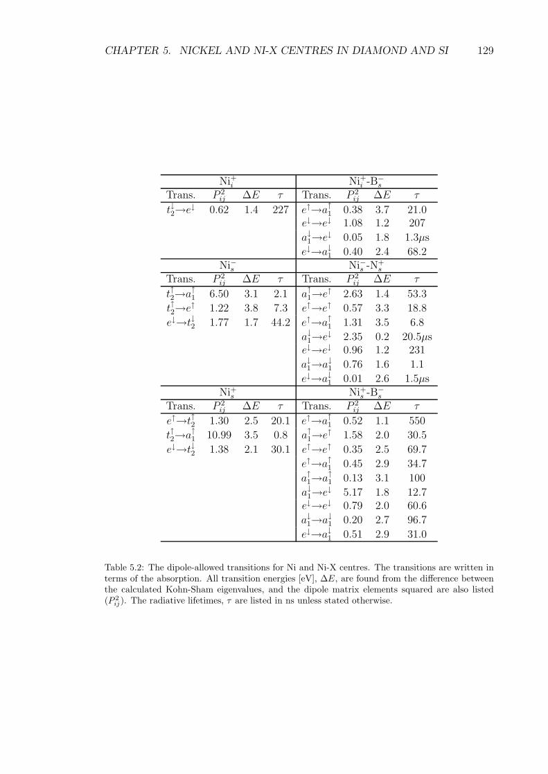
CHAPTER 5. NICKEL AND NI-X CENTRES IN DIAMOND AND SI 129
Ni+i Ni+i -B−s
Trans. P 2ij ∆E τ Trans. P 2
ij ∆E τ
t↓2→e↓ 0.62 1.4 227 e↑→a↑1 0.38 3.7 21.0e↓→e↓ 1.08 1.2 207
a↓1→e↓ 0.05 1.8 1.3µs
e↓→a↓1 0.40 2.4 68.2Ni−s Ni−s -N+
s
Trans. P 2ij ∆E τ Trans. P 2
ij ∆E τ
t↑2→a↑1 6.50 3.1 2.1 a↑1→e↑ 2.63 1.4 53.3
t↑2→e↑ 1.22 3.8 7.3 e↑→e↑ 0.57 3.3 18.8
e↓→t↓2 1.77 1.7 44.2 e↑→a↑1 1.31 3.5 6.8
a↓1→e↓ 2.35 0.2 20.5µse↓→e↓ 0.96 1.2 231
a↓1→a↓1 0.76 1.6 1.1
e↓→a↓1 0.01 2.6 1.5µsNi+s Ni+s -B−
s
Trans. P 2ij ∆E τ Trans. P 2
ij ∆E τ
e↑→t↑2 1.30 2.5 20.1 e↑→a↑1 0.52 1.1 550
t↑2→a↑1 10.99 3.5 0.8 a↑1→e↑ 1.58 2.0 30.5
e↓→t↓2 1.38 2.1 30.1 e↑→e↑ 0.35 2.5 69.7
e↑→a↑1 0.45 2.9 34.7
a↑1→a↑1 0.13 3.1 100
a↓1→e↓ 5.17 1.8 12.7e↓→e↓ 0.79 2.0 60.6
a↓1→a↓1 0.20 2.7 96.7
e↓→a↓1 0.51 2.9 31.0
Table 5.2: The dipole-allowed transitions for Ni and Ni-X centres. The transitions are written interms of the absorption. All transition energies [eV], ∆E, are found from the difference betweenthe calculated Kohn-Sham eigenvalues, and the dipole matrix elements squared are also listed(P 2
ij). The radiative lifetimes, τ are listed in ns unless stated otherwise.
CHAPTER 5. NICKEL AND NI-X CENTRES IN DIAMOND AND SI 130
dominant transition so that the others would then not be observed experimentally.
For each defect, the dominant transitions appear to be as follows:
• Ni+i The only dipole allowed transition is at 1.4 eV (t↓2 → e↓), and has an
estimated lifetime of 0.2 µs.
• Ni+i B−s The time dominant transition listed in Table 5.2 is at 3.7 eV. The
1.8 eV optical transition e→ a1 may account for the 1.40 eV centre, however,
the estimated transition time is 1.3 µs, and thus is unlikely to be seen since
there appear to be more rapid decay routes.
• Ni−s The dominant transitions appear to be from the t↑2 state to the conduction
band estimated at 2 ns. Now, the theory used does not describe the conduction
band well, so the interpretation of the rates has to be very careful. Thus it
is suggested that the dominant transition is t↑2 → conduction band, but the
e↓ → t↓2 transition is not ruled out.
• Ni−s N+s Again, the dominant transition is rather high in energy, so it is sug-
gested that the dominant observable transition would be the a↑1 → e↑ 1.4 eV
(53 ns) transition.
• Ni+s As before, the high energy (t↑2 → a↑1, 3.5 eV) transition is dominant, but
the e→ t2 transitions are in the 2-3 eV range and possess transition times of
around 20-30 ns.
• Ni+s B−s This defect possesses more dipole allowed transitions than any of the
others, but it is clear from the rates that the 1.8 eV, a↓1 → e↓ transition is
dominant with an estimated radiative lifetime of 13 ns.
5.1.6 Conclusions
To summarise, the conclusions are as follows:
1. It is clear from this work that Ni defects cause substantial movements to C
atoms lying beyond the Ni nearest neighbours. Erroneous results may occur
if these atoms are prevented from moving.
2. Ni+i is stable at the tetrahedral interstitial site with an effective spin of S = 12
and, in the absence of spin-orbit coupling, has no tendency to distort along
〈111〉, in contrast with previous calculations. Spin-orbit coupling promotes a
[111] distortion leading to a slight splitting of the e-level. The splitting would
be of the order of the splitting observed in the 1.40 eV optical defect, i.e.

CHAPTER 5. NICKEL AND NI-X CENTRES IN DIAMOND AND SI 131
around 2.7 meV. This would imply that the distortion would vanish above
30 K. The defect is a candidate for the NIRIM-1 defect observed in low N
diamonds, especially when B is present. NIRIM-1 is known the have Td sym-
metry above 25 K [148]. However, it is not the only candidate. The defect
results in an expansion of the cage of nearest neighbours by almost 10% which
might be observable by X-ray experiments. There is a mid-gap doublet e-level
with single hole lying ∼1.4 eV above a filled triplet t2 level. The transition
time between these levels is estimated to be 227 ns. Surprisingly, no optical
bands are correlated with the NIRIM-1 defect.
3. The Ni+i -B−s donor-acceptor complex has effective spin S = 1
2with trigonal
symmetry. The presence of B splits the fully occupied t2 level of Ni+i but
not the highest occupied e-level. The optical transition energies are then
similar to Ni+i (see Fig. 5.2). The a1 → e (2E → 2A1) 2.4 eV transition
which has a transition time estimated to be 68 ns could be responsible for the
1.40 eV optical centre. The transition should be split by the zero-point energy
of the two B isotopes present, assuming this to be resolvable. The ground
state would also be split by the spin-orbit interaction. The complex is a also
candidate for NIRIM-2; we note that the NIRIM-2 signal initially increases
with B, but apparently disappears for larger concentrations of B. This may
be because as the Fermi-level drops, Ni2+i defects may be created, but this
would then be seen as an S = 1 centre (which is estimated to be around
0.9 eV more stable than S = 0). Alternatively, a number of complexes could
form which lead to broad EPR signals. The absence of a hyperfine interaction
with 11B [153] may be due to the e-wavefunctions containing the hole having
a nodal surface that passes through the B site.
4. Ni−s is stable at a lattice site and the S = 32
configuration has an energy more
than 1 eV lower than that with S = 12. The C-Ni bond lengths are 1.86 A and
the t2 pseudo-wavefunctions overlap both Ni and its C neighbours. It possesses
a filled triplet t↑2 level around mid-gap, and a corresponding empty t↓2 level lies
about 1.4 eV above a filled e↓ level. The defect has been identified by EPR
experiments and associated with the 2.51 eV optical absorption band seen in
N rich diamonds defect [148]. Another transition at 1.883 eV is always found
along with the 2.51 eV line but the two have not been formally correlated.
The transition state calculation estimates 2.3 eV for the 4A2 → 4T2 optical
transition, which is fair agreement with experiment . We suspect that the
CNDO result which predicts a spin S = 12
configuration, a21t
12, is due to an
incorrect parameterisation used to describe the interaction of the Ni atom
CHAPTER 5. NICKEL AND NI-X CENTRES IN DIAMOND AND SI 132
with the surrounding diamond lattice. This in turn leads to the rogue a1-level
lying below the t2-level.
5. The donor-acceptor complex, Ni−s -N+s (S = 1
2), is found to be stable with C3v
symmetry. It possesses a hole in a mid-gap e↑ level about 1.4 eV above a filled
a↑1 level. This would explain the 1.693 eV transition observed in Ref. [163]
and attributed to Ni-N defects. We note there would be a correlation between
the loss of Ni+s centres and the growth of the 1.693 eV system, assuming that
the only sinks for N+s are the Ni−s defects. There would be no correlation
expected, and none found, with the density of neutral Ns defects. The latter
are related to the strength of the lattice absorption at 1330 cm−1.
6. Ni+s (S = 12) lies close to the Td lattice site and possesses two optical transitions
around 2 eV, and one around 3.5 eV. The symmetry and spin state are also
consistent with the NIRIM-1 centre. Ni2+s would empty the t2 level altogether,
and thus be EPR-inactive (S=0).
7. The Ni+s -B−s (S = 1
2) defect has trigonal symmetry and a 2E ground state. The
complex gives rise to a large number of optical transitions and is a candidate
for NIRIM-2 and the 1.40 eV zero phonon doublet defect.
8. The high symmetry of isolated interstitial and substitutional impurities leads
to a number of degenerate gap levels, and in practice (depending on the charge
state), these will be split into multiplets. If the multiplet splittings are of order
0.5 eV [93] then each defect will give a small number of optical transitions
broadened by this amount. However, if the negative and positive charge states
are adopted for the substitutional and interstitial impurities respectively, then
the ground states are well defined (4A2 and 2E). Conserving spin gives well
defined excited states (4T2 and 2T2). It is interesting to note that these results
suggest that Ni0i would be electrically and optically inactive. Other charge
states are generally more complex. For example, Ni0s would have a ground
state arising from the e4t22 electronic configuration which leads to T2 ⊗ T2
multiplets (the same a the neutral vacancy - Sec. 4.2) which could conceivably
have an internal transition.
9. In general, when Nii and Nis are complexed with other impurities, the gap
states split to produce a larger number of possible transitions at smaller ener-
gies. Table 5.2 shows that one would expect at least 20 absorption lines from
the 6 defects studied. However, experiment has only identified a small num-
ber, about 68, of optical lines associated with Ni, which suggests that either81.22, 1.40, 1.883, 2.51, 2.56, and 3.1 eV

CHAPTER 5. NICKEL AND NI-X CENTRES IN DIAMOND AND SI 133
only a small number of complexes exist, the optical transitions possess small
oscillator strengths, there is a dominant transition mechanism for each defect
type, or the transitions are hidden by other absorption. This is especially
true at higher energies, say ∼ 3.5 eV, where Ni related peaks are buried in
the nitrogen absorption band. Using the crude estimate for transition times
indicated in the text, it would appear that a dominant transition mechanism
occurs for each defect, and this could account for the small number of observed
Ni-related optical centres.
10. As the only defect for which there is convincing evidence is Ni−s , one wonders
whether all the Ni related optical and EPR defects are simply different charge
states of substitutional Ni possibly complexed with other impurities. Further-
more, if Ni was found at interstitial site, one would expect Ni2+i (S = 1) to
be seen under EPR, and to date this is not the case. However, Ni2+s would
have zero effective spin, and would therefore not generate an EPR signal.
Hence, we suggest that NIRIM-1 and NIRIM-2 may be Ni+s and Ni+s -B−s com-
plexes respectively. It is noteworthy that all the optical features due to Ni
are confined to octahedral growth sectors of diamond [159] and this also sug-
gests that the centres are incorporated as substitutional defects at the growing
(111) surfaces.
11. An alternative acceptor to those reported here is the vacancy in analogy to the
complexes with P, N and Si substitutional impurities. Preliminary studies into
this system strongly suggest that the structure would possess theD3d structure
preferred by the Si and P impurities, but due to problems in obtaining a self-
consistent charge density for Ni-V, no detailed results will be presented here.
This is an on-going area of study.
5.2 Nickel and nickel-hydrogen complexes in Si
5.2.1 Introduction
As stated above in Sec. 5.1.3, the vacancy model of substitutional TM-impurities
on the far-right of the periodic table [151, 181], considers that the d levels of the
TM impurity lie deep in the valence band of Si and couple weakly with the t2 levels
arising from the Td symmetry of the ideal vacancy. The important implication is
then that the gap-levels and structure of the defect are largely determined by those
of a perturbed vacancy [152, 169, 170, 171]. For Pt−, Pd− and Ni−, the gap t2 levels
contain three electrons and according to the Jahn-Teller theorem, a distortion will
occur for an S=1/2 state, leading to a splitting of these levels and a lowering of
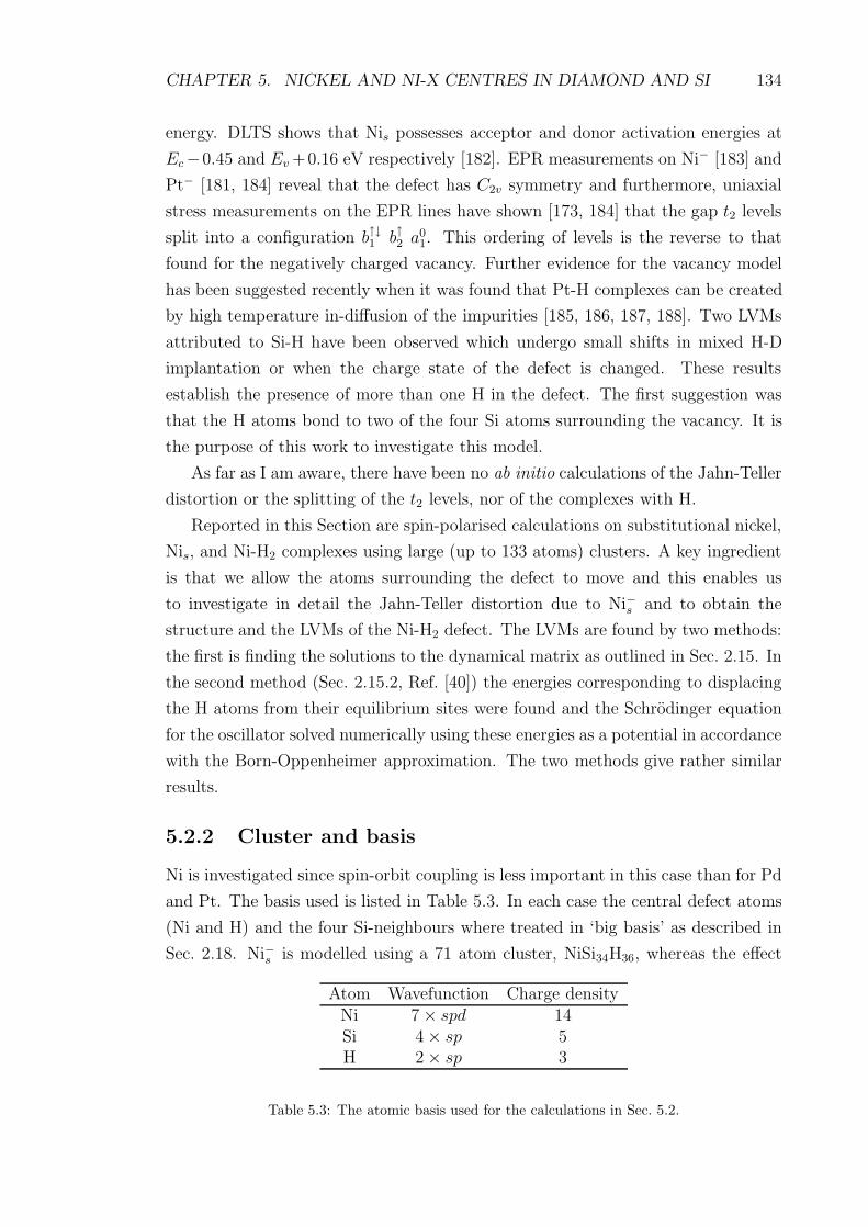
CHAPTER 5. NICKEL AND NI-X CENTRES IN DIAMOND AND SI 134
energy. DLTS shows that Nis possesses acceptor and donor activation energies at
Ec−0.45 and Ev +0.16 eV respectively [182]. EPR measurements on Ni− [183] and
Pt− [181, 184] reveal that the defect has C2v symmetry and furthermore, uniaxial
stress measurements on the EPR lines have shown [173, 184] that the gap t2 levels
split into a configuration b↑↓1 b↑2 a01. This ordering of levels is the reverse to that
found for the negatively charged vacancy. Further evidence for the vacancy model
has been suggested recently when it was found that Pt-H complexes can be created
by high temperature in-diffusion of the impurities [185, 186, 187, 188]. Two LVMs
attributed to Si-H have been observed which undergo small shifts in mixed H-D
implantation or when the charge state of the defect is changed. These results
establish the presence of more than one H in the defect. The first suggestion was
that the H atoms bond to two of the four Si atoms surrounding the vacancy. It is
the purpose of this work to investigate this model.
As far as I am aware, there have been no ab initio calculations of the Jahn-Teller
distortion or the splitting of the t2 levels, nor of the complexes with H.
Reported in this Section are spin-polarised calculations on substitutional nickel,
Nis, and Ni-H2 complexes using large (up to 133 atoms) clusters. A key ingredient
is that we allow the atoms surrounding the defect to move and this enables us
to investigate in detail the Jahn-Teller distortion due to Ni−s and to obtain the
structure and the LVMs of the Ni-H2 defect. The LVMs are found by two methods:
the first is finding the solutions to the dynamical matrix as outlined in Sec. 2.15. In
the second method (Sec. 2.15.2, Ref. [40]) the energies corresponding to displacing
the H atoms from their equilibrium sites were found and the Schrodinger equation
for the oscillator solved numerically using these energies as a potential in accordance
with the Born-Oppenheimer approximation. The two methods give rather similar
results.
5.2.2 Cluster and basis
Ni is investigated since spin-orbit coupling is less important in this case than for Pd
and Pt. The basis used is listed in Table 5.3. In each case the central defect atoms
(Ni and H) and the four Si-neighbours where treated in ‘big basis’ as described in
Sec. 2.18. Ni−s is modelled using a 71 atom cluster, NiSi34H36, whereas the effect
Atom Wavefunction Charge densityNi 7 × spd 14Si 4 × sp 5H 2 × sp 3
Table 5.3: The atomic basis used for the calculations in Sec. 5.2.

CHAPTER 5. NICKEL AND NI-X CENTRES IN DIAMOND AND SI 135
of H was investigated in a 133 atom, negatively charged cluster NiSi70H62 where 19
central atoms were relaxed.
5.2.3 Results
The Ni atom was placed along [100] so that the symmetry of the cluster is C2v.
Three close-by levels for each spin lay in the gap region and these are occupied
with three electrons according to Fermi-statistics corresponding to 0 K, i.e. the
lowest was filled, the next filled in the up-spin case only and the others were empty.
The self-consistent energy and forces acting on the central 17 atoms were then
found for this S = 1/2 configuration, and these atoms were allowed to move to
minimise the energy of the cluster. The Ni atom moved closer to the substitutional
site while the surrounding Si atoms moved outwards from their lattice positions.
The splitting between the t2-derived levels gradually decreased and eventually we
were unable to obtain a self-consistent solution. This arises because during the
course to self-consistency, the three close-by gap levels, the uppermost of which is
empty, cross over and if, for example, the a1 state falls below the b1 state, the charge
density and hence potential changes discontinuously. On the next iteration, the level
ordering often reverses and the process never converges. This problem of ‘charge
sloshing’ is well-known and often occurs for close-by levels. It can be overcome by
occupying the gap-levels with Fermi-statistics corresponding to a finite temperature
(as described in Sec. 2.13.1) larger than the splitting of the t2 levels. This spreads
out the electrons among the three gap levels and the discontinuity in the charge
density arising from cross-over is reduced. However, this almost eliminates the
Jahn-Teller driving force for the Ni atom to lie off-site. For the finite-temperature
calculation the lowest energy configuration corresponded to a structure where the
Ni atom is essentially on site but the four surrounding Si atoms were displaced
outwards from their lattice sites by 0.270 A and two of them were further displaced
along [100] by 0.006 A. Second shell Si atoms were displaced by ∼ 0.07 A. The three
gap levels were split by only 5 meV and the highest occupied spin-up level was 0.6 eV
below the corresponding (but empty) spin-down level. Thus the departure from Td
symmetry is extremely small. The ordering of the t2-derived gap levels is b↑↓1 b↑2 a01
is the same as that found experimentally.
The problem of obtaining self-consistent solutions can now be overcome by re-
stricting the electronic configuration to be b↑↓1 b↑2 a01. Then during the passage to
self-consistency, there is no discontinuity in the charge density but the energy levels
that are occupied at each stage are not necessarily in ascending order. However,
towards the end of the self-consistency cycle the energy levels ordered correctly and
the final energy obtained was lower than that obtained by the imposition of a tem-

CHAPTER 5. NICKEL AND NI-X CENTRES IN DIAMOND AND SI 136
perature. The Ni atom was then moved along [100] and the equilibrium structure
was found to correspond to a displacement of 0.13 A from the lattice site. The two
Si atoms with Cartesian components along [100] were displaced almost radially by
(0.15, ± 0.25, ± 0.22) A and moved away from each other, whereas the other two Si
atoms with components along [100] were displaced (-0.07,± 0.16, ∓ 0.13) A so that
they approached each other. Curiously, the four Ni-Si bonds are almost identical
in length at 2.645 A. This distortion is similar to that found experimentally for the
negatively charged vacancy [172].
Suppose now, we occupy the t2 derived states according to a↑↓1 b↑1 b02. This is the
configuration found experimentally for the negatively charged vacancy [172] but not
for Ni−s . Then the self-consistent cluster energy is higher than the previous config-
uration by 17 meV. We note that although we have shown that the C2v distortion
has a lower energy than Td it leaves open the possibility that other symmetries, e.g.
D2, have even lower energies as suggested in Ref. [189]. The slight distortion from
Td to C2v symmetry is consistent with the ease of reorientation of Pt around the
central lattice site. This motion occurs for temperatures above 12 K or even when
the slightest stress is imposed on the crystal at 2 K [184].
The pseudo-wave function of the t2-derived levels all possess a nodal surface
lying between the TM impurity and the surrounding Si atoms and peaks on either
side of the Si atoms along 〈111〉. This suggests that H atoms will lie either between
Si and Ni in the configuration suggested previously [173, 185, 187, 188], or outside
at anti-bonding (AB) sites as shown in Fig. 5.5. There were no problems with
self-consistency in the present case. For the first defect where the H atoms are
within the ‘vacancy’ occupied by the Ni atom, the H atoms repelled Ni along [100]
from its lattice site by 0.20 A and formed Si-H bonds of length 1.508 A with a
H-H separation of 1.517 A. The LVMs due to H were calculated to lie at 2477 and
2511 cm−1. These values are far from the experimental ones for PtH2 [173, 185, 186]
and strongly suggest that this model is incorrect. The strong coupling between the
H atoms occurs because there is so little room for both Ni and H within the vacancy.
The second defect (Fig. 5.5) when relaxed yielded an energy 0.08 eV below the first
structure and the Ni atom moved 0.3 A along [100] towards the H atoms and the
Si-H lengths became 1.557 A. The separation between the H atoms was 7.3 A. The
vibrational modes are given in Table 5.4. The two H related modes are slightly
split, by 7 cm−1, with the higher mode being A1. Now, uniaxial stress splitting
experiments on PtH2 [186] show that the upper and lower modes also have A1 and
B1 symmetries respectively. The stretch modes are close to those reported for PtH2
but the bend modes have not yet been detected.
Anharmonic effects are known to be important for H modes (Sec. 6.2, Refs. [40,

CHAPTER 5. NICKEL AND NI-X CENTRES IN DIAMOND AND SI 137
Figure 5.5: Ni-H2 Complex with H at anti-bonding (AB) sites.
54, 56]) and we investigated their influence in the following way: the two modes
at 2009.9 and 2003.2 cm−1 represent A1 and B1 vibrational modes in which the H
atoms move either in phase or out of phase with each other. The energies necessary
to displace the H atoms by an amount r, parallel to the Si-H bonds, were evaluated
for each of these modes. This energy contains only even powers of r in the B1 mode
whereas it contains both even and odd powers in the A1 mode. The Schrodinger
equation for the oscillator was solved numerically [40] and the A1 and B1 frequencies
were then found to be 2037 and 2060 cm−1 and are separated by 23 cm−1. However,
now the B1 mode lies above the A1 mode contrary to experiment. Thus even though
the separation of the H atoms is very large, 7.3 A, the two modes are split and their
ordering reversed by these anharmonic effects by an amount twice as large as that
observed for Pt-H2. However, there are other anharmonic terms which should be
considered. For example, r1θ21 + r2θ
22 terms where rk and θk are the changes in the
equilibrium Sik-Hk lengths and angles respectively. These mix the stretch and bend
modes and are only present in the A1 mode where r1 = r2. These have the effect of
decreasing the mean Si-H length hence pushing up the A1 frequency. Such a term
then might well displace the A1 mode above that of B1.
Several other models of the defect were investigated, but all gave energies above
that of the AB structure. In addition, their vibrational modes were far from the
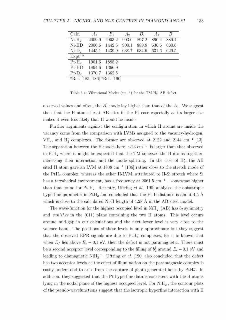
CHAPTER 5. NICKEL AND NI-X CENTRES IN DIAMOND AND SI 138
Calc. A1 B1 A2 B2 A1 B1
Ni-H2 2009.9 2003.2 903.0 897.2 890.4 889.4Ni-HD 2006.6 1442.5 900.1 889.8 636.6 630.6Ni-D2 1445.1 1439.9 638.7 634.6 631.6 629.5Expta,b
Pt-H2 1901.6 1888.2Pt-HD 1894.6 1366.9Pt-D2 1370.7 1362.5aRef. [185, 186] bRef. [190]
Table 5.4: Vibrational Modes (cm−1) for the TM-H−2 AB defect
observed values and often, the B1 mode lay higher than that of the A1. We suggest
then that the H atoms lie at AB sites in the Pt case especially as its larger size
makes it even less likely that H would lie inside.
Further arguments against the configuration in which H atoms are inside the
vacancy come from the comparison with LVMs assigned to the vacancy-hydrogen,
VH2, and H∗2 complexes. The former are observed at 2122 and 2144 cm−1 [13].
The separation between the H modes here, ∼23 cm−1, is larger than that observed
in PtH2 where it might be expected that the TM squeezes the H atoms together,
increasing their interaction and the mode splitting. In the case of H∗2, the AB
sited H atom gave an LVM at 1838 cm−1 [136] rather close to the stretch mode of
the PtH2 complex, whereas the other H-LVM, attributed to H-Si stretch where Si
has a tetrahedral environment, has a frequency at 2061.5 cm−1 – somewhat higher
than that found for Pt-H2. Recently, Uftring et al. [190] analysed the anisotropic
hyperfine parameter in PtH2 and concluded that the Pt-H distance is about 4.5 A
which is close to the calculated Ni-H length of 4.28 A in the AB sited model.
The wave-function for the highest occupied level in NiH−2 (AB) has b2 symmetry
and vanishes in the (011) plane containing the two H atoms. This level occurs
around mid-gap in our calculations and the next lower level is very close to the
valence band. The positions of these levels is only approximate but they suggest
that the observed EPR signals are due to PtH−2 complexes, for it is known that
when Ef lies above Ec − 0.1 eV, then the defect is not paramagnetic. There must
be a second acceptor level corresponding to the filling of b↓2 around Ec − 0.1 eV and
leading to diamagnetic NiH−−2 . Uftring et al. [190] also concluded that the defect
has two acceptor levels as the effect of illumination on the paramagnetic complex is
easily understood to arise from the capture of photo-generated holes by PtH−2 . In
addition, they suggested that the Pt hyperfine data is consistent with the H atoms
lying in the nodal plane of the highest occupied level. For NiH−2 , the contour plots
of the pseudo-wavefunctions suggest that the isotropic hyperfine interaction with H

CHAPTER 5. NICKEL AND NI-X CENTRES IN DIAMOND AND SI 139
would vanish leaving only an anisotropic one. However, spin-polarisation causes a
difference in all the spin-up and spin-down valence wave-functions and results in a
small polarised charge density of -0.007 a.u. at each proton. This is only -2% of the
charge density of a H atom in vacuo. Its magnitude is within a factor of three found
experimentally for PtH2 [173, 185, 186, 188]. It is unclear whether this discrepancy
is due to calculational errors or differences between Ni and Pt.
5.2.4 Conclusions
In conclusion, the calculations show that the substitutional Ni− defect with Td
symmetry is unstable against a displacement along the 〈100〉 axis. The t2 gap level
is split into b1, b2 and a1 levels in ascending energy. Nis can complex with two
H atoms at AB sites and act as a double acceptor. It gives two H-LVMs around
2000 cm−1. The polarisation charge density is very small and negative at the H
nuclei and we suggest that PtH2 complexes assume the same structure.

Chapter 6
Carbon-Hydrogen complexes inGaAs.
‘The great tragedy of Science: the slaying of a beautiful hypothesis by
an ugly fact.’
Thomas Huxley
6.1 Introduction
Carbon is a very important dopant in GaAs due to its low diffusivity and high
solubility. In this Chapter, the details of the interaction of substitutional CAs
with hydrogen is explored in the cases of the isolated CAs-H complex and a class
of complexes due to CAs-dimers. The former case has been the subject of much
experimental and theoretical work, but the emphasis in Sec. 6.2 is the anharmonic
nature of the LVM observed experimentally at 2635 cm−1.
A number of C-H stretch modes have been observed at frequencies higher than
that due to CAs-H, a number of which exhibit a strong polarisation in one of the
〈110〉 directions. This is believed to be a consequence of the manner C is incorpo-
rated during growth, and the available experimental data points toward CAs dimer
complexing with H. The structures and modes of a range of possible configurations
are presented in Sec. 6.3.
6.2 Anharmonic theory of the CAs-H complex.
6.2.1 Introduction.
As discussed in Sec. 2.15.2, anharmonicity is especially important for vibrations
where the amplitude is large (typically > 0.1 A). Thus, anharmonic effects have
140

CHAPTER 6. CARBON-HYDROGEN COMPLEXES IN GAAS. 141
become evident experimentally where hydrogen is involved [54, 56], and in par-
ticular the high frequency stretch mode of the CAs-H complex in GaAs [51]. As
discussed in Sec. 2.15.2, CAs-H in GaAs exhibits an anomalous isotope shift, and
Davidson et al. found that the anharmonic vibration is characterised by the param-
eters χ = 1.1 and B = 176 amu cm−1. Now, absorption due to the overtone of a
mode is made possible by anharmonicity, but despite the large anharmonicity of the
2635 cm−1 mode, no overtone has been reported. An overtone has been observed for
the C-H vibration of the HCN molecule which has an anharmonicity parameter of
Bo=102 amu cm−1 [191]. This is only 58% of the value of B for the stretch mode in
GaAs. These experimental results raise the question as to why the anharmonicity
is so large for CAs-H in GaAs and yet the intensity of the overtone seems to be so
low. The aim of this section is to provide a possible answer.
The theory is applied to HCN in Sec. 6.2.4 and to CAs-H in GaAs in Sec. 6.2.5.
In Sec. 6.2.6 the effects of electrical anharmonicity are considered. First, a brief
review of carbon and carbon-hydrogen complexes in GaAs is presented.
6.2.2 Experimental background & previous theoretical stud-
ies.
Carbon is known to preferentially substitute for As in GaAs [192]. Its low diffusiv-
ity [193, 194, 195] and high solubility make it an ideal dopant. Acceptor concentra-
tions of the order of 1020 cm−3 and higher have been achieved in molecular beam
epitaxy (MBE) [196], metalorganic MBE (MOMBE) [193, 194, 197, 198, 199], and
metalorganic vapour phase epitaxy (MOVPE) [200, 201, 202]. However hydrogen
introduced during growth leads to a degradation in electrically activity: it can lead
to premature device failure [203, 204], and passivate up to 60% of CAs [205].
The hydrogen passivation of single carbon acceptors to form CAsH pairs was
first reported by Pan et al. [206], and the 2635 cm−1 infrared absorption band has
been assigned to the H-stretch mode of this centre [207]. The isotopic shifts arising
from 13C (Ref. [207]) and D (Ref. [208]) unambiguously identify the constituent
chemical species, and uniaxial stress studies indicate that H lies along a trigonal
axis [207]. Previous theoretical studies have shown that the lowest energy atomic
configuration in the neutral charge state is the hydrogen atom sited near a C-Ga
bond-centre, as shown in Fig. 6.1 [45, 209].
As well as the intense infra-red absorption due to the C-H stretch mode, a
complete set of lower lying vibrational modes have been observed experimentally for
CAs-H. Infra-red spectroscopy on GaAs containing high concentrations of C and H
grown by MBE and CVD revealed modes at 453 (labelled X) and 563 cm−1 (labelled
Y) [199]. Both were subsequently shown to be due to CAs-H as they exhibited shifts

CHAPTER 6. CARBON-HYDROGEN COMPLEXES IN GAAS. 142
As
HC
[111]
GaAs
As
Ga
Ga
Ga
Figure 6.1: The CAs-H defect in GaAs.
with 13C and D. A Raman scattering experiment [210, 211] assigned the 453 cm−1
band to the C-related A1-band. Y is now believed to be the E+ band [51]. The E−
band was not observed in the early experiments. However, in deuterated samples,
the E− band was detected at 637 cm−1. This must imply that the unobserved
H-related E−-band lies above 637 cm−1 and a simple force constant model [51]
predicted the band to lie at 745.2 cm−1. The failure of the infra-red experiments to
locate this band was explained by the ab initio theory as the consequence of a small
transition dipole moment [212]. This band has since been detected at 739 cm−1 by
Raman scattering experiments [70].
The early calculations [45, 213] performed using AIMPRO predicted the high
frequency, stretch modes of CAs-H in good agreement with experiment, but rep-
resented the low frequency, bend-modes rather poorly. The basis used in these
calculations was rather modest, and when the basis was increased (Ref. [214]), the
modes at low frequency were much better reproduced. However, the stretch modes
became much higher in frequency, overestimating by more than 300 cm−1. I shall
show in Sec. 6.2 that this discrepancy can, at least in part, be mitigated by the
inclusion of anharmonic terms in the calculation of the vibrational mode.
The CAs-H complex has also been treated in a plane wave basis, super-cell
approach [209]. The calculation produced C-H and C-Ga lengths of 1.2 A and
2.0 A respectively, and vibrational modes of 2781 and 724 cm−1 for the C-H stretch
and E− modes respectively, although the lower modes were not reported.

CHAPTER 6. CARBON-HYDROGEN COMPLEXES IN GAAS. 143
CAs-H HCNAtom Wavefunction Charge Atom Wavefunction Charge
density densityGa 8 × sp 8 H 2 × sp 3As 8 × sp 8 C 6 × sp 6C 8 × sp 8 N 8 × sp 8H 2 × sp 3 Bond-centres 1 × sp 1
Bond-centres 1 × sp 1
Table 6.1: The atomic basis used for the calculations in Sec. 6.2.
Bond-lengthsBond Calc ExptH-C 1.07 1.06C-N 1.15 1.15
Vibrational modes12C-H 12C-D
Calc Expt Calc Expt3318.9 3312 2611.5 26292125.0 2089 1944.5 1906764.3 712 609.1 569
Table 6.2: The calculated and experimental [191] structure (A) and vibrational modes (cm−1) ofthe HCN molecule.
6.2.3 Clusters and basis.
The basic theory and approach used to estimate the effects of anharmonicity are
detailed in Sec. 2.15.2. The cluster used in all the following calculations on the
anharmonicity of the C-H stretch mode is bond-centred, and has 87-atoms: (CH)-
Ga22As21H42. The basis adopted for each of the atomic species are listed in Ta-
ble 6.1.
For CAs-H, the central C and H atom, as well as the four surrounding Ga atoms
were treated in big basis, as defined in Sec. 2.18. The remaining atoms were treated
using a minimal basis. A single bond-centre was placed between all neighbouring
atoms, except where one of these atoms was H. For HCN, all atoms were in big
basis, and a bond centre was placed in each bond.
The quasi-harmonic vibrational modes were calculated as described in Sec. 2.15,
where for CAs-H, energy double derivatives were found between each of the big-basis
atoms, and the remaining atoms treated using the Musgrave-Pople valence force
potential. Naturally, for HCN, all the double derivatives were computed.
6.2.4 Prussic acid molecule: HCN
The calculated structure and quasi harmonic LVMs are listed in Table 6.2. The
agreement with the experimental values [191] is excellent.
The values of the double derivatives calculated for HCN are listed in Table 6.3,

CHAPTER 6. CARBON-HYDROGEN COMPLEXES IN GAAS. 144
EC,C EC,H EH,H
1.565 -0.374 0.376
Table 6.3: Calculated energy double derivatives for HCN (a.u.).
-0.25 0.00 0.25 0.50 0.75
0.00
0.02
0.04
0.06
0.08
0.10
(a)
(b)
(c)
(d)
Figure 6.2: (a) Potential energy (au) versus displacement from equilibrium, x, (au) for C-H stretchin HCN. The oscillator wavefunctions for the ground (b), first (c) and second (d) excited statesare also shown. The horizontal lines show the energies of these states.
which show that EC,C is rather large. In particular, EC,C/EH,H=4.2, which is the
same order of magnitude as MC/MH . This satisfies the conditions for a physical
value of χ < 1 (Sec. 2.15.2.4). Inserting the double derivatives from Table 6.3
into Eq. 2.44 and iterating provides a value of χ = 0.77 for H and χ = 0.59 for
D. Evaluating the quasi-harmonic frequencies instead from the expression ν2 =
EH,H(1/mH +1/χmC) gives values of 3305 and 2512 cm−1 for H and D respectively.
Hence, the neglect of motion of the N atom is valid in the case of H since this
frequency is very close to that derived from diagonalising the dynamical matrix.
This is not the case for D, due to the coupling between the C-D and N-C modes.
The anharmonic potential is calculated as prescribed in Sec. 2.15.2, where the
motion of the N atom is neglected. Note, if the N atom is allowed to relax at each
point in the vibronic potential, little change is observed. The potential is shown in
Fig. 6.2, along with the polynomial fit f(x) =∑8
n=2 anxn. The maximum error in
the fit, |f(x) − Eai(x)| where Eai(x) is the ab initio energy at a displacement x, is
7×10⁻⁵ a.u. (=16 cm−1). The coefficients of the fit are given in Table 6.4.
Equating a2 with k/2 and setting χ = 0.77 gives a harmonic frequency of
3552.5 cm−1. This is much higher than the quasi-harmonic and experimental val-
ues because higher order even terms in displacement are present in quasi-harmonic

CHAPTER 6. CARBON-HYDROGEN COMPLEXES IN GAAS. 145
a2 a3 a4 a5 a6 a7 a8
0.1846 -0.1932 0.1473 -0.0780 0.0234 -0.0265 0.0210
Table 6.4: Calculated polynomial coefficients (a.u.) for the fit to the vibronic potential of HCN.
modes, which tend to reduce them. Also plotted in Fig. 6.2 are the lowest three
energy levels and their wavefunctions as calculated using the secular equation de-
scribed in Sec. 2.15.2. Two features are worthy of note. First, the wavefunction
amplitudes are essentially zero outside of the range of energies calculated for the
vibration. If this were not the case, then the fit to the potential might be unreliable
in a region important to the vibration, and hence the wrong frequencies would be
found. Secondly, the amplitude of the peaks are larger for positive x than negative
x, due to the repulsive nature of the C-N bond. This asymmetry is important when
considering the electrical anharmonicity.
The calculated anharmonic modes are listed in Table 6.5. They are some 4%
lower than experiment, but the anharmonicity parameter, A is in good agreement.
Note, A is little changed by neglecting χ, despite the absolute value of the frequency
changing by 34 cm−1.
Mode χ = 0.77 χ = 1.0 Observed a5−8=0 x4 fitFundamental 3189 3155 3312 3229.7 1947.2Overtone 6273 6206 6521.7 6448.2 4006.6Anharmonicity, A 105 104 102.3 11.2 -112.2
Table 6.5: Calculated and observed anharmonic C-H frequencies (cm−1) of the HCN molecule.
The primary source of error in the vibrational frequencies comes from the pre-
cision with which theory can predict bond-lengths. The bond-length can effectively
be changed by adding a linear term to the potential energy (Sec. 2.15.2). If, using
this method, the C-H bond is decreased from the calculated 1.07 A to 1.06 A the
vibrational modes are almost coincident with experiment. A plot showing how the
vibrational modes vary with effective bond-length is shown in Fig. 6.3. Note, the
anharmonicity does not significantly change, showing that this parameter is only
weakly dependent on bond-length. A similar treatment for the DCN system is
hampered by the coupling between D-C and C-N modes.
It is instructive to compare these results with those of lowest order perturbation
theory. In order to do this, we must have a potential with only up to cubic and
quartic terms in x. This can be achieved in one of two ways. First, one might set
the coefficients ai, i=5,6,7,8 all equal to zero. This resultant frequencies are shown
alongside the experimental values in Table 6.5, and are in very poor agreement.

CHAPTER 6. CARBON-HYDROGEN COMPLEXES IN GAAS. 146
-0.03 -0.02 -0.01 0.00 0.01
3000
4000
5000
6000
7000
(a)
(b)(c)
Figure 6.3: The variation of the fundamental (a) and overtone (b) frequencies in cm−1 with thechange in the equilibrium C-H length (A) in HCN. Curve (c) shows the the fundamental frequency×2 and its difference from (b) demonstrates that the anharmonicity varies slowly with the C-Hlength. The horizontal lines show the experimental frequencies (3312 and 6521.7 cm−1) [191]).
The alternative is to fit a quartic potential. The maximum error in the fit is much
greater than before (7.8×10⁻³ a.u. (1711cm−1), and consequentially the vibrational
modes are very poor. These are also shown in Table 6.5, where it can be seen that
the anharmonicity parameter is even the wrong sign. This is clear evidence that
such a procedure is insufficient to describe these vibrations.
In summary, using the relatively simple example of the tri-atomic molecule, it
has been shown that the anharmonic treatment described in Sec. 2.15.2 can describe
both the absolute frequencies and the anharmonicities of di-atomic vibrations. The
anharmonicity parameter, A, is relatively insensitive to bond-length and mass. Sig-
nificantly, low order perturbation theory is insufficient to model these systems.
6.2.5 The CAs-H stretch mode
The 87 atom bond-centred GaAs cluster with C at the central As site, and H placed
close to the centre of the C-Ga bond, was fully relaxed. The equilibrium C-H and
H-Ga lengths were 1.126 and 2.253 A respectively. The calculated energy double
derivatives are listed in Table 6.6, and the quasi-harmonic modes calculated by
diagonalising the dynamical matrix made up from these and valence force potential
terms are listed in Table 6.7.
Notice that the stretch mode is in poor agreement with experiment (11% error),
but that the lower lying, C-related modes are much more accurate.
If one uses Eq. 2.38 to derive a value for χ using the experimental values of
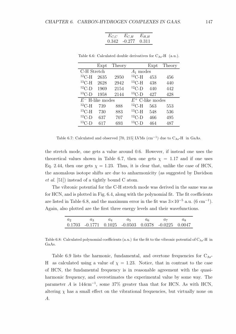
CHAPTER 6. CARBON-HYDROGEN COMPLEXES IN GAAS. 147
EC,C EC,H EH,H
0.342 -0.277 0.311
Table 6.6: Calculated double derivatives for CAs-H (a.u.).
Expt Theory Expt TheoryC-H Stretch A1 modes12C-H 2635 2950 12C-H 453 45613C-H 2628 2942 13C-H 438 44012C-D 1969 2154 12C-D 440 44213C-D 1958 2144 13C-D 427 428E− H-like modes E+ C-like modes12C-H 739 888 12C-H 563 55313C-H 730 883 13C-H 548 53612C-D 637 707 12C-D 466 49513C-D 617 693 13C-D 464 487
Table 6.7: Calculated and observed [70, 215] LVMs (cm−1) due to CAs-H in GaAs.
the stretch mode, one gets a value around 0.6. However, if instead one uses the
theoretical values shown in Table 6.7, then one gets χ = 1.17 and if one uses
Eq. 2.44, then one gets χ = 1.23. Thus, it is clear that, unlike the case of HCN,
the anomalous isotope shifts are due to anharmonicity (as suggested by Davidson
et al. [51]) instead of a tightly bound C atom.
The vibronic potential for the C-H stretch mode was derived in the same was as
for HCN, and is plotted in Fig. 6.4, along with the polynomial fit. The fit coefficients
are listed in Table 6.8, and the maximum error in the fit was 3×10⁻⁵ a.u. (6 cm−1).
Again, also plotted are the first three energy levels and their wavefunctions.
a2 a3 a4 a5 a6 a7 a8
0.1703 -0.1771 0.1025 -0.0503 0.0378 -0.0225 0.0047
Table 6.8: Calculated polynomial coefficients (a.u.) for the fit to the vibronic potential of CAs-H inGaAs.
Table 6.9 lists the harmonic, fundamental, and overtone frequencies for CAs-
H as calculated using a value of χ = 1.23. Notice, that in contrast to the case
of HCN, the fundamental frequency is in reasonable agreement with the quasi-
harmonic frequency, and overestimates the experimental value by some way. The
parameter A is 144cm−1, some 37% greater than that for HCN. As with HCN,
altering χ has a small effect on the vibrational frequencies, but virtually none on
A.
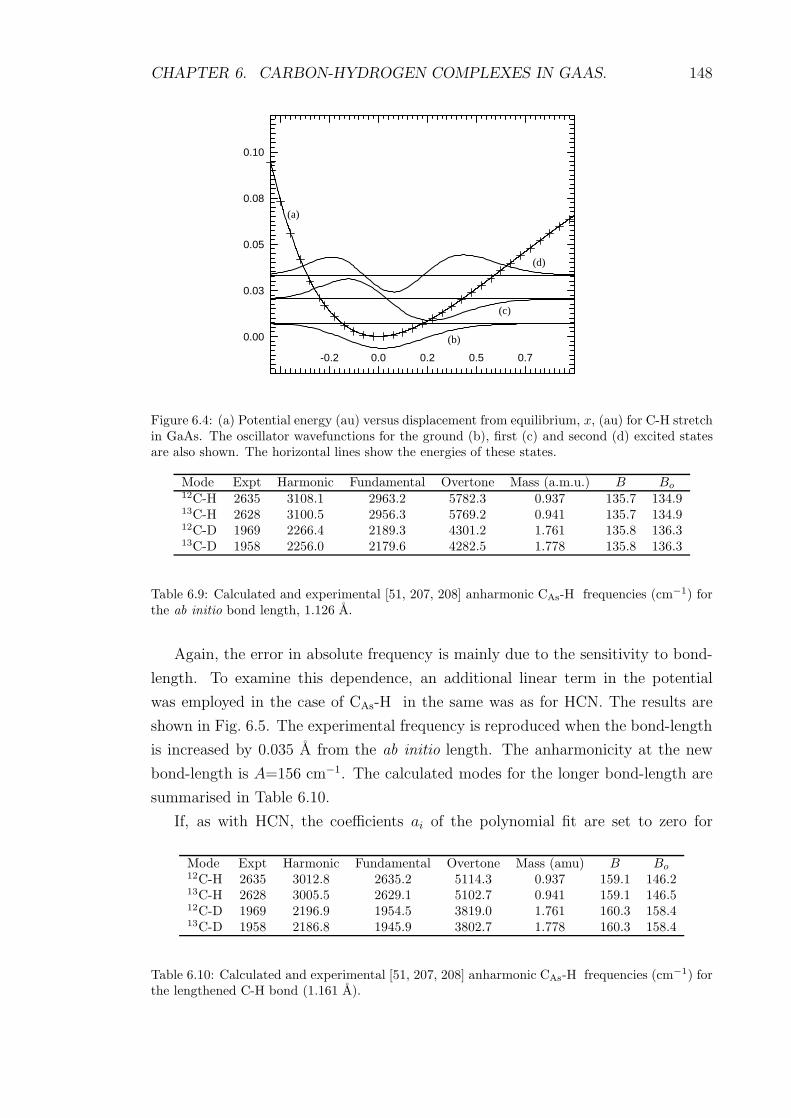
CHAPTER 6. CARBON-HYDROGEN COMPLEXES IN GAAS. 148
-0.2 0.0 0.2 0.5 0.7
0.00
0.03
0.05
0.08
0.10
(a)
(b)
(c)
(d)
Figure 6.4: (a) Potential energy (au) versus displacement from equilibrium, x, (au) for C-H stretchin GaAs. The oscillator wavefunctions for the ground (b), first (c) and second (d) excited statesare also shown. The horizontal lines show the energies of these states.
Mode Expt Harmonic Fundamental Overtone Mass (a.m.u.) B Bo12C-H 2635 3108.1 2963.2 5782.3 0.937 135.7 134.913C-H 2628 3100.5 2956.3 5769.2 0.941 135.7 134.912C-D 1969 2266.4 2189.3 4301.2 1.761 135.8 136.313C-D 1958 2256.0 2179.6 4282.5 1.778 135.8 136.3
Table 6.9: Calculated and experimental [51, 207, 208] anharmonic CAs-H frequencies (cm−1) forthe ab initio bond length, 1.126 A.
Again, the error in absolute frequency is mainly due to the sensitivity to bond-
length. To examine this dependence, an additional linear term in the potential
was employed in the case of CAs-H in the same was as for HCN. The results are
shown in Fig. 6.5. The experimental frequency is reproduced when the bond-length
is increased by 0.035 A from the ab initio length. The anharmonicity at the new
bond-length is A=156 cm−1. The calculated modes for the longer bond-length are
summarised in Table 6.10.
If, as with HCN, the coefficients ai of the polynomial fit are set to zero for
Mode Expt Harmonic Fundamental Overtone Mass (amu) B Bo12C-H 2635 3012.8 2635.2 5114.3 0.937 159.1 146.213C-H 2628 3005.5 2629.1 5102.7 0.941 159.1 146.512C-D 1969 2196.9 1954.5 3819.0 1.761 160.3 158.413C-D 1958 2186.8 1945.9 3802.7 1.778 160.3 158.4
Table 6.10: Calculated and experimental [51, 207, 208] anharmonic CAs-H frequencies (cm−1) forthe lengthened C-H bond (1.161 A).

CHAPTER 6. CARBON-HYDROGEN COMPLEXES IN GAAS. 149
0.01 0.02 0.03 0.04 0.05
2000
3000
4000
5000
6000
(a)
(b)
(c)
Figure 6.5: The variation of the fundamental (a) and overtone (b) frequencies in cm−1 with thechange in the equilibrium C-H length (A) for C-H in GaAs. Curve (c) shows the the fundamentalfrequency ×2 and its difference from (b) demonstrates that the anharmonicity varies slowly withthe C-H length. The horizontal line shows the experimental frequency (2635.2 cm−1 [51])
i > 4, then the fundamental and overtone H frequencies are 2988 and 5897 cm−1
(χ=1.23 and C-H=1.126 A). The anharmonicity parameter A is then much lower at
79 cm−1. B still approaches the asymptotic value given by low order perturbation
theory for large m∗, but the rapid approach to the asymptotic value is only valid
for certain ranges of the coefficients ai, i > 4 and outside these ranges, masses
very much bigger than unity are needed for B to be given by its asymptotic value.
This means that low order perturbation theory is inapplicable. If the potential was
fitted with a quartic polynomial, then, as with the case of HCN, the error in the
fit is much larger and the frequencies of the fundamental and overtone are 2897
and 4269 cm−1. We therefore conclude that perturbation theory cannot be used to
describe the parameters B and Bo.
In summary, the calculated effective mass parameter χ is greater than unity for
the case of CAs-H in GaAs, but anharmonic effects are important. Thus, the cal-
culated transition frequencies depend critically on the CAs-H length. An increase
in length of the C-H bond by as little as 0.035 A brings the calculated fundamental
frequency into agreement with the observed frequency. The anharmonicity param-
eter B is about 160 amu cm−1 and close to the estimate of 176 amu cm−1 given in
Ref. [51]. The anharmonicity is sensitive to high order derivatives in the potential
energy and it effects cannot be described by low order perturbation theory.
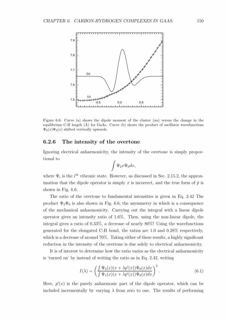
CHAPTER 6. CARBON-HYDROGEN COMPLEXES IN GAAS. 150
-0.5 0.0 0.57.5
7.6
7.7
7.8
7.9
(a)
(b)
Figure 6.6: Curve (a) shows the dipole moment of the cluster (au) versus the change in theequilibrium C-H length (A) for GaAs. Curve (b) shows the product of oscillator wavefunctionsΨ0(x)Ψ2(x) shifted vertically upwards.
6.2.6 The intensity of the overtone
Ignoring electrical anharmonicity, the intensity of the overtone is simply propor-
tional to ∫Ψ2xΨ0dx,
where Ψi is the ith vibronic state. However, as discussed in Sec. 2.15.2, the approx-
imation that the dipole operator is simply x is incorrect, and the true form of p is
shown in Fig. 6.6.
The ratio of the overtone to fundamental intensities is given in Eq. 2.42 The
product Ψ2Ψ0 is also shown in Fig. 6.6, the asymmetry in which is a consequence
of the mechanical anharmonicity. Carrying out the integral with a linear dipole
operator gives an intensity ratio of 1.6%. Then, using the non-linear dipole, the
integral gives a ratio of 0.33%, a decrease of nearly 80%! Using the wavefunctions
generated for the elongated C-H bond, the ratios are 1.0 and 0.28% respectively,
which is a decrease of around 70%. Taking either of these results, a highly significant
reduction in the intensity of the overtone is due solely to electrical anharmonicity.
It is of interest to determine how the ratio varies as the electrical anharmonicity
is ‘turned on’ by instead of writing the ratio as in Eq. 2.42, writing
I(λ) =
(∫Ψ2(x)(x+ λp′(x))Ψ0(x)dx∫Ψ1(x)(x+ λp′(x))Ψ0(x)dx
)2
. (6.1)
Here, p′(x) is the purely anharmonic part of the dipole operator, which can be
included incrementally by varying λ from zero to one. The results of performing

CHAPTER 6. CARBON-HYDROGEN COMPLEXES IN GAAS. 151
0.25
0.50
0.75
0.25 0.50 0.75
(a) (b)
Figure 6.7: The intensity of the overtone versus the degree of electrical anharmonicity λ. TheC-H length is 1.126 A in curve (a) and 1.161 A in curve (b).
this calculation are summarised in Fig. 6.7, which plots the intensity ratio as a
proportion of the value where electrical anharmonicity is absent. It is interesting
to note that for a certain value of λ the intensity ratio is predicted to be zero.
6.2.7 Conclusions
A number of general conclusions can be drawn from this work. They are:
• The bonding parameter, χ, in the effective oscillator mass (Eq. 2.39) need not
be greater than unity to be physical.
• The local density functional approach adopted here can give quantitative in-
formation on the anharmonicity of vibrations.
• Low order perturbation theory cannot be used to describe anharmonic vibra-
tions.
• The intensity of the overtone can be significantly reduced by electrical anhar-
monic effects. In the case of CAs-H in GaAs this may be more than a 70%
reduction.
Specifically concerning the CAs-H in GaAs, it is concluded that the high fre-
quency stretch mode (observed experimentally at 2635 cm−1) is very anharmonic,
some 50% more so than the similar mode in the HCN molecule, and much greater
than the vibration of H on the 〈111〉 surface of diamond where A=113 cm−1 [53].
The reduction in the intensity ratio due to the electrical anharmonicity makes
it tempting to assign the lack of observation of the overtone to a combination

CHAPTER 6. CARBON-HYDROGEN COMPLEXES IN GAAS. 152
of mechanical and electrically anharmonic effects. However, one should bear in
mind that the reorientation barrier for the H to an adjacent bond-centre is only
0.5 eV (Ref. [67]), and the frequency of the overtone is calculated to lie at around
5114 cm−1, which corresponds to an energy of more than 0.6 eV. Thus the lifetime
of the overtone may be too short to allow it to be observed.
6.3 Theory of hydrogenated CAs-dimers.
Recent papers [205, 208] have reported bands of localised vibrational modes (LVMs)
at 2643, 2651, and 2688 cm−1, all of which have been assigned to C-H stretch modes.
It is speculated that the lower two bands are due to CAsH pairs perturbed by the
proximity of another defect, such as a vacancy, an anti-site, or a nearby C-centre.
Interestingly, the 2651 and 2688 cm−1 bands are strongly polarised along one of the
〈110〉 directions perpendicular to the [001] growth direction [216, 217, 218]. This
means that the CAs−H unit is preferentially oriented along a specific 〈110〉 direction.
The [110] and [110] directions are crystallographically equivalent in the zinc-blende
structure, but this is not true at the surface [219]. Using a simple model, Cheng
et al. [216] were able to account the intensities of the 2688 cm−1 band in terms of
the expected concentration of a (CAs-H)-C−As complex. Hence, the model for the
2688 cm−1 band is a pair of substitutional C atoms at neighbouring As sites, with a
single H passivating one of the C acceptors, as indicated schematically in Fig. 6.8.
A series of experiments by Cheng et al. [216] suggest that (CAs)2H dissociates at
around 600C, releasing first a H atom, followed by the dissociation of the C-pairs.
The complex starts to reform by annealing in a H2 ambient at 500C, but would
not be oriented along any particular (110) axis. This suggests that CAs-H defects
are sufficiently mobile at 500C to bond with C-acceptors.
When samples containing the 2688 cm−1 band are exposed to a hydrogen plasma
at 320C, the intensity of the band decreases essentially to zero, and two new
bands at 2725 and 2775 cm−1 bands appear [217]. A subsequent anneal at 450C
removes the 2725 and 2775 cm−1 bands and the polarised 2688 cm−1 band reappears.
Hence, it was thought that these new bands may be due to a (CAs)2H2 complex
which partially dissociates by releasing a single H at 450C whilst the C atoms are
undisturbed. The 2725 and 2775 cm−1 bands do not exhibit the strong polarisation
seen in the 2688 cm−1 band. Further work, however, has suggested that the 2725
and 2775 cm−1 bands do not arise from the same centre [220].
A recent study [221] reported another band at 2729 cm−1 that is polarised. This
band is observed in samples where the 2688 cm−1 band is present, but is polarised
in the orthogonal 〈110〉 direction. It may be that this 2729 cm−1 band comes

CHAPTER 6. CARBON-HYDROGEN COMPLEXES IN GAAS. 153
[-110]
H
[001]CC
Ga As
Figure 6.8: Schematic diagram of the C2H defect thought to be responsible for the 2688 cm−1
band as suggested in Ref.[216].
from a different, metastable (CAs)2H defect in which the CAs-H bond direction is
orthogonal to that in the 2688 cm−1 centre. If this were the case, one would expect
the 2729 cm−1 band to decay under annealing together with a corresponding growth
in the 2688 cm−1 band.
Previous studies [45, 209] have modelled the CGa and the CAs-CGa dimer. Re-
cently, first principles calculations [222] have shown that the model proposed in
Ref. [216] is the lowest energy configuration of the (CAs)2-H complex, and reported
the structures of (CAs)2-H2 complexes, but did not report the local vibrational
modes of these systems. Other models for C-dimers in GaAs have been examined
in literature [223, 224], but these complexes offer no obvious way to explain the
polarisation.
There are three possible configurations for (CAs)2H in which H occupies a bond-
centre located next to C, as indicated in Fig. 6.9. Similarly there are seven possible
configurations of (CAs)2H2, assuming that one H bonds to each C, as indicated in
Fig. 6.10. It is the aim of this paper to establish which sites are most stable, and
to investigate theoretically the assignment made for the 2688 cm−1, and comment
on the 2729, 2725, and 2775 cm−1 vibrational systems.

CHAPTER 6. CARBON-HYDROGEN COMPLEXES IN GAAS. 154
[-110]
[001]C
Ga As
C
12
3
21
Figure 6.9: Schematic diagram of the three configurations of the C2H defect. 1, 2, and 3 labelbond centred sites in which the H atoms have been sited in this study.
15
6[-110]
2 4
7[001]
3
CC
Ga As
21
Figure 6.10: Schematic diagram of seven configurations of the C2H2 defects examined in thispaper. The H sites are labelled using the numbers 1-7, and they can be paired into seven uniquedefect configurations as follows: (1,2), (1,3), (1,4), (3,5), (3,6), (4,5), and (6,7).

CHAPTER 6. CARBON-HYDROGEN COMPLEXES IN GAAS. 155
Atom Wavefunction Charge densityGa 4 × sp 5As 4 × sp 5C 4 × sp 4H 2 × sp 3
Bond-centres 1 × sp 1
Table 6.11: The atomic basis used for the calculations in Sec. 6.3.
6.3.1 Clusters and basis.
In this study, the clusters are centred on a central Ga site surrounded by alternate
shells of As and Ga atoms. Most calculations are based on the defect free cluster
which contains 131 atoms: Ga31As40H60. To model the defects, one or two of the
nearest neighbours to the central Ga are replaced by C, and zero, one, or two H
are placed in the appropriate C-Ga bond centres. The clusters are charged to take
account of the difference in the number of Ga and As atoms. In a number of cases,
a larger, 163-atom cluster (Ga43As44H76) has also been optimised for comparison.
The number of basis functions for Ga, As, C and H are listed in Table 6.11.
The central three shells of atoms are treated in big basis (as defined in Sec. 2.18),
including the central defect atoms. The remaining atoms are in minimal basis,
and a single set of functions was placed between neighbouring atoms. Recalling
the differences between the results with the different bases in the early calculations
of CAs-H, one might consider that this basis is rather small. However, since the
clusters themselves are somewhat larger, the overall cluster basis is reasonable.
6.3.2 Results.
The carbon-dimer is made up of two CAs centres separated by a single Ga site. Since
isolated CAs is a single acceptor, the dimer is expected to be a double acceptor and
the results presented here are for the double negative charge state. Starting with
the two C ionised atoms at neighbouring ideal As lattice sites, all but the surface H
atoms in the 131-atom cluster were relaxed subject to a C2v symmetry constraint.
In the final structure, the C-atoms have moved apart due to the strong Coulomb
repulsion. The final bond-lengths are summarised in Table 6.12. The total energy
of the (C−As)2 system as described above, is around 1.2 eV higher in energy than a
configuration where the two C atoms are separated by two Ga sites, i.e. the (C-Ga-
C)−− structure is metastable. This is consistent with the observations (Ref. [216])
that once H is lost from the defect, it rapidly dissociates.
CHAPTER 6. CARBON-HYDROGEN COMPLEXES IN GAAS. 156
Defect # atoms C1-Ga C1-H C2-Ga C2-H C1-Gaback C2-Gaback
(CAs)2 131 2.18 - 2.18 - 2.02, 2.02, 2.07 2.02, 2.02, 2.07(CAs)-H 132 3.32 1.124 - - 2.03, 2.03, 2.03 -
164 3.27 1.125 - - 1.96, 1.96, 1.96 -(CAs)2-H 132 3.40 1.128 1.94 - 2.01, 2.03, 2.03 2.07, 2.08, 2.08
164 3.36 1.128 1.88 - 1.95, 1.96, 1.96 1.99, 2.00, 2.03(CAs)2-H2 133 3.44 1.127 1.94 1.120 2.01, 2.02, 2.04 2.02, 2.02, 3.52
165 3.41 1.129 1.89 1.132 1.94, 1.96, 1.97 1.97, 1.97, 3.35
Table 6.12: The bond lengths of the relaxed (CAs)2, (CAs)−H, (CAs)2 −H and (CAs)2 −H2. TheC1-Ga and C2-Ga lengths are to the common Ga neighbour. The ‘back’ bonds refer to the threeremaining C-Ga separations shown in Figs. 6.9 and 6.10. All lengths are in A.
6.3.2.1 The (CAs)2-H complex.
Fig. 6.9 shows schematically the three sites that the H can adopt if one assumes
that the H atom lies at a C-Ga bond-centre. In each case, all but the surface
atoms in the 132 atom cluster were relaxed, and we have assumed that the centre
would be a single acceptor. From our calculations, the lowest energy configuration
is that suggested by Cheng et al. with the H in the bond-centre site 1 in Fig. 6.9.
The configurations with the H atoms at sites 2 and 3 are 0.5 and 0.9 eV less stable
respectively. The bond-lengths and LVMs of the lowest energy structure are listed in
Tables 6.12 and 6.13 respectively. The calculated C-H stretch mode is 2826 cm−1,
5% greater than the experimental value of 2688 cm−1, which is within the error
bounds of the method. The lower lying modes are characterised by C-H wag and
C-related modes.
Defect masses 132 atoms 164 atoms12C1-H-Ga-12C2 2826 283012C1-D-Ga-12C2 2070 207213C1-H-Ga-12C2 2818 282213C1-D-Ga-12C2 2059 2061
Table 6.13: The C-H stretch modes of the lowest energy C1-H-Ga-C2 system (cm−1) for thevarious combinations of carbon and hydrogen isotopes in the 132 and 164 atom clusters. Note,the C1-H stretch mode is unaffected by a change in mass of C2.
It is pertinent to compare these results with the structure and modes of the CAsH
centre. The final CAs-H bond length was 1.12 A, which is very slightly (∼ 0.3%)
shorter than that of C2H. Generally, the shorter the C-H bond-length, the higher one
would expect the LVM to be, however, the calculated C-H stretch mode of the CAsH
centre was also 2826 cm−1. Thus, the experimentally observed 53 cm−1 splitting
between the 2635 and 2688 cm−1 bands is not reproduced in these calculations.
Previous studies have shown that anharmonic terms are important for C-H stretch

CHAPTER 6. CARBON-HYDROGEN COMPLEXES IN GAAS. 157
modes in GaAs [40]. In general, the anharmonic corrections for the two defects
would be different, and this might account for the discrepancy. Perhaps more
fundamentally, however, LVMs are extremely sensitive to the C-H length: roughly,
a 3% change in bond length gives rise to a 10% change in the LVM. Applying this
to the C2H complex, a decrease in bond length of around 0.01 A would increase the
stretch mode to lie 50 cm−1 above that of CAsH. To test this hypothesis, the C-H
bond in the (CAs)2H system was shortened to 1.12 au (a decrease of 1%), and the
LVMs re-evaluated. The stretch mode increased to 2913 cm−1 (an increase of 3%).
The total energy of the system increased by around 2 meV. Thus, the calculated
frequencies are consistent with experiment to within the limitations of the method.
Now, for the stretch mode to be polarised along [110], it is sufficient to show
that the displacement of the H atom is also along [110]. Our calculation shows this
to be the case, and we list the projection of the normal co-ordinates onto the [110],
[110] and [001] directions in Table 6.14. In fact, this is also the case with the H
[110] [110] [001]C1 0.00 0.21 -0.17C2 0.00 0.00 0.00H 0.00 -0.75 0.61
Table 6.14: The projection onto the [110], [110], and [001] directions of the C-H stretch mode ofthe C1h symmetry (CAs)2H complex, calculated in the 132 atom cluster (cm−1). The C atoms arelabelled 1 and 2 according to Fig. 6.9. The mode is symmetric about the C1h mirror plane.
atom in either of the other bond-centred sites. The only requirement for the C-H
stretch mode to be polarised is that the C-dimers must be preferentially aligned in
one 〈110〉 direction.
The stability of the defect can be seen from the following argument. When H
is at site 1 (Fig. 6.9), the Ga neighbour with the broken bond relaxes away from
the C-H unit and becomes close to C2, relieving the local strain. Now, a larger
C-(H)-Ga separation tends to lead to a shorter C-H bond due to a reduction in
the covalent bonding with the Ga atom. If H is at site 3, the Ga neighbour does
not relax to the same extent since there is no local strain there. This leads to a
relatively long C-H bond and hence a lower vibrational frequency. The C-H stretch
mode for the high energy C2H configuration with H at site 3 is calculated to lie at
2774 cm−1. Consistent with the above argument, this is somewhat lower than that
of the lowest energy structure (site 1). Consequently, this metastable defect cannot
account for the experimentally observed 2729 cm−1 band polarised orthogonally to
the 2688 cm−1 band.

CHAPTER 6. CARBON-HYDROGEN COMPLEXES IN GAAS. 158
Model (1,2) (1,3) (1,4) (3,5) (3,6) (4,5) (6,7)Stretch modes 2640 2895 2819 2791 2749 2806 2783
2586 2836 2779 2770 2747 2803 2779Etot 133 atoms 0.95 0.00 0.26 0.22 0.75 0.03 0.64
165 atoms - 0.00 - - - 0.16 -
Table 6.15: The C-H stretch modes for the 133 atom clusters (cm−1) and total energies for the 133and 165 atom clusters, Etot (eV), relative to the (1,3) pairing for the seven configurations of the(CAs)2H2 complex. The models are labelled according to pairing of hydrogen atoms as describedin Fig. 6.10.
Isotopes 133 atoms 165 atoms12C1-H-Ga-12C2-H 2836, 2895 2827, 278813C1-H-Ga-12C2-H 2829, 2895 2819, 278812C1-D-Ga-12C2-H 2077, 2895 2069, 278813C1-D-Ga-12C2-H 2066, 2895 2058, 278812C1-H-Ga-13C2-H 2836, 2887 2826, 278012C1-H-Ga-12C2-D 2836, 2121 2826, 203912C1-H-Ga-13C2-D 2836, 2109 2826, 2029
Table 6.16: The C-H stretch modes of the lowest energy (CAs)2H2 model (1,3) (Fig. 6.10) in the133 and 165 atom clusters (cm−1). Since the two C-H units are practically decoupled, only asubset of the permutations of isotopes is required. The modes are not shifted significantly by theGa mass.
6.3.2.2 The (CAs)2-H2 complex.
There are a number of possible configurations of the defect. If one assumes that
both of the H atoms are approximately C-Ga bond centred, and only one H atom
is bonded to each of the C atoms, then there are seven possible combinations of
sites. The possible H locations are shown schematically in Fig. 6.10, labelled 1-7,
and the seven combinations are denoted by the sites of the pairs of H atoms: (1,2),
(1,3), (1,4), (3,5), (3,6), (4,5), and (6,7). All of these defects are fully passivated,
and the band-gap is free from defect levels.
The lowest energy system is (1,3), and the total energy of each model quoted
in Table 6.15 relative to this. The two C-H and stretch modes are also listed in for
each configuration. Note, the (1,3) pairing is only marginally more stable than that
of (4,5). This result may be sensitive to cluster size, and we investigate below the
results in larger clusters.
The various bond lengths of the (1,3) model are listed in Table 6.12, and the
values of the stretch modes for the H and C isotopes are listed in Table 6.16. It
can be clearly seen the two H atoms are practically decoupled. As with (CAs)2H,
the normal modes of the (CAs)2H2 are polarised in the [110] and [110] directions,

CHAPTER 6. CARBON-HYDROGEN COMPLEXES IN GAAS. 159
133 atoms 165 atomsMode [110] [110] [001] Mode [110] [110] [001]
C1 2895 0.00 0.01 -0.01 2827 0.00 -0.21 0.16H1 0.00 -0.03 0.02 0.01 0.76 -0.58C2 0.23 0.01 0.14 -0.02 0.00 -0.01H2 -0.81 -0.04 -0.51 0.08 -0.01 0.04C1 2836 -0.01 -0.21 0.16 2788 0.00 -0.02 0.02H1 0.02 0.76 -0.59 0.00 0.07 -0.05C2 0.01 0.00 0.01 0.23 -0.03 0.12H2 -0.03 0.00 -0.02 -0.84 0.12 -0.45
Table 6.17: The projection onto the [110], [110], and [001] directions of the normal stretch modesof the C1 symmetry (CAs)2H2 complex (cm−1). The C atoms are labelled 1 and 2 according toFig. 6.10.
and consequentially the IR absorption of the system should be strongly polarised.
In fact, all of the seven models examined for this centre would also be strongly
polarised, and it is unlikely that there is a configuration that would not be po-
larised since in each case the C-H bond directions are largely in the [110] and [110]
directions. The normal coordinates of each of the stretch modes projected onto
the [110], [110], and [001] directions are listed in Table 6.17. These show that the
deviation from [110] and [110] polarisation of the vibrations due to the relaxation
of the atoms is to small to account for the lack of polarisation observed in the 2725
and 2775 cm−1 bands. Therefore, since the experimental bands are not polarised,
they cannot be attributed to the (CAs)2H2 complex.
As stated above, the calculated values of the LVMs are extremely sensitive to
bond lengths, which are in turn affected by the proximity of the centre to the
cluster surface. To explore the effect of cluster size in the case of the lowest energy
configuration we have also calculated the relaxed structure and LVMs for the (1,3)
and (4,5) systems for the (CAs)2H2 complex in the 165 cluster. Then the (1,3)
system is again more stable than the (4,5) pairing by 0.16 eV. The final (1,3) pair
structure possessed C-H bond lengths of 1.129 and 1.132 A, and stretch modes
lying at 2827 cm−1 and 2787 cm−1 for the stretches involving the hydrogen atoms
at sites 1 and 3 respectively in Fig. 6.10. However, in contrast with the calculation
performed on the smaller cluster, the lower frequency mode now arises from the H
atom at site 3. The calculated splitting of the two stretch modes is 40 cm−1. A
summary of the bond lengths and local modes are listed in Tables 6.12 and 6.16
respectively.
As with the smaller cluster, the modes are polarised in the [110] and [110]
directions (Table 6.17). For comparison, we have also calculated the structures and
LVMs of the CAsH and (CAs)2H systems in 164 atom clusters, and they possess
CHAPTER 6. CARBON-HYDROGEN COMPLEXES IN GAAS. 160
stretch modes of 2820 and 2830 cm−1 respectively. The bond lengths are listed in
Table 6.12.
As indicated above, the (CAs)2H2 complex has two stretch modes polarised in
orthogonal directions. It may be that the 2729 cm−1 band, which cannot be assigned
to (CAs)2H, is due to one of these modes. However, this leaves a second band (higher
in frequency) undetected, which should be polarised in the same direction as the
2688 cm−1 band.
6.3.3 Conclusions.
The lowest energy structure of (CAs)2H is planar in agreement with the model
put forward by Cheng et al. [216] shown in Fig. 6.8 and also with recent calcula-
tions. [222] The (CAs)2H2 complex is not planar and the H atoms lie in the bond
centred sites marked 1 and 3 in Fig. 6.10. This is also in agreement with recent
calculations [222]. The LVMs calculated for these systems broadly agree with the
assignments of the (CAs)2H complex to the 2688 cm−1. It is possible that the
2729 cm−1 band observed by Stavola et al. arises from the [110] polarised mode
of this system, but no second mode was detected. These calculations do not sup-
port the hypothesis that a metastable (CAs)2H configuration is responsible for the
2729 cm−1 band.

Chapter 7
Conclusions
A conclusion is the place where you got tired of thinking.
- Arthur Block
Although detailed conclusions have been presented at the appropriate places in
Chapters 4 to 6, it is worth making a few more general conclusions about the way
in which AIMPRO has been used to examine the various defects. Suggestions are
made for where areas presented here might be extended.
The detailed study of a number of vacancy-impurity complexes in diamond
has revealed that the techniques used here are able to describe semi-quantitatively
transition energies and radiative lifetimes. More significantly, in all the situations
explored, the symmetries of the ground and excited states have been found to agree
with experiment. In the case of the complex of Si with a vacancy, the code was able
to predict the unusual structure. Without such a structure it is difficult to imagine
how such a centre could give rise to the experimental observations.
The attempts thus far in producing n-type diamond by doping with phosphorus
have been mainly unsuccessful. The calculations on the phosphorus-vacancy com-
plex may go some way to explaining why this is. There have been suggestions that
alternative ways of generating shallow levels might be analogous to the so called
‘shallow thermal donors’ seen in silicon. These are thought to be formed when deep
donor centres are forced up in energy by the proximity of neighbouring oxygen
atoms [225]. Calculations are under way to see how similar complexes in diamond
behave.
Ni in diamond has been of interest for more than a decade as catalytic synthesis
has become more important. The work presented here has two main implications:
first, Ni and Ni-X complexes possess a large number of optical transition mechanisms
but in each case there is expected to be a single rate dominant transition. Secondly,
the previous assignments of interstitial Ni to optically and electrically active centres
161

CHAPTER 7. CONCLUSIONS 162
is found wanting. We find that there is no requirement for Nii and the previous
assignments involving this centre may be incorrect.
There are a large number of further Ni and Co related complexes that require
study, most importantly the apparent aggregation of N at these impurities under
annealing. This work has been started. Another centre that is thought to be crucial
to the understanding of at least Ni in diamond is the Ni-vacancy complex, which is
thought to be the core at the centre of the class of EPR centres labelled NE1-7. A
number of attempts have been made using AIMPRO to establish the ground state
structure and electronic properties. However, to date there have been significant
difficulties in establishing self-consistency. This is, at least in part due to the rather
large number of fitting functions required to model the charge density, which in
turn leads, in this case, to instability in the calculation.
There remain a number of other problems of great interest that are difficult to
treat using the approach adopted for this thesis. Of these, the most significant might
be why Ni related centres are exclusively found in the octahedral growth sectors.
In fact, this is true of other centres, including Co. This polarisation is thought
to arise during growth, but simulating this has proved difficult, since it requires
the calculation of the relative stabilities of impurity atoms on different surfaces.
Another question is why only Ni and Co are found as dispersed impurities, despite
the fact that the whole range of first row transition metals are used in diamond
synthesis.
Finally, it is worth noting that a number of Ni-related centres exhibit structure
due to spin-orbit interaction; in principle, this effect can be treated using AIMPRO,
since the Bachelet, Hamann, and Schluter [11] pseudopotential contain spin-orbit
parameters. Naturally, including spin-orbit effects would cost significant extra com-
puting time.
Often, subtle effects (such as Jahn-Teller distortions) are seen experimentally,
and it is desirable to be able to resolve these computationally. Two examples
contained in this thesis are as follows. For Ni−s in Si, it has been shown that
the ground state ordering of one-electron levels can be established for the Jahn-
Teller distorted system. This is achieved by adopting a sophisticated algorithm that
dictates which Kohn-Sham eigenvalues are occupied throughout the self-consistent
cycle, and thus avoids discontinuous changes in charge density (so called charge
sloshing). In fact a similar approach must be adopted to determine the energies of
multiplets as in the [V-N]− complex in diamond.
In contrast to these successes, the sensitivity of the vibrational modes of CAs-
H centres in GaAs to the C-H bond-lengths has proved difficult to resolve. This

CHAPTER 7. CONCLUSIONS 163
regrettably leads to a degree of empiricism to justify certain interpretation1. How-
ever, since this arises from the density functional theory at the very root of the
calculations, there is no obvious route to a better method.
However, when combined with total energies, vibrational modes can be a highly
discriminative tool. As an illustration, one can turn to Ni-H2 in Si. Here, the
location of H with respect to the Ni atom, that is whether the H is bond-centred
or anti-bonded, is hard to discriminate purely on the grounds of total energies.
In fact most arrangements are of a similar energy, but the crucial difference is in
the vibrational modes. This will most likely prove to be important in the case of
gold-hydrogen complexes which are also under investigation.
As highlighted above, a number of difficulties can be traced to either the fact that
the calculations are performed in clusters or there is a problem with the intermediate
fit to the charge density. To a large extent, these are solved in a new incarnation
of AIMPRO, where the calculations are performed using super-cells, and hence the
intermediate fit to the charge density is no longer required. This eliminates the
near instability in some situations involving atoms whose basis includes d-orbitals,
such as Ni-V. Furthermore, calculations of more ionic III-V compounds (such as
GaN) as well as the interesting II-VI compounds will also become possible, since
the super-cell would not suffer from problem of charge building up at surfaces in
the case of clusters.
Whether it is the cluster or super-cell approach, the parallelisation of AIMPRO
has lead to two important improvements. First, a 71-atom cluster made up from
atoms with s- and p-orbitals can be relaxed very quickly, and single energies cal-
culated in minutes rather than hours. Secondly, very large clusters can be used,
without which the study of extended defects (such as the (CAs)2-H2 centres in GaAs)
would be difficult. Furthermore, a new area of interest being developed in the AIM-
PRO group is that of proteins and related biological molecules. Even the smallest
of these systems contain several hundreds of atoms, and without massively parallel
computer platforms, relaxation would be prohibitively slow.
However, there is a severe problem in obtaining relaxed structures for such
highly complex molecules, and this is the number of local energy minima. In fact,
one can break down a molecule such as a peptide into smaller units - in this case
amino acids. Each of these groups will have a number of local minima. Therefore,
it is likely that a new strategy will be adopted for the minimisation of the energy,
perhaps by calculating the forces using some form of parameterisation of the force
constants, hydrogen bonding and so on.
1This refers to the 10% change in vibrational frequency for a 3% change in bond-length.

CHAPTER 7. CONCLUSIONS 164
In conclusion, theory can be viewed from two points: first, it can be an aid to
experiment, where it is used to explain observation. The second is perhaps more
significant, in that theory can be used as a predictive tool, guiding further experi-
ments. For example, the predictions that [Si-V] and [Si-V]− would be paramagnetic,
and current experiments are underway to test this hypothesis.

Appendix A
Character tables
Tabulated here are character tables for the 3 point groups most often discussed
in this thesis: in the Schoenflies (international) notation, C2v (2mm), C3v (3m)
and Td (43m). (For a detailed explanation of their derivation and use, see for
example Ref. [226], from which these tables are taken.) Each table also shows
some combinations of the coordinates (x, y, z) that transform according to each
irreducible representation (IR).
Each IR is denoted by A or B if it is one dimensional, and E or T if it is 2-
or 3-dimensional, respectively. The dimensionality is linked to the degeneracies
of one-electron Kohn-Sham levels (except for the case of accidental degeneracy),
which are usually labelled in lower case. Thus, for example, a Kohn-Sham level
that transforms as t2 in the Td point group is three-fold degenerate (as well as spin
degenerate). Such a level can therefore be occupied by up to 6 electrons.
The symmetry operations are as follows: e is the identity operation; Cn is a
rotation through 2π/n; σv is a reflection in a vertical plane (passing through the
symmetry axis); σd is a reflection in a diagonal plane; and Sn is an improper rotation
of 2π/n. In the case of C2v there are two inequivalent σv operations, one of which
is identified by a prime.
C2v e C2 σv σ′v
A1 1 1 1 1 x2; y2; z2; zA2 1 1 -1 -1 xyB1 1 -1 1 -1 xz; xB2 1 -1 -1 1 yz; y
C3v e 2C3 3σv
A1 1 1 1 x2 + y2; z2; zA2 1 1 -1E 2 -1 0 (x2 − y2, xy);
(x, y); (xz, yz)
Td e 8C3 2C2 6σd 6S4
A1 1 1 1 1 1A2 1 1 1 -1 -1E 2 -1 2 0 0T1 3 0 -1 -1 1T2 3 0 -1 1 -1 (x, y, z)
165

Appendix B
Jahn-Teller distortions
The Jahn-Teller theorem applied to the (ground-state) one-electron picture of the
Kohn-Sham levels can be understood as follows (in the absence of spin-orbit inter-
action).1 If the highest occupied one-electron level is degenerate and partially occu-
pied, then the system may distort to a lower symmetry such that the degeneracy is
lifted. This will lower the total energy provided the reduction in the energy of the
occupied orbital(s) is greater than any increase in energy due to the distortion. This
follows from the fact that the total energy is related to the sum of the one-electron
energies.
Take as an example, a t2 level in tetrahedral symmetry containing two electron.
This is the case for the neutral vacancy in silicon. A trigonal distortion will split the
t2 level into an singlet (a1) and a doublet (e). This is illustrated in Fig. B.1(a)→(b).
The addition of a further electron makes the e-level unstable, and a further Jahn-
Teller distortion (say C2v) will split this doublet into two singlets – b1 and b2 – as
shown in Fig. B.1(b)→(c).
t2a1 a1
b2
b1
Td C2vC3v
e
(a) (b) (c)
Figure B.1: A diagram showing the splittings of a t2-level with C3v and C2v distortions to illustratethe Jahn-Teller effect.
1Only the static Jahn-Teller effect is discussed. For a more detailed explanation of the Jahn-Teller effect, see Ref. [104], and references therein.
166
APPENDIX B. JAHN-TELLER DISTORTIONS 167
If the trigonal distortion had resulted in the e-level below the a1, this would
also be unstable against a Jahn-Teller distortion, provided that Hund’s rule is not
obeyed, i.e. the electrons have opposite spins. If instead the electrons are aligned,
i.e. a spin S=1 centre, then no Jahn-Teller distortion would be expected.
The above principles can naturally be applied to excited states. Thus, a excited
state generated by promoting an electron from the a1 to e level in Fig. B.1(b) would
be a candidate for a further Jahn-Teller distortion.

Bibliography
[1] P. N. Keating, Phys. Rev. 145, 637 (1966).
[2] J. Tersoff, Phys. Rev. B 56, 632 (1986).
[3] A review of Hartee-Fock theory and its derivation can be found in ‘Many-Body
Theory of Solids’ by J. C. Inkson, (Plenum Press, New York, 1984).
[4] P. Hohenberg, and W. Kohn, Phys. Rev. B 136 864 (1964).
[5] W. Kohn, and L. J. Sham, Phys. Rev. A 140, 1133 (1965).
[6] J. E. Northrup and S. Froyen, Phys. Rev. B 50, 2015 (1994).
[7] G. P. Srivastava and S. J. Jenkins, Phys. Rev. B 53, 12589 (1996).
[8] P. K. Sitch, PhD Thesis, ‘Ab-initio calculations of dislocation related properties
in semiconductors’ 1994; P. Sitch, R. Jones, S. Oberg, and M. I. Heggie, Phys.
Rev. B 50, 17717 (1994); S. Oberg, P. K. Sitch, R. Jones, and M. I. Heggie,
Phys. Rev. B 51, 13138 (1995); P. Sitch, R. Jones, S. Oberg, and M. I. Heggie,
Phys. Rev. B 52, 4951 (1995).
[9] See for example: R. Jones. C. D. Latham, M. I. Heggie, V. J. B. Torres, S.
Oberg, and S. K. Estreicher, Phil. Mag. Lett. 65, 291 (1992); S. K. Estreicher,
C. D. Latham, M. I. Heggie, R. Jones, and S. Oberg, Chem. Phys. Lett. 196,
311 (1992).
[10] A. Resende, R. Jones, S. Oberg, P. R. Briddon, and B. R. Eggen, unpublished
report (1996).
[11] G. B. Bachelet, D. R. Hamann, and M. Schluter, Phys. Rev. B 26, 4199 (1982).
[12] A. N. Safonov, E. C. Lightowlers, G. Davies, P. Leary, R. Jones, and S. Oberg,
Phys. Rev. Lett. 77, 4812 (1996).
[13] B. Bech Neilsen, L. Hoffmann, M. Budde, R. Jones, J. Goss, and S. Oberg,
Mat. Sci. Forum 196-201, Trans Tech Publications, Switzerland, p. 825-829
(1995).
168

BIBLIOGRAPHY 169
[14] To appear in Identification of Defects in Semiconductors, ed. M. Stavola, Semi-
conductors and Semimetals, treatise editors, R. K. Willardson, A. C. Beer, and
E. R. Weber, Academic Press.
[15] A. M. Stoneham, Defects in Solids, Oxford University Press, London (1975).
[16] J. C. Slater, Quantum Theory of Atomic Structure, Vol. 2, McGraw Hill, New
York (1960).
[17] See for example J. A. Pople, and D. L. Beverage, ‘Approximate Molecular
Orbital Theory’ McGraw-Hill, New York (1970).
[18] R. G. Parr, J. Chem. Phys. 20, 239 (1952).
[19] J. A. Pople, D. P. Santry, and G. A. Segal, J. Chem. Phys. 43, S129 (1965).
[20] M. Goeppert-Mayer, and A. L. Sklar, J. Chem. Phys. 6, 645 (1938).
[21] J. A. Pople, D. L. Beverage, and P. A. Dobosh, J. Chem. Phys. 47, 158 (1967)
[22] R. N. Dixon, Mol. Phys. 12, 83 (1967).
[23] J. C. Slater, Quantum Theory of Atomic Structure, Vol. 1, McGraw Hill, New
York (1960).
[24] L. Paslovsky, and J. E. Lowther, J. Phys. Chem. Solids 54, 243 (1993).
[25] J. Isoya, H. Kanda, J. R. Norris, J. Tang, and M. K. Bowman, Phys. Rev. B
41, 3905 (1990).
[26] D. M. Ceperley, and B. J. Alder, Phys. Rev. Lett. 45, 566 (1980).
[27] J. P. Perdew, and A. Zunger, Phys. Rev. B 23, 5048 (1981).
[28] U. von Barth, and L. Hedin, J. Phys. C 5, 1629 (1972).
[29] See for example J. P. Perdew, J. A. Chevary, S. H. Vosko, K. A. Jackson, M.
R. Pederson, D. J. Singh, and C. Fiolhais, Phys. Rev. B 46, 6671 (1992).
[30] L. Hedin Phys. Rev. 139, A796 (1965).
[31] R. Delsole, L. Reining, R. W. Godby, Phys. Rev. B 49, 8024 (1994).
[32] D. Vanderbilt, Phys. Rev. B 41, 7892 (1990)
[33] S. G. Louie, S. Froyen, and M. L. Cohen, Phys. Rev. B 26, 1738 (1982).

BIBLIOGRAPHY 170
[34] X. J. Chen, J. M. Langlois, and W. A. Goddard, Phys. Rev. B 52, 2348 (1995).
[35] B. I. Dunlap, W. J. Connolly, and J. R. Sabin, J. Chem. Phys. 71, 4993 (1979).
[36] R. Jones, and A. Sayyash, J. Phys. C: Solid State Phys. 19, L653 (1986).
[37] G. M. S. Lister, and R. Jones, unpublished (1988).
[38] H. Hellmann, Einfuhrung in die Quantenchemie (Deuticke, Leipzig 1937); R.
P. Feynman Phys. Rev. 56 340 (1939).
[39] M. Born, and K. Huang, Dynamical Theory of Crystal Lattices, Oxford Uni-
versity Press, London (1954).
[40] R. Jones, J. Goss, C. P. Ewels, S. Oberg, Phys. Rev. B 50, 8378 (1994).
[41] M. J. P. Musgrave, J. A. Pople, Proc. Roy. Soc. A268, 474 (1962).
[42] R. Jones, J. Phys. C: Solid St. Phys. 21, 5735 (1988).
[43] R. Jones, J. Phys. C: Solid St. Phys. 20, 271 (1987).
[44] F. Berg Rasmussen, R. Jones, and S. Oberg, Phys. Rev. B 50, 4378 (1994).
[45] R. Jones, and S. Oberg, Phys. Rev. B 44, 3673 (1991).
[46] R. Jones, and S. Oberg, Phys. Rev. B 49, 5306 (1994).
[47] C. P. Ewels, S. Oberg, R. Jones, B. Pajot, and P. R. Briddon, Semicond. Sci.
and Technol. 11, 502 (1996).
[48] J. Purton, R. Jones, M. Heggie, S. Oberg, C. R. A. Catlow, Phys. Chem.
Minerals 18, 389 (1992).
[49] R. Jones, P. R. Briddon, and S. Oberg, Phil. Mag. Lett. 66, 67 (1992).
[50] Y. J. Chabal, and C. K. N. Patel, Phys. Rev. Lett. 53, 210 (1984).
[51] B. R. Davidson, R. C. Newman, T. J. Bullough, and T. B. Joyce, Phys. Rev.
B 48, 17106 (1993).
[52] R. C. Newman, Semicond. Sci. and Technol. 5, 911 (1990).
[53] Xuejun Zhu, and S. G. Louie, Phys. Rev. B 45, 3940 (1992).
[54] R. C. Newman, Physica B 170, 409 (1991).
[55] P. M. Morse, Phys. Rev. 34, 57 (1929).

BIBLIOGRAPHY 171
[56] R. Darwich, B. Pajot, B. Rose, D. Robein, B. Theys, R. Rahbi, C. Porte, and
F. Gendron, Phys. Rev. B 48, 17776 (1993).
[57] R. S. Leigh, and B. Szigeti, Proc. Roy. Soc., A 301, 211 (1967).
[58] B. Clerjaud, and D. Cote, J. Phys. Condens. Matter 4, 9919 (1992).
[59] U. von Barth, Phys. Rev. A 20, 1693 (1979).
[60] J. P. Goss, R. Jones, S. J. Breuer, P. R. Briddon, and S. Oberg, Phys. Rev.
Lett. 77, 3041 (1996).
[61] O. Svelto, Principles of Lasers, Plenum Press, New York (1976).
[62] A. J. Dekker, Solid State Physics (MacMillan, London) 1958.
[63] See for example A. S. Barker, A. J. Sievers, Rev. Mod. Phys. 47, 51 (1975); R.
C. Newman, ‘Infrared studies of crystal defects’ (Taylor and Francis, London)
1973; R. C. Newman, ‘Localised vibrational mode spectroscopy’ ed. R. A.
Stradling, and P. C. Klipstein, Adam Hilger, Bristol and New York, 1990.
[64] Landolt-Bornstein New Series Group III Vol. 17 Semiconductors Sub Vol a:
Physics of Group IV Elements and III-V Compounds (Springer-Verlag, Berlin-
Heidelberg, 1982) and references therein
[65] G. A. Gledhill, S. S. Kudhail, R. C. Newman, J. Woodhead, G. Z. Zhang, J.
de Physique, Colloq. C6, Suppl. No. 12, 42, 685 (1981).
[66] J. B. Clegg, ‘Depth profiling of semiconductor materials by secondary ion mass
spectroscopy’ in ‘Growth and characterisation of semiconductors’ ed. R. A.
Stradling, and P. C. Klipstein, Adam Hilger, Bristol and New York, 1990.
[67] B. Clerjaud, D. Cote, F. Gendron, W-S. Hahn, M. Krause, and C. Porte,
Materials Science Forum 83-7, 563 (1991).
[68] G. D. Watkins, Proceedings of the NATO Advanced Research Workshop on
‘Early Stages of Oxygen Precipitation in Silicon’, ed. R. Jones, Kluwer Aca-
demic Press, pp. 1-18 (1996).
[69] P. S. Nandhra, R. C. Newman, R. Murray, B. Pajot, J. Chevalliear, R. B. Beall,
and J. J. Harris, Semicond. Sci. and Tech. 3, 356 (1988).
[70] J. Wagner, K. H. Bachem, B. R. Davidson, R. C. Newman, T. J. Bullough,
and T. B Joyce, Phys. Rev. B 51, 4150 (1995).

BIBLIOGRAPHY 172
[71] W. Low, ‘Paramagnetic resonance in solid state physics: advances in research
and applications’, ed. F. Seitz and D. Turnball, Academic Press, New York,
1960.
[72] G. D. Watkins, ‘Point defects in solids’, ed. J. H. Crawford (Jr.), and L. M.
Slifkin, Vol. 2, Semiconductors and molecular crystals, Plenum, New York,
1975.
[73] X. Zhou, G. D. Watkins, K. M. McNamara Rutledge, R. P. Messmer, and
Sanjay Chawla, Phys. Rev. B 54, 7881 (1996).
[74] M. F. Thomaz, and G. Davies, Proc. Roy. Soc. London A 362, 405 (1978).
[75] D. L. Dexter, ‘Solid State Physics’, Vol. 6, ed. F. Seitz and D. Turnball, Aca-
demic Press, New York, 1958.
[76] A. T. Collins, M. F. Thomaz, and M. I. B. Jorge, J. Phys. C: Solid State Phys.
16, 2177 (1983).
[77] S. Lawson, private communication.
[78] M. Tajima, Appl. Phys. Lett. 32, 719 (1978).
[79] P. McL. Colley, and E. C. Lightowlers, Semicond. Sci. and Technol. 2, 157
(1987).
[80] E. C. Lightowlers, ‘Photoluminescence Characterisation’ in ‘Growth and char-
acterisation of semiconductors’ ed. R. A. Stradling, and P. C. Klipstein, Adam
Hilger, Bristol and New York, 1990.
[81] G. Davies, J. Phys. C: Solid State Phys. 12, 2551 (1979).
[82] See for example D. V. Lang, J. Appl. Phys. 45, 3023 (1974); G. L. Miller, D.
V. Lang, and L. C. Kimerling, Ann. Rev. Mater. Sci. pp 377-448, 1977.
[83] See for example D. W. Palmer ‘Characterisation by capacitance methods’ in
‘Growth and characterisation of semiconductors’ ed. R. A. Stradling, and P.
C. Klipstein, Adam Hilger, Bristol and New York, 1990.
[84] A. Matthews, and S. S. Eskildsen, Diamond and Rel. Mat. 3, 902 (1994).
[85] S. Dannefaer, W. Zhu, T. Bretagnon, and D. Kerr, Phys. Rev. B 53, 1979
(1996).

BIBLIOGRAPHY 173
[86] G. Davies, S. C. Lawson, A. T. Collins, A. Mainwood, S. Sharp, Phys. Rev. B,
46, 13157 (1992).
[87] C. A. Coulson, and M. Kearsley, Proc. Roy. Soc. London Ser. A 241, 433
(1957).
[88] G. Davies, Nature 269, 498 (1977).
[89] J. Isoya, H. Kanda, Y. Uchida, S. C. Lawson, S. Yamasaki, H. Itoh, and Y.
Morita, Phys. Rev. B 45, 1436 (1992).
[90] A. Mainwood, J. Phys. C 11, 2703 (1978).
[91] J. E. Lowther, and J. A. van Wyk, Phys. Rev. B 49, 11010 (1994).
[92] S. J. Breuer, PhD Thesis, ‘A First Principles Study of Defects in Diamond’,
1994.
[93] S. J. Breuer and P. R. Briddon, Phys. Rev. B 51 6984 (1995).
[94] J. E. Lowther, Phys. Rev. B 48, 11594 (1993).
[95] X.-F. He, N. B. Manson, and P. T. H. Fisk, Phys. Rev. B 47, 8816 (1993).
[96] A. Mainwood, Phys. Rev. B 49, 7934 (1994).
[97] G. Davies, and M. F. Hamer, Proc. Roy. Soc. London Ser. A 348, 285 (1976).
[98] X.-F. He, N. B. Manson, and P. T. H. Fisk, Phys. Rev. B 47, 8816 (1993).
[99] Y. Mita, Phys. Rev. B 53, 11360 (1996).
[100] M. E. Newton, private communication (1996).
[101] G. Davies, M. H. Nazare, and M. F. Hamer, Proc. Roy. Soc. London Ser. A
351, 245 (1976)
[102] C. D. Clark, R. W. Ditchburn, and H. B. Dyer, Proc. Roy. Soc. London Ser.
A 234, 363 (1956).
[103] F. S. Ham, Phys. Rev. 166, 307 (1968).
[104] M. Lannoo and J. Bourgoin, Point defects in semiconductors, Vols. I and II,
Springer series in Solid-State Sciences 22 and 35, Ed. M. Cardona, Springer-
Verlag, New York 1981.
[105] P. A. Crowther and P. J. Dean, J. Phys. Chem. Solids 28, 1115 (1967).

BIBLIOGRAPHY 174
[106] G. Davies, in The Properties of Diamond, edited by J. E. Field (Academic
Press, London, 1979), p. 165.
[107] J. van Wyk, J. Phys. C: Solid State Phys. 15, L981 (1982).
[108] G. Davies, C. M. Welbourn, and J. H. N. Loubser, Diamond Research 1978,
published by de Beers Industrial Diamond Division, Ascot, UK, pp. 23-30.
[109] A. M. Zaitsev, V. S. Vavilov, and A. A. Gippius, Sev. Phys. Leb. Inst. Rep.
10, 15 (1981).
[110] J. Ruan, W. J. Choyka, and W. D. Partlow, Appl. Phys. Lett. 58, 295 (1991).
[111] L. H. Robins, L. P. Cook, E. N. Frabaugh, and A. Feldman, Phys. Rev. B 39,
3212 (1989).
[112] A. T. Collins, L. Allers, C. J. H. wort, and G. A. Scarsbrock, Diamond and
Rel. Mat. 3 932 (1994).
[113] C. D. Clark, H. Kanda, I. Kiflawi, and G. Sittas, Phys. Rev. B 51, 16681
(1995).
[114] H. Sternschulte, K. Thonke, R. Sauer, P. C. Munzinger, and P. Michler, Phys.
Rev. B 50, 14554 (1994).
[115] K. Jackson, M. R. Pederson, and J. G. Harrison, Phys. Rev. B 41 12641
(1990).
[116] S. A. Kajihara, A. Antonelli, J. Bernholc, and R. Carr, Phys. Rev. Lett. 66,
2010 (1991).
[117] R. Jones, S. Oberg, Phil. Mag. Letters 64, 317 (1991).
[118] M. E. Zvanut, W. E. Carlos, J. A. Freitas Jr., K. D. Jamison, and R. P.
Hellmer, Appl. Phys. Lett. 65, 2287 (1994).
[119] N. D. Samsonenko, V. V. Tokil, and S. V. Gorban, Sov. Phys. Sol. State 33,
1409 (1991).
[120] S. N. Schauer, J. R. Flemish, R. Wittstruck, M. I. Landstrass, and M. A.
Plano, Appl. Phys. Lett. 64, 1094 (1994).
[121] G. Z. Cao, F. A. J. Driessen, G. J. Bauhuis, and L. J. Giling, J. Appl. Phys.,
78 3125 (1995).
[122] J. F. Prins, Diamond and related Materials 4, 580 (1995).
BIBLIOGRAPHY 175
[123] P. R. Briddon, and R. Jones, Phys. Rev. Lett. 64, 2535 (1990).
[124] P. J. H. Denteneer, C. G. van der Walle, and S. T. Pantelides, Phys. Rev. B
41, 3885 (1990).
[125] P. J. H. Denteneer, C. G. van der Walle, and S. T. Pantelides, Phys. Rev.
Lett. 62, 1884 (1989).
[126] S. J. Breuer, and P. R. Briddon, Phys. Rev. B 49, 10332 (1994).
[127] J. P. F. Sellschop, Abstracts of the De Beers ‘Diamond Conference’ pp. 45,
1987.
[128] T. A. Claxton, A. Evans, and M. C. R. Symonds, J. Chem. Soc. Faraday
Trans. II 82, 2031 (1986).
[129] T. L. Estle, S. Estreicher, and D. S. Marynick, Phys. Rev. Lett. 58, 1547
(1987).
[130] P. Briddon, R. Jones, and G. M. S. Lister, J. Phys. C: Solid State Phys. 21,
L1027 (1988).
[131] S. H. Connell, private communication.
[132] S. H. Connell, E. Sideras-Haddad, C. G. Smallman, J. P. F. Sellschop, I.
Z. Machi, and K. Bharuthram, Nuclear Instruments and Methods in Physics
Research Section B – Beam Interactions with Materials and Atoms 118, 332
(1996).
[133] S. H. Connell, J. P. F. Sellschop, I. Z. Machi, P. Schaff, R. D. Maclear, B. P.
Doyle, and P. Formenti, proceedings of the De Beers Diamond Conference, pp.
42, 1996.
[134] J. P. Goss, R. Jones, and S. Oberg, unpublished report (1996).
[135] A. Mainwood, and A. M. Stoneham, J. Phys. C: Solid State Phys. 17, 2513
(1984).
[136] J. D. Holbech, B. Bech Nielsen, R. Jones, P. Sitch, and S. Oberg, Phys. Rev.
Lett. 71, 875 (1993).
[137] M. Budde, B. Bech Neilsen, R. Jones, J. Goss, and S. Oberg, Phys. Rev. B
54, 5485 (1996).
[138] A. Amore Bonapasta, Phys. Rev. B 51, 4172 (1995).
BIBLIOGRAPHY 176
[139] See for example G. Davies, A. T. Collins, and P. Spear, Solid State Comm.
49, 433 (1984).
[140] R. P. Chin. J. Y. Huang, R. Y. Shen, T. J. Chuang, H. Seki, and M. Buck,
Phys. Rev. B 45 1522 (1992).
[141] K. Hayashi, H. Watanabe, S. Yamanaka, H. Okushi, and T. Sekiguchi, Appl.
Phys. Lett. 69, 1122 (1996).
[142] A. A. Gippius, V. S. Vavilov, A. M. Zaitsev, and B. S. Zhakupbekov, Physica
112B, 187 (1983).
[143] H. Jai, J. Shinar, D. P. Lang, and M. Pruski, Phys. Rev. B 48, 17595 (1993).
[144] S. L. Holder, L. G. Rowan, and J. J. Krebs, Appl. Phys. Lett. 64, 1091 (1994).
[145] X. Zhou, G. D. Watkins, and K. M. McNamara Rutledge, Mat. Sci. Forum
196-201, Trans Tech Publications, Switzerland, p. 825-829 (1995).
[146] H. Kanda, and T. Sekine, in Properties and Growth of Diamond, Data Rev.
Ser. 9, (INSPEC, London, 1994), p. 403.
[147] S. C. Lawson, H. Kanda, K. Watanabe, I. Kiflawi, T. Sato, and A. T. Collins,
J. Appl. Phys. 79 4348 (1996).
[148] H. Kanda, T. Ohsawa, and S. Yamaoka, ‘Proceedings of the First International
Conference on New Diamond Science and Technology’, pp. 339-344, edited by
S. Saito, O. Fukunaga, and M. Yoshikawa, Terra Scientific Publishing, Tokyo,
Japan, 1990.
[149] M. H. Nazare, A. J. Neves, and G. Davies, Phys. Rev. B 43, 14196 (1991).
[150] G. M. Ludwig, and H. H. Woodbury, in Solid State Physics, edited by F. Seitz
and D. Trunbull, (Academic, New York, 1962), Vol. 13, p. 223.
[151] G. D. Watkins, Physica 117B & 118B, 9 (1983).
[152] A. Zunger, and V. Lindefelt, Phys. Rev. B 27, 1191 (1983).
[153] J. Isoya, H. Kanda, and Y. Uchida, Phys. Rev. B 42, 9843 (1990).
[154] V. Nadolinny, and A. Yelisseyev, Diamond and Rel. Mat. 3, 1196 (1994).
[155] A. Yelisseyev, and V. Nadolinny, Diamond and Rel. Mat. 4, 177 (1995).
[156] A. T. Collins, and P. M. Spear, J. Phys. C: Solid State Phys. 16, 963 (1983).

BIBLIOGRAPHY 177
[157] G. Davies, A. J. Neves, and M. H. Nazare, Europhys. Lett. 9, 47 (1989).
[158] S. C. Lawson, H. Kanda, and M. Sekita, Phil. Mag. B 68, 39 (1993).
[159] A. T. Collins, H. Kanda, and R. C. Burns, Phil. Mag. B 61, 797 (1990).
[160] E. Pereira, L. Pereira, D. M. Hofmann, W. Stadler, and B. K. Meyer, Rad.
Effects and Defects in Solids 133, 641 (1995).
[161] M. H. Nazare, L. M. Rino, and H. Kanda, Mat. Sci. Forum Vol. 196-201, pp
73-78 (1995), Trans Tech Publications, Switzerland
[162] E. Pereira, L. Santos, L. Pereira, D. M. Hofmann, W. Stadler, and B. K.
Meyer, Mat. Sci. Forum 143-147, Trans Tech Publications, Switzerland, p.
57-62 (1994).
[163] S. C. Lawson, and H. Kanda, J. App. Phys. 73, 3967 (1993).
[164] A. T. Collins, and P. M. Spear, J. Phy. D 15, L183 (1982).
[165] L. Paslovsky, and J. E. Lowther, J. Phys.: Cond. Matter 4, 775 (1992).
[166] Yang Jinlong, Zhang Manhong, and Wang Kelin, Phys. Rev. B 49, 15525
(1994).
[167] C. A. J. Ammerlaan, Inst. Phys. Conf. Ser. No˙59, 81 (1981); C. A. J. Am-
merlaan, and E. A. Burgemeister, Phys. Rev. Lett. 47, 954 (1981).
[168] S. Breuer, and P. R. Briddon, Phys. Rev. B 53, 7819 (1996).
[169] L. A. Hemstreet, Phys. Rev. B 15, 834 (1977).
[170] J. L. A. Alves, and J. R. Leite, Phys. Rev. B 30, 7284 (1984).
[171] M. Lannoo, Phys. Rev. B 36, 9355 (1987).
[172] G. D. Watkins, in Deep Centers in Semiconductors, edited by S. T. Pantelides,
(Gordon and Breach, New York, 1986), p 147.
[173] P. M. Williams, F. S. Ham, F. G. Anderson, and G. D. Watkins, Mater. Sci.
Forum, 83-7, 233 (1992).
[174] R. Jones, J. Goss, S. Oberg, P. R. Briddon, and A. Resende, Mat. Sci. Forum
Vol. 196-201, pp 921-926 (1995), Trans Tech Publications, Switzerland; R.
Jones, S. Oberg, J. Goss, P. R. Briddon, and A. Resende, Phys. Rev. Lett 75,
2734 (1995).

BIBLIOGRAPHY 178
[175] R. M. Chrenko, Phys. Rev. B 7, 4560 (1973).
[176] R. G. farrer, Solid State Comm. 7 685 (1969).
[177] D. M. Hofmann, M. Ludwig, P. Christmann, D. Volm, B. K. Meyer, L. Pereira,
L. Santos, and E. Pereira, Phys. Rev. B 50, 17618 (1994).
[178] J. E. Lowther, Phys. Rev. B 51, 91 (1995).
[179] L. Hedberg, T. Ijiama, and K. Hedberg, J. Chem. Phys. 70, 3224 (1979).
[180] P. R. Briddon and R. Jones, Physica B 185, 179 (1993).
[181] F. G. Anderson, R. F. Milligan, and G. D. Watkins, Phys. Rev. B 45, 3279
(1992).
[182] H. Nakashima, T. Sadoh, H. Kitagwa, and K. Hashimoto, Mater. Sci. Forum,
143-7, 761 (1994).
[183] L. S. Vlasenko, N. T. Son, A. B. van Oosten, C. A. J. Ammerlaan, A. A.
Lebedev, E. S. Taptygov, and V. A. Khramtov, Solid State Comm. 73, 393
(1990).
[184] F. G. Anderson, F. S. Ham, and G. D. Watkins, Phys. Rev. B 45, 3287 (1992).
[185] P. M. Williams, G. D. Watkins, S. Uftring, and M. Stavola, Phys. Rev. Lett.
70, 3816 (1993).
[186] P. M. Williams, G. D. Watkins, S. Uftring, and M. Stavola, Mater. Sci. Forum,
143-7, 891 (1994).
[187] M. Hohne, U. Juda, Yu. V. Martynov, T. Gregorkiewicz, C. A. J. Ammerlaan,
and L. S. Vlasenko, Mater. Sci. Forum, 143-7, 1659 (1994).
[188] M. Hohne, U. Juda, Yu. V. Martynov, T. Gregorkiewicz, C. A. J. Ammerlaan,
and L. S. Vlasenko, Phys. Rev. B 49, 13423 (1994).
[189] F. G. Anderson, F. S. Ham, and G. Grossman, Mater. Sci. Forum 83-7, 475
(1992).
[190] S. J. Uftring, M. Stavola, P. M. Williams, and G. D. Watkins, Phys. Rev. B
51, 9612 (1995).
[191] G. Herzberg, Molecular Structure and Molecular Structure, II: Infrared and
Raman Spectra of Polyatomic Molecules, Van Nostrand Rheinhold, New York,
1945.

BIBLIOGRAPHY 179
[192] C. R. Abernathy, Carbon Doping in III-V Materials in State-of-the-Art Pro-
gram on Compound Semiconductors XX1V, edited by F. Ren, S. J. Pearton,
S. N. G. hu, R. J. Shul, W. Pletschen and T. Kamijo, (The Electrochem. Soc.:
Pennington NJ ; (1996) 962, p1).
[193] K. Saito, E. Tokumitsu, T. Akatsuka, M. Miyauchi, T. Yamada, M. Konagai,
and K. Takahashi, J. Appl. Phys. 64, 3975 (1988).
[194] C. R. Abernathy, S. J. Pearton, R. Caruso, F. Ren, and J. Kovalchik, Appl.
Phys. Lett. 55, 1750 (1989).
[195] N. Kobayashi, T. Makimoto, and Y. Horikoshi, Appl. Phys. Lett. 50, 1435
(1990).
[196] W. E. Hoke, D. G. Weir, P. J. Lemonais, and H. T. Hendriks, Appl. Phys.
Lett. 64, 202 (1994).
[197] E. Tokumitsu, Y. Kudou, M. Konagai, and K. Takahashi, Jap. J. Appl. Phys.
24, 1189 (1985).
[198] See for example T. J. de Lyon, J. M. Woodall, M. S. Goorsky, and P. D.
Kirchner, Appl. Phys. Lett. 56, 1040 (1990).
[199] K. Woodhouse, R. C. Newman, T. J. de Lyon, J. M. Woodall, G. J. Scilla,
and F. Cardone, Semicond. Sci. Technol. 6, 330 (1991).
[200] P. M. Enquist, Appl. Phys. Lett. 57, 2348 (1990).
[201] See for example M. C. Hanna, Z. H. Lu, and A. Majerfeld, Appl. Phys. Lett.
58, 164 (1991).
[202] S. A. Stockman, G. E. Hofler, J. N. Baillargeon, K. C. Hsieh, K. Y. Cheng,
and G. E. Stillman, J. Appl. Phys. 72, 981 (1992)
[203] H. Fushimi, and K. Wada, Mat. Sci. Forum 196-201, Trans Tech Publica-
tions, Switzerland, p. 957-962 (1995).
[204] S. J. Breuer, R. Jones, R. R. Briddon, and S. Oberg, Phys. Rev. B 53, 16289
(1996).
[205] D. M. Kozuch,M. Stavola, S. J. Pearton, C. R. Abernathy, and W. S. Hobson,
J. Appl. Phys. 73, 3716 (1993).
[206] M. Pan, S. S. Bose, M. H. Kim, G. E. Stillman, F. Chambers, G. Devane, C.
R. Ito, and M. Feng, Appl. Phys. Lett. 51, 596 (1987).
BIBLIOGRAPHY 180
[207] B. Clerjaud, F. Gendron, M. Krause, and W. Ulrici, Phys. Rev. Lett. 65,
1800 (1990).
[208] D. M. Kozuch,M. Stavola, S. J. Pearton, C. R. Abernathy, and J. Lopata,
Appl. Phys. Lett. 57, 2561 (1990).
[209] A. Amore Bonapasta, Phys. Rev. B 48, 8771 (1993).
[210] J. Wagner, M. Maier, Th. Lauterback, K. H. Bachem, A. Fischer, K. Ploog,
G. Morsch, and M. Kamp, Phys. Rev. B 45, 9120 (1992).
[211] J. Wagner, M. Maier, Th. Lauterback, K. H. Bachem, M. J. Ashwin, R. C.
Newman, K. Woodhouse, R. Nicklin, and R. R. Bradley, Appl. Phys. Lett. 60,
2546 (1992).
[212] R. Jones, S. Oberg, and A. Umerski, Materials Science Forum 83-7, 551
(1992).
[213] R. Jones, Phil. Trans. Roy. Soc. London Ser. A 341, 351 (1992).
[214] J. Wagner, K. H. Bachem, R. Jones, S. Oberg, B. R. Davidson, R. C. Newman,
T. J. Bullough, and T. B Joyce, unpublished report.
[215] E. Pritchard, B. R. Davidson, R. C. Newman, T. J. Bullough, T. B. Joyce,
R. Jones and S. Oberg, Semicond. Sci. Technol. 9, 140 (1994).
[216] Y. Cheng, M. Stavola, C. R. Abernathy, S. J. Pearton, and W. S. Hobson,
Phys. Rev. B 49, 2469 (1994).
[217] B. R. Davidson, R. C. Newman, T. Kaneto, and O. Naji, Phys. Rev. B 50,
12250 (1994).
[218] B. R. Davidson, R. C. Newman and K. H. Bachem, Phys. Rev. B 52 5179
(1995).
[219] M. S. Skolnick, T. D. Harris, C. W. Tu, T. M. Brennan, and M. D. Struge,
Appl. Phys. Lett. 46, 427 (1985).
[220] B. Davidson, and R. C. Newman, unpublished results.
[221] M. Stavola, J.-F. Zheng, Y. M. Cheng, C. R. Abernathy, and S. J. Pearton,
Mat. Sci. Forum 196-201, Trans Tech Publications, Switzerland, p. 809-816
(1995).

BIBLIOGRAPHY 181
[222] K. J. Chang, and Sun-Ghil Lee, proceedings of the 23rd International Confer-
ence on the Physics of Semiconductors, 1996, pp. 2821-80, (World Scientific,
Singapore, New Jersey, London, Hong Kong), ed. M. Scheffler and R. Zimmer-
mann.
[223] B.-H. Cheong, and K. J. Chang, Phys. Rev. B 49, 17436 (1994).
[224] J. Wagner, R. C. Newman, B. R. Davidson, S. P. Westwater, T. J. Bullough,
T. B. Joyce, C. D. Latham, R. Jones, and S. Oberg, Phys. Rev. Lett., submit-
ted, 28 June 1996.
[225] C. P. Ewels, R. Jones, S. Oberg, J. Miro, and P. Deak, Phys. Rev. Lett. 77,
865 (1996).
[226] M. Tinkham, ‘Group theory and quantum mechanics’, (McGraw-Hill, New
York) 1964.


![Ab initio Molecular and Solid-state Studies of the Spin ...znaturforsch.com/s65b/s65b0565.pdf · 566 S.F. Matar – J.-F. L´etard · Studies of the Spin Crossover System [Fe(phen)2(NCS)2]](https://img.pdfslide.us/doc/110x75/5f0860197e708231d421b31d/ab-initio-molecular-and-solid-state-studies-of-the-spin-566-sf-matar-a-j-f.jpg)