Embed Size (px)
Citation preview
A dual inverter for an open end winding induction motor drive without an isolation transformer
Shajjad Chowdhury*, Patrick Wheeler, Chris Gerada, Saul Lopez Arevalo The University of Nottingham
PEMC Group Nottingham, UK, China
Abstract—This paper examines the use of a dual bridge inverter topology for an induction machine drive application. The paper considers the possibility of using a dual bridge inverter with one bridge floating to generate multilevel output voltage waveforms. The charging and discharging of the floating capacitor will be controlled using redundant switching states. The use of this topology can improve system efficiency and converter volume. The paper includes analysis and modulation of the converter topology as well as simulation and practical results showing the converter operation.
Keywords—Space vector; Open End Winding Induction Machine (OEWIM); Dual inverte; Floating Bridge (FB); Main Bridge (MB)
I. INTRODUCTION This paper describes a novel power converter topology for a
three-phase motor with open ended windings. This machine topology is considered as it has some advantages in motor drive applications where redundancy and fault tolerance are advantageous [1-3]. The use of a dual inverter bridge allows the converter to emulate the waveforms seen in a three level NPC converter [4-6] whilst eliminating the need for capacitor balancing techniques. The advantages of dual bridge inverter with respect to single ended inverters include:
• Improved availability because fault tolerance can be introduced.
• Reduced voltage blocking requirements for some of the power semiconductors
• Inverters can share switching events leading to lower individual device commutation frequencies.
• Reduced switching losses for a given output waveform quality
Dual inverter topologies have been considered in numerous papers for different applications. Traditional dual inverter topologies (using two isolated dc sources) are analyzed in [4-12]. In these papers, different space vector modulation schemes have been used to generate multilevel output voltage waveforms. A block diagram of a traditional Open End Winding Induction Motor (OEWIM) drive is presented in Fig. 1. It is possible to use of a single supply for dual inverters with a common mode elimination technique [7, 13, and 14]. These topologies use specific switching combinations that produce
equal common mode voltages which cancel at load terminals. Reduction in voltage levels and lower dc bus utilizations are the main disadvantages of this type of topology.
A modulation technique to balance power between the two inverters in a dual inverter system has also been proposed [15-20]. This topology still uses an isolation transformer, the size of this transformer can be reduced at the expense of reduced modulation index. The floating capacitor bridge topology is presented in [21] along with a control scheme to allow supply of reactive power. Other authors [22, 23] have presented a method to compensate for supply voltage droop in order to keep the drive operational during constant power mode. This topology also uses a floating capacitor bridge to offset the voltage droop in high speed machines.
To remove the isolation transformer and achieve multilevel output voltage waveforms, a dual inverter with a floating capacitor bridge is considered. This paper also presents a modulation scheme which only utilizes switching state redundancies to charge and discharge the floating bridge capacitor. The proposed modulation technique does not require demand reference voltage generation to charge the floating capacitor, thus eliminating the risk of creating unwanted harmonics in the output voltage waveforms.
Fig. 1. Conventional open end winding IM drive topology
II. PROPOSED SYSTEM
A. Floating capacitor bridge inverter The floating bridge capacitor dual inverter based topology
has previously been analyzed for different applications [21-24]. The circuit can be used to supply reactive power to a machine and to compensate for any supply voltage droop. In both cases the possibility of multilevel output voltage waveforms were not
978-1-4799-6735-3/15/$31.00 ©2015 IEEE 283
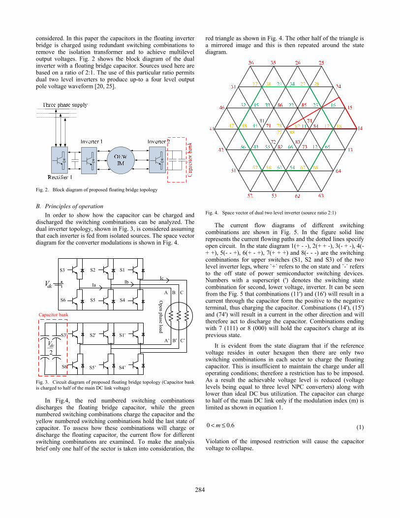
considered. In this paper the capacitors in the floating inverter bridge is charged using redundant switching combinations to remove the isolation transformer and to achieve multilevel output voltages. Fig. 2 shows the block diagram of the dual inverter with a floating bridge capacitor. Sources used here are based on a ratio of 2:1. The use of this particular ratio permits dual two level inverters to produce up-to a four level output pole voltage waveform [20, 25].
Fig. 2. Block diagram of proposed floating bridge topology
B. Principles of operation In order to show how the capacitor can be charged and
discharged the switching combinations can be analyzed. The dual inverter topology, shown in Fig. 3, is considered assuming that each inverter is fed from isolated sources. The space vector diagram for the converter modulations is shown in Fig. 4.
Open phase load
S3 S2 S1
S6 S5 S4
S3' S2' S1'
S6’ S5’ S4’
dcVA
A’
B
B’
C
C’
2dcV
Capacitor bank
Ia IbIc
Fig. 3. Circuit diagram of proposed floating bridge topology (Capacitor bank is charged to half of the main DC link voltage)
In Fig.4, the red numbered switching combinations discharges the floating bridge capacitor, while the green numbered switching combinations charge the capacitor and the yellow numbered switching combinations hold the last state of capacitor. To assess how these combinations will charge or discharge the floating capacitor, the current flow for different switching combinations are examined. To make the analysis brief only one half of the sector is taken into consideration, the
red triangle as shown in Fig. 4. The other half of the triangle is a mirrored image and this is then repeated around the state diagram.
Fig. 4. Space vector of dual two level inverter (source ratio 2:1)
The current flow diagrams of different switching combinations are shown in Fig. 5. In the figure solid line represents the current flowing paths and the dotted lines specify open circuit. In the state diagram 1(+ - -), 2(+ + -), 3(- + -), 4(- + +), 5(- - +), 6(+ - +), 7(+ + +) and 8(- - -) are the switching combinations for upper switches (S1, S2 and S3) of the two level inverter legs, where `+` refers to the on state and `-` refers to the off state of power semiconductor switching devices. Numbers with a superscript (') denotes the switching state combination for second, lower voltage, inverter. It can be seen from the Fig. 5 that combinations (11') and (16') will result in a current through the capacitor form the positive to the negative terminal, thus charging the capacitor. Combinations (14'), (15') and (74') will result in a current in the other direction and will therefore act to discharge the capacitor. Combinations ending with 7 (111) or 8 (000) will hold the capacitor's charge at its previous state.
It is evident from the state diagram that if the reference voltage resides in outer hexagon then there are only two switching combinations in each sector to charge the floating capacitor. This is insufficient to maintain the charge under all operating conditions; therefore a restriction has to be imposed. As a result the achievable voltage level is reduced (voltage levels being equal to three level NPC converters) along with lower than ideal DC bus utilization. The capacitor can charge to half of the main DC link only if the modulation index (m) is limited as shown in equation 1.
6.00 ≤< m (1)
Violation of the imposed restriction will cause the capacitor voltage to collapse.
284
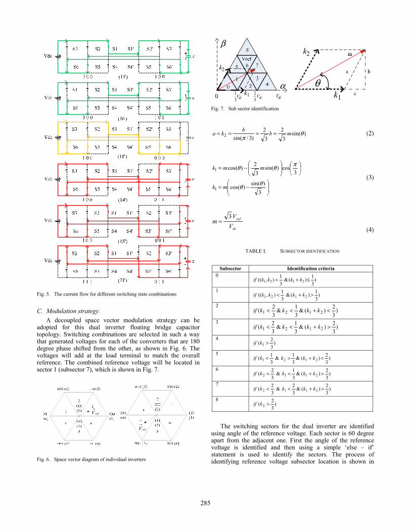
Fig. 5. The current flow for different switching state combinations
C. Modulation strategy A decoupled space vector modulation strategy can be
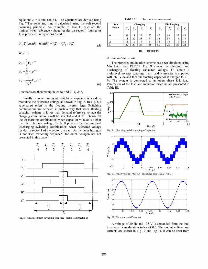
adopted for this dual inverter floating bridge capacitor topology. Switching combinations are selected in such a way that generated voltages for each of the converters that are 180 degree phase shifted from the other, as shown in Fig. 6. The voltages will add at the load terminal to match the overall reference. The combined reference voltage will be located in sector 1 (subsector 7), which is shown in Fig. 7.
refV→
refV→
Fig. 6. Space vector diagram of individual inverters
α
β
1k
2k
θ1k
2k
dcV31
dcV32
dcV
Fig. 7. Sub sector identification
)sin(3
23
2)3/sin(2 θ
πmbbka ==== (2)
⎟⎟⎠
⎞⎜⎜⎝
⎛−=
⎟⎠
⎞⎜⎝
⎛⎟⎟⎠
⎞⎜⎜⎝
⎛−=
3)sin()cos(
3cos)sin(
32)cos(
1
1
θθ
πθθ
mk
mmk
(3)
dc
ref
VV
m3
= (4)
TABLE I. SUBSECTOR IDENTIFICATION
Subsector Identification criteria
0 )
31)(&
31),(( 2121 ≤+< kkkkif
1
)31)(&
31),(( 2121 >+< kkkkif
2
)32)(&
31&
32( 2121 <+<< kkkkif
3 )
32)(&
31&
32( 2121 >+<< kkkkif
4 )
32( 1 >kif
5 )
32)(&
31&
31( 2121 <+>< kkkkif
6 )
32)(&
31&
32( 2112 >+<< kkkkif
7 )
32)(&
32&
32( 2112 >+<< kkkkif
8 )
32( 2 >kif
The switching sectors for the dual inverter are identified using angle of the reference voltage. Each sector is 60 degree apart from the adjacent one. First the angle of the reference voltage is identified and then using a simple ‘else – if’ statement is used to identify the sectors. The process of identifying reference voltage subsector location is shown in
285
equations 2 to 4 and Table I. The equations are derived using Fig. 7.The switching time is calculated using the volt second balancing principle. An example of how to calculate the timings when reference voltage resides on sector 1 (subsector 1) is presented in equations 5 and 6.
332211))sin()(cos( TVTVTViTV sref ++=− θθ (5)
Where,
303
602
01
332
9292
jdc
jdc
jdc
eVV
eVV
eVV
=
=
=
(6)
Equations are then manipulated to find 321 &, TTT
Finally, a seven segment switching sequence is used to modulate the reference voltage as shown in Fig. 8. In Fig. 8 a superscript refers to the floating inverter legs. Switching combinations are selected in such a way that when floating capacitor voltage is lower than demand reference voltage the charging combinations will be selected and it will choose all the discharging combinations when capacitor voltage is higher than the reference voltage. Table II presents the charging and discharging switching combinations when reference voltage resides in sector 1 of the vector diagram. As the outer hexagon is not used switching sequences for outer hexagon are not presented in this paper.
4aT
2bT
2cT
2aT
2cT
2bT
4aT
sT2sT
2sT
Fig. 8. Seven segment switching sequence (sector 1, subsector 1)
TABLE II. SWITCHING COMBINATIONS
Sub Sector
Charging Discharging
aT
bT
cT aT aT bT cT
aT
0 88 11 22 77 87 84 85 88 1 11 22 23 74 84 85 16 74 2 11 16 17 84 84 16 17 84 5 22 23 27 85 85 23 27 22
III. RESULTS
A. Simulation results The proposed modulation scheme has been simulated using
MATLAB and PLECS. Fig. 9 shows the charging and discharging of floating capacitor voltage. To obtain a multilevel inverter topology main bridge inverter is supplied with 260 V dc and then the floating capacitor is charged to 130 V. The system is connected to an open phase R-L load. Parameters of the load and induction machine are presented in Table III.
Fig. 9. Charging and discharging of capacitor
Fig. 10. Phase voltage (Phase A - measured across AA’ Fig. 3)
Fig. 11. Phase current (Phase A)
A voltage of 30 Hz and 135 V is demanded from the dual inverter at a modulation index of 0.6. The output voltage and currents are shown in Fig 10 and Fig 11. It can be seen from
286
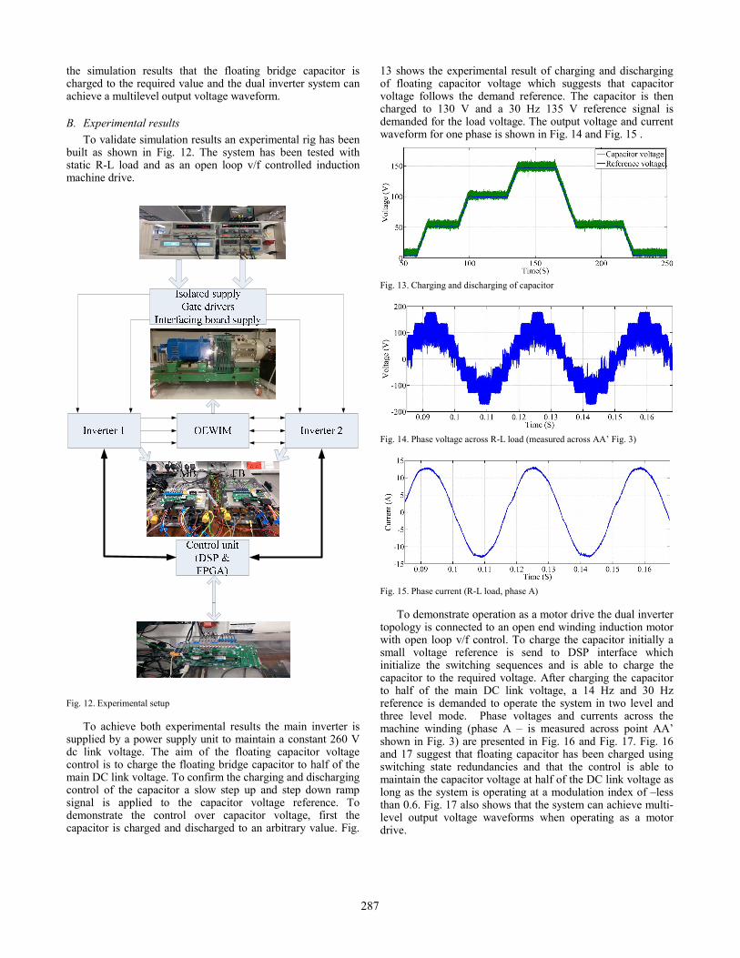
the simulation results that the floating bridge capacitor is charged to the required value and the dual inverter system can achieve a multilevel output voltage waveform.
B. Experimental results To validate simulation results an experimental rig has been
built as shown in Fig. 12. The system has been tested with static R-L load and as an open loop v/f controlled induction machine drive.
Fig. 12. Experimental setup
To achieve both experimental results the main inverter is supplied by a power supply unit to maintain a constant 260 V dc link voltage. The aim of the floating capacitor voltage control is to charge the floating bridge capacitor to half of the main DC link voltage. To confirm the charging and discharging control of the capacitor a slow step up and step down ramp signal is applied to the capacitor voltage reference. To demonstrate the control over capacitor voltage, first the capacitor is charged and discharged to an arbitrary value. Fig.
13 shows the experimental result of charging and discharging of floating capacitor voltage which suggests that capacitor voltage follows the demand reference. The capacitor is then charged to 130 V and a 30 Hz 135 V reference signal is demanded for the load voltage. The output voltage and current waveform for one phase is shown in Fig. 14 and Fig. 15 .
Fig. 13. Charging and discharging of capacitor
Fig. 14. Phase voltage across R-L load (measured across AA’ Fig. 3)
Fig. 15. Phase current (R-L load, phase A)
To demonstrate operation as a motor drive the dual inverter topology is connected to an open end winding induction motor with open loop v/f control. To charge the capacitor initially a small voltage reference is send to DSP interface which initialize the switching sequences and is able to charge the capacitor to the required voltage. After charging the capacitor to half of the main DC link voltage, a 14 Hz and 30 Hz reference is demanded to operate the system in two level and three level mode. Phase voltages and currents across the machine winding (phase A – is measured across point AA’ shown in Fig. 3) are presented in Fig. 16 and Fig. 17. Fig. 16 and 17 suggest that floating capacitor has been charged using switching state redundancies and that the control is able to maintain the capacitor voltage at half of the DC link voltage as long as the system is operating at a modulation index of –less than 0.6. Fig. 17 also shows that the system can achieve multi-level output voltage waveforms when operating as a motor drive.
287
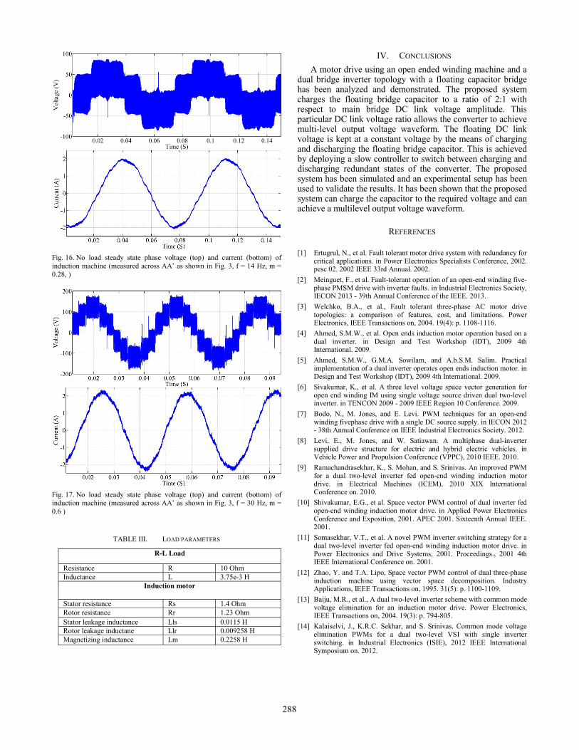
Fig. 16. No load steady state phase voltage (top) and current (bottom) of induction machine (measured across AA’ as shown in Fig. 3, f = 14 Hz, m = 0.28, )
Fig. 17. No load steady state phase voltage (top) and current (bottom) of induction machine (measured across AA’ as shown in Fig. 3, f = 30 Hz, m = 0.6 )
TABLE III. LOAD PARAMETERS
R-L Load
Resistance R 10 Ohm Inductance L 3.75e-3 H
Induction motor
Stator resistance Rs 1.4 Ohm Rotor resistance Rr 1.23 Ohm Stator leakage inductance Lls 0.0115 H Rotor leakage inductane Llr 0.009258 H Magnetizing inductance Lm 0.2258 H
IV. CONCLUSIONS A motor drive using an open ended winding machine and a
dual bridge inverter topology with a floating capacitor bridge has been analyzed and demonstrated. The proposed system charges the floating bridge capacitor to a ratio of 2:1 with respect to main bridge DC link voltage amplitude. This particular DC link voltage ratio allows the converter to achieve multi-level output voltage waveform. The floating DC link voltage is kept at a constant voltage by the means of charging and discharging the floating bridge capacitor. This is achieved by deploying a slow controller to switch between charging and discharging redundant states of the converter. The proposed system has been simulated and an experimental setup has been used to validate the results. It has been shown that the proposed system can charge the capacitor to the required voltage and can achieve a multilevel output voltage waveform.
REFERENCES [1] Ertugrul, N., et al. Fault tolerant motor drive system with redundancy for
critical applications. in Power Electronics Specialists Conference, 2002. pesc 02. 2002 IEEE 33rd Annual. 2002.
[2] Meinguet, F., et al. Fault-tolerant operation of an open-end winding five-phase PMSM drive with inverter faults. in Industrial Electronics Society, IECON 2013 - 39th Annual Conference of the IEEE. 2013.
[3] Welchko, B.A., et al., Fault tolerant three-phase AC motor drive topologies: a comparison of features, cost, and limitations. Power Electronics, IEEE Transactions on, 2004. 19(4): p. 1108-1116.
[4] Ahmed, S.M.W., et al. Open ends induction motor operation based on a dual inverter. in Design and Test Workshop (IDT), 2009 4th International. 2009.
[5] Ahmed, S.M.W., G.M.A. Sowilam, and A.b.S.M. Salim. Practical implementation of a dual inverter operates open ends induction motor. in Design and Test Workshop (IDT), 2009 4th International. 2009.
[6] Sivakumar, K., et al. A three level voltage space vector generation for open end winding IM using single voltage source driven dual two-level inverter. in TENCON 2009 - 2009 IEEE Region 10 Conference. 2009.
[7] Bodo, N., M. Jones, and E. Levi. PWM techniques for an open-end winding fivephase drive with a single DC source supply. in IECON 2012 - 38th Annual Conference on IEEE Industrial Electronics Society. 2012.
[8] Levi, E., M. Jones, and W. Satiawan. A multiphase dual-inverter supplied drive structure for electric and hybrid electric vehicles. in Vehicle Power and Propulsion Conference (VPPC), 2010 IEEE. 2010.
[9] Ramachandrasekhar, K., S. Mohan, and S. Srinivas. An improved PWM for a dual two-level inverter fed open-end winding induction motor drive. in Electrical Machines (ICEM), 2010 XIX International Conference on. 2010.
[10] Shivakumar, E.G., et al. Space vector PWM control of dual inverter fed open-end winding induction motor drive. in Applied Power Electronics Conference and Exposition, 2001. APEC 2001. Sixteenth Annual IEEE. 2001.
[11] Somasekhar, V.T., et al. A novel PWM inverter switching strategy for a dual two-level inverter fed open-end winding induction motor drive. in Power Electronics and Drive Systems, 2001. Proceedings., 2001 4th IEEE International Conference on. 2001.
[12] Zhao, Y. and T.A. Lipo, Space vector PWM control of dual three-phase induction machine using vector space decomposition. Industry Applications, IEEE Transactions on, 1995. 31(5): p. 1100-1109.
[13] Baiju, M.R., et al., A dual two-level inverter scheme with common mode voltage elimination for an induction motor drive. Power Electronics, IEEE Transactions on, 2004. 19(3): p. 794-805.
[14] Kalaiselvi, J., K.R.C. Sekhar, and S. Srinivas. Common mode voltage elimination PWMs for a dual two-level VSI with single inverter switching. in Industrial Electronics (ISIE), 2012 IEEE International Symposium on. 2012.
288
[15] Casadei, D., et al., Multilevel Operation and Input Power Balancing for a Dual Two-Level Inverter with Insulated DC Sources. Industry Applications, IEEE Transactions on, 2008. 44(6): p. 1815-1824.
[16] Casadei, D., et al. Switching Technique for Dual-Two level Inverter Supplied by Two Separate Sources. in Applied Power Electronics Conference, APEC 2007 - Twenty Second Annual IEEE. 2007.
[17] Grandi, G. and D. Ostojic. Dual inverter space vector modulation with power balancing capability. in EUROCON 2009, EUROCON '09. IEEE. 2009.
[18] Grandi, G., et al. Power balancing of a multilevel converter with two insulated supplies for three-phase six-wire loads. in Power Electronics and Applications, 2005 European Conference on. 2005.
[19] Grandi, G., et al. Multilevel Operation of a Dual Two-Level Inverter with Power Balancing Capability. in Industry Applications Conference, 2006. 41st IAS Annual Meeting. Conference Record of the 2006 IEEE. 2006.
[20] Lega, A., Multilevel converters: Dual two-level inverter scheme, in department of electrical engineering. 2007, University of Bologna: Bologna, Italy
[21] Junha, K., J. Jinhwan, and N. Kwanghee, Dual-inverter control strategy for high-speed operation of EV induction motors. Industrial Electronics, IEEE Transactions on, 2004. 51(2): p. 312-320.
[22] Ewanchuk, J. and J. Salmon. A Square-wave Controller for a high speed induction motor drive using a three phase floating bridge inverter. in Energy Conversion Congress and Exposition (ECCE), 2010 IEEE. 2010.
[23] Haque, R.U., et al. PWM control of a dual inverter drive using an open-ended winding induction motor. in Applied Power Electronics Conference and Exposition (APEC), 2013 Twenty-Eighth Annual IEEE. 2013.
[24] Ewanchuk, J., J. Salmon, and C. Chapelsky, A Method for Supply Voltage Boosting in an Open-Ended Induction Machine Using a Dual Inverter System With a Floating Capacitor Bridge. Power Electronics, IEEE Transactions on, 2013. 28(3): p. 1348-1357.
[25] Reddy, B.V. and V.T. Somasekhar, A Dual Inverter Fed Four-Level Open-End Winding Induction Motor Drive With a Nested Rectifier-Inverter. Industrial Informatics, IEEE Transactions on, 2013. 9(2): p. 938-946.
289