Embed Size (px)
Citation preview
Progress In Electromagnetics Research M, Vol. 30, 39–50, 2013
A DUAL-BAND TERAHERTZ METAMATERIAL BASEDON A HYBRID ‘H’-SHAPED CELL
Wanyi Guo1, 2, *, Lianxing He1, Hao Sun1, Hongwei Zhao3,Biao Li4, and Xiao-Wei Sun1
1Key Laboratory of Terahertz Solid-State Technology, ShanghaiInstitute of Microsystem and Information Technology, Shanghai200050, China2Graduate University of the Chinese Academy of Sciences, Beijing100049, China3Shanghai Institute of Applied Physics, Shanghai 201800, China4National Laboratory of Antennas and Microwave Technology, XidianUniversity, Xi’an, Shaanxi 710071, China
Abstract—We present a dualband terahertz metamaterial basedon a hybrid ‘H’-shaped cell of different sizes. The proposed ‘H’-shaped metamaterial (HSM) structure, fabricated on a quartz (SiO2)substrate, exhibits two intense electrical resonances at ∼0.95THzand ∼1.26THz, respectively. Extracted effective permittivity shownegative values in 0.95–1.01 THz and 1.26–1.42 THz bands. Measuredresults from the terahertz time-domain spectroscopy (THz-TDS)experiments show good agreement with the simulated results.
1. INTRODUCTION
Electromagnetic (EM) metamaterials are fascinating artificial compos-ites with embedded sub-wavelength metallic structures [1, 2]. Since thefirst experimental realization of THz metamaterial reported by Yen etal. in 2004 [3], metamaterials with negative permittivity and/or per-meability have spurred a significant research interest in THz regimedue to their exotic EM properties that are not readily available fromconventional materials [4, 5]. The THz metamaterials have enabled thedevelopment of new devices possible utilization in many novel appli-cations in THz regime, where most natural materials behave too weak
Received 14 January 2013, Accepted 19 March 2013, Scheduled 19 March 2013* Corresponding author: Wanyi Guo ([email protected]).
40 Guo et al.
EM response to be used. For example, a metamaterial solid-state ter-ahertz phase modulator was presented by Chen et al. in 2009 [6]. Aperfect metamaterial absorber based on a split-ring-cross resonator wasdesigned by Cheng et al. in 2010 [7]. And Choi et al. present a terahertzmetamaterial with unnaturally refractive index in 2011 [8]. However,the operation of many reported THz metamaterials often exhibits EMinteraction to THz wave in a single and narrow frequency band, becom-ing a major hurdle to realize the possible multi-band THz functionaldevices such as modulators, switchers, filters, molecular sensors, ab-sorbers and so on. Realizing multi-band operation of metamaterials,especially in the THz regime, has thus attracted a strong research inter-est. Recently, a few works about dualband and multi-band THz meta-materials have been reported [9–18]. A double band left-handed meta-material composed of an extended version of the S-shaped resonatorsat microwave frequencies was presented by Chen et al. in 2004 [9]. In2006, Gorkunov et al. suggest double-resonant (binary) metamaterialscomposed of two types of magnetic resonant elements [11]. Ekmekci etal. proposed the micro-split SRR type unit cell structures to be usedfor multi-band and tunable metamaterial design in 2009 [15]. Ma etal. reported a novel dual band THz metamaterial based on a singlepatterned layer in 2011 [17]. And a dualband metamaterial absorberbased with resonant-magnetic structures was presented by Lee and Leein 2012 [18].
In this letter, we present a simple design of dualband THzmetamaterial based on a hybrid hollow ‘H’-shaped sub-wavelengthstructure. The proposed ‘H’-shaped metamaterial (HSM), embeddedwith periodic ‘H’-shaped metallic rings in the quartz substrate,performs two distinct electric resonances at ∼0.95THz and ∼1.26 THz.Negative values of permittivity in 0.95–1.01 THz and 1.26–1.42 THzbands are achieved.
2. DESIGN AND ANALYSES
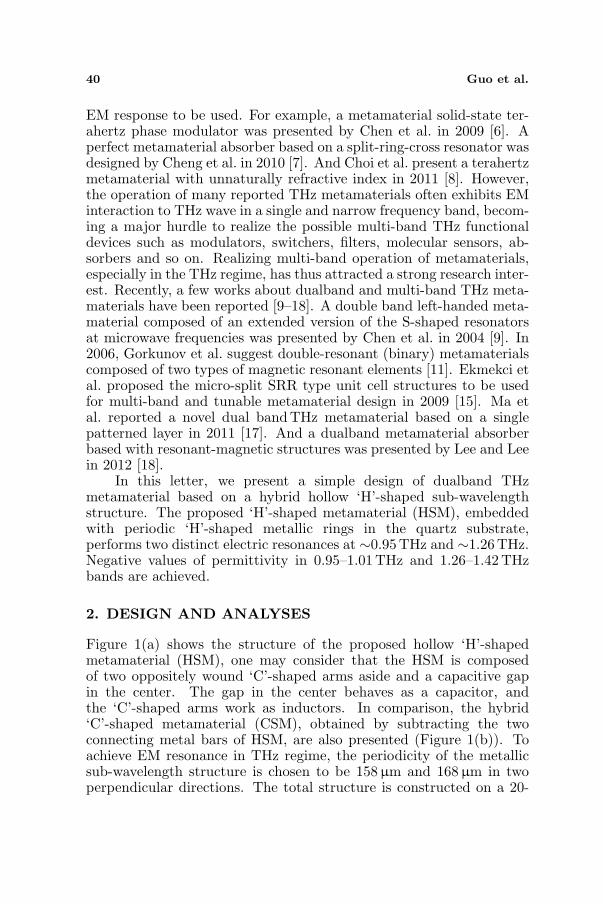
Figure 1(a) shows the structure of the proposed hollow ‘H’-shapedmetamaterial (HSM), one may consider that the HSM is composedof two oppositely wound ‘C’-shaped arms aside and a capacitive gapin the center. The gap in the center behaves as a capacitor, andthe ‘C’-shaped arms work as inductors. In comparison, the hybrid‘C’-shaped metamaterial (CSM), obtained by subtracting the twoconnecting metal bars of HSM, are also presented (Figure 1(b)). Toachieve EM resonance in THz regime, the periodicity of the metallicsub-wavelength structure is chosen to be 158µm and 168µm in twoperpendicular directions. The total structure is constructed on a 20-
Progress In Electromagnetics Research M, Vol. 30, 2013 41
(a) (b)
Figure 1. The designed structures of HSM and CSM. (a) HSM.(b) CSM.
µm-thick quartz (SiO2) substrate, whose dielectric constant ε and losstangent tanδ are 3.78 and 0.001, respectively. And the metal arraylayer is gold with thickness of 300nm. The THz EM wave propagatesat normal incidence (k in Figure 1) with the electric and magnetic fieldscompletely parallel to the plane of metal layers. And the polarizationof electric field is perpendicular to the gap between the two ‘C’-shaped arms. The finite element-based commercial electromagneticfield solver Ansoft HFSS is used for the simulation and optimizationof the proposed structure. The optimized geometrical sizes of theproposed sub-wavelength structures in Figure 1 are: W = 5µm,D = 5µm, L1 = 15µm, L2 = 10µm, L3 = 20µm, A1 = 55µm,A2 = 55µm, B2 = 35µm.
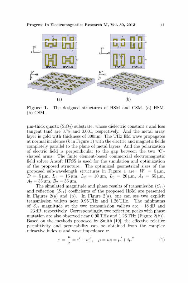
The simulated magnitude and phase results of transmission (S21)and reflection (S11) coefficients of the proposed HSM are presentedin Figures 2(a) and (b). In Figure 2(a), one can see two explicittransmission valleys near 0.95 THz and 1.26 THz. The minimumsof S21 magnitude at the two transmission valleys are −18 dB and−23 dB, respectively. Correspondingly, two reflection peaks with phasemutation are also observed near 0.95 THz and 1.26 THz (Figure 2(b)).Based on the methods proposed by Smith [19], the effective relativepermittivity and permeability can be obtained from the complexrefractive index n and wave impedance z:
ε =n
z= ε′ + iε′′, µ = nz = µ′ + iµ′′ (1)
42 Guo et al.
n =1kd
cos−1
[1
2S21
(1− S2
11 + S221
)](2)
z =
√(1 + S11)
2 − S221
(1− S11)2 − S221
(3)
(a) (b)
(c) (d)
(e) (f)
Figure 2. (a) Magnitude and phase of transmission (S21) forHSM. (b) Magnitude and phase of reflection (S11) for HSM. (c)Effective permittivity of HSM. (d) Effective permeability of HSM. (e)Magnitudes of transmission (S21) of HSM and CSM. (f) Real parts ofeffective permittivity of HSM and CSM.
Progress In Electromagnetics Research M, Vol. 30, 2013 43
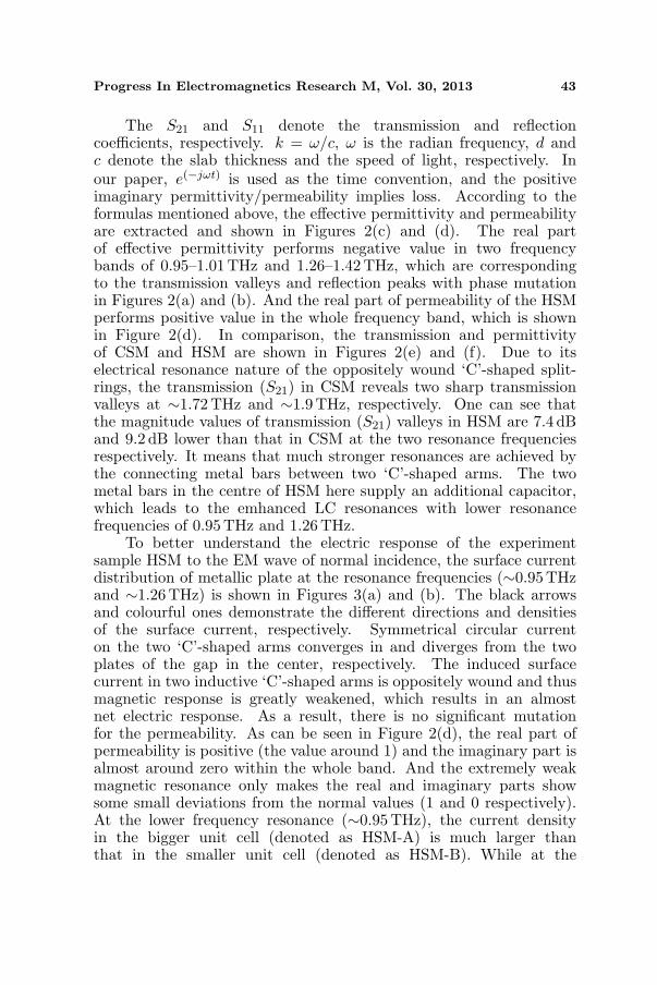
The S21 and S11 denote the transmission and reflectioncoefficients, respectively. k = ω/c, ω is the radian frequency, d andc denote the slab thickness and the speed of light, respectively. Inour paper, e(−jωt) is used as the time convention, and the positiveimaginary permittivity/permeability implies loss. According to theformulas mentioned above, the effective permittivity and permeabilityare extracted and shown in Figures 2(c) and (d). The real partof effective permittivity performs negative value in two frequencybands of 0.95–1.01THz and 1.26–1.42 THz, which are correspondingto the transmission valleys and reflection peaks with phase mutationin Figures 2(a) and (b). And the real part of permeability of the HSMperforms positive value in the whole frequency band, which is shownin Figure 2(d). In comparison, the transmission and permittivityof CSM and HSM are shown in Figures 2(e) and (f). Due to itselectrical resonance nature of the oppositely wound ‘C’-shaped split-rings, the transmission (S21) in CSM reveals two sharp transmissionvalleys at ∼1.72 THz and ∼1.9THz, respectively. One can see thatthe magnitude values of transmission (S21) valleys in HSM are 7.4 dBand 9.2 dB lower than that in CSM at the two resonance frequenciesrespectively. It means that much stronger resonances are achieved bythe connecting metal bars between two ‘C’-shaped arms. The twometal bars in the centre of HSM here supply an additional capacitor,which leads to the emhanced LC resonances with lower resonancefrequencies of 0.95THz and 1.26 THz.
To better understand the electric response of the experimentsample HSM to the EM wave of normal incidence, the surface currentdistribution of metallic plate at the resonance frequencies (∼0.95THzand ∼1.26THz) is shown in Figures 3(a) and (b). The black arrowsand colourful ones demonstrate the different directions and densitiesof the surface current, respectively. Symmetrical circular currenton the two ‘C’-shaped arms converges in and diverges from the twoplates of the gap in the center, respectively. The induced surfacecurrent in two inductive ‘C’-shaped arms is oppositely wound and thusmagnetic response is greatly weakened, which results in an almostnet electric response. As a result, there is no significant mutationfor the permeability. As can be seen in Figure 2(d), the real part ofpermeability is positive (the value around 1) and the imaginary part isalmost around zero within the whole band. And the extremely weakmagnetic resonance only makes the real and imaginary parts showsome small deviations from the normal values (1 and 0 respectively).At the lower frequency resonance (∼0.95THz), the current densityin the bigger unit cell (denoted as HSM-A) is much larger thanthat in the smaller unit cell (denoted as HSM-B). While at the
44 Guo et al.
(a) HSM 0.95 THz (b) HSM 1.26 THz
(c) HSM 0.95 THz (d) HSM 1.26 THz
Figure 3. (a) Surface current distribution of HSM at 0.95 THz.(b) Surface current distribution of HSM at 1.26 THz. (c) Surfaceelectric field distribution of HSM at 0.95 THz. (d) Surface electricfield distribution of HSM at 1.26THz.
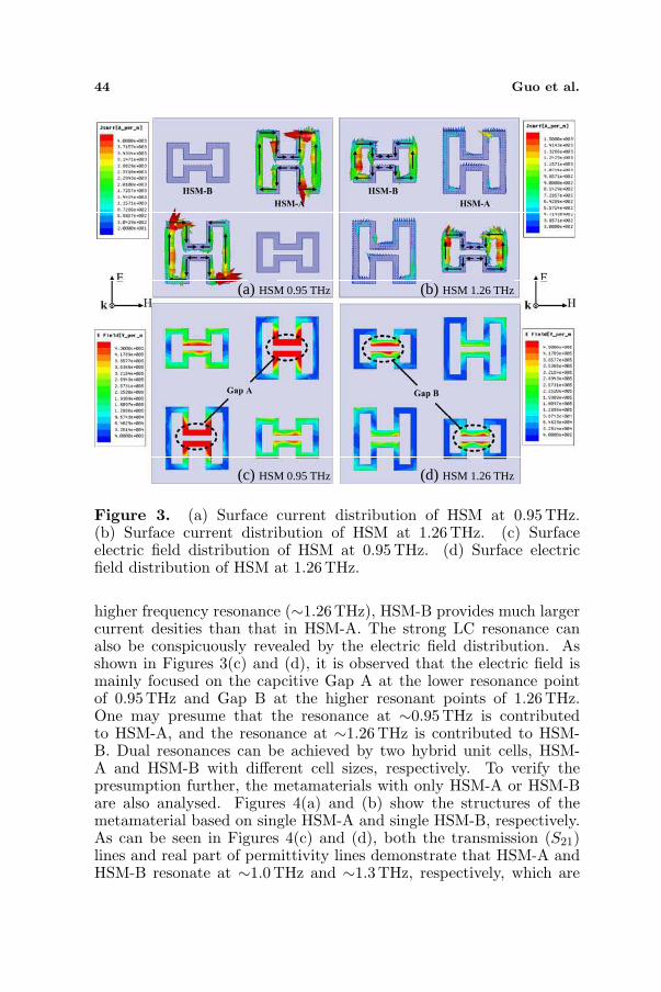
higher frequency resonance (∼1.26THz), HSM-B provides much largercurrent desities than that in HSM-A. The strong LC resonance canalso be conspicuously revealed by the electric field distribution. Asshown in Figures 3(c) and (d), it is observed that the electric field ismainly focused on the capcitive Gap A at the lower resonance pointof 0.95 THz and Gap B at the higher resonant points of 1.26 THz.One may presume that the resonance at ∼0.95THz is contributedto HSM-A, and the resonance at ∼1.26THz is contributed to HSM-B. Dual resonances can be achieved by two hybrid unit cells, HSM-A and HSM-B with different cell sizes, respectively. To verify thepresumption further, the metamaterials with only HSM-A or HSM-Bare also analysed. Figures 4(a) and (b) show the structures of themetamaterial based on single HSM-A and single HSM-B, respectively.As can be seen in Figures 4(c) and (d), both the transmission (S21)lines and real part of permittivity lines demonstrate that HSM-A andHSM-B resonate at ∼1.0THz and ∼1.3THz, respectively, which are
Progress In Electromagnetics Research M, Vol. 30, 2013 45
(a) HSM-A (b) HSM-B
(c) Transmission (d) Real part of permittivity
Figure 4. (a) Structure of HSM-A. (b) Structure of HSM-B.(c) Simulated transmission lines of HSM-A, HSM-B and HSM. (d) Realpart of permittivity of HSM-A, HSM-B, and HSM.
reasonably agreed with the two resonances in HSM. So we can saythat the two distinct resonances in HSM are really originated fromHSM-A (the bigger cell) and HSM-B(the smaller cell), respectively.
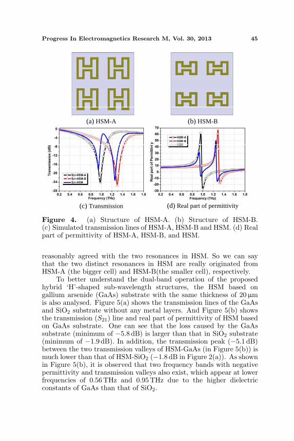
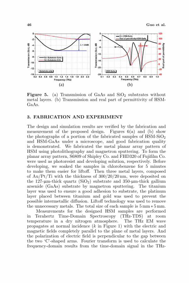
To better understand the dual-band operation of the proposedhybrid ‘H’-shaped sub-wavelength structures, the HSM based ongallium arsenide (GaAs) substrate with the same thickness of 20µmis also analysed. Figure 5(a) shows the transmission lines of the GaAsand SiO2 substrate without any metal layers. And Figure 5(b) showsthe transmission (S21) line and real part of permittivity of HSM basedon GaAs substrate. One can see that the loss caused by the GaAssubstrate (minimum of −5.8 dB) is larger than that in SiO2 substrate(minimum of −1.9 dB). In addition, the transmission peak (−5.1 dB)between the two transmission valleys of HSM-GaAs (in Figure 5(b)) ismuch lower than that of HSM-SiO2 (−1.8 dB in Figure 2(a)). As shownin Figure 5(b), it is observed that two frequency bands with negativepermittivity and transmission valleys also exist, which appear at lowerfrequencies of 0.56 THz and 0.95 THz due to the higher dielectricconstants of GaAs than that of SiO2.
46 Guo et al.
(a) (b)
Figure 5. (a) Transmission of GaAs and SiO2 substrates withoutmetal layers. (b) Transmission and real part of permittivity of HSM-GaAs.
3. FABRICATION AND EXPERIMENT
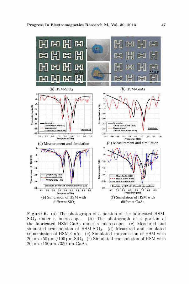
The design and simulation results are verified by the fabrication andmeasurement of the proposed design. Figures 6(a) and (b) showthe photographs of a portion of the fabricated samples of HSM-SiO2
and HSM-GaAs under a microscope, and good fabrication qualityis demonstrated. We fabricated the metal planar array pattern ofHSM using photolithography and magnetron sputtering. To form theplanar array pattern, S6809 of Shipley Co. and FHD320 of Fujifilm Co.were used as photoresist and developing solution, respectively. Beforedeveloping, we soaked the samples in chlorobenzene for 5 minutesto make them easier for liftoff. Then three metal layers, composedof Au/Pt/Ti with the thickness of 300/20/20 nm, were deposited onthe 127-µm-thick quartz (SiO2) substrate and 350-µm-thick galliumarsenide (GaAs) substrate by magnetron sputtering. The titaniumlayer was used to ensure a good adhesion to substrate, the platinumlayer placed between titanium and gold was used to prevent thepossible intermetallic diffusion. Liftoff technology was used to removethe unnecessary metals. The total size of each sample is 5 mm ∗ 5mm.
Measurements for the designed HSM samples are performedin Terahertz Time-Domain Spectroscopy (THz-TDS) at roomtemperature in a dry nitrogen atmosphere. The THz EM wavepropagates at normal incidence (k in Figure 1) with the electric andmagnetic fields completely parallel to the plane of metal layers. Andthe polarization of electric field is perpendicular to the gap betweenthe two ‘C’-shaped arms. Fourier transform is used to calculate thefrequency-domain results from the time-domain signal in the THz-
Progress In Electromagnetics Research M, Vol. 30, 2013 47
(a) HSM-SiO (b) HSM-GaAs
(c) Measurement and simulation (d) Measurement and simulation
(e) Simulation of HSM with
2
different SiO2
(f) Simulation of HSM withdifferent GaAs
Figure 6. (a) The photograph of a portion of the fabricated HSM-SiO2 under a microscope. (b) The photograph of a portion ofthe fabricated HSM-GaAs under a microscope. (c) Measured andsimulated transmission of HSM-SiO2. (d) Measured and simulatedtransmission of HSM-GaAs. (e) Simulated transmission of HSM with20µm-/50µm-/100µm-SiO2. (f) Simulated transmission of HSM with20µm-/150µm-/350µm-GaAs.
48 Guo et al.
TDS experiments. The measured and simulated transmissions forthe designed HSM samples to THz wave are plotted in Figures 6(c)and (d). As for the two main transmission valleys, one can see thatgood agreements between the measured and simulated results for bothof the HSM-SiO2 and HSM-GaAs samples are achieved.
As shown in Figures 6(e) and (f), the simulated transmissionspectra of HSM with different thicknesses substrates are similar excepta few ripples. The ripples in the transmission spectra come fromthe Fabry-Perot resonances [20, 21], which are caused by the internalreflections within the two surfaces in the direction of propagation.And the thicker the substrate is, the lower the Fabry-Perot resonancefrequency is. When studying the metamaterial performance causedby the periodic metal sub-wavelength structure, it is necessary tokeep the Fabry-Perot resonance frequency far away from the designedfrequencies. As a result, we designed and analyzed the HSM on20-µm-thick quartz (SiO2) and gallium arsenide (GaAs) substrateswhose Fabry-Perot resonance frequencies are much higher than theas-designed frequencies. But it is difficult to fabricate the metal arrayson such a thin substrate of 20-µm-thickness and do the measurementwith such thin samples. As a result, considering the fabricationconditions and difficulties in measurement, we fabricated the metallayers with hybrid ‘H’-shaped sub-wavelength structures on the 127-µm-thick quartz (SiO2) substrate and 350-µm-thick GaAs substrate,and then do the measurement successfully. The measured results showgood agreement with the simulated results.
4. CONCLUSIONS
In conclusion, we present the design, fabrication and experiment ofa dual-band terahertz metamaterial based on a hybrid ‘H’-shapedcell with different sizes, and each cell is constructed by connectingtwo oppositely wound ‘C’-shaped arms aside and a capacitive gapin the center. The proposed ‘H’-shaped metamaterial (HSM) basedon a quartz substrate exhibits two intense electrical resonances at∼0.95THz and ∼1.26THz when the THz wave propagates normally tothe metallic array surface and the THz electric field is perpendicularto the split gap (E). Measured results obtained from the THz-TDSexperiments show good agreement with the simulated results. Basedon the strong electric-field-coupling, negative values of permittivityin a two bands 0.95–1.01THz and 1.26–1.42 THz are achieved. Theproposed THz metamaterial could be a meaningful candidate for thepotential multiband THz applications.
Progress In Electromagnetics Research M, Vol. 30, 2013 49
ACKNOWLEDGMENT
This work was supported by the National Basic Research Program ofChina (973) (Grant No. 2009CB320207).
REFERENCES
1. Veselago, V. G., “The electrodynamics of substances withsimultaneously negative values of permittivity and permeability,”Sov. Phys. Usp., Vol. 10, No. 4, 509–514, 1968.
2. Pendry, J. B., A. J. Holden, D. J. Robbins, and W. J. Stewart,“Magnetism from conductors and enhanced nonlinear phenom-ena,” IEEE Trans. Microw. Theory Tech., Vol. 47, No. 11, 2075–2084, 1999.
3. Yen, T. J., W. J. Padilla, N. Fang, D. C. Vier, D. R. Smith,J. B. Pendry, D. N. Basov, and X. Zhang, “Terahertz magneticresponse from artificial materials,” Science, Vol. 303, No. 5663,1494–1496, 2004.
4. Padilla, W. J., A. J. Taylor, C. Highstrete, M. Lee, andR. D. Averott, “Dynamical electric and magnetic metamaterialresponse at terahertz frequencies,” Phys. Rev. Lett., Vol. 96,107401(1)–107401(4), 2006.
5. Tuniz, A., B. T. Kuhlmey, R. Lwin, A. Wang, J. Anthony,R. Leonhardt, and S. C. Fleming, “Drawn metamaterials withplasmonic response at terahertz frequencies,” App. Phys. Lett.,Vol. 96, 191101(1)–191101(3), 2010.
6. Chen, H.-T., W. J. Padilla, M. J. Cich, A. K. Azad, R. D. Averitt,and A. J. Taylor, “A metamaterial solid-state terahertz phasemodulator,” Nature Photonics, Vol. 3, 148–151, 2009.
7. Cheng, Y., H. Yang, Z. Cheng, and N. Wu, “Perfect metamaterialabsorber based on a split-ring-cross resonator,” J. Appl. Phys. A,Vol. 102, 99–103, 2010.
8. Choi, M., S. H. Lee, Y. Kim, S. B. Kang, J. Shin, M. H. Kwak,K.-Y. Kang, Y. Hee, N. Park, and B. Min, “A terhaertzmetamaterial with unnaturally high refractive index,” Nature,Vol. 470, No. 09776, 369–373, 2011.
9. Chen, H.-S., L.-X. Ran, J. Tao, F. Huang, X.-M. Zhang, andK.-S. Chen, “Metamaterial exhibiting left-handed properties overmultiple frequency bands,” J. Appl. Phys., Vol. 96, 5338, 2004.
10. Sydoruk, O., O. Zhuromskyy, E. Shamonina, and L. Solymar,“Phono-like dispersion curves of magnetoinductive waves,” Appl.Phys. Lett., Vol. 87, 072501, 2005.
50 Guo et al.
11. Gorkunov, M. V., L. V. Shadrivov, and Y. S. Kivshar, “Enhancedparametric processes in binary metamaterials,” Appl. Phys. Lett.,Vol. 88, 071912, 2009.
12. Wen, Q. Y., H. W. Zhang, Y. S. Xie, Q. H. Yang, and Y. L. Liu,“Dual band terahertz metamaterial absorber: Design, fabrication,and characterization,” App. Phys. Lett., Vol. 95, 241111(1)–241111(3), 2009.
13. Yu, Y., C. Bingham, T. Tyler, S. Palit, R. Hand, W. J. Padila,N. M. Jokerst, and S. A. Cummer, “A dual-resonant terahertzmetamaterial based on single-particle electric-field-coupled res-onators,” App. Phys. Lett., Vol. 93, No. 19, 19110(1)–19110(3),2008.
14. Yu, Y., C. Bingham, T. Tyler, S. Palit, T. H. Hand, W. J. Padilla,D. R. Smith, N. M. Jokerst, and S. A. Cummer, “Dual-band planarelectric metamaterial in the terahertz regime,” Opt. Express,Vol. 16, No. 13, 9746–9752, 2008.
15. Ekmekci, E., K. Topalli, T. Akin, and G. Turhan-Sayan, “Atunable multi-band metamaterial design using micro-split SRRstructures,” Opt. Express, Vol. 17, No. 18, 16406–16058, 2009.
16. Tao, H., C. M. Bingham, D. Pilon, K. Fan, A. C. Strikwerda,D. Shrekenhamer, W. J. Padilla, X. Zhang, and R. D. Averitt,“A dual band terahertz metamaterial absorber,” J. Appl. Phys.,Vol. 43, 225102–225106, 2010.
17. Ma, Y., Q. Chen, J. Grant, S. C. Saha, A. Khalid, andD. R. S. Cumming, “A terahertz polarization insensitive dual bandmetamaterial absorber,” Opt. Lett., Vol. 36, No. 6, 945–947, 2011.
18. Lee, H.-M. and H.-S. Lee, “A dualband metamaterial absorberbased with resonant-magnetic structures,” Progress In Electro-magnetics Research Letters, Vol. 33, 1–12, 2012.
19. Smith, D. R., D. C. Vier, T. Koschny, and C. M. Soukoulis, “Elec-tromagnetic parameter retrieval from inhomogeneous metamate-rials,” Phys. Rev. E, Vol. 71, 036617(1)–036617(11), 2005.
20. Han, N. R., Z. C. Chen, C. S. Lim, B. Ng, and M. H. Hong,“Broadband multi-layer terahertz metamaterials fabrication andcharacterization on flexible substrates,” Opt. Express, Vol. 19,No. 8, 6991–6998, 2011.
21. Guo, W., L. He, B. Li, T. Teng, and X.-W. Sun, “A widebandand dual-resonant terahertz metamaterial using a modified SRRstructure,” Progress In Electromagnetics Research, Vol. 134, 289–299, 2013.