Embed Size (px)
Citation preview
Purdue UniversityPurdue e-Pubs
ECE Technical Reports Electrical and Computer Engineering
11-1-1992
A Double Self-Aligned Silicon Bipolar TransistorUtilizing Selectively-Grown Single Crystal ExtrinsicContactsJ. L. Glenn Jr.Purdue University School of Electrical Engineering
G. W. NeudeckPurdue University School of Electrical Engineering
Follow this and additional works at: http://docs.lib.purdue.edu/ecetr
This document has been made available through Purdue e-Pubs, a service of the Purdue University Libraries. Please contact [email protected] foradditional information.
Glenn, J. L. Jr. and Neudeck, G. W., "A Double Self-Aligned Silicon Bipolar Transistor Utilizing Selectively-Grown Single CrystalExtrinsic Contacts" (1992). ECE Technical Reports. Paper 267.http://docs.lib.purdue.edu/ecetr/267
TR-EE 92-46 NOVEMBER 1992
A Double Self-Aligned Silicon Bipolar Transistor Utilizing Selectively-Grown
Single Crystal Extrinsic Contacts
J. L. Glenn, Jr. and G. W. Neudeck
School of Electrical Engineering Purdue University
West Lafayette, IN 47907-1285
This research was supported by the Semiconductor Research Corporation Contract # 92-SJ-1018
TABLE OF CONTENTS
Page .. LIST OF TABLES ............................................................................................... vii
... LIST OF FIGWRES ............................................................................................. v ~ i i
.. ABSTRACT ......................................................................................................... xi1
CHAPTER INTRODUCTION
1.1 Research Motivation .................................................................................. 1 1.2 Overview of Proposed Bipolar Transistor ................................................. 2 1.3 Research Overview .................................................................................... 5 1.4 Thesis Overview ........................................................................................ 6
CHAPTER 2 . LITERATURE SURVEY ............................................................... 7
.2.1 Scope and Purpose ..................................................................................... 7
.2.2 Background: Selective Epitaxial Growth (SEG) of Silicon .......................... 7 2.2.1 Formats: SEG, ELO, CLSEG ....................................................... 7
................... 2.2.2 Growth Conditions ...................................... .. 8 2.2.2.1 Preclean ...................................................................... 10 2.2.2.2 Material Quality ........................................................... 11 2.2.2.3 Selectivity .................................................................... 14 2.2.2.4 Reactor Geometry ....................................................... 15
2.2.3 Applications ............................................................................... 16 f!.3 High-speed BJTs (I): Design Considerations ............................................ 18
2.3.1 Transistor Delay ......................................................................... 18 ............................................ 2.3.1.1 Propagation Delay Model 18 ......................................... 2.3.1.2 High-Level Injection Effects 21
2.3.2 Circuit Delay .............................................................................. 24 2.3.2.1 Hybrid-r Circuit Model ............................................... 24
..................................... 2.3.2.2 ECL Circuit Delay Expression 26 ......................................... 2.3.2.3 ECL Power-Delay Relation 28
2.4 High-speed BJTs (11): Design Implementations ....................................... 29 .................................................. 2.4.1 Perspective on LOCOS Isolation 29
2.4.2 Single Self-Aligned Transistors ................................................... 30 2.4.2.1 "SST" Fabrication Sequence ......................................... 30 2.4.2.2 Design Tradeoffs ........................................................... 34 2.4.2.3 Related Structures ...................................................... 35
................................................. 2.4.3 Double Self-Aligned Transistors 36 .................................... 2.4.3.1 'BASIC" Fabrication Sequence 36
2.4.3.2 Design Tradeoffs .......................................................... 38
Page ............................................. 2.4.4 Heterojunction Bipolar Transistors 39
..................................................................... 2.4.4.1 Overview 39 ............................................ 2.4.4.2 Wide Band-Gap Emitters 40
2.4.4.3 Narrow Band-Gap Bases ............................................ 40 ......................... 2.4.5 Scaling Limitations to Polysilicon Technologies 41
................................................................................... 2.5 Chapter Summary 42
............... CHAPTER 3 . PROPOSED BIPOLAR TRANSISTOR STRUCTURE 43
............................................................................................... 3.1 Motivation 43 3.2 Design Drawings ...................................................................................... 44
................................................................................................. 3.3 Discussion 50 ................................... 3.3.1 Scaling of Single-Crystal Silicon Contacts 50
............................................. 3.3.2 P rbcess Advantages/Disadvantages 52 ...................................... 3.3.3 Alternative Emitter Contact Processing 54
3.4 Summary .................................................................................................. 54
CHAPTER 4 . PROCESS DEVELOPMENT ...................................................... 57
4.1 Overview and Purpose ............................................................................. 57 ...................................................................................... 4.2 Processing Tools 57 4.3 Substrate Bipolar Transistors .................................................................. 60
4.3.1 Process Flow ................................................................................ 60 ................................................. 4.3.2 Structural Data and Simulations 62
................................................................ 4.4 Single Self-Aligned Transistors 62 4.4.1 Process Flow ................................................................................ 62
................................................. 4.4.2 Structural Data and Simulations 66 .............................................................. 4.5 Double Self-Aligned Transistors 68
4.5.1 Process Flow ................................................................................ 68 4.5.2 Structural Data and Simulations ................................................. 71
4.6 Resistor Test Structures .......................................................................... 75 4.7 Summary ................................................................................................. 77
(CHAPTER DEVICE CHARACTERISTICS
5.1 Overview and Purpose .............................................................................. 78 ................................................................................... 5.2 Measurement Tools 78
5.3 D.C. Measurements ................................................................................... 79 ............................................................................. 5.3.1 Data Summary 79
............................................ 5.3.2 Forward Active BJT Characteristics 82 ............................................................... 5.3.3 Resistor Test Structures 90
5.4 A.C. Electrical Data of BJTs .................................................................... 90 5.4.1 Emitter/Base Capacitance ........................................................... 90
......................................................... 5.4.2 Collector/Base Capacitance 97 5.5 Summary ................................................................................................. 97
Page
. C I W T E R 6 MODELING OF FULLY SCALED HIGH-SPEED DEVICE ...... 102
6.1 Overview and Purpose ............................................................................ 102 6.2 SUPREM-TV Process Simulations ........................................................... 102
6.2.1 Collector Pedestal Oxidation/RIE ............................................ -103 6.2.2 Complete Device Fabrication ..................................................... 103
6.3 PISCES IIB Electrical Process Emulator ............................................... 106 6.3.1 D.C. Characteristics ................................................................... 106 6.3.2 A.C. Characteristics ................................................................... 110
6.4 Summary ............................................................................................... 115
C I W T E R 7 . CONCLUSIONS ......................................................................... 116
7.1 Summary ................................................................................................ 116 7.2 Future Research ..................................................................................... 117
REFERENCES
LIST OF T m L E S
Table Page
5.1 D.c. electrical data for A1 contacted substrate BJTs (A-sub), polysilicon contacted substrate BJTs (P-sub), SSTs, EL0 base contacted DSTs (E-DST), and polysilicon base contacted DSTs (P-DST), as well as PISCEiS-IIB computer simulations of the self-aligned devices only. Emitter junction areas were 2.4 x 5 0 . 4 ~ r n - ~ and 4.4 x 8 4 . 4 ~ r n - ~ . ............................................. 80
5.2 Area dependent junction leakage currents for devices listed in 'Table 5.1 with emitter areas of 2.4 x 5 0 . 4 ~ r n ~ (type 1) and 4.4 x 8 4 . 4 ~ r n ~ (type 2) ..................................................................................... 81
6.1 Tabular summary of simulated electrical parameters for the plnoposed DST against a comparable SST and non-self-aligned transistor (NSAT) as well as reported values for the SST-1A assuming AE = 0.35 x 5.0 ~ r n ~ 14,101. ......................................................................... 113
viii
LIST OF FIGURES
Figure Page
1.1 Proposed double self-aligned single-crystal silicon contacted bipolar transistor. ........................................................................................................ .4
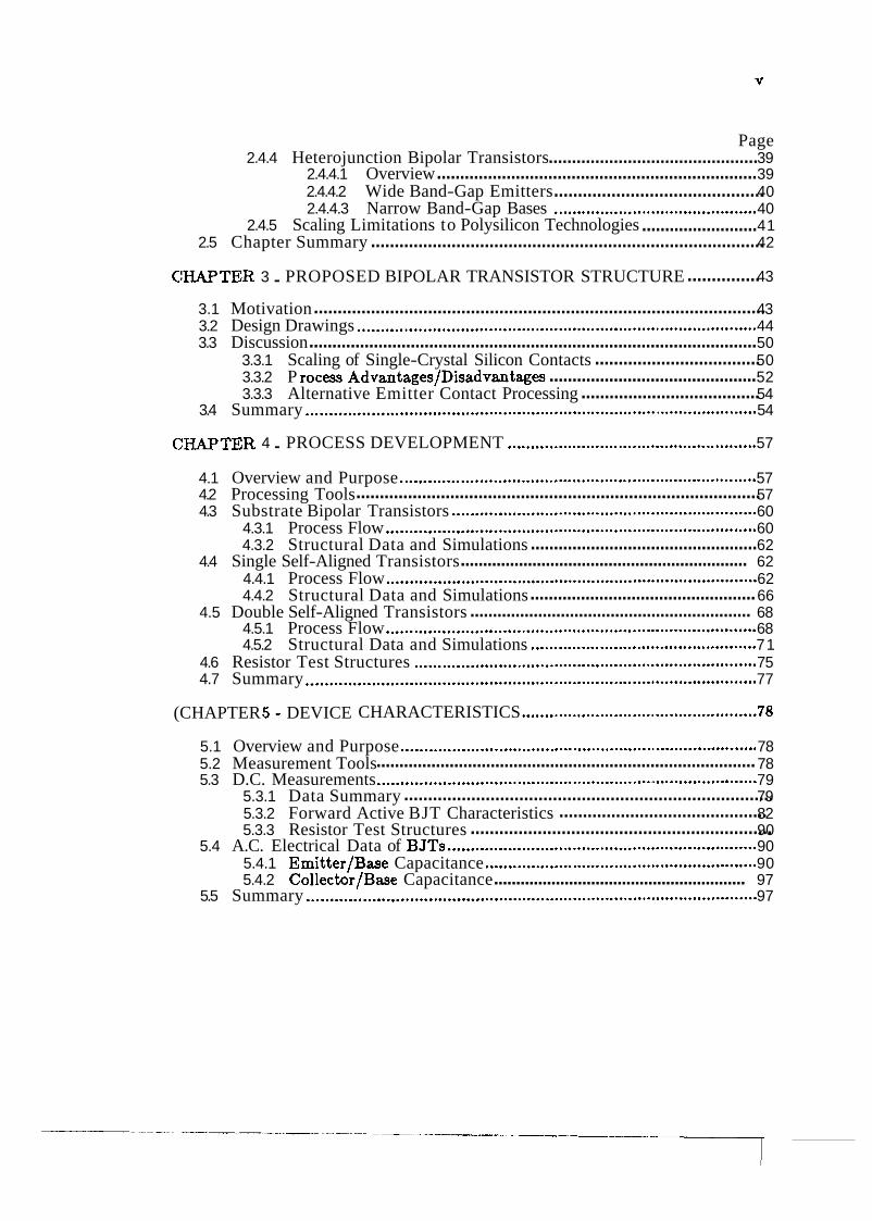
2.1 Cross-sectional drawings showing, (a selective epitaxial growth (SEG), (b) epitaxial lateral overgrowth (EL0 1 , (c) planarized ELO, and (d) confined
...................................................................................... lateral SEG (CLSEG). 9
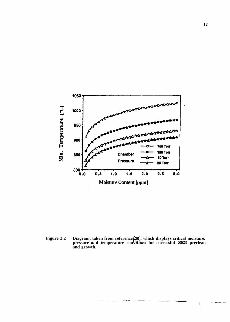
2.2 Diagram, taken from reference [36], which display critical moisture, pressure and temperature conditions for successful SEG preclean and grovvth. ............ 12
2.3 Cross-sectional drawings of (a) the quasi-dielectrically isolated BJT and ......... (b) the bdimensional CMOS inverter fabricated by SEG and EL13 [SO] 17
2.4 Diagram showing the propagation delay through a BJT by (a) d:iagram of transistor and (b) schematic definition of delay terms ................................. 20
2.5 Schematic representation of the variation of transit frequency fT with collector current &. ................................................................................. 22
2.6 Figure defining the influence of Miller capacitance on frequency response; a generalized differential input stage to ECL gate or operational amplifier, b small signal hybrid-T equivalent circuit. ................................................... 25 11
2.7 ECL inverter stage showing (a ECL circuit and (b) schematic representation showing the effect on power (I, versus delay (T,,) due to low-level injection (solid line) high-level injection (dashed line). ............. 27
2.8 Diagram, from 171, showing the scaling difference between (a) LOCOS isolation BJT, (b) SST, and (c) DST. ............................................................. 31
2.9 SST process sequence [lo] showing (a) collector pedestal, (b) alignment of base contacts with pedestal, (c) undercutting base contacts, (d) link-up of
............... base contacts, (e) self-aligned emitter cavity, and (f) final structure 32
2.10 Double self-aligned "BASIC" fabrication sequence (81 showing formation of (a) polysilicon plug, b) self-aligned collector pedestal, (c) base contact isolation, (d) sidewal \ extrinsic base contacts, (e) extrinsic base link-up
........................................................................ region, and (f) final structure. 37
Figure Page
3.1 Cross sections of the proposed BJT showing (a buried layer aad epitaxial collector, (b) deep collector link-up, (c) R E , (d. 1 sidewall spacer deposition, and (e) spacer R E .......................................................................................... 45
3.2 Cross sections of the proposed BJT showing (f) collector pedestal R E , (g) LOCOS, (h) ELO, and (i) CMP ................................................................. 46
3.3 Cross sections of the proposed BJT showing (j) active area RIE, (k field oxide deposition, (1) base contact oxidation, and (m) emitter sildewa I 1 spacers. .......................................................................................................... .47
3.4 Cross sections of the proposed BJT showing (n) emitter R E , (0) SEG ......................... emitter growth and implant, and (p) contact etch and metal 48
3.5 Cross sections showing the emitterlbase regions for the (a) SST-1B [4,10] and (b) the proposed double self-aligned single-crystal silicon contacted BJT. Emitter and sidewall oxide spacer dimensions are kept constant. .......... 51
3.6 Cross sections of alternative process showing (a) R E of emitter contact b) non-selective epitaxy of single-crystal silicon emitter with icon field, and (c) definition of polysilicon. ........................................... 55
4.1 Eight level mask set for process development ................................................ 58
4.2 Process flow for substrate BJTs showing (a) intrinsic base, (b) emitter and collector contact, (c) final structure for Al-contacted emitter BJT, and (d) polysilicon-contact emitter B JT. .................................................................... 61
4.3 Spreading resistance profile (a) of polysilicon contacted substrate BJT and (b) SUPREM-IV simulation. Emitter area was 5 x 85 pm2 for the devices .... 63
4.4 Process flow for single self-aligned emitter BJTs which have SEG base contacts. ......................................................................................................... 64
4.5 Scanning electron micrograph cross section and SUPREM-N computer simulation of the SEG base contacted self-aligned emitter BJT's .................... 67
4.6 Process flow for double self-aligned BJT using EL0 silicon base contacts or polycrystalline silicon base contacts. ............................................ 69
.4.7 Scanning electron micrograph cross section of the double self-aligned BJT (a) after EL0 growth in the base contact seed holes and (b) after final processing. .................................................................................................... ..72
*4.8 SUPREM-N two dimensional cross section of double self-aligned BJT showing active area. ....................................................................................... 73
.4.9 Figure showing (a) SRP of extrinsic base/collector junctions flor the EL0 and polysilicon-base contacted DSTs and (b) a SUPREM-TV simulation ........ 74
Figure Page
4.11D Fabrication process for extrinsic base contact resistance test structures for either ELO/silicon or polysilicon/silicon. A schematic view of the resistor is shown in part (f) where RCont is the contact resistance and RshtXt is the
............................................................... sheet resistance of the bulk resistor. 76
5.1 Measured d.c. electrical outputs of substrate BJTs with A1 and polycrystalline silicon contacts showing a Gummel plot and (b) hFE 1) ........................................................ with VcB=OV and AE = 4.4 x 84.4pm 83
5.2 Plot of (a) Gummel characteristics and (b) hFE for substrate BJTs and SSTs. ...................................................................................................... 85
5.3 Plots showing (a) emitterlbase diode, (b) collector/base diode, and (c) common emitter output characteristics for SSTs ....................................... 86
5.4 Plot showing (a) Gummel characteristics and (b) hFE for E L 0 and polysilicon contacted DSTs .............................................................................. 87
5.5 Plots showing (a) emitter/base diode, (b collector/base diode, aind (c) ........... common emitter output characteristics o 1 E L 0 base contacted DSTs. 88
5.6 Plots showing (a) emitterlbase diode, (b) collector/base diode, and (c) common emitter output characteristics for polysilicon base contacted DSTs..89
5.7' Schematic diagram of the 3 capacitance components of Ceb for all self-aligned devices. ...................................................................................... ..91
5.8 Reverse bias Ceb for SSTs, E-DSTs, and P-DSTs with A, = 2.4 x 50.4pm2 (type 1 . Data is adjusted to eliminate .A1 interconnect ............................................................... 92
5.9 Reverse bias Ceb for SSTs, E-DSTs, and P-DSTs with A, = *4.4 x 84.4pm2 (type 2 device). Data was adjusted to eliminate A1
.................................................................... interconnect capacitance (Cebm). 93
5.10 Unit area reverse bias Cebj (junction capacitance only) for all self-aligned devices. ...................................................................................... ..95
5.11 Reverse bias Ceb for E-DSTs of type 1 and type 2 with PISCES-'UB c~imulations. .................................................................................................... -96
5.12 Unit area Ccbi with a PISCES-IIB simulation ............................................... 98
5.13 Unit area Ccbx for self-aligned devices with a PISCES-IIB simulation. ......... 99
5.14 Unit area capacitances showing a PISCES-ITB simulation of totail Ccb for rr DST along with measured values for Ccbi and Ccbx for type 1 and type 2 devices. .......................................................................................................... 100
Fiigure Page
6.1 SUPREM-N %dimensional cross sections showing the collector oxidation ................ and etch sequence (a) after oxidation and (b) after seed hole etch 104
6.2 SUPREM-N cross sections showing the proposed BJT (a) after base contact oxidation and (b) after final processing. Metallurgical junctions are shown for the emitterlbase, base/collector, and collector/buried layer. ....... 105
6,3 SUPREM-N cross sections showing the mesh'used for simulation of the proposed B JT. ............................................................................................... 107
6..4 SUPREM-N 1-dimensional cross sections taken through the (:a) intrinsic emitter/base/collector/buried collector and (b) extrinsic base/e:ollector /buried collector. Plots are shown to the same abscissa and ordinate scale for comparison. ..................................................................................... 108
6.5 PISCES-IJB simulations of (a) Gummel characteristics and (bj~ hFE characteristics for the proposed device. ........................................................ 110
6.6 PISCES-IIB contour plot showing quasi-Fermi level potentials for holes through the extrinsic base for Vce = 3.OV and Vb, = 0.8V. The contours are shown at voltage intervals of 50pV .......................................................... 111
6.7 PISCES-W simulations showing simplified test structures for examination of (a) emitterlbase capacitance and (b) collector/base capacitance. ............. 112
6.8 Common emitter transient response of loaded BJTs to a 50mV input step with the devices biased into the forward active region (V, = 3.OV, Vb, = 0.8V, V, = 0.OV). A 5kfl load resistor is assumed to be connected to the collector. Devices under test are a non-self-aligned transistor (NSAT), SST, and DST with emit,ter areas
2 of 0.35 x 5.0 pm .......................................................................................... 114
xii
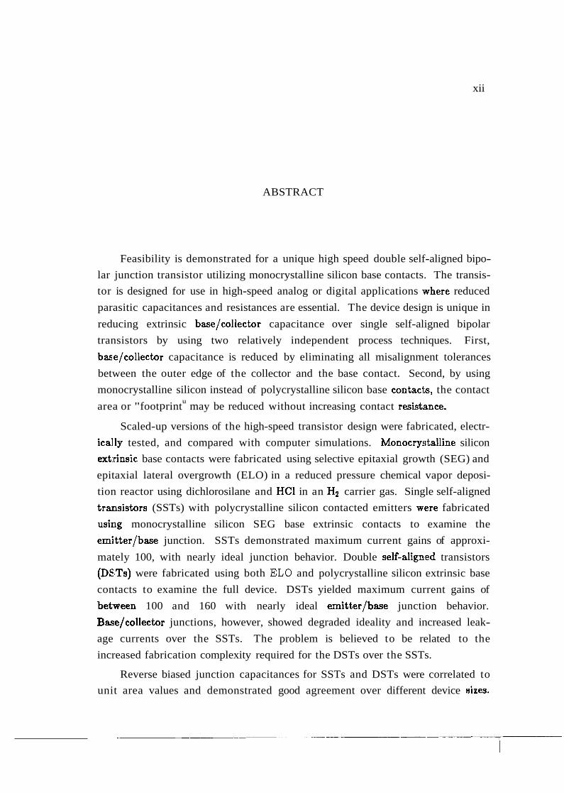
ABSTRACT
Feasibility is demonstrated for a unique high speed double self-aligned bipo-
lar junction transistor utilizing monocrystalline silicon base contacts. The transis-
tor is designed for use in high-speed analog or digital applications -where reduced
parasitic capacitances and resistances are essential. The device design is unique in
reducing extrinsic base/collector capacitance over single self-aligned bipolar
transistors by using two relatively independent process techniques. First,
bas,e/collector capacitance is reduced by eliminating all misalignment tolerances
between the outer edge of the collector and the base contact. Second, by using
monocrystalline silicon instead of polycrystalline silicon base contacl,~, the contact
area or "footprintu
may be reduced without increasing contact resist:snce.
Scaled-up versions of the high-speed transistor design were fabricated, electr-
ical.ly tested, and compared with computer simulations. Monocry~jtalline silicon
ext:rinsic base contacts were fabricated using selective epitaxial growth (SEG) and
epitaxial lateral overgrowth (ELO) in a reduced pressure chemical vapor deposi-
tion reactor using dichlorosilane and HCl in an Hz carrier gas. Single self-aligned
trrussistors (SSTs) with polycrystalline silicon contacted emitters wlere fabricated
using monocrystalline silicon SEG base extrinsic contacts to examine the
emitter/base junction. SSTs demonstrated maximum current gains of approxi-
mately 100, with nearly ideal junction behavior. Double self-align'ed transistors
(DSiTs) were fabricated using both EL0 and polycrystalline silicon extrinsic base
contacts to examine the full device. DSTs yielded maximum current gains of
between 100 and 160 with nearly ideal emitter/base junction behavior.
Base/collector junctions, however, showed degraded ideality and increased leak-
age currents over the SSTs. The problem is believed to be related to the
increased fabrication complexity required for the DSTs over the SSTs.
Reverse biased junction capacitances for SSTs and DSTs were correlated to
unit area values and demonstrated good agreement over different device sizes.
xiii
1l.esistor test structures indicate that polycrystalline silicon extrin~~ic base contacts
will have increased contact resistance over monocrystalline silicaln base contacts
by a factor of about 2. SUPREM-N and PISCES-IIB twedimensional computer
si.mulations of the fabrication process and electrical characteristics respectively
were compared against structural and electrical data to establish. a base line for
the simulation tools. Simulation tools were then used to predict the electrical
b'ehavior of the fully scaled-down version of the proposed device indicating a 45%
d.ecrease in base/collector capacitance over a comparable single elf-aligned bipe
1:nr transistor. A simulation was also performed to measure the transient response
of a 50mV applied input step to the base in a common emitter amplifier
configuration. With a 5kfl collector load, the proposed double self-aligned
transistor exhibited a 20% faster collector current response time than a compar-
a.ble single self-aligned device.
CHAPTER 1
INTRODUCTION
1.1 Research Motivation
For silicon bipolar transistors, first introduced in the mid 19,50s, significant
milestones have included the development of planar fabrication processes leading
to the integrated circuit (1960s), the development of local oxida.tion of silicon
(LOCOS) isolation techniques (1970s), and the investigation of silicon-on-insulator
(SOI) and heterojunction technologies (1960s - 1980s). Parallel research efforts
into both the bipolar junction transistor (BJT) and the metal oxide
se:miconductor (MOS) transistor have lead to multiplying ,the speed of
te(zhnologica1 advancement.
One clear example of this parallel has been the ~ompet~ition between
complementary MOS (CMOS) logic and bipolar emitter-coupled logic (ECL) for
applications in high-speed computing. Fundamentally, MOS technologies lend
well to high-speed applications which require low power, high integration densities
and require modest heat dissipation. Self-aligned gate technologies, where
channel length is determined by feature size and not misalignm.ent tolerances
between source, gate and drain, have been invaluable to achieving high
integration, high-speed CMOS with minimal parasitic delays. Despite these
attributes, bipolar ECL has remained a competitive force in applications requiring
ultra-high speed, high current drive and moderate to high integration densities.
Applications for high-speed ECL include input/output drivers, high-speed static
RiUlls and microprocessors such as the Y-MP series developed by Cray Research
foi: supercomputing [I]. New applications include the merger of bipolar ECL with
CIJIOS (BiCMOS) to gain both high-speed and reduced power consumption 121.
One reason for the continued competitiveness of high-speed bipolar
technologies, has been the advent of self-aligned fabrication schemes which lower
enlitter/base capacitance (Ceb), collector/base capacitance (Ccb), as well as
emitter (r,), base (rb), and collector resistances (r,) [3,4]. First intiroduced in the
1:xte 19709, the super self-aligned transistor (SST) format was designed to reduce
Ceb by eliminating registration misalignment tolerances between emitter and base
a s well as their contacts (31. As a windfall, the design resulted in lower Ccb, due to
reduced emitter/base area, but suffered from the continued areis dependence of
Ccb on registration tolerances between the extrinsic base and collector.
While reducing Ceb will improve intrinsic device speed, the reduction of Ccb,
zrnd therefore Miller capacitance, will be more important to improving ECL
circuit speed [5,6]. This occurs mainly because ECL is an analog circuit which is
used for digital applications. In response to this need, several "double" self-
aligned emitter/base/collector formats were developed during the late 19809,
where the minimum width of the collector/base junction could 'be reduced from
about 2pm, for a single self-aligned device, to the order of lprn [7,8]. Despite
l,hese developments, relatively little attention has been paid to double self-
alignment concepts as a means of increasing speed.
Reports have suggested that reducing intrinsic parasitics through lateral and
.vertical scale-down will ultimately be limited by the onset of phenomenon such as
high-level injection (9,101, base current reversal [11,12], and forward bias
.tunneling [13]. Unfortunately, the majority of research directed towards reducing
(extrinsic parasitics, such as r, and rbx, has centered around the use of heavily-
doped polysilicon or polysilicided extrinsic contacts. Inherent pi:oblems with the
use of polysilicon included the formation of reproducible, oxide-free
poly/substrate interfaces, the migration and segregation of dopants along grain
boundaries, and the process complexity and unreliability of poly silicidation [14].
In addition, the use of polysilicon contacts forces the use of poly-oxides or
plasma-deposited oxides for contact isolation. To date, of the limited double
self-aligned BJT designs that have been fabricated, all uti1i;ae polysilicon or
polysilicide in the extrinsic contacts.
1.2 Overview of Proposed Bipolar Transistor
Fundamental limitations to both device scale-down and poilysilicon extrinsic
contacts in bipolar transistors will force the need for design solutions which
reduce both intrinsic and extrinsic parasitics. An alternative to polysilicon
contacts would be the use of single-crystal silicon. Single-crystal contacts would
provide for lower contact sheet resistance, better contact/substrate interfaces and
higher quality oxides grown from monocrystalline silicon. The realization of
single-crystal contacts would be contingent upon meeting two requirements.
Firat, a production compatible process for manufacturing reproducible
monocrystalline silicon in self-aligned devices would be needed. Second, high-
speed self-aligned transistor applications would need to be developeld whereby the
full benefits of single-crystal silicon contacts could be exploited and tested.
To address the manufacturing of single-crystal silicon contacts, selective
epit'axial growth (SEG) and epitaxial lateral overgrowth (ELO) of silicon has been
investigated [15,16,17]. Using SEG and ELO, monocrystalline silicon can be
formed in minute geometries or grown over non-planar topologies i,o create local
SO1 regions. SEG and EL0 are attractive for advanced device applications due to
reduced growth temperatures, reduced growth pressures and the ability to use
production compatible epitaxial reactors. Under typical growth conditions, the
presence of native oxides a t the SEG and EL0 contact/substrate interface will be
com.pletely eliminated. Unlike conventional SO1 technologies, silicon is deposited
only in the desired locations and may not require lithographic definition after
growth. In this way, self-aligned contacts may be grown "as is". Finally, the use
of SEG and EL0 in advanced self-aligned devices is virtu all;^ unexplored
[18,19,20].
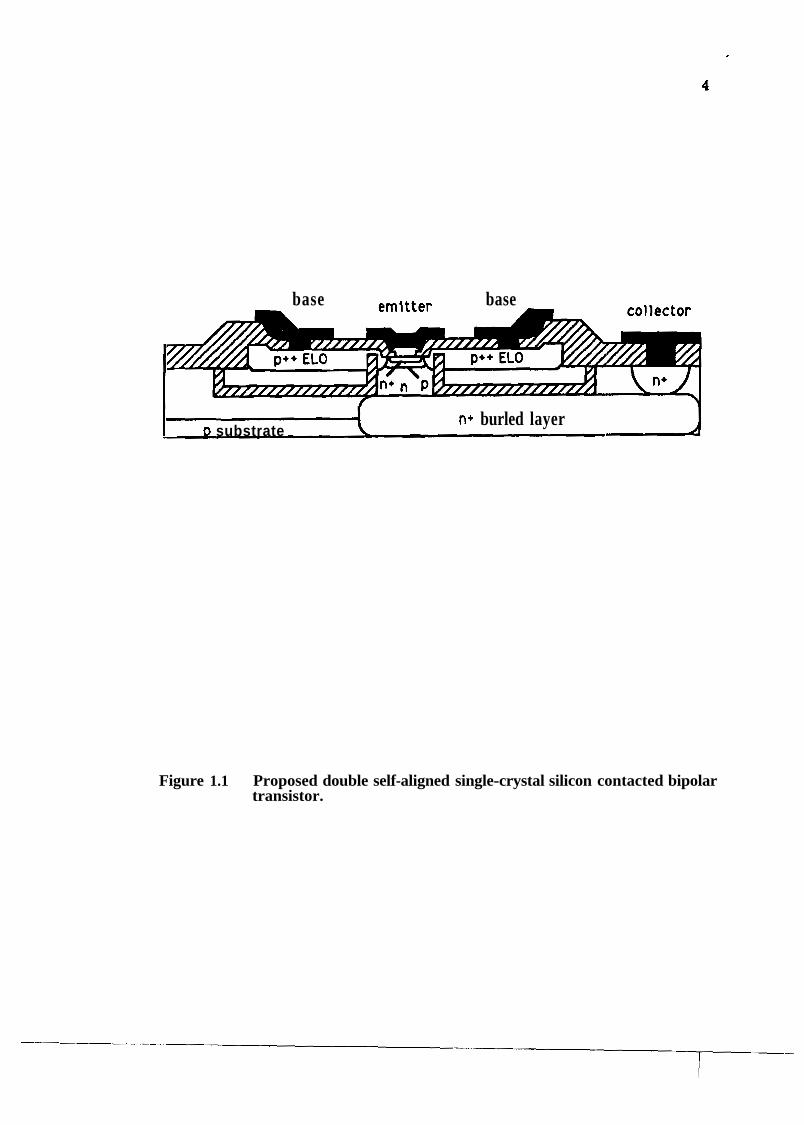
To approach the application of SEG and ELO, an advanced BlJT with self-
aligned emitter/base/collector for minimum Ceb and CCb was developed [21,22].
The final device cross-section is illustrated in Figure 1.1. The structure utilizes
single-crystal silicon extrinsic extrinsic contacts as well as oxides grown from
single-crystal silicon to reduce rbx. The extrinsic base contacts are grown using
ELC) and are inherently self-aligned to the collector pedestal. After growth, the
base! contacts are ion implanted and sidewall oxides are grovvn from the
monocrystalline EL0 silicon to self-align the emitter. The intrinsic emitter, base
and collector are fabricated in the substrate collector pedestal, therefore avoiding
any reliance on the material quality of the grown contacts for intrinsic device
performance. The extrinsic emitter contact may either be single-crystal silicon
SEG or deposit polysilicon. Using double self-alignment and self-aligned contacts,
only seven lithographic steps are required to first metal. The process uses no
critical alignment steps for fabrication of the intrinsic device.
base base
D substrate n+ burled layer J
Figure 1.1 Proposed double self-aligned single-crystal silicon contacted bipolar transistor.
1.31 Research Overview
In this report, we demonstrate the successful design, fabrication, and testing
of a DST similar to that in Figure 1.1. The fabricated device structure was
simplified in the following manner to reduce process complexity. First, a
po:llycrystalline silicon emitter was used in place of an SEG emitter. Second, the
fully single-crystal silicon E L 0 base contact was modified so that alnly the first 4
prr~ of the contact was grown from ELO. The remaining length of the contact
was fabricated from polycrystalline silicon to reduce the need for long EL0
growth times. In this way, the critical portion of the base contact directly
adjacent to the emitter was fabricated of single-crystal silicon while non-critical
tail of the contact was fabricated out of polysilicon. For comparison, DSTs were
fabricated with fully polysilicon base contacts in parallel with tqhe EL0 base
contacted DSTs. Third, a buried subcollector was replaced by the use of an n-
type substrate.
Finally, the fabrication process was not designed to yield a high-speed device
due to the rigid process controls which are required to achieve ultra-shallow
junlction depths and sub-micron lithographic feature sizes. Instead, the fabrication
sequence was designed for modest junction depths and minimum feature sizes of
2p1n to allow for easier fabrication. SSTs and substrate test devices were
fabricated to examine critical design issues separately. Resistor test structures
were fabricated to examine the difference in resistance between polycrystalline
silicon and monocrystalline silicon base contacts.
D.c. measurements of the fabricated BJTs were performed to extract forward
active and reverse breakdown characteristics. Substrate BJTs, SS'I's , and DSTs
with polycrystalline silicon emitter contacts were found to have nearly ideal
emltterlbase junctions, repeatable junction breakdown characteristics, and
for-ward current gains in the range of 100 to 170. DSTs showed degraded
coll.ector/base junction ideality of 1.25 and enhanced reverse collector/base
junction leakage currents over SSTe which was constant for different device sizes.
Por~sible reasons for the leakage include random defects caused by the LOCOS
oxidation or defects in the four outside corners of the extrinsic 'base collector
junction. A.c. characteristics for SSTs and DSTs yielded unit area base/collector
ancl baselemitter junction capacitances which were consistent over two different
device sizes.
SUPREM-IV and PISCES-IIB computer simulations showed reasonable
a.greement with measured structural and electrical data. A fully scaled-down
high-speed version of the proposed device was simulated to predict the ultimate
speed performance of this technology. For comparison, a fully scaled SST was
simulated using the same intrinsic junction depths, spacer widths, emitter area,
and collector profile as the fully scaled DST simulation. The fully scaled DST
clemonstrates about a 45% reduction in CCb over the comparable SST while
having the same hFE-max, rbx, and Ceb. Transient response time of collector
current to a 50mV input step is about 20% faster for the DST than for the SST
given a 5kR collector load. Using fabricated test structures, it was determined
t,hat monocrystalline EL0 silicon reduces extrinsic base contact, resistance over
polycrystalline by a factor of about 2 given the same contact size.
11.4 Thesis Overview
Chapter 2 will discuss previous research into SEG and EL0 technologies,
self-aligned BJT device design, and potential limitations to latc2ral and vertical
device scaledown. Chapter 3 will discuss the proposed singlecrystal silicon
contacted self-aligned BJT. Chapter 4 will discuss process development of the
fabricated BJTs and resistor test structures. Spreading resistance profiles and
scanning electron micrographs will be compared with SUPIEEM-IV process
simulations. Chapter 5 will present d.c and a.c electrical nneasurements to
compare electrical data with PISCES-rn device simu1atio:ns. Chapter 6
SUPREM-IV and PISCES-W will discuss computer simulations of the fully
scaled version of the proposed device. Chapter 7 will discuss future research.
CHAPTER 2
LITERATURE SURVEY
2.1 Scope and Purpose
The following chapter will summarize published research whicb. relates to the
pralposed single-crystal silicon contacted high-speed BJT. Topics will include a
discussion of SEG and E L 0 silicon growth technologies, an overview of
fundamental high-speed BJT operation and state-of-the-art advances and
limitations to increasing BJT speed through down-scaling intrinsic device
dimensions. The overall purpose for this review will be to outline the limitations
of current high-speed BJT designs, and to review alternative methods for
improving speed. The relevance of SEG and EL0 will be discussed.
2.2 Background: Selective Epitaxial Growth (SEG) of Silicon
2.2..1 Formats: SEG, ELO, CLSEG
The need for high-speed device performance and increased device packing
density has lead to interest in both junction and dielectric isolation techniques
[23]. Although most isolation technologies have advantages, virtually all have serious drawbacks such as non-repeatability, the use of non-production
conipatible processing equipment, unacceptable dielectric leakage, or the creation
of low material quality SO1 layers. In order to create local SO1 layers which
provide large surface area for device fabrication, a form of vapor phase chemical
vapor deposition (VPCVD) known as selective epitaxial growth (SEG) will be
examined [24].
With SEG, a continuous layer of single-crystal silicon may be deposited
adjracent to a layer of non-silicon material over a silicon substrate.
Co~lventionally, a seed hole is opened through an insulating layer, such as silicon
dioxide (Si02) or silicon nitride (Si3N4), over a single-crystal si1ic:on substrate.
The substrate is then placed in a reactor where homogeneously oriented single-
CI-ystal silicon is deposited over the exposed seed hole while deposition of
randomly oriented silicon over the insulator is suppressed..The result is selective
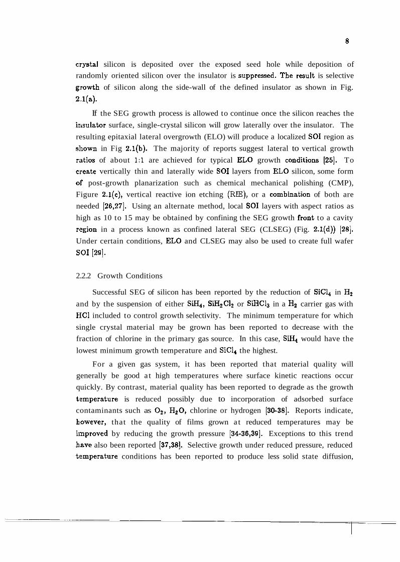
girowth of silicon along the side-wall of the defined insulator as shown in Fig.
2.3.(a).
If the SEG growth process is allowed to continue once the silicon reaches the
irlsulator surface, single-crystal silicon will grow laterally over the insulator. The
resulting epitaxial lateral overgrowth (ELO) will produce a localized SO1 region as
sllown in Fig 2.l(b). The majority of reports suggest lateral to vertical growth
ri~tios of about 1:l are achieved for typical EL0 growth condiitions [25]. To
create vertically thin and laterally wide SO1 layers from EL0 silicon, some form
OF post-growth planarization such as chemical mechanical polishing (CMP),
Figure 2.l(c), vertical reactive ion etching (RE), or a combinatiion of both are
needed [26,27]. Using an alternate method, local SO1 layers with aspect ratios as
high as 10 to 15 may be obtained by confining the SEG growth front to a cavity
region in a process known as confined lateral SEG (CLSEG) (Fig. 2.l(d)) [28].
Under certain conditions, EL0 and CLSEG may also be used to create full wafer
SO1 [29].
2.2.2 Growth Conditions
Successful SEG of silicon has been reported by the reduction of SiC14 in Hz
and by the suspension of either SNr , SN2Cl2 or SiHC13 in a H2 carrier gas with
HC1 included to control growth selectivity. The minimum temperature for which
single crystal material may be grown has been reported to decrease with the
fraction of chlorine in the primary gas source. In this case, SiH4 would have the
lowest minimum growth temperature and SiC14 the highest.
For a given gas system, it has been reported that material quality will
generally be good a t high temperatures where surface kinetic reactions occur
quickly. By contrast, material quality has been reported to degrade as the growth
tlemperature is reduced possibly due to incorporation of adsorbed surface
contaminants such as 02, HzO, chlorine or hydrogen [30-381. Reports indicate,
however, that the quality of films grown a t reduced temperatures may be
iinproved by reducing the growth pressure [34-36,391. Exceptions to this trend
have also been reported [37,38]. Selective growth under reduced pressure, reduced
tmemperature conditions has been reported to produce less solid state diffusion,
SEG -
(b) 1 substrate I I ~ l a n a r l z a t l o n etch s t o ~ I ~ l a n a r l z e d EL0
, CLSEG cavl t y support CLSEG
(d) 1 substrate _I
Figure 2.1 Cross-sectional drawings showing, (a) selective epitaxial growth (SEG), (b) epitaxial lateral overgrowth (ELO), (c) plmarized ELO, and (d) confined lateral SEG (CLSEG).
better pattern transfer, and, in some cases, less auto-doping [24,35,40].
For advanced device applications, the choice of a gas systern will therefore
constitute a series of tradeoffs involving parameters such as growth selectivity, gas
purity, production compatibility, pressure range, and temperature range. To
grow device-quality material at reduced temperatures, much of the research as
been focused on the use of S'iH2C12, dichlorosilane (DCS), as a primary gas source
fbr reduced-pressure, reduced-temperature selective epitaxy. Among other
attributes, DCS is reported to show improved stability, safety and cleanliness over
SiH4, reduced growth temperature requirements over SiC14, and ease of use over
SiHC13. Numerous reports have been published detailing the affect of DCS-based
growth conditions on seed hole precleaning, growth selectivity, material quality,
imd Si02 degradation [16,24,25,34,39,41-431. In addition, the influence of growth
conditions on selective doping by introduction of n-type or p type gasses into the
gas stream is significant [44]. This subsection will highlight the most important
effects and will summarize the influence of reactor geometry on growth conditions.
!2.2.2.1 Preclean
In order for high quality crystalline silicon to be grown using SEG, native
oxides must be removed from the SEG seed holes prior to growth. Conditions
.necessary for the removal or growth of Si02 on silicon substrates under high
vacuum conditions, lo-' to lo-' Torr, have been published by Ghidini and Smith
132,331. They report that for clean (100) silicon surfaces, a set of criteria on
temperature and partial pressure of O2 and H 2 0 exist to remove oxides from the
silicon surface through
Si + SiOz <==> LSiO(v) (2.1)
where SiO(v) represents the volatile product of oxide etching. In separate studies,
the removal of native oxides or intentional passivation layers prior to selective
growth has been reported for reduced temperatures using ultira high vacuum
(UHV) conditions [35,45,46].
In reduced pressure CVD processes, the removal of native oxides prior to
growth is usually accomplished by introducing Hz into the reactor ambient for
several minutes a t temperatures between 850 and 1100 ' C and pressures between
25 and 760 Torr [16-18,24,25,41-43,471. The cleaning procesrs may begin a t
pinhole sites in the native oxide where a source of both silicon, from the
substrate, and Si02 are present a t the surface. Reports indicate that the native
oxide removal process can result in field oxide degradation. Studies indicate that
even high-quality MOS gate oxides may be damaged by the reactor ambient
during prebake under certain conditions [43]. The incident of oxidle failure was
reported to be more severe for thinner oxides.
In an attempt to predict oxide degradation during preclean, Friedrich et a1
[361 have extrapolated the data obtained by Ghidini and S:mith to the
temperature and pressure range of interest in RPCVD processes. 'The resulting
criteria, shown in Figure 2.2 (taken from [36]), are reported to provide a general
guideline for performing H2 precleaning in a regime where field or gate oxide
degradation is minimized while allowing for complete native oxide removal. In
contrast, recent reports [37,38] suggests that the minimum temperature and
pressure criteria outlined by Ghidini and Smith for moisture contarnination may
be overly stringent for VPCVD performed a t atmospheric pressure. To minimize
dopant redistribution in advanced structures, the lowest possible preclean
temperature must be utilized. More research on this topic appears to be
necessary.
2.2,.2.2 Material Quality
After precleaning of SEG seed holes, an HCl etch may be performed to etch
silicon in the seed hole. Following the etch step, DCS gas is added to induce
selective epitaxy. Reports indicate that epitaxial growth carried out over
incompletely cleaned seed holes will result in poor film quality [4'7]. Similarly,
epitaxial growth which is carried out in a contaminated reactor ambient, may
result in poor material quality due to the incorporation of contamiinants in the
growing film. Initial studies into reduced temperature epitaxy were based upon
the notion that a reduction in pressure would lead to a reductio~l in required
growth temperature. One explanation for this phenomenon was that lower
pre:ssures would remove adsorbed surface species such as H* or ~f which were
thought to block the migration of growth species [30].
Alternatively, it has been hypothesized that moisture contami~lation in the
reactor might be an overriding factor in determining the material quality of
silicon grown under reduced temperatures [35-381. In the case wherle moisture is
the main reactor contaminant, the guidelines given in Figure 2.2, for seed hole
Moisture Content [ppm] -
Figure 2.2 Diagram, taken from reference 361, which displays critical moisture, pressure and temperature con itions for successful SEG preclean and growth.
6
preclean, may also represent critical conditions for oxide removal during SEG film
growth [36]. Furthermore, it has been reported that the additioln of a silicon
containing gas species into the reactor ambient, such as DCS, will accelerate the
degradation of thin field oxides beyond that observed during H2 preclean [43].
Otlher reports also indicate that field oxide thinning may occur as a result of E L 0
film growth [48]. A tradeoff therefore exists between having enough moisture to
prevent excessive field oxide degradation and not having so much that
incorporation of moisture into the SEG film will degrade material quality.
To evaluate material quality, reports comparing the performance of bipolar
and MOS devices fabricated in SEG and EL0 versus ones fabricated in substrate
silicon may be divided into those which address *'bulk" SEG material quality and
those which address SEG sidewall defects. Diodes and BJTs fabricated in large
area SEG silicon (away from SEG sidewalls), are reported to show diode ideality,
leakage currents, minority carrier lifetimes and transistor current gains
conlparable to those found in bulk devices (491. The same study indicates that
growth interruption, followed by external processing and reincorporation into the
reactor for further SEG will produce device quality material a3 well. MOS
devices fabricated in selectively grown silicon have also been reported [15-
18,:25,50].
Numerous studies have also been reported concerning the effect on material
qua.lity of SEG growth along oxide sidewalls (see reference (51) for a list). These
studies indicate that seed hole orientation will affect material qualit:y through the
formation of defects a t or near the SEG/sidewall interface. Minimizing of defect
formation during epitaxy has been experimentally reported for (100) oriented
wafers when seed holes are aligned along <loo> directions. Reguardless of
orientation, however, published studies indicate that pn junction diodes which
intersect any SEG growth sidewall will suffer at least an order of magnitude
increase in reverse bias leakage currents as well as reduced breakclown voltages
over identical planar bulk diodes [18,51].
Finally, it has been reported that selectively n-type doped SEG films may be
grown a t relatively low temperatures (900 ' C) and pressures (70 Torr) by
introducing pH3 into the DCS, Hz, HCl gas stream [44]. P-type dolping has also
been reported under reduced temperature and pressure conditio:ns [20]. The
inhence of high dopant levels within the crystal lattice or through surface
kinetics may cause material quality to degrade over undoped f i lms . In general,
higher growth temperatures seem to allow for higher average dopant
inlcorporation and better material quality. For applications in advanced devices,
low temperature processing may force design tradeoffs in this area.
2.2.2.3 Selectivity
In addition to material quality, growth selectivity is an important factor in
determining process parameters. Ideally, one would like to grow SEG and EL0 layers from defined seed holes only. Unfortunately, random polysillicon nucleation
on field oxides and nitrides (non-selective growth) has been widely reported. Both
Claassen and Bloem 1521 as well as Yew and Reif 1531 have reported that, under
selective CVD growth conditions, a critical amount of time is needed before
polysilicon nucleates can form over field oxides. Using a SiH4-based, low
temperature, single wafer reactor, Yew and Reif [54] have capitalized on this
delay time by developing a plasma etch process whereby argon ions are used to
clean field nucleates before they can form critical clusters. While the argon
plasma will etch some of the intended SEG material as well, the SEG film will be
able to achieve a net positive growth rate as the nucleates are removed before
t!hey may contaminate the field.
More conventionally, Claassen and Bloem 131) reported a theory for
atmospheric pressure, low temperature (T < 1000 ' C) molecular growth kinetics
using DCS, Hz, and HCl which may provide insight into reduced pressure growth
selectivity. The major process steps are given below.
(a) After the supply of DCS is moved to the substrate surface through mass
transport, gas phase reactions converted the DCS into energetically
favorable gas species,
s ~ H ~ c ~ ~ <==> Sic12 (g) +Hz (2.2)
(b) The most energetically favorable gas species near the substrate is adsorb
onto the substrate surface as a mobile species,
(c) Surface reactions occur where mobile adsorbed species arrive at kink sites
or surface steps and incorporate into the silicon film,
SiClz(st) +Hz (g) <==> Si(cr) + 2HCI(g)
where (2.7) is assumed to be the growth rate limiting reaction at reduced
temperatures due to reduced energy for surface kinetics. The overall DCS growth
reaction will give off HCI as a by-product,
SiHz C12 (b) <==> Si(cr) + 2HCl(g)
In this formula set, (g) denotes a gas, (*) denotes a free surface site on the
substrate, (s*) denotes an adsorbed surface species, (st) denotes a species at a
surface step site, and (cr) denotes a crystal lattice site.
According to this model, the DCS, Hz, HCI gas system will produce HCl both
by the net growth reaction (2.8) and by the addition of HCl dlirectly to the
reactor ambient. The resulting HCl concentration will serve to etch silicon at
surface steps, possibly via the reverse of processes in equations (2.6) and (2.7).
Since the DCS concentration will control not only silicon growth, but the
pralduction of some HCl as well, the relation between DCS and added HCl gas
con.centrations will be a complex function of reactor geometry, temperature and
pressure. Assuming that a delay time occurs before polysilicon nucleates can form
over the field oxide [52,53], selectivity will be achieved when the total DCS/HCl
gas ratio, reactor pressure, and reactor temperature are tailored to allow for both
etching of field nucleates and a positive SEG growth rate. The i~ltroduction of
HCl gas may, however, degrade material quality due to the existence of metallic
con taminants.
2.2-2.4 Reactor Geometry
Finally, a large body of data exists to define the gas flow dynamics involved
within different reactor designs. Of interest here, is the work :performed on
pancake-type cold wall reactors which utilize a rotating S ic coated. susceptor, as
in the Solid State facility a t Purdue [24,40,41,47,55,56]. The most serious
problems to be addressed by these studies include growth rate u~iiformity across
the susceptor, growth rate uniformity across each wafer, and absollute growth rate
as a function of gas composition, temperature and pressure. The general trends
suggest that better growth rate uniformity across each wafer and from wafer to wafer may be achieved by lowering the growth pressure, increming the growth
r,ate, and increasing the fraction of open silicon area to field oxilde area on each
wafer. Growth rate uniformities as low as 1% have been reported for pancake
t~ype reactors [57]. A more complete explanation of geometry effects may be
albtained elsewhere (471.
11.2.3 Applications
To end the section on selective growth processes, we give two distinct
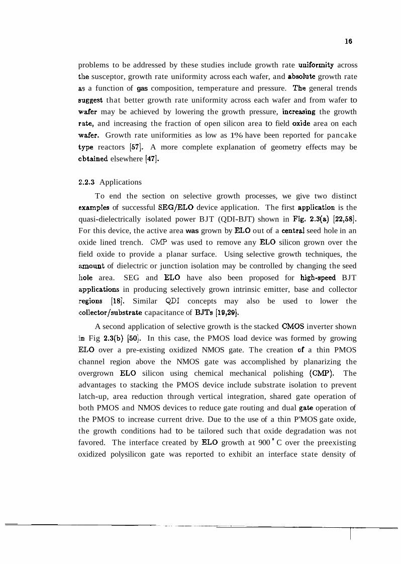
examples of successful SEG/ELO device application. The first a:pplication is the
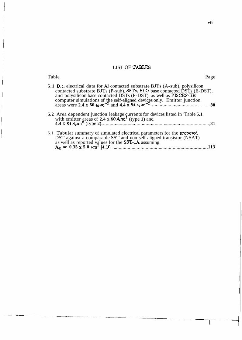
quasi-dielectrically isolated power BJT (QDI-BJT) shown in Fig;. 2.3(a) [22,58].
For this device, the active area was grown by EL0 out of a centra.1 seed hole in an
oxide lined trench. CMP was used to remove any EL0 silicon grown over the
field oxide to provide a planar surface. Using selective growth techniques, the
itmount of dielectric or junction isolation may be controlled by changing the seed
hole area. SEG and EL0 have also been proposed for :high-speed BJT
:spplications in producing selectively grown intrinsic emitter, base and collector
regions [IS]. Similar QDI concepts may also be used to lower the
collector/substrate capacitance of BJTs [19,29].
A second application of selective growth is the stacked CMOS inverter shown
iin Fig 2.3(b) [50]. In this case, the PMOS load device was formed by growing
:EL0 over a pre-existing oxidized NMOS gate. The creation of a thin PMOS
channel region above the NMOS gate was accomplished by planarizing the
overgrown EL0 silicon using chemical mechanical polishing (CMP). The
advantages to stacking the PMOS device include substrate isolation to prevent
latch-up, area reduction through vertical integration, shared gate operation of
both PMOS and NMOS devices to reduce gate routing and dual gate operation of
the PMOS to increase current drive. Due to the use of a thin P'MOS gate oxide,
the growth conditions had to be tailored such that oxide degradation was not
favored. The interface created by E L 0 growth a t 900 C over the preexisting
oxidized polysilicon gate was reported to exhibit an interface state density of
collector base emltter collector
I substrate I
[a) UDD OUT
I p-type substrate I
Figure 2.3 Cross-sectional drawings of (a) the quasi-dielectrically isolated BJT and (b) the bdimensional CMOS inverter fabricated by SEG and EL0 [SO].
2:~10"cm-~ a t mid-gap [IS]. The above results illustrate the usefulness of SEG
and E L 0 for fabrication of advanced structures.
2.3 High-Speed BJTs (I): Design Considerations
The switching response of a bipolar transistor is limited both by the intrinsic
delay of the transistor itself, and by the parasitic effect of other circuit elements
on the transistor. In reality, these two delay groups may not be decoupled due to iinteractions between extrinsic and intrinsic components. It is instructive to
analyze delay components separately, however, to investigate design tradeoffi. In the following sections, the intrinsic propagation delay of an unloaded bipolar
transistor under low and high level injection conditions is examined. The effects
of circuit delay on the switching speed of ECL digital logic circu.its will then be
cliscussed to outline areas where delay may be reduced. ECL was chosen for
situdy over -other bipolar logic circuits such as I ~ L or TTL due to superior
frequency response and wide application in high-speed computing. For clarity,
+,he discussion will be limited to room temperature operation ad homojunction
devices.
:2.3.1 Transistor delay
Intrinsic propagation delay through the bipolar transistor may be analyzed
'by several methods including charge control concepts, equivalent circuit models or
computer algorithms [60]. For large signal transients where the transistor may be
switching through different regions of operation, such as from cutoff to saturation,
most of the delay will be incurred when changing operation regions due to the
rearrangement of large amounts of charge. For non-saturating digital logic, such
as ECL or current-mode logic (CML), the transistors are switched by small signal
transients and remain within the active region a t all times. For these cases, the
intrinsic switching response is effectively modeled by assuming isolated
propagation delay terms for the emitter, base, and collector.
2.3.1.1 Propagation Delay Model
To model the propagation delay of carriers through an isolated bipolar
transistor, the transit delay through the emitter/base junction, qnasi-neutral base,
base/collector junction, and base/collector deletion region, as :shown in Figure
2.4, is examined. For this analysis, the transistor is characterizetl by two RC
delays, an emitter charging time (7,) and a collector charging time (T,)), and two
transit delays, an intrinsic base transit time (rb) and a base/collector depletion
region transit time (7,) [61,62]. The expressions for each delay telrm are given
below
Wcb 7, = -
2vd
Folr these expressions, Ceb and Ccb are the emitterlbase and collector/base
capacitances, re and rc are the small signal emitter and collector resistances, v
represents the base charge profile ( v rrr 2 for uniform base doping under low-level
injection), Db is the base minority carrier diffusion coefficient, vd is the electron
drift velocity, and pc is the collector resistivity. The geometric parameters are
defined in Figure 2.4.
The summation of these four transit delays may be related to the transit
frelquency fT, the frequency a t which the unloaded transistor exhibits unity
forward current gain ,8, by
By examining the delay components, it is seen that maximum fT will be achieved
by reducing Ceb, Ccb, the quasi-neutral base (xl) and collector (x4-xg) widths and
p,, while increasing I, and v. Modern BJT fabrication methods have addressed
the: reduction of lateral and vertical dimensions to reduce capacitancte and transit
distances, especially within the quasi-neutral base [3]. In addition, v can be
increased substantially by grading the base dopant profile [60]. Hawever, design
tradeoffs place limitations to speed improvement. For example, reduction of base
wiclth, to reduce r b , must be accompanied by an increase in base doping to
prevent base-width modulation [63] or an increase in base resistance. An increase
in base doping will lower forward current gain and increase the emitterlbase
emitter/base base/collector buried c:ollector
r 'i"ctiOn f junction junction
I I I space-charge I -
h I I - - - region . . . . . . . .
I ; 1 - . . . . . . . . .
I . . . . , . . 1 I 1
collector
. . . . . . X
4 x (depth)
Figure 2.4 Diagram showing the pro agation delay through a BJT by (a) diagram of transistor and (by schematic definition of delay terms.
capacitance which will increase re. Alternatively, T, may be reduced by shrinking
the! base/collector space-charge width Wcb but will result in larger Ccb and an
increased re and T,,. Numerous other tradeoffs exist as well.
2.3.1.2 High-Level Injection Effects
The propagation delay model presented in the previous section was derived
under the assumption of low level injection. As device dimensions are continually
scaled down to improve switching speed, the ability to scale power rgupply voltage
ant1 biasing current may be limited by circuit requirements. As a result, the
current densities within modern high-speed BJTs have continually increased to
the point where high-level injection within the collector may occur a t collector
currents which are within the range of digital circuit applications (0.1 - 1.0 mA).
To model the effects of high-level injection on fT, the prop:sgation delay
expression must be modified.
To illustrate the problem, a plot showing the variation of fT with collector
current I, is given in Figure 2.5. Relating to the Figure, it is observed that the
intirinsic frequency response is poor a t low I, due to large re (2.9). As I, increases,
the value of fT increases with decreasing re until a peak is reached (fTm,) a t a
current I,,,. As I, is increased further, the frequency response degrades due to
increased rb. Other time constants will contribute to the overall shape of the fT
curve but will generally be less significant.
Two major theories have been proposed to explain the high-current roll-off of
fT [62,65]. The most widely accepted explanation is that high-level injection
within the base/collector space-charge region (SCR) causes the quasi-neutral base
wid.th to expand and therefore increase rb . This phenomenon, known as the base
push-out effect or "Kirk effect", occurs when the density of free charge entering
the collector SCR becomes comparable to the background impurity charge
density N,. To visualize the impact of high current densities on device operation,
one may think of superimposing a uniform sheet of negative charge over the
eollector/base SCR [66]. Within the base SCR, the added negative charge will
addl to the negative ion core density causing an effective increase in ])-type dopant
density. Within the collector SCR, the added negative charge will :subtract from
the positive ion core density causing an effective decrease in n-type dopant
density. As a result, the modified charge configuration withing the base/collector
Figure 2.5 Schematic representation of the variation of transit frequency fT with collector current &.
SClFt will have the effect of reducing the base side depletion width :and increasing
the collector side depletion width. With a reduced base depletion width, the
effective quasi-neutral base width will be increased resulting in a larger rb.
To quantify this condition, the Poisson equation governing the n-type
collector SCR can be modified to include a term representing the free electron
drift current [62,65] (Jc/vdq)
As the drift charge density becomes comparable to the background doping
density within the collector SCR, the increase in r b will cause fT to roll off at a
curl-ent in the range of [60]
If tlie collector current is continually increased, high-level injection will reportedly
force the quasi-neutral base to extend into the collector region effectively widening
the base further. Under this condition, r b will increase substantially and the total
base resistance rb will decrease. At very high collector current densities, high-
level injection within the base will induce conductivity modulation ('Nebster effect
(671). A more complete description of other high-level injection phenomenon is given elsewhere [65].
For high-speed BJT designs, the parameter Jo may be considered a rough
indicator for the onset of high-level injection. A more detailed expression for Jo
would include the effects of Vcb and epitaxial layer thickness [65]. To first order,
one would design a high-speed transistor to have a Jo which is above the intended
current density to be used for circuit applications. For most transistor designs, J,
mayp be increased by increasing N,. As a tradeoff, raising Nc will rc~sult in lower
collector/base breakdown voltages and increased Ccb. Another drawback to
increasing Nc is the onset of base current reversal [11,12]. In this case, as N, is
incrleased, the average electric field ECb will also increase for a fixed Vcb. The
resulting increase in avalancheinduced electrons and holes will cause large
amounts of hole current to drift into the intrinsic base from the collector/base
SCEt. For sufficient Nc values, avalancheinduced hole currents miiy become as
large or larger than the base terminal current causing the terminal current to
decrease or reverse in sign. High-level injection and base current reversal may
therefore represent lower and upper boundary conditions irespectively for
dletermining the value of N,.
2.3.2 Circuit Delay
The critical parameters which influence circuit speed are now examined. As
an overview, the effects of Miller capacitance on analog and digital circuits using
the hybrid-7r model are first examined. Next, a theoretical propagation delay
e:npression for ECL circuits is discussed to extract the most significant parasitic
components.
2.3.2.1 Hybrid-7r Circuit Model
The propagation delay model discussed in section 2.3.1 gives excellent
physical insight into fT, but fails to examine the effects of circuit feedback on
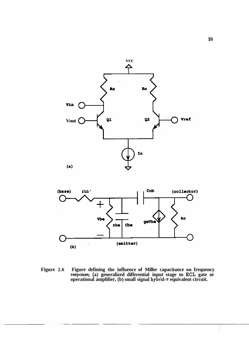
small signal frequency response. To examine the influence of parasitic circuit
delay, the differential transistor pair shown in Figure 2.6(a) is analysed. For
practical purposes, this circuit could represent a portion of the differential input
to either an ECL logic gate or an analog operational amplifier. In either case,
small signal behavior may be modeled in the active region by the hybrid-7r
equivalent circuit shown in Figure 2.6(b).
In the simplest case, the hybrid-7r model can be used to estimate fT by
temporarily shorting out the collector resistance R,. Assuming low-level
injection, the result will be a single pole frequency response
14s with the propagation delay expression of section 2.3.1, the ,fT measurement
only reflects intrinsic device speed. In addition, the open loop voltage gain is
shorted out during an fT measurement [68].
With R, at the collector node in figure 2.6, the common emitter open loop
voltage gain is
The effect of this voltage gain will be to place an added effective capacitance on
top of the base/collector feedback capacitance Ccb. In essence, the added voltage
vcc
Via
Vout
Ib8ra) rbb ' (col1ac:tor)
(emittar) 'd
Figure 2.6 Figure defining the influence of Miller capacitance on frequency
response; I a) generalized differential input stage to ECL gate or operationa amplifier, (b) small signal hybrid-.rr equivalent circuit.
drop from input to output forces added current to be drawn in charging and
discharging Ccb. The added current draw makes Ccb look; like a larger
capacitance than for the short circuit fT case. The effective Ccb or Miller
capacitance CM will be proportional to the voltage gain by
For analog circuit applications, a large voltage gain will be essential for
:amplification of small signals. The price for this voltage gain will be a large Miller
(capacitance which will magnify any Ccb related RC time const;mts resulting in
:poor frequency response. A typical analog amplifier may utilize an Rc of 5 kn. By
contrast, high-speed digital circuits, such as ECL, require small voltage gain and
minimum CM. For ECL applications, R, may be in the range of 1.0 k n or less.
2.3.2.2 ECL Circuit Delay Expression
To approach the specific delay components which influeince ECL circuit
speed, the single-stage inverter shown in Figure 2.7(a) .is examined. Starting with
the input voltage to Q1 at logic low, the reference transistor Q2 will be turned on
with a reference current I,. When an input step is applied to ($1, the reference
current switches from Q2 to Q1 and the output of Q1 drops to th.e logic low state.
As the output of Q1 is pulled low, the emitter follower Q3 bufft:rs the output of
Q1 to the next ECL gate. To achieve rapid switching response, the circuit must
have a fixed supply of switching current (I,), a small voltage swing (V,), and must
be designed to keep all transistors within the active region.
Several reports have been published which attempt to define the critical
parameters influencing the frequency response of high-speed ECL, circuits [5,6,69].
While it has been reported that no closed form expression may be derived to fully
model ECL gate delay [5], Stork (5,641 has published a simplified expression which
appears to accurately predict the ring oscillator speed of experimentally reported
devices. For this model, the drive transistor Q1 is subdivided into two delay
components which represent the response of collector current (Tb) and the
collector load (T,) to an input transient. A third delay term, due to the emitter
follower, is ignored (51. The combination of Tb and T, is reported to yield an
accurate first-order figure of merit for gate delay (T,)
Finally, other parameters have been reported to influence EC:L gate delay.
Most reports identify fT, Ccb, rb, and collector loading conditions 2 s critical areas
for reduction [5,6,69,71]. However, current crowding as well as re and r, may also
degrade performance under certain conditions [6,71,72]. For very small device
geometries, values of re above 1000 are reported to dramatically increase ECL
circuit delay [72]. For larger values of re, the ECL circuit may fail to switch
properly [6,72], presumably due to an excessive voltage drop across the emitter.
Intermixed with these parameters are other circuit issues such as noise margin,
voltage swing, and circuit configuration. At present, minimum gate delays for
high-speed ECL circuits have been reported within the current range of 0.1 - 5mA
[7,:10,73-761. For high integration applications, however, the power-delay product
may ultimately become limited by heat dissipation requirements which may
restrict driving currents to the range of 0.1 mA.
2.4 High-Speed BJTs (11): Design Implementations
2.4.1 Perspective on LOCOS Isolation
The propagation delay expressions derived in the previous seetions indicate
thart maximizing the speed of bipolar transistors and ECL logic circuits will
involve numerous design tradeoffs. To minimize gate delay one should design for
minimum Ccb, rb, re, Ces and extrinsic load resistances while designing for
maximum fT [5,6,69,71,72]. In itself, fT will be maximized when intrinsic
capacitances as well as re and r, are reduced and the base region is optimized for
impurity profile and carrier transit time. Limitations to geometric scale down
include high-level injection effects within the collector, base-width modulation,
and collector/base avalanching effects. [6,11-13,62,65,72]. At the same time,
circuit reliability and power requirements may place additional constraints on
operating conditions.
To implement these design criteria, there has been a steady trend towards
fabricating device geometries which reduce lateral area cape~citances and
resistances as well as reduce intrinsic transit distances through base and collector.
The driving force in this reguard as been the development of self-alignment
scbemes which eliminate the need for the registration misalignment tolerances of
conventional LOCOS isolation. Figure 2.8(a) shows the amount of lateral area
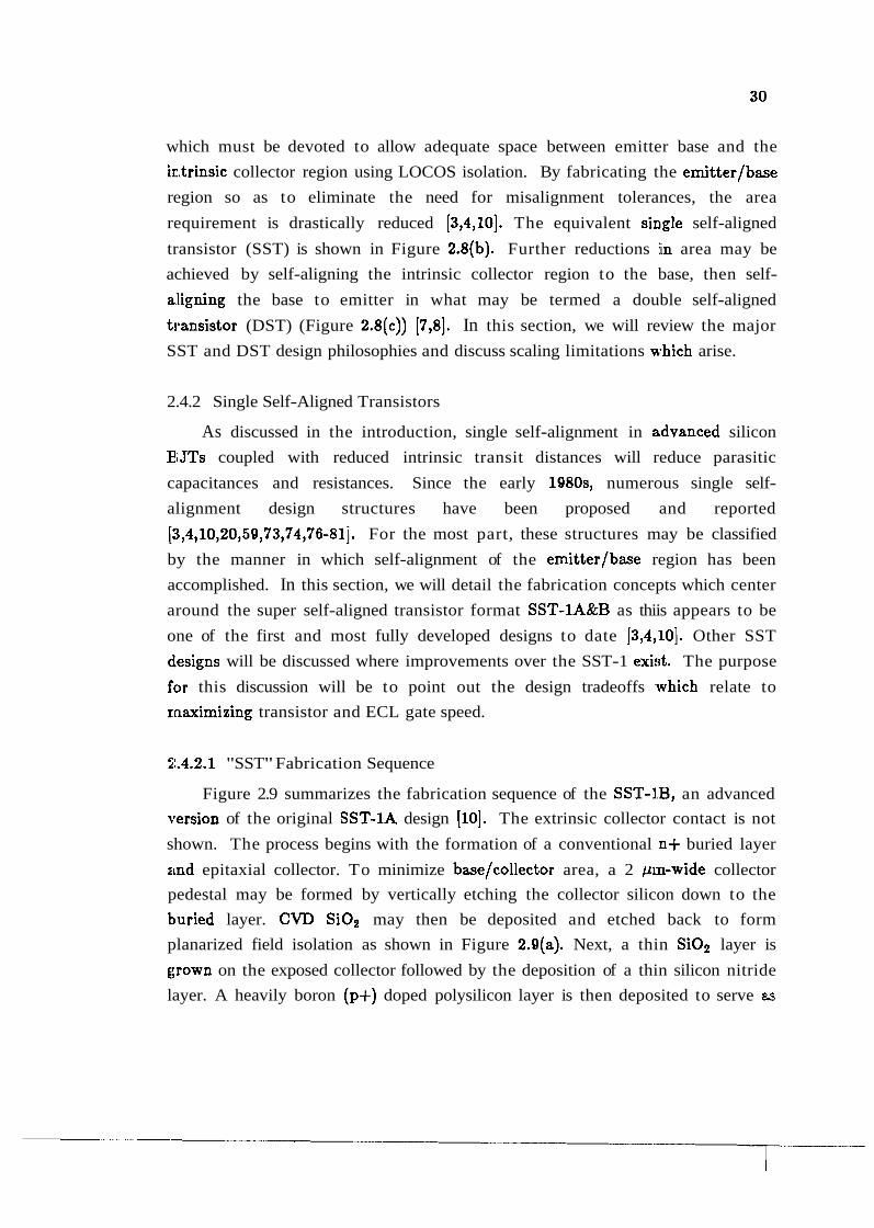
which must be devoted to allow adequate space between emitter base and the
intrinsic collector region using LOCOS isolation. By fabricating the emitter/base
region so as to eliminate the need for misalignment tolerances, the area
requirement is drastically reduced [3,4,10]. The equivalent single self-aligned
transistor (SST) is shown in Figure 2.8(b). Further reductions iin area may be
achieved by self-aligning the intrinsic collector region to the base, then self-
aligning the base to emitter in what may be termed a double self-aligned
transistor (DST) (Figure 2.8(c)) [7,8]. In this section, we will review the major
SST and DST design philosophies and discuss scaling limitations which arise.
2.4.2 Single Self-Aligned Transistors
As discussed in the introduction, single self-alignment in a.dvanced silicon
BJTs coupled with reduced intrinsic transit distances will reduce parasitic
capacitances and resistances. Since the early 1980s, numerous single self-
alignment design structures have been proposed and reported
[:3,4,10,20,59,73,74,76-811. For the most part, these structures may be classified
by the manner in which self-alignment of the emitter/base region has been
accomplished. In this section, we will detail the fabrication concepts which center
around the super self-aligned transistor format SST-1A&B as thiis appears to be
one of the first and most fully developed designs to date [3,4,10]. Other SST
d.esigns will be discussed where improvements over the SST-1 exist. The purpose
f'or this discussion will be to point out the design tradeoffs .which relate to
maximizing transistor and ECL gate speed.
21.4.2.1 "SST" Fabrication Sequence
Figure 2.9 summarizes the fabrication sequence of the SST-1.B, an advanced
version of the original SST-1A design (101. The extrinsic collector contact is not
shown. The process begins with the formation of a conventional n+ buried layer
zmd epitaxial collector. To minimize base/collector area, a 2 pm-wide collector
pedestal may be formed by vertically etching the collector silicon down to the
buried layer. CVD Si02 may then be deposited and etched back to form
planarized field isolation as shown in Figure 2.9(a). Next, a thin SiOt layer is
grown on the exposed collector followed by the deposition of a thin silicon nitride
layer. A heavily boron (p+) doped polysilicon layer is then deposited to serve as
base emltter base
Figure 2.8 Diagram, from 7 , showing the scaling differencme between (a) LOCOS isolation BJ T, (b) SST, and (c) DST.
(dl n+ poly slllcon spacer
(el
base emltter base
Figure 2.9 SST process sequence 1101 showing (a) ~ollect~or pedestal, (b) alignment of base contacts with pedestal, (c) undercutting base contacts, (d) link-up of base contacts, (e) self-aligned emitter cavity, and (f) final structure.
the extrinsic base contact. Polysilicon outside of the transistor active area is
selectively oxidized. At this point, the foundation for a self-aligned emitter/base
region is created by vertically etching a 0.8 to 1.0 pm wide hole in the polysilicon
layer down to the nitride. The exposed polysilicon is subsequently oxidized to
forrn an isolation layer while the nitride blocks oxidation of the collector pedestal
(Figure 2.9(b)). The exposed nitride layer is now etched until a sufficient amount
of undercutting beneath the polysilicon is achieved. The newly exposed stress
relief oxide is subsequently etched to expose the collector pedestal as shown in
Figure 2.9(c).
At this point, heavily p-type doped polysilicon is deposited to fill the space
between the overhanging polysilicon layer and the collector pedest:al. Unwanted
polysilicon is removed by vertical reactive ion etching and the exposed polysilicon
under the polysilicon base contacts is oxidized. During oxidation, the heavily
doped p-type polysilicon over the collector pedestal serves as a diffusion source to
dope the extrinsic base link-up region as shown in Figure 2.9(d). The intrinsic
base region is now ion implanted using the the extrinsic base colntacts as an
implant mask. Concurrently, a deep n-type collector implant is :performed to
selelctively raise the collector doping level right below the intrinsic base region.
Following these implantations, heavily arsenic-doped (n+) ]?olysilicon is
. deptosited and reactively ion etching down to the intrinsic base silicon. A self-
aligned cavity for the emitter is formed in this way due to the existence of the
neair vertical sidewalls on the extrinsic base contacts as shown in Figure 2.9(e).
Fin;~lly, the emitter and extrinsic collector contact are fabricated by depositing
and defining heavily arsenic-doped polysilicon. The complete struciture, without
collector contact or trench isolation, is shown in Figure 2.9(f). As shown, the
extrinsic base contact is isolated from the emitter contact by poly-oxides
sidewalls. At the same time, a polysilicon sidewall spacer, formed by the first
emitter polysilicon deposition, keeps the emitter impurity profile from intersecting
the diffused portion of the extrinsic base contact. For the completed structure,
the emitter is 0.35pm wide and the collector pedestal is approxin~ately 2.0pm
wide.
2.4.2.2 Design Tradeoffs
Evaluation of the fabrication sequence reveals that this structure has several
advantages over conventional LOCOS BJTs. First, the lateral width of the
emitter has been reduced to less than a feature size and has been symmetrically
placed into the center of the intrinsic base region by self-alignment. By itself, a
narrow emitter geometry will result in reduced Ceb and intrinsic rb. As a
vrindfall, the entire device footprint will be reduced resulting in lower Ccb and
C,,, due to the elimination of misalignment tolerances between Ithe emitter and
extrinsic base. To gain even more speed, the intrinsic transit distances are
normally reduced, especially within the base, necessitating an increase in base
doping density to keep rb from increasing. The combination of narrow geometry
and heavily doped extrinsic contacts will allow for high fT, as well as low Ccb,
C,,, and rb.
A series of design tradeoffs may influence the use of emitterlbase sidewall
spacers [82]. Higher fT will be achieved when junction capacitances are reduced.
For this reason, the diffused extrinsic base region should be kept lto within 100 to
300nm of the emitter by tailoring the sidewall oxide spacer length. The penalty
for significant overlap of the emitter and extrinsic base dopant profiles will be
lower reverse bias emitterlbase breakdown voltages and increased base
~eecombination. While transistors which are used in ECL circuits are not
subjected to emitterlbase reverse bias, n+/p+ diodes demonstrake forward bias
tunneling which may set limits to the amount of encrouchment possible [13].
Once the emitter width, sidewall oxide spacer, and extrinsic base contact
footprint have been established, the vertical dopant profile for emitter, base, and
collector must be designed. In particular, as device dimensions shrink, the
increase in collector current density will cause the premature onset of high-level
injection within the collector/base space charge region [62,65]. Tlie resulting base
push-out effect will necessitate an increase in collector doping (N,) to prevent fT
~:oll-off. In the SST-lB, this problem has been addressed by adding a selectively
implanted collector (SIC) during intrinsic base formation as shown in Figure
:2.9(e). The resulting local increase in collector doping just beneath the intrinsic
lbase has been reported to hold off the point to which base push-out will occur
.without increasing the entire intrinsic collector doping level. Other researchers
!have had success in limiting base push-out by grading the collector impurity

profile between the buried layer to the collector/base junction.
While raising Nc will help lower series resistance and reduce base push-out,
the result will be increased electric fields within the collector/base SCR which will
1ow.er the collector/base breakdown voltage or cause base current reversal [11,12].
Reports indicate that base current reversal may be eliminated by beaving a low-
doped intrinsic layer (i-layer) in between the intrinsic base and the otherwise
molderately doped collector [12]. An example of doping levels flor an i-layer
configuration would be N ~ N I . ( ) x ~ o ~ ~ c ~ - ~ , N~ ~ 5 . 0 ~ 1 0 ~ ~ c m - ~ , and
N, rz3.0x10"cm-~ (121. Experimentally, the introduction of an i-1a.yer has been
replorted to reduce fT and Ccb while increasing collector/base breakdown voltage
over an identical transistor with no i-layer [83]. Using the i-layer concept, the
reduction in Ccb may prove more advantageous for improving ECL circuit delay
than the small reduction in fT (831.
2.4.2.3 Related Structures
We now investigate alternative single self-aligned design concepts which
difizr from the SST. For the most part, non-SST designs tend to resemble the
SST upon completion but follow different paths getting there. One method has
beein to replace the extrinsic base contact poly-oxide sidewall spacer with
deposited borosilicate glass [74]. The glass is reported to serves as both a good
isolation layer as well as a source of out-diffused boron in forming the extrinsic to
intrinsic base link-up region. Other researchers have investigated alternative
sidewall spacers such as dual oxide-nitride layers (841. One set of processes, which
incc~rporates well into BiCMOS application, involves creating single self-aligned
BJll's in a similar manner as self-aligned MOS gates [85,86]. In these cases, the
emitter is defined first, followed by the formation of an emitter sidewall spacer.
Self-aligned extrinsic base contact regions are then formed around the emitter by
depositing doped polysilicon or by ion implantation.
As a separate category, selective epitaxial growth has also been reported for
high-speed BJT applications. In these cases, SEG has been utiliaed to grow
selectively-doped epitaxial base regions in an effort to obtain well defined and
shallow base doping profiles [59,79]. EL0 has also been reported in some cases to form part of the extrinsic base contact (791. All structures of this type, which
have been manufactured, have been SSTs with most or all of the extrinsic base
contact being doped polysilicon. Other SST structures have bee:n proposed and
dlemonstrate theoretical potential for high-speed application (191. In all cases,
these structures suggest the possibility for incorporating SEG and E L 0 into
a.dvanced bipolar structures to improve parasitic capacitance and resistance.
Research into selective epitaxial growth for novel high-speed device applications
asppears to be a relatively unexplored field.
21.4.3 Double Self-Aligned Transistors
As discussed in the previous section, emitter/base self-alignment will reduced
parasitic capacitances and base resistance. A common drawback in all of these
processes, however, is the failure to utilize a self-alignment procless to align the
extrinsic base with the collector pedestal. As shown in Figure 2.9, any portion of
the diffused extrinsic base within the collector pedestal which doer not connect to
the intrinsic base will contribute nothing but parasitic base/collector capacitance.
I3y using a process which, in a single step, aligns the extrinsic base to the collector
pedestal and subsequently allows for alignment of the emitter to the base, the
parasitic extrinsic base can be almost completely eliminated. This will translate
directly into reducing extrinsic collector/base junction area and collector pedestal
width therefore reducing extrinsic collector/base capacitance (Ccbx) and C,.
f!.4.3.1 "J3AS1Cw Fabrication Sequence
In general, DSTs are designed as sidewall contacted type structures (SICOS)
but need not be as a rule [7,8,75]. Very few reports concerning vertically base
c:ontacted DSTs appear to exist [75]. As an example of a SICOS DST, a process
c:alled "BASIC" is reviewed and the potential advantages over SS'l's are explained
[8]. The BASIC process starts with a conventional n+ buried layer and epitaxial c:ollector. Over the epitaxial collector, a stress relief oxide is grown followed by
t.he deposition of a thin silicon nitride layer. On top of the nitride, a polysilicon
plug is then formed by deposition and reactive ion etching.. The plug is
s'ubsequently oxidized while the nitride blocks oxidation of the sublstrate as shown
in Figure 2.10(a). With this configuration, the oxidized polysilico~l plug serves as
zcn ideal mask for selective vertical etching of the epitaxial silicon to form the
c:ollector pedestal (Figure 2.10(b)).
poly s l l lyn SIOZ d
n* buried layer P-
n* burled layer
(c)
p** polysilicon
I n+ buried layer ID'-
n* burled layer I I _ I
n++ poly tlllcoa
I n* burled layer ITI
Figure 2.10 Double self-aligned "EiASIC" fabrication sequence [8] showing formation of (a) polysilicon plug, (b) self-aligned collector pedestal, (c) base contact isolation, (d) sidewall extrinsic base contacts, (e) extrinsic base link-up region, and (f) final structure.
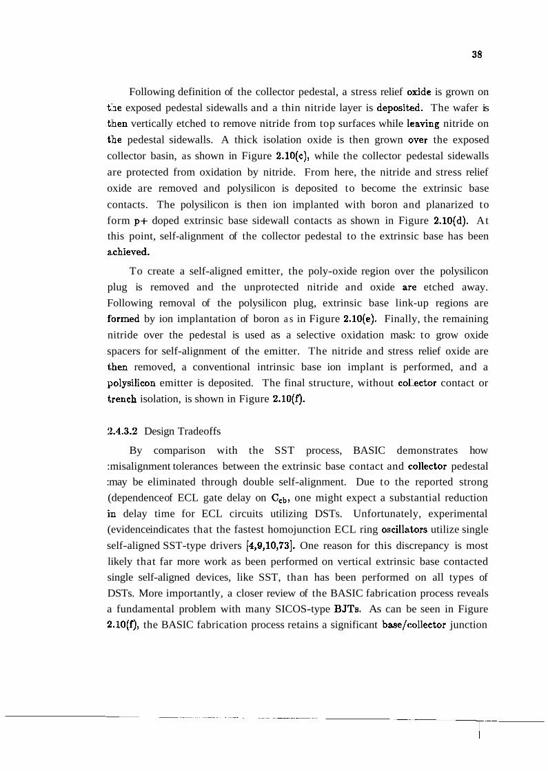
Following definition of the collector pedestal, a stress relief oxide is grown on
tlne exposed pedestal sidewalls and a thin nitride layer is depositeld. The wafer is
then vertically etched to remove nitride from top surfaces while 1e.aving nitride on
the pedestal sidewalls. A thick isolation oxide is then grown over the exposed
collector basin, as shown in Figure 2.10(c), while the collector pedestal sidewalls
are protected from oxidation by nitride. From here, the nitride and stress relief
oxide are removed and polysilicon is deposited to become the extrinsic base
contacts. The polysilicon is then ion implanted with boron and planarized to
form p+ doped extrinsic base sidewall contacts as shown in Figure 2.10(d). At
this point, self-alignment of the collector pedestal to the extrinsic base has been
a.chieved.
To create a self-aligned emitter, the poly-oxide region over the polysilicon
plug is removed and the unprotected nitride and oxide arc etched away.
Following removal of the polysilicon plug, extrinsic base link-up regions are
formed by ion implantation of boron a s in Figure 2.10(e). Finally, the remaining
nitride over the pedestal is used as a selective oxidation mask: to grow oxide
spacers for self-alignment of the emitter. The nitride and stress relief oxide are
then removed, a conventional intrinsic base ion implant is performed, and a
~~olysilicon emitter is deposited. The final structure, without colllector contact or
trench isolation, is shown in Figure 2.10(f).
2.4.3.2 Design Tradeoffs
By comparison with the SST process, BASIC demonstrates how
:misalignment tolerances between the extrinsic base contact and c:ollector pedestal
:may be eliminated through double self-alignment. Due to the reported strong
(dependence of ECL gate delay on Ccb, one might expect a substantial reduction
iin delay time for ECL circuits utilizing DSTs. Unfortunately, experimental
(evidence indicates that the fastest homojunction ECL ring oscilla.tors utilize single
self-aligned SST-type drivers [4,9,10,73]. One reason for this discrepancy is most
likely that far more work as been performed on vertical extrinsic base contacted
single self-aligned devices, like SST, than has been performed on all types of
DSTs. More importantly, a closer review of the BASIC fabrication process reveals
a fundamental problem with many SICOS-type BJTs. As can be seen in Figure
2.10(f), the BASIC fabrication process retains a significant base/collector junction
perimeter along the collector pedestal sidewall. Therefore, while the SICOS
format will allow for reduced collector pedestal area, the total extrinsic
co:llector/base capacitance, and therefore ECL gate delay, may not be
significantly reduced.
There appears to be no published reports of double self-aligned designs which
utilize fully vertical extrinsic base contacts. In one case, a design was found
which utilizes a combination of vertical and sidewall extrinsic base contacting ['I].
For this structure, the contact cross-section between the extrinsic polysilicon
electrodes and the single-crystal silicon was reduced to 0.25pm in o.rder to reduce
the collector pedestal area. Unfortunately, the device exhibited poor ECL ring
osciillator speed due to large base resistance, which was attributed to the extrinsic
base polysilicon electrodes and the poly/single-crystal contact resistance. For
fu tilre high-speed ECL, DSTs will need to have reduced collector/base
capacitance without increased extrinsic resistance.
2.4.4 Heterojunction Bipolar Transistors
2.4.4.1 Overview
We conclude the section on transistor designs with a review of heterojunction
BJTs (HBTs). In general, two types of HBTs have relevance to high-speed silicon
device applications, wide band-gap amorphous silicon [87,88] or SiC [89] emitter
transistors and narrow band-gap SiGe base [20,64,83,90,91] devices.
Fun.damentally, both types of HBT operate on the principle that band offsets
between the emitter and base will provide enhanced forward current gain. In this
case!, a band line-up which causes the valence band edge of the emitter to have a
lower energy than that of the base will establish a potential step and cause the
baclc injection of minority carriers from base to emitter to decrease. At the same
time, one would like the conduction band line-up to produce a favorable
contlition for the forward flow of carriers from emitter to base. Assuming this is
achieved, the emitter injection efficiency (7) will increase resulting in large current
gain..
The increased 7 will also allow for base doping to be increased and emitter
doping to be decreased without substantial loss of current gain. Heavy base
doping will allow fT to be increased by reducing the quasi-neutral base width
without increasing base width modulation or base resistance. Indi:rectly, a heavily
doped base will also allow the collector doping to be increased to reduce high-level
injection. A lower emitter doping coupled with a moderately high base doping
will also result in lower emitterlbase capacitance as well. Finally, low
temperature operation of homojunction devices will most often result in reduced
y, and therefore lower current gain, due to band-gap narrowing; in the emitter
(021. By contrast, the combination of band offset between emitter and base
cloupled with lower emitter doping will allow HBTs to operate at very low
temperatures without substantial loss of y.
2.4.4.2 Wide Band-Gap Emitters
Reports detailing the experimental operation of HBTs using either
a,morphous-Si or S ic wide-gap emitters or SiGe narrow-gap bases suggest
clisadvantages to HBT device processing. For wide-gap emitters, amorphous
silicon offers low process complexity a t low deposition temjperatures. Post
processing after deposition must be restricted to low temperatures however, to prevent conversion of amorphous to poly-crystalline material. Conversely, both
single-crystal as well as poly-crystal S ic emitters have been reported (891. The
growth temperature of single-crystal Sic, about 1000 ' C, make:s the use of this
inaterial less attractive for high-speed device dopant profiles. Stoichiometric
poly-crystalline S ic emitters are reported to have comparable band-gaps to
:stoichiometric single-crystal S ic (2.2 - 2.3eV), deliver high current gains, and can
'be grown with moderate doping densities a t 900 ' C.
12.4.4.3 Narrow Band-Gap Bases
More recently, a large amount of research has been performed on strained
layer Si/SiGe/Si emitter/base/collector heterostructures for EET applications
[20,64,83,90,91.]. In all cases, post-growth processing must be kept to reduced
temperatures, to avoid layer damage. By tailoring the Ge fraction, the SiGe layer
non-strained band-gap and strain-influenced band-gap will be determined. In a
related way, SiGe layers with useful Ge fractions are reportedly restricted to less
than lOOnm in order to avoid destructive strain relief [93],, Typically, the
increased base doping level and desire for reduced base transit time will
ultimately limit quasi-neutral base thickness.
To date, SiGe base HBTs post the fastest fT of any silicon bipolar technology
[83]. An increase in ECL circuit speed has also been reported over comparable
hoinojunction devices [83]. However, these devices were not self-aligned and the
operating current for maximum fT was quite high. Some progress has been
reported on producing single self-aligned SiGe HJ3Ts but no reports appear to
exist for DST devices. From a practicality standpoint, it is unclear what the long
term effects of operational environment will be on the SiGe strained layer,
especially thermal cycling during low temperature use. HBTs in general should
also be constrained by the same limitations placed on homojt~nction BJTs.
Fin.ally, the concepts used to describe transit times through the base will need to
be revised when the quasi-neutral base width is reduced to a level where ballistic
transport may occur.
2.4.5 Scaling Limitations to Polysilicon Technologies
A review of the designs presented in this section suggests that scaling of
intirinsic and extrinsic dimensions to reduce parasitic delays has been
accomplished through the exclusive use of polysilicon-based technologies.
Theoretically, polysilicon serves to reduce the slope of the minority carrier
diffusion profile within the emitter resulting in a higher current gain [94]. In practice, polysilicon can be conformally deposited a t relatively low temperatures,
can be easily etched by a range of processes, may be heavily doped in-situ, and is
well understood. On the down side, native oxides a t the polysilicon,lsingle-crystal
silicon interface cause processing complexity to increase and reliability to decrease
1141.
The majority of reports concerning advanced BJTs indicate that the
po1:ysilicon base and emitter electrodes must have sufficient area to contact the
underlying single-crystal silicon in order to keep extrinsic contact rlesistance to a
mirimum. For the majority of designs, such as the SST [4,10], the cross-sectional
length of the polysilicon/single-crystal silicon contact is in the range of 0.25pm to
O.S!ipm. Attempts to reduce the cross-sectional length of the contact in order to
reduce area-dependent capacitances would increase the extrinsic resistance. While
the series resistance of polysilicon can be improved by silica ti on^, self-aligned
silicides increase processing complexity and have not been widely reported for
high-speed bipolar applications [9,14]. In order to scale down current self-aligned
designs, extrinsic contacts will either have to be fabricated using self-aligned
silicided polysilicon or the contacts will have to be fabricated out of a low
resistance alternative such as single-crystal silicon.
2..5 Chapter Summary
In summary, SEG and EL0 growth techniques have been reviewed in the
context of device applications. SEG and EL0 show promise for use in advanced
devices due to reduced temperature precleaning and growth conditions. The
ability to grow and planarize large single-crystal silicon layers over insulator has
been reported to provide enormous advantages for device integration, device
isolation, and novel device structures.
Concurrently, the evolution of high-speed BJT technology rvas reviewed as
well as the design tradeoffs which drive it. For high-speed ECL ring oscillators,
the parameters which have been reported to influence gate de1:ay are fT, base
resistance, collector/base and collector/substrate capacitances ancl circuit loading
conditions. Technologically, single self-alignment of emitter to base, combined
with vertical scaling, has been reported to increase fT and ECL switching speed
by reducing base resistance and parasitic capacitances. Double self-alignment of
emitter to base and base to collector pedestal promises to reduce gate delay
further by eliminating all intrinsic registration misalignment.
From the standpoint of applied SEG, there appears to be a need for
investigation of alternative methods for improving device speed once polysilicon
scaling limitations are reached. To this end, the use of SEG and EL0 has yet to
be experimentally reported for fully single-crystal silicon high-speed BJTs. There
rclso appear to be few reports of double self-aligned BJTs in anything other than a
SICOS-type format. A direct comparison of otherwise identical double and single
self-aligned BJTs in a vertically contacted extrinsic base format (non-SICOS) is
:LISO lacking. To date, however, the fastest devices reported have been single self-
aligned transistors. Given that the double self-aligned structurca have received
comparatively less attention, the investigation of vertically co~ltacted DSTs is
important.
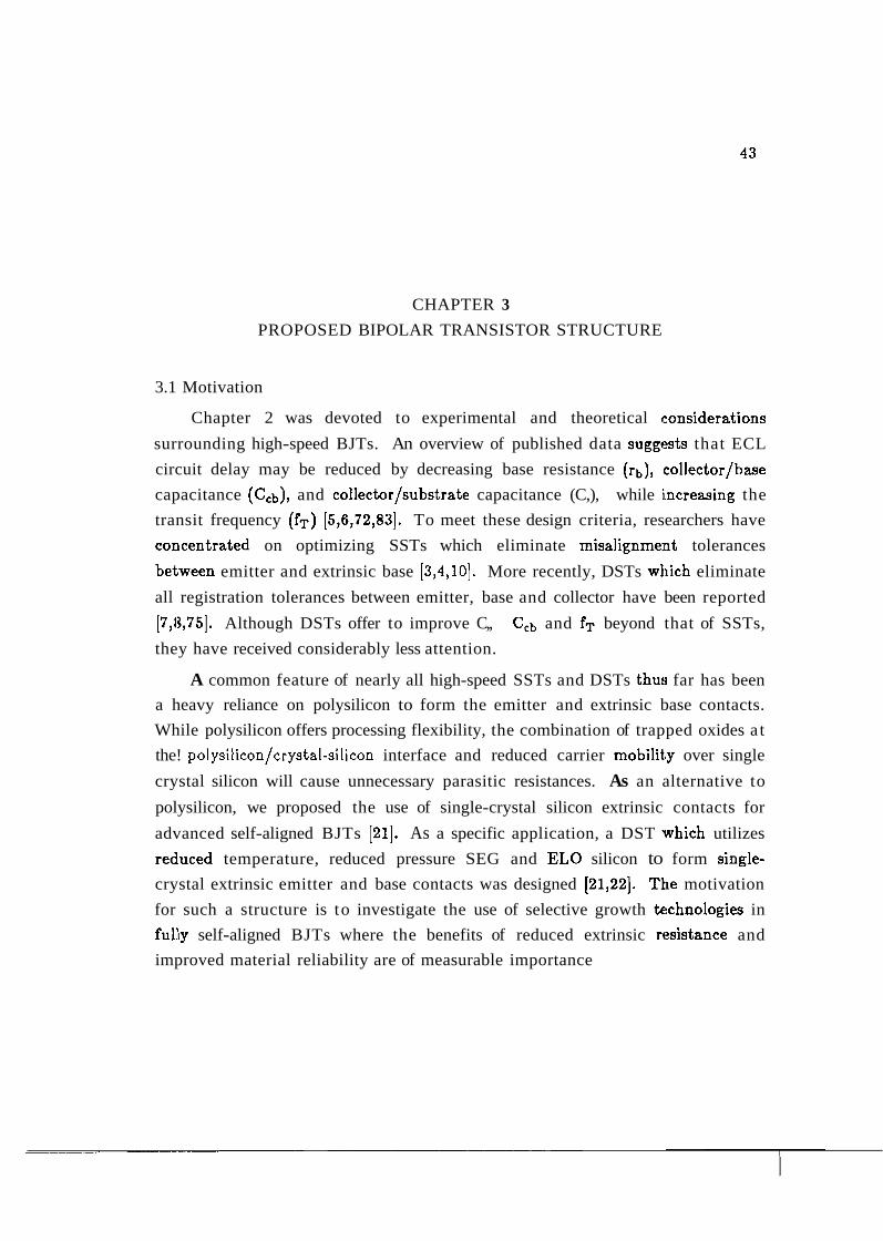
CHAPTER 3
PROPOSED BIPOLAR TRANSISTOR STRUCTURE
3.1 Motivation
Chapter 2 was devoted to experimental and theoretical r:onsiderations
surrounding high-speed BJTs. An overview of published data suggests that ECL
circuit delay may be reduced by decreasing base resistance (rb), collector/base
capacitance (Ccb), and collector/substrate capacitance (C,), while increasing the
transit frequency (fT) [5,6,72,83]. To meet these design criteria, researchers have
coricentrated on optimizing SSTs which eliminate misa1ignme:nt tolerances
between emitter and extrinsic base [3,4,10]. More recently, DSTs which eliminate
all registration tolerances between emitter, base and collector have been reported
[7,13,75]. Although DSTs offer to improve C,, CCb and fT beyond that of SSTs,
they have received considerably less attention.
A common feature of nearly all high-speed SSTs and DSTs thuca far has been
a heavy reliance on polysilicon to form the emitter and extrinsic base contacts.
While polysilicon offers processing flexibility, the combination of trapped oxides a t
the! polysilicon/crystal-silicon interface and reduced carrier mobilit,y over single
crystal silicon will cause unnecessary parasitic resistances. As an alternative to
polysilicon, we proposed the use of single-crystal silicon extrinsic contacts for
advanced self-aligned BJTs [21]. As a specific application, a DST -which utilizes
redaced temperature, reduced pressure SEG and E L 0 silicon to form single-
crystal extrinsic emitter and base contacts was designed [21,22]. The motivation
for such a structure is to investigate the use of selective growth k:chnologies in
ful.ly self-aligned BJTs where the benefits of reduced extrinsic resistance and
improved material reliability are of measurable importance
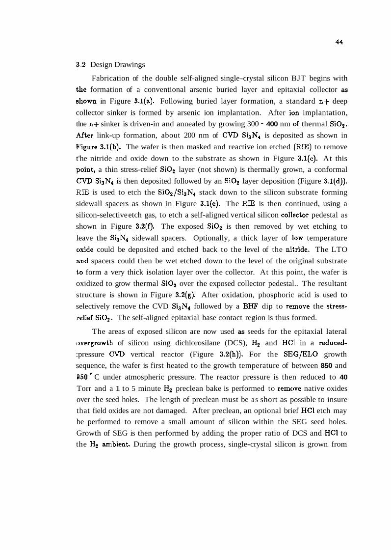
3..2 Design Drawings
Fabrication of the double self-aligned single-crystal silicon BJT begins with
the formation of a conventional arsenic buried layer and epitaxial collector as
sllown in Figure 3.l(a). Following buried layer formation, a standard n+ deep
collector sinker is formed by arsenic ion implantation. After ion implantation,
tlne n+ sinker is driven-in and annealed by growing 300 - 400 nm olf thermal .SiOz.
After link-up formation, about 200 nm of CVD Si3N4 is deposited as shown in
Figure 3.l(b). The wafer is then masked and reactive ion etched (RIE) to remove
t'he nitride and oxide down to the substrate as shown in Figure 3.l(c). At this
point, a thin stress-relief Si02 layer (not shown) is thermally grown, a conformal
C:VD Si3N4 is then deposited followed by an SiOz layer deposition (Figure 3.l(d)).
FLIE is used to etch the Si02/Si3N4 stack down to the silicon substrate forming
sidewall spacers as shown in Figure 3.l(e). The RIE is then continued, using a
silicon-selective etch gas, to etch a self-aligned vertical silicon collector pedestal as
shown in Figure 3.2(f). The exposed Si02 is then removed by wet etching to
leave the Si3N4 sidewall spacers. Optionally, a thick layer of Low temperature
oxide could be deposited and etched back to the level of the nit,ride. The LTO
:md spacers could then be wet etched down to the level of the original substrate
too form a very thick isolation layer over the collector. At this point, the wafer is
oxidized to grow thermal SiOr over the exposed collector pedestal.. The resultant
structure is shown in Figure 3.2(g). After oxidation, phosphoric acid is used to
selectively remove the CVD Si3N4 followed by a BHF dip to remove the stress-
relief SiOz. The self-aligned epitaxial base contact region is thus formed.
The areas of exposed silicon are now used as seeds for the epitaxial lateral
overgrowth of silicon using dichlorosilane (DCS), H2 and HCl in a reduced-
:pressure CVD vertical reactor (Figure 3.2(h)). For the SEG/ELO growth
sequence, the wafer is first heated to the growth temperature of between 850 and
050 C under atmospheric pressure. The reactor pressure is then reduced to 40
Torr and a 1 to 5 minute Hz preclean bake is performed to remove native oxides
over the seed holes. The length of preclean must be a s short as possible to insure
that field oxides are not damaged. After preclean, an optional brief HC1 etch may
be performed to remove a small amount of silicon within the SEG seed holes.
Growth of SEG is then performed by adding the proper ratio of DCS and HCl to
the H2 ambient. During the growth process, single-crystal silicon is grown from
n eptaxial col lector 3
D S w t t n+ burled layer 4
(a)
oxlde/nitrlde spacer
Figure 3.1 Cross sections of the proposed BJT showing buried layer and epitaxial collector, deep collector link-up, RIES, (d) sidewall spacer deposition, (e) spacer RIE.
p substrate n* burled layer
te)
E L 0 slngle-crystal SlllCOn
/ Dlanarlzed E L 0 slllcon .
I p Substrate n* burled layer
(h)
:Figure 3.2 Cross sectionsc of the proposed BJT showing (f) collector pedestal RE, (g) LOCOS, (h) ELO, and (i) CMP.
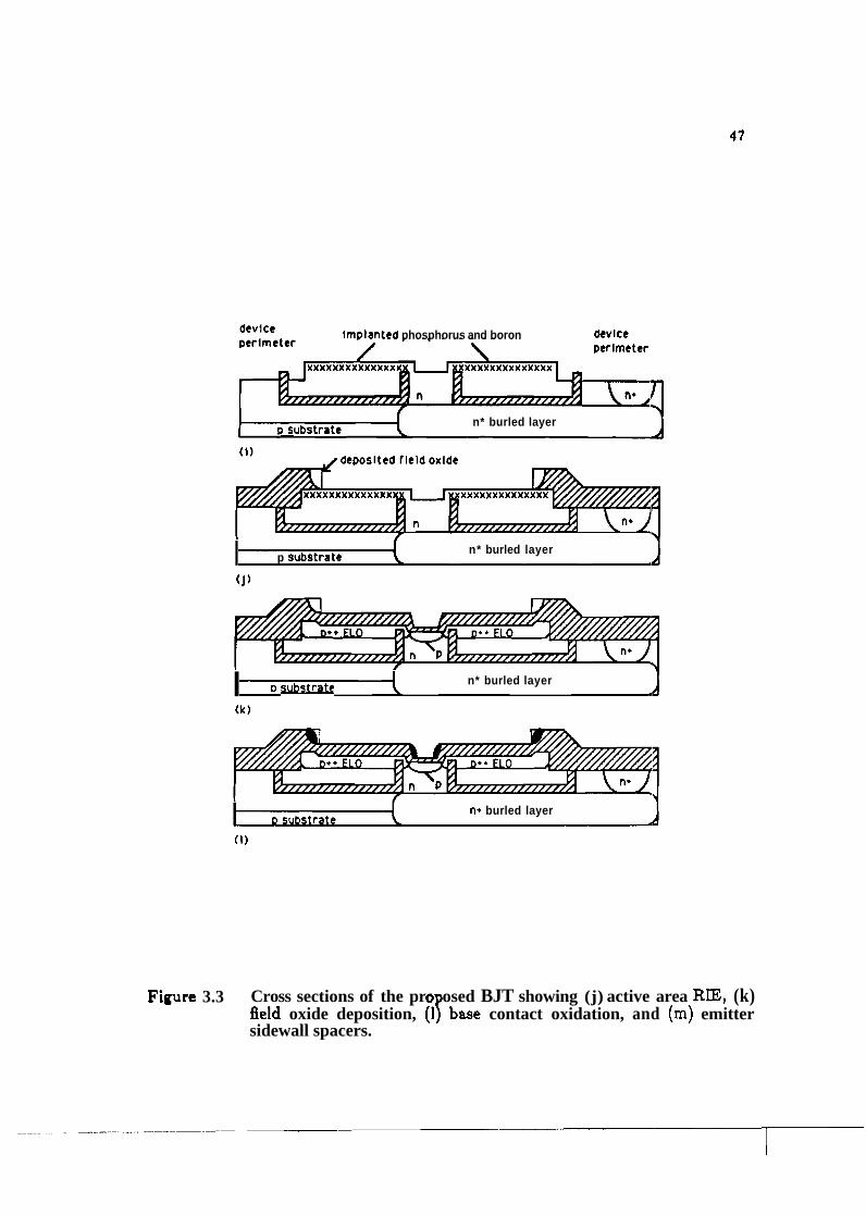
devlce implanted phosphorus and boron
n* burled layer p substrate
I n* burled layer p substrate
(1)
I n* burled layer D w r a t e
(k)
I n+ burled layer D s ~ p ~ t r a t e
( 1 )
Figure 3.3 Cross sections of the pro osed BJT showing (j) active area RE, (k) field oxide deposition, (I! b w contact oxidation, and (m) emitter sidewall spacers.
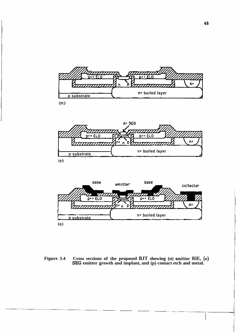
I n+ burled layer p substrate
(m)
I n+ burled layer p substrate
(n)
n+ burled layer D substrate
( 0 )
Figure 3.4 Cross sections of the proposed BJT showing (n) emitter RIE, (0)
SEG emitter growth and implant, and (p) contact etch and metal.
adjacent seed holes over the pedestal isolation regions and field Si02. The
adjacent growth fronts should merge together over the SiOz to create a continuos
layer of E L 0 silicon. Chemical mechanical polishing (CMP) is now used to
reduce the vertical level of silicon to the thermal Si02 etch stop giving the profile
shown in Figure 3.2(i).
The crucial process steps to achieving self-alignment of the emitter are now
undertaken by ion-implanting the exposed base contact regions with a heavy dose
of boron. For this step, the Si02 etch stop also serves as an imp1an.t mask. After
im]>lantation, all of the exposed Si02 is removed by selective wet etching. An
active area mask is now used to define and vertically etch the external boundaries
of the E L 0 base contacts. As a result of etching, the E L 0 base contacts are
electrically disconnected from the secondary E L 0 seed holes a t the perimeter of
the active area as shown in Figure 3.3(j). To form field isolation, plasma Si02 is
sutlsequently deposited and etched to expose the active area (Figure 3.3 (k)).
The wafer is now oxidized a t 900' C in wet O2 to produce approximately
200 nm of oxide in the emitter trench and on the base contact sidewalls. Due to
the presence of boron impurities at the surface of the ELO-grown base contact, a
thicker oxide will be grown on the surface of the base contact than is grown in
the emitter trench [3,97] (Figure 3.3(1)). The low resistance p-type base contact
ancl base link-up regions are formed during the oxidation process as the heavy
dosage of implanted boron diffuses through the EL0 silicon. As an alternative,
one may add a small dosage of implanted phosphorus to the surface of the base
contacts during the initial boron implant. A sufficient dosage of pb.osphorus will
boost the impurity-enhanced oxide growth rate over boron alone. At the same
time, the phosphorus dosage must be low enough to be electrically compensated
by the implanted boron.
Following base contact formation, the intrinsic base is created by ion
implanting boron through the thermally-grown SiOz layer in the emitter trench.
A thin layer of either polysilicon or silicon nitride is then deposited and R E is
weld to form emitter sidewall spacers as shown in Figure 3.3(m). The emitter
trench is then opened using oxide-selective R E and the sidewall spacers are
removed (Figure 3.4(n)). After R E , the emitter cavity is implantedl with arsenic
to form the intrinsic emitter. An un-doped SEG emitter contact is subsequently
grawn then ion implanted as shown in Figure 3 4 0 ) . Alternativcely, the SEG

eniitter could be grown n-type. The full structure may then be rapidly annealed
a t high temperatures to fully activate the impurities. Finally contact holes for
the base and collector are opened and the device is metallized. The completed
st~ructure, without trench isolation, utilizes seven lithography steps and is shown
in Figure 3.4(p).
3.:3 Discussion
3.3.1 Scaling of Single-Crystal Silicon Contacts
The design presented in section 3.2 utilizes singlecrystal silicon extrinsic
crnitter and base contacts. By contrast, stateof-theart single and double self-
aligned transistors utilize polysilicon extrinsic contacts due to the ease of
processing and enhanced current gain of poly emitters over single-crystal emitters.
The use of polysilicon places limitations, however, to the integrat,ion density of
the advanced self-aligned BJTs due to contact resistance at the polg/singlecrystal
interface and metal/poly contact resistance. From an ECL circuit standpoint, it
would be desirable to minimize collector pedestal width to reduce Ccb without
increasing base or emitter resistance. At the same time, high-level injection base
push-out will place limits to the scale-down of emitter area.
Figure 3.5 shows a detailed comparison between the single self-aligned SST-
1.13 and the proposed single-crystal silicon contacted DST. For this comparison,
the differences between extrinsic base contacts will be examined by assuming that
both devices have an emitter width of 0.35 pm, an oxide spacer width of 0.26 pm,
aind an identical emitter area. The assumption of identical emitte:r area will also
create identical conditions for base push-out between the two designs. For both
d'evices, the intrinsic and extrinsic Ccb will be determined by the area of the
collector/base junction as well as the collector and base dloping profiles.
Assuming a collector/base junction depth of 0.20 pm for the SST-1B [4,10], the
total collector/base junction perimeter length may be estimated by adding the
junction length under the emitter (0.35 pm), sidewall spacers (2 x 0.26 pm), base
contacts (2 x 0.35 pm) and perimeter corners (2 x 0.20 x 7r/2 pm) for a total of
2.22 pm. By definition, the extrinsic base is any portion of the base region which
lies outside the edges of the emitter. Assuming that the emitter llas 0.05 pm of
lateral dopant diffusion under the sidewall oxide, the true emitter width for both
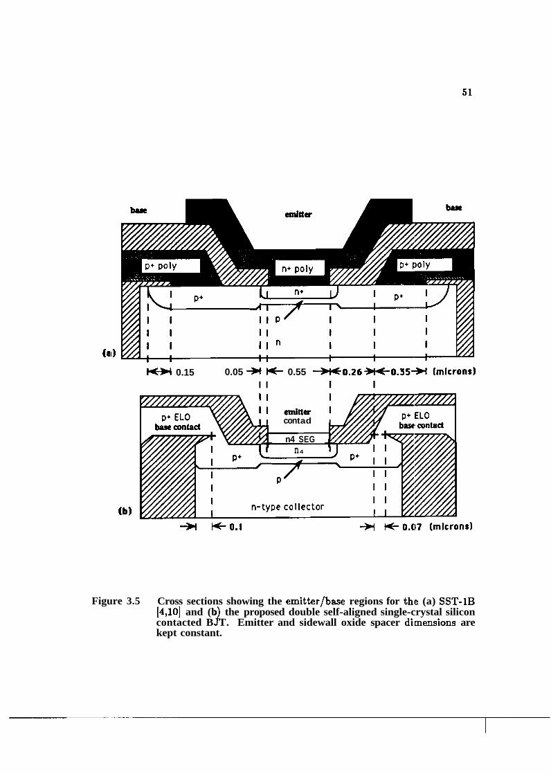
(11)
M 0.15 0.05 * t+ 0.55 -0.26 *O.35-- (microns) I I I I
con tad
n4 SEG n 4
rt 0.1 -fl tt 0.07 (microns)
Figure 3.5 Cross sections showing the emitter/base regions for thle (a) SST-1B [4,10] and (b the proposed double self-aligned single-crystal silicon contacted B 3 T. Emitter and sidewall oxide spacer di:mensions are kept constant.
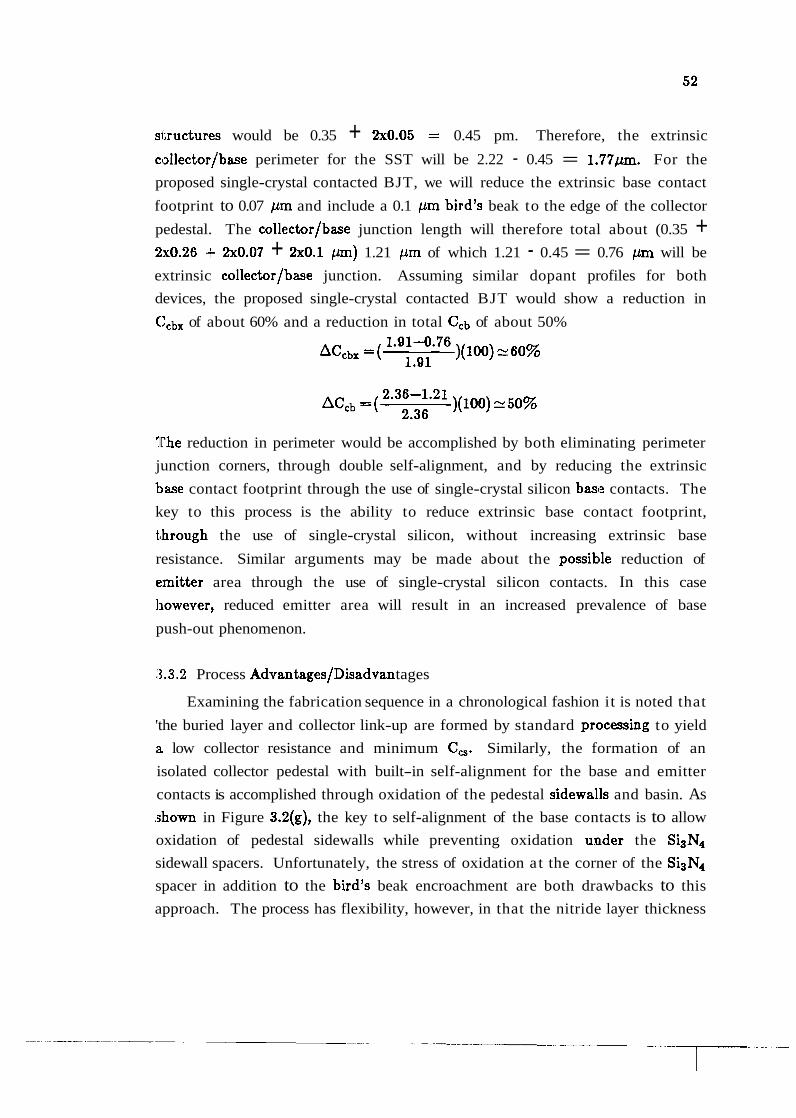
si;ructures would be 0.35 + 2x0.05 = 0.45 pm. Therefore, the extrinsic
collector/base perimeter for the SST will be 2.22 - 0.45 = 1.77pm. For the
proposed single-crystal contacted BJT, we will reduce the extrinsic base contact
footprint to 0.07 pm and include a 0.1 pm bird's beak to the edge of the collector
pedestal. The collector/base junction length will therefore total about (0.35 + 2x026 + 2x0.07 + 2x0.1 pm) 1.21 pm of which 1.21 - 0.45 = 0.76 pm will be
extrinsic collector/base junction. Assuming similar dopant profiles for both
devices, the proposed single-crystal contacted BJT would show a reduction in
Ccbx of about 60% and a reduction in total Ccb of about 50%
The reduction in perimeter would be accomplished by both eliminating perimeter
junction corners, through double self-alignment, and by reducing the extrinsic
base contact footprint through the use of single-crystal silicon base contacts. The
key to this process is the ability to reduce extrinsic base contact footprint,
t,hrough the use of single-crystal silicon, without increasing extrinsic base
resistance. Similar arguments may be made about the possib~le reduction of
emitter area through the use of single-crystal silicon contacts. In this case
llowever, reduced emitter area will result in an increased prevalence of base
push-out phenomenon.
i3.3.2 Process Advantages/Disadvan tages
Examining the fabrication sequence in a chronological fashion it is noted that
'the buried layer and collector link-up are formed by standard prlocessing to yield
,a low collector resistance and minimum C,,. Similarly, the formation of an
isolated collector pedestal with built-in self-alignment for the base and emitter
contacts is accomplished through oxidation of the pedestal sidewa'lls and basin. As ,shown in Figure 3.2(g), the key to self-alignment of the base contacts is to allow
oxidation of pedestal sidewalls while preventing oxidation under the Si3N4
sidewall spacers. Unfortunately, the stress of oxidation a t the corner of the Si3N4
spacer in addition to the bird's beak encroachment are both drawbacks to this
approach. The process has flexibility, however, in that the nitride layer thickness
may be optimized to reduce oxidation stress. One method for creating a bird'-
bea.k-free oxide layer over the side of the collector pedestal would be to use a
version of the sidewall masked isolation (SWAMI) process (981. The SWAMI
process utilizes a nitride layer which covers the exposed silicon pedestal over the
top and along the top portion of the pedestal sidewalls, similar to the BASIC
fabrication process of section 2.4.3.1. When the wafer is oxidized, tlhe oxide layer
grows along the vertical portion of the sidewall with no bird's beak encrouchment
on .the horizontal top portion of the pedestal. The SWAMI process would reduce
coll~ector pedestal width by approximately 0.2 pm when compared to the present
double self-aligned design and could be incorporated into the current process
without the need for additional mask steps.
To provide enhanced structural support for CMP planarizatiori of the EL0
bast: contacts, the EL0 is allowed to nucleate from adjacent seed hole regions
(Figure 3.2(h)). A critical step in this sequence is to insure that a low-defect
merger of the EL0 silicon growth fronts occurs once the fronts intersect one
another. The Hz preclean sequence must remove all oxides from the seed holes
prior to growth. Subsequently, the Ht, HC1, DCS growth sequence must be
accc~mplished without degradation of the exposed collector pedestal sidewall oxide
or CMP SiOp etch stop. To accommodate both needs, growth must be carried
out under well balanced conditions with respect to moisture content, temperature
and pressure as per section 2.2.2. As an alternative to fully E L 0 base contacts,
one may use EL0 for the first part of the contact then use poly to extend the
contact out to the metal interconnect. After growth, CMP planarixation of the
ELC) base contacts will be achieved using a highly uniform thermal Si02 etch
stop. In this case, the most critical parameters are to ensure that first, the silicon
over the etch stop is completely removed and second, that planarization
tolerances across the wafer are as small as possible. Published reports indicate
that 0.01 pm planarization tolerances may be achieved under proper conditions
(991
After planarization, ion implantation of the exposed base conta.cts becomes
an important process parameter. The boron implantation must be shallow
enough to place ions at the wafer surface and the dosage must be high enough to allow for low-temperature impurity-enhanced oxidation. At the same time, the
imp1,ant must be deep enough into the EL0 base contacts so that limited
impurity tnigrotion ia raquircd for the dopants to form the base contact link-up
with the intrinsic base as shown in Figure 3.3(1).
After forming the base contact, the intrinsic device impurity profile must be
implanted and an SEG emitter contact grown. The advantages of growing a
single-crystal SEG emitter include low bulk resistance, a clean interfacial
connection between contact and intrinsic emitter, and reproducibility. As with
the EL0 base contacts, removal of seed hole oxides during Hz preclean will be
balanced against preservation of the thin base contact isolation oxides. In
acldition, the preclean and growth sequences will need to be cariried out at low
temperatures to limit impurity migration within the intrinsic device profile.
Finally, the uniformity of SEG contact thickness across each vvafer and from
wafer-to-wafer will be important for reproducing emitter resistance.
3.3.3 Alternative Emitter Contact Processing
Two potential problems arise as a result of growing an in-situ doped SEG
emitter contact. First, in-situ n-type doping concentrations ( n ~ l s : l ~ ' ~ c r n - ~ ) may
not be high enough to produce a low emitter resistance. This problem may be
easily solved by ion implanting the SEG contacts after growth. Second, ion
implantation damage over the SEG emitter contact seed holes mqy lower material
quality and increase emitter resistance for small emitter areas. One method for
solving both problems simultaneously might be to grow non-seleckive silicon over
the entire wafer prior to arsenic emitter implantation. The result,ing silicon layer
would be single-crystal material over the exposed emitter seed hole and poly-
crystalline over the remaining field oxide. After growth, the wafer could then be
blanket implanted such that the arsenic ions would fill the silicon layer without
substantial penetration through the layer. The non-selective po~lysilicon growth
should provide for more uniform growth over the wafer due to effectively
increasing the seed hole -to- oxide ratio. The non-selective po1y:;ilicon outside of
the emitter trench could be etched away using an additional mask step. The
device would then be rapidly annealed to diffuse the intrinsic emitter from the
~~ilicon contact. Figure 3.6 shows the final stages of device processing with the
modified non-selective emitter contact growth. In this case, the emitter seed holes
are etched as normal, Figure 3.6(a) followed by uniform deposition of poly and
single-crystal silicon and implantation of arsenic (Figure 3.6(b)). Finally, the
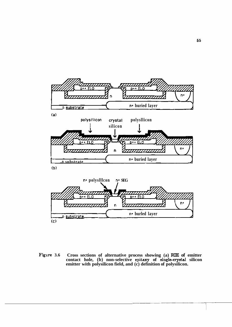
D s u b w a t e n+ buried layer
Polysllicon crystal polysll icon I s i l i con I
t D substrate n+ buried layer
n+ polysll lcon n+ SEG
t D substrate n+ burled layer
t c ) 1
Figure 3.6 Cross sections of alternative process showing (a) RIE of emitter contact hole, (b) non-selective epitaxy of singlt+crystal silicon emitter with polysilicon field, and (c) definition of polysilicon.
unwanted poly is etched away followed by diffusion and anneal of the arsenic
impurities (Figure 3.6(c)).
3.4 Summary
In summary, design drawings and alternative design methods have been
presented for the fabrication of a single-crystal silicon contacted double self-
aligned BJT. In the absence of trench isolation, the fabrication process uses 7
lithography steps. The modified non-selective emitter process may require 8 steps.
This number compares favorably with the state-of-the-art single self-aligned
"SST-1B" process a t 7-8 steps (101, and the double self-aligned "BASIC" process at
6-7 steps (81. Overall, the process requires 2 selective epitaxy sequences and
acldresses the use of SEG and E L 0 in advanced devices. Critical issues have been
identified as E L 0 growth and planarization of extrinsic base contacts, selective
oxidation of base contacts and formation of the intrinsic emitter/base impurity
PI-ofile with reduced temperature processing constraints.
CHAPTER 4
PROCESS DEVELOPMENT
4.1. Overview and Purpose
Chapter 4 will detail the microelectronic fabrication proces development
which has been used to demonstrate feasibility for the proposed fu1,ly self-aligned
BJT. To fabricate devices and test structures, a set of 8 chrome plated masks
were fabricated to perform contact lithography. From the mask set, large area
substrate BJTs were fabricated to serve as a base line process. Large area single
sellf-aligned transistors (SSTs) were then fabricated using SEC; silicon base
contacts to examine the self-aligned emitterlbase junction. Large area double
self-aligned transistors (DSTs) were then fabricated to show feasibility for the full
device and to examine CCb and CEB. Finally, the mask set was used to fabricate
test structures including intrinsic base sheet resistors, intrinsic base pinch
resistors, polycrystalline silicon emitter resistors, and extrinsic base contact
resistors.
To examine specific structural characteristics, spreading resistance profiles
(SRP) were used to determine junction depths and doping concentrations for
large area junctions. Scanning electron microscopy (SEM) was used to examine
device cross sections after fabrication and testing. SUPREM-IV twedimensional
computer simulations of the fabrication process were compared with SRP and
SEM data to calibrate the simulation tools.
4.2 Processing Tools
Figure 4.1 shows an overview of the 8 level mask set used in this research.
Each mask is composed of 144 die with an area of 0.4 x 0.4 cm2. The die were
stepped evenly over each 4 inch lithographic plate except for 5 die 1.ocations which
were left open for large area SRP regions. Each die contains 4 !substrate BJTs
with 5 x 85 pm2 emitters, 4 self-aligned BJTs with 2.4 x 50.4 pm2 emitters
(defined here as type I), and 8 self-aligned BJTs with 4.4 x 84.4 pm2 emitters
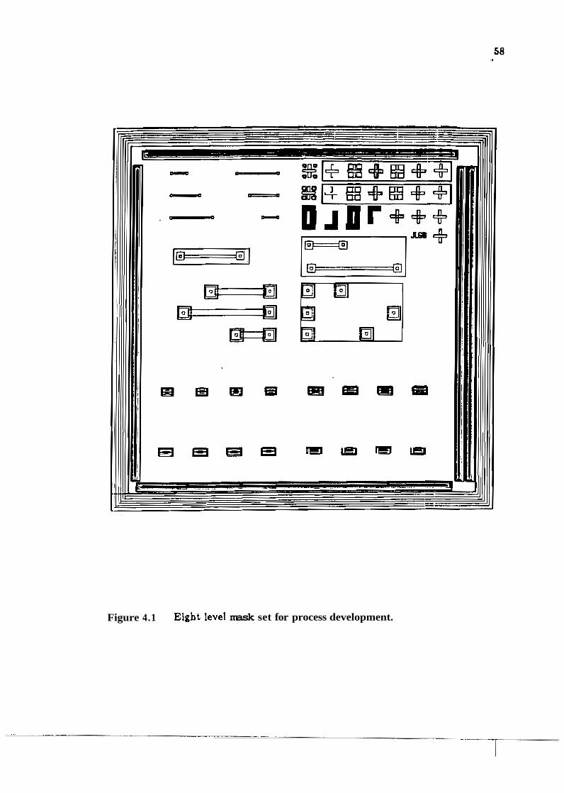
Figure 4.1 Eight level mask set for process development.
(defined here as type 2). Depending upon the process sequence, these self-aligned
BJ'I' areas may produce either SSTs or DSTs. Due to processing difficulties which
were not anticipated during the design of the masks, it became impossible to
fabricate the substrate devices on the same wafer as the self-aligned devices. It also became impossible to obtain SRP areas on the same wafer as the self-aligned
devices due to the need to rearrange the order and and use of mask levels. SRPs
were only possible for substrate BJT wafers.
Each die also contains resistor test structures which are grouped into sets of
three resistors which have 10, 20, and 30 unit squares each so that contact
resistance may be extracted from the sheet resistance. Base pinch resistors, base
sheet resistors (no emitter diffusion), emitter polycrystalline silicon sheet resistors,
and, extrinsic base contact resistors are also used. Each die contains long self-
aligned devices which extend around the perimeter of the die so that they may be
easily cross sectioned for SEM examination. For mask to mask alignment, each
die contains alignment marks which allow registration between all levels.
Fabrication of devices was performed in the Electrical Engineering Solid
State Laboratory and in the Potter Epitaxial Facility. Criticis1 processing
equipment included the Gemini I vertical reduced pressure CVD reactor used to
grow SEG and EL0 over a range of temperature and pressure conditions. The
Gernini I uses a quartz bell jar which covers a Sic coated graphite susceptor. The
susceptor rotates during epitaxy to provide even temperature distritbution. The
susceptor is heated inductively using a radio frequency coil located under the bell
jar. SEG and EL0 growth in the reactor is accomplished using dichlorosilane
(DM), HCl, and H2 gasses which are injected upward through the center of the
susceptor. Other critical processing equipment includes an A[M 210 Ion
Implanter, Drytek 100 Reactive Ion Etcher, Perkin Elmer AlSiCu Sputtering
System, and low pressure CVD system containing CVD polycrystalline silicon and
CVD silicon nitride deposition tubes. Measurement equipment includes a 25keV
Scanning Electron Microscope and a Nomarski Interference Microscope.
To predict process behavior, the Stanford University PRocess EMulator
verzrion IV (SUPREM-IV) was used to create tw-dimensional models of all
process sequences [100,101]. SUPREM-IV implements discretized versions of the
standard equations which govern processes such as oxidation and ion
implantation. The region under simulation is divided into a grid and the
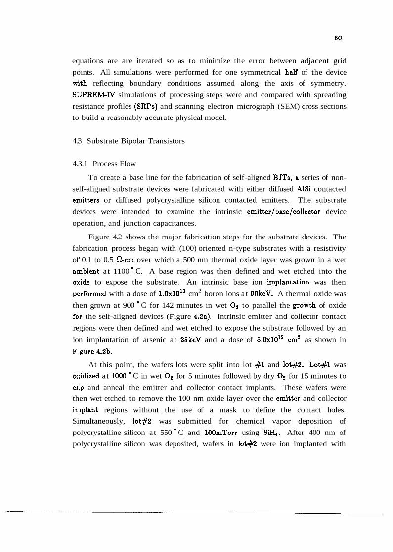
equations are are iterated so as to minimize the error between adjacent grid
points. All simulations were performed for one symmetrical half of the device
with reflecting boundary conditions assumed along the axis of symmetry.
SIJPREM-N simulations of processing steps were and compared with spreading
resistance profiles (SRPs) and scanning electron micrograph (SEM) cross sections
to build a reasonably accurate physical model.
4.3 Substrate Bipolar Transistors
4.3.1 Process Flow
To create a base line for the fabrication of self-aligned BJTs, ,a series of non-
self-aligned substrate devices were fabricated with either diffused AlSi contacted
emitters or diffused polycrystalline silicon contacted emitters. The substrate
devices were intended to examine the intrinsic emitter/base/collector device
operation, and junction capacitances.
Figure 4.2 shows the major fabrication steps for the substrate devices. The
fabrication process began with (100) oriented n-type substrates with a resistivity
of' 0.1 to 0.5 n c m over which a 500 nm thermal oxide layer was grown in a wet
ambient a t 1100 C. A base region was then defined and wet etched into the
oxide to expose the substrate. An intrinsic base ion implanta.tion was then
performed with a dose of 1.0x1013 cm2 boron ions a t 9OkeV. A thermal oxide was
then grown at 900 C for 142 minutes in wet 0 2 to parallel the growth of oxide
for the self-aligned devices (Figure 4.2a). Intrinsic emitter and collector contact
regions were then defined and wet etched to expose the substrate followed by an
ion implantation of arsenic at 25keV and a dose of 5.0x1015 cm2 as shown in
Fiigure 4.2b.
At this point, the wafers lots were split into lot #1 and lot#2. Lot#l was
oxidized a t 1000 C in wet O2 for 5 minutes followed by dry 0 2 for 15 minutes to
cap and anneal the emitter and collector contact implants. These wafers were
then wet etched to remove the 100 nm oxide layer over the emitter and collector
implant regions without the use of a mask to define the contact holes.
Simultaneously, lot#2 was submitted for chemical vapor deposition of
polycrystalline silicon a t 550 C and lOOmTorr using S e . After 400 nm of
polycrystalline silicon was deposited, wafers in lot#2 were ion implanted with
(a) I n- substrate ( 100) 1
base emitter base collector
(c) ( n- substrate ( 100) 1 base emitter base collector
( d l 1 n- substrate ( 100) I
Figure 4.2 Process flow for substrate BJTs showing (a) intrinsic base, (b emitter and collector contact, (c) final structure for Al-contacte emitter BJT, and (d) polysilicon-contacted emitter BJ1C.
d
arsenic to a dose of 5.0~10'~ cm2 at 120 keV and oxidized a t 1000 C in wet O2
for 5 minutes followed by 15 minutes of dry 02. These wafers were then wet
etched to remove the oxide over the polycrystalline silicon and, the poly was
defined and etched to form emitter and collector contacts. Base contact holes for
both wafer lots were then defined, implanted with boron to a dose of 1.0~10'~
crn2 at 25keV, and annealed a t 900 C for 10 minutes in dry 02. Following a
B:HF dip to remove oxides in the contact holes, a lifboff pattern was defined on
both wafer lots, AlSiCu was sputter deposited, lifted off, and the remaining metal
was annealed a t 415 ° C to form ohmic contacts. The final crloss-sections are
shown in Figure 4 . 2 ~ and d.
4.3.2 Structural Data and Simulations
Spreading resistance profiles (SRP) for the polysilicon contacted substrate
dlevices were performed through the intrinsic emitter/base/coll~ector region to
determine junction depths. Figure 4.3 shows the SRP along with a SUPREM-N
simulation. SUPREM-N simulations and SRP data are shown to agree reasonably
well on emitter and base junction depth but disagree on peak junction doping
levels. Differences in the junction depth and peak doping may be account for by
errors in the accuracy of the SRP measurement including errors in the sample
bevel angle and step width. The SUPREM-N simulation could be off with
rlespect to the actual furnace temperature which was used in processing the
devices and the exact moisture species which was present in the furnace during
oxidation. Differences in diffusion coefficients or defect models cou.ld easily change
junction depths dramatically. The general agreement is good in this case.
4.4 Self-Aligned Emitter Bipolar Transistors
4,.4.1 Process Flow
To examine the self-aligned emitter portion of the proposed 13JT without the need to fabricate the collector pedestal, devices were fabricated .which used SEG
silicon extrinsic base contacts. Figure 4.4 shows the major processing steps for
these single self-aligned devices. The process began with identical (100) substrates
used in fabricating the substrate BJTs. A 500 nm oxide layer was grown over
these wafers at 1100 C in a wet ambient. Mask level 1 was then defined and the

I0 19
lo
I0 ' 7
n collector
1015 I I I
! I I 1 0 ' 4 ~ . . - . ! - - ' - - . - - . - ~ - - - -
n+ emltter I I I I
n collector
4
Figlure 4.3 Spreading resistance profile (a) of polysilicon contacted substrate BJT and (b) SUPREM-N simulation. Emitter area was 5 x 85 pm2 for the devices.
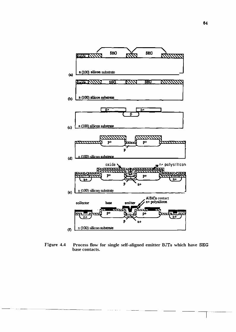
P - (dl n (100) silicon s u b s m I
(3
oxide , n+ polysllicon
n (100) silicon substrate 1
(el n ( 1 0 ) silicon substrate I AlSiCu contact
ernit= /n+polyaam
(O 1 n (100) silicon s u b s m ~ I
Figure 4.4 Process flow for single self-aligned emitter BJTs which have SEG base contacts.
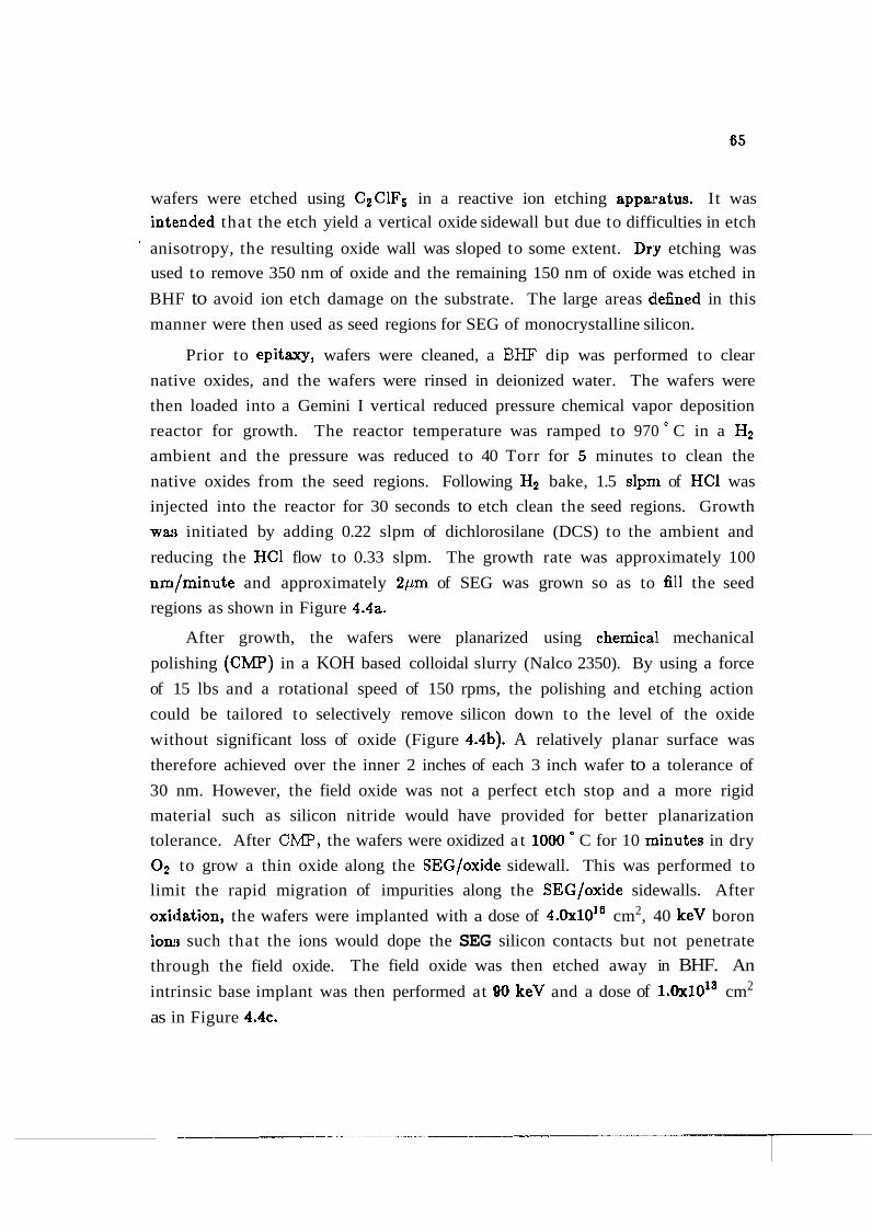
wafers were etched using C2C1F5 in a reactive ion etching appa1:atus. It was intlended that the etch yield a vertical oxide sidewall but due to difficulties in etch
a anisotropy, the resulting oxide wall was sloped to some extent. Dr;y etching was
used to remove 350 nm of oxide and the remaining 150 nm of oxide was etched in
BHF to avoid ion etch damage on the substrate. The large areas defined in this
manner were then used as seed regions for SEG of monocrystalline silicon.
Prior to epitaxy, wafers were cleaned, a BHF dip was performed to clear
native oxides, and the wafers were rinsed in deionized water. The wafers were
then loaded into a Gemini I vertical reduced pressure chemical vapor deposition
reactor for growth. The reactor temperature was ramped to 970 ° C in a Hz
ambient and the pressure was reduced to 40 Torr for 5 minutes to clean the
native oxides from the seed regions. Following Hz bake, 1.5 slpnl of HCl was
injected into the reactor for 30 seconds to etch clean the seed regions. Growth
wai3 initiated by adding 0.22 slpm of dichlorosilane (DCS) to the ambient and
reducing the HCl flow to 0.33 slpm. The growth rate was approximately 100
nm/minute and approximately 2pm of SEG was grown so as to fill the seed
regions as shown in Figure 4.4a.
After growth, the wafers were planarized using chemical mechanical
polishing (CMP) in a KOH based colloidal slurry (Nalco 2350). By using a force
of 15 lbs and a rotational speed of 150 rpms, the polishing and etching action
could be tailored to selectively remove silicon down to the level of the oxide
without significant loss of oxide (Figure 4.4b). A relatively planar surface was
therefore achieved over the inner 2 inches of each 3 inch wafer to a tolerance of
30 nm. However, the field oxide was not a perfect etch stop and a more rigid
material such as silicon nitride would have provided for better planarization
tolerance. After CMP, the wafers were oxidized a t 1000 ° C for 10 minutes in dry
O2 to grow a thin oxide along the SEG/oxide sidewall. This was performed to
limit the rapid migration of impurities along the SEG/oxide sidewalls. After
oxitlation, the wafers were implanted with a dose of 4 . 0 ~ 1 0 ' ~ cm2, 40 keV boron
iom3 such that the ions would dope the SEG silicon contacts but not penetrate
through the field oxide. The field oxide was then etched away in BHF. An
intrinsic base implant was then performed at 90 keV and a dose of 1 . 0~10 '~ cm2
as in Figure 4.4~.
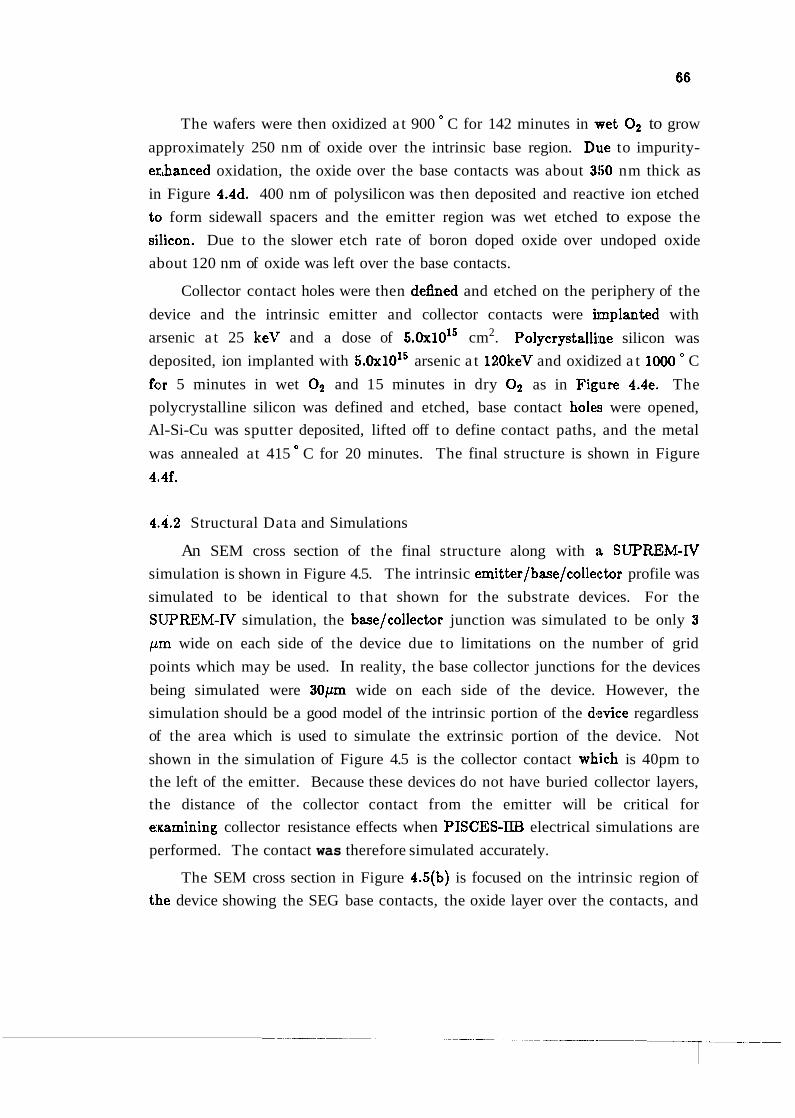
The wafers were then oxidized a t 900 ' C for 142 minutes in wet O2 to grow
approximately 250 nm of oxide over the intrinsic base region. Due to impurity-
enhanced oxidation, the oxide over the base contacts was about 3!i0 nm thick as
in Figure 4.4d. 400 nm of polysilicon was then deposited and reactive ion etched
to8 form sidewall spacers and the emitter region was wet etched to expose the
sillicon. Due to the slower etch rate of boron doped oxide over undoped oxide
about 120 nm of oxide was left over the base contacts.
Collector contact holes were then defined and etched on the periphery of the
device and the intrinsic emitter and collector contacts were implanted with
arsenic a t 25 keV and a dose of 5.0x1015 cm2. Polycrystalli~ne silicon was
deposited, ion implanted with 5.0x101' arsenic a t 120keV and oxidized a t 1000 ' C
fclr 5 minutes in wet 0 2 and 15 minutes in dry 0 2 as in Fig.ure 4.4e. The
polycrystalline silicon was defined and etched, base contact holes were opened,
Al-Si-Cu was sputter deposited, lifted off to define contact paths, and the metal
was annealed at 415 C for 20 minutes. The final structure is shown in Figure
4.4f.
4..4.2 Structural Data and Simulations
An SEM cross section of the final structure along with :% SUPREM-TV
simulation is shown in Figure 4.5. The intrinsic emitter/base/collector profile was
simulated to be identical to that shown for the substrate devices. For the
S'UPREM-N simulation, the base/collector junction was simulated to be only 3
pm wide on each side of the device due to limitations on the number of grid
points which may be used. In reality, the base collector junctions for the devices
being simulated were 30pm wide on each side of the device. However, the
simulation should be a good model of the intrinsic portion of the device regardless
of the area which is used to simulate the extrinsic portion of the device. Not
shown in the simulation of Figure 4.5 is the collector contact which is 40pm to
the left of the emitter. Because these devices do not have buried collector layers,
the distance of the collector contact from the emitter will be critical for
eaamining collector resistance effects when PISCES-IIB electrical simulations are
performed. The contact was therefore simulated accurately.
The SEM cross section in Figure 4.5(b) is focused on the intrinsic region of
the device showing the SEG base contacts, the oxide layer over the contacts, and
base em1 t te r
collector
t--- -0 -------- ---
n- collector & substrate 1 (a) device w i d t h ( ~ ~ r n )
Figure 4.5 Scanning electron micrograph cross section and SWREM-IV computer simulation of the SEG base contacted self-aligned emitter BJTs.
the polycrystalline silicon emitter contact. For this SEM, the sample was diced to expose the edge and the oxide was removed to reduce electron cb.arging. As can
be seen, the oxide layer over the base contacts remained intact after forming the
self-aligned emitter. However, the upper corner of the base contact is nearly
shorting out to the polysilicon emitter where the oxide is thinnes;t. This area is
the weakest portion of the base contact isolation and must be improved by
enhancing the oxidation rate over the base contacts or by rounding the corner of
the base contact prior to oxidation.
4.5 Double Self-Aligned Transistors
4.,5.1 Process Flow
Processing for the fully self-aligned devices was very similar to that of the
self-aligned emitter devices and is shown in Figure 4.6. The process is essentially
identical to the fabrication process for the proposed scaled-down version of the
dsevice as shown in Figure 3.1. Only the major process steps will therefore be
sliown here. A 500 nm oxide layer was grown over (100) n-type sctbstrates with a
resistivity of 0.1 to 0.5 Stcm. A 400 nm layer of low pressure chemical vapor
dleposition silicon nitride was then deposited over the wafer ;at 777 ' C and
4(30mTorr. Mask 1 was then defined and the silicon nitride layer was vertically
etched using SF6 at 500 watts and 260 mTorr. Upon reaching the oxide layer,
tlie etch gas was changed to C2C1F5 and the oxide layer was etc:hed down to a
tliickness of 150 nm. Wet etching was then performed to remove the remaining
oxide down to the substrate (Figure 4.6a). A 20 nm stress relief oxide layer was
grown at 1000 a C for 10 minutes in dry 0 2 followed by the deposition of 400 nm
of low pressure CVD silicon nitride. The wafers were then vertically etched down
to the stress relief oxide using SFB to form nitride sidewall spacers. After
removing the stress relief oxide, the substrates were etched down 500 nm in
C2CLF5 plasma as in Figure 4.6b. The wafer was then oxidized at 1000 in wet
Oz for 50 minutes to grow 340 nm of oxide over the collector pedestal.
Following oxidation, the nitride was removed in boiling Hl3PO4 and the
exposed thin stress relief oxide was removed in BHF to create self-aligned seed
holes for the extrinsic base contacts. Wafers were then divided into lot#l and
lot#2. Lot#l was submitted for epitaxial lateral overgrowth of silicon. Wafers
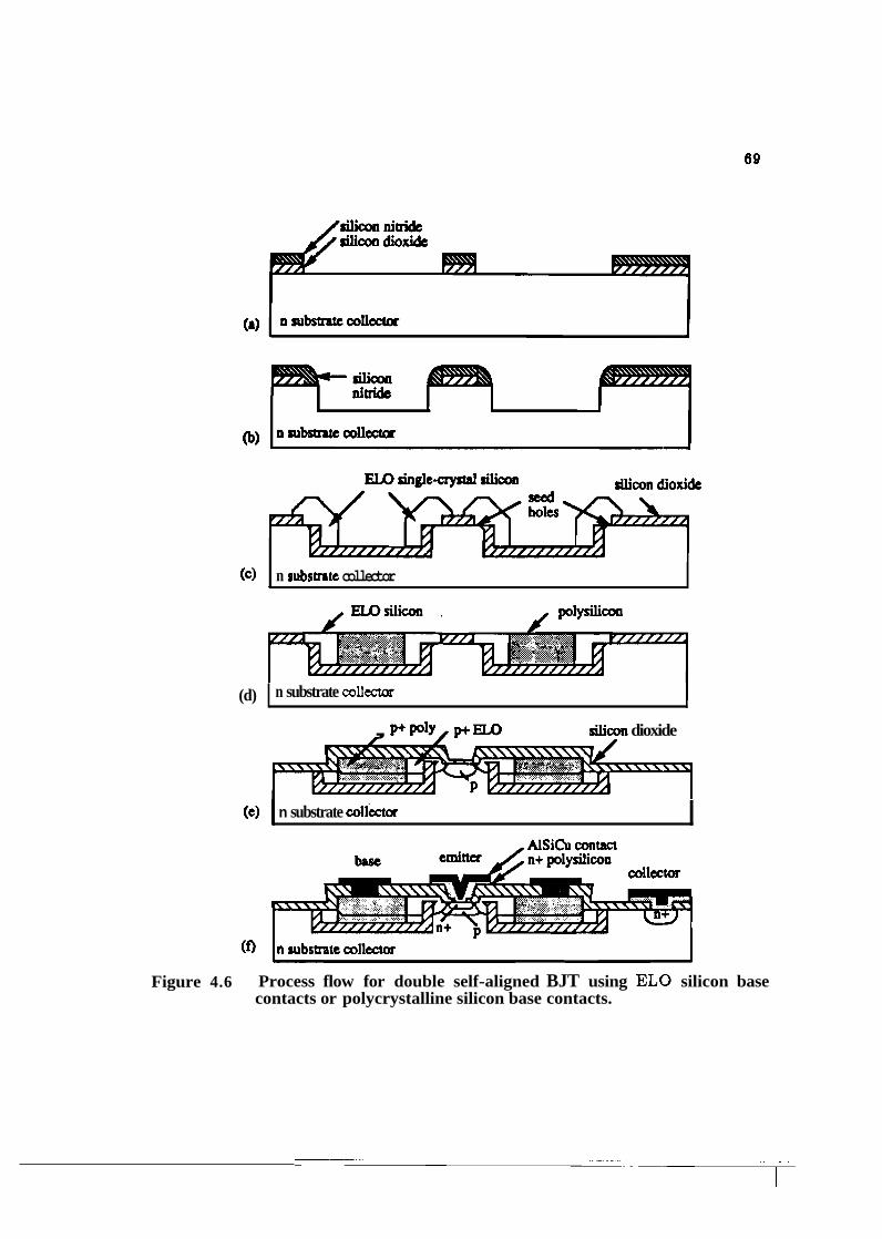
n subsarte collector
, P+P~Y, WELO silim dioxide
(d)
(e) I n substrate colktor I
n substrate collectat I
Figure 4.6 Process flow for double self-aligned BJT using EL0 silicon base contacts or polycrystalline silicon base contacts.
were loaded into the reduced pressure CVD reactor and the temperature was
ramped to 970 a C a t atmospheric pressure. Upon reaching 970 a (Z , the pressure
was reduced to 40 Torr for a 5 minute H2 bake to remove native oxides.
Following the H2 bake, HCl was added to the ambient for a 30 w:cond etch and
growth was initiated by the addition of DCS. Conditions for the growth were 40
Talrr, 970 C, 0.22 slpm of DCS, 0.33 slpm of HC1 and 60 slpm of H2 with a
growth rate of 100 nm/minute. Approximately 4pm of EL0 was g,rown from the
seed regions as shown in Figure 4 .6~.
Following EL0 growth, wafer lots #1 and #2 received the sa,me processing.
The entire group of wafers received a BHF dip to remove native oxides and 1.2pm
of CVD polycrystalline silicon was deposited a t 550 C and 100 nnTorr to cover
the wafers. The wafers were then chemical mechanically planarized to remove
silicon down to the field oxide etch stop using 15 1bs of force and 150 rpms of
rotation (Figure 4.6d). After CMP, the wafers were oxidized a t :LO00 a C for 10
miinutes in dry 0 2 to oxidize the ELO/oxide interface and reduce rapid migration
of impurities down the interface. The wafers were then implanted with 4 .0~10~ '
cm2 40 keV boron and the field oxide was removed in BHF. M a ~ k 3 was then
defined to expose the emitter region and an intrinsic base implant was performed
using 1 . 0 ~ 1 0 ' ~ cm2 boron a t 9OkeV. At this point, the parasitic b:ue contacts on
the perimeter of the device were removed by plasma etching in SF6.
From this point on, processing of the fully self-aligned devices was identical
to processing of the single self-aligned devices described in section 4.4.1. Briefly,
the wafers were oxidized at 900 C for 142 minutes in wet 0 2 to create the
isolation oxide for the base contacts as in Figure 4.6e. 400 nm of polycrystalline
sil.icon was deposited and vertically etched to form sidewall spacers around the
emitter, and the self-aligned emitter was opened by wet etching. The collector
contact region was defined and the wafers were implanted with 25k:eV arsenic to a
dose of 5 . 0 ~ 1 0 ~ ~ cm2 to form the emitter and collector contact. Polycrystalline
si:licon was the deposited to 400 nm and implanted with l2O:lkeV arsenic to 5.0x10'~ cm2. The wafers were oxidized a t 1000 * C for 5 minutes in wet O2 and
l t i minutes in dry 0 2 , the polycrystalline contacts were defined and etched, base
contact holes were opened, and the devices were metallized. 'The final cross
section is shown in Figure 4.6f. After all processing, the intrinsic
e~nitter/base/collector regions of the substrate and self-a1igne:d devices had
received identical processing except for the AlSiCu contacted substrate devices.
4.5.2 Structural Data and Simulations
SEM cross sections of the device after EL0 growth but before planarization
(see Figure 4 .6~) and after final processing (see Figure 4.6f) are shown in Figure
4.7. The cross section in Figure 4.7a indicates that the seed hole for growth of
the E L 0 were approximately 350 nm and that there was relatively little bird's
beak encroachment from the oxide grown over the collector pedestal. The sharp
faceting of the E L 0 in Figure 4.7a was due to the reduced growth rate of the
(110) planes with respect to the (100) planes. As may be observed, when very
small seed holes are used, the facets may rapidly eliminate the (100) planes all
together and thus slow the growth rate substantially. After fina.1 processing,
Figure 4.7b reveals that the base contact was approximately 240 nm. wide due to
oxidation of the sidewall.
Using the structural data shown in Figure 4.7, a SUPREM-N si~nulation was
performed to model the entire device, including the extrinsic b i ~ e contacts.
Figure 4.8 shows a SUPREM-N cross section of the active device a.rea with the
collector contact not shown. As for the SEG base contacted devices, the collector
contact was simulated to scale and is therefore located 40 pm to the left of the
emitter. To save grid points, only the portion of the base contact which actually
contacts the substrate was modeled. The remaining portion of the base contact
does not influence d.c. electrical behavior and may be assumed to be a very small
resistance. As for the SEG base contacted BJTs, the critical issue is achieving a
low resistance link-up between the diffused portion of the extrinsic base contact
and the intrinsic base without allowing the heavily doped extrinsic base to
encroach significantly on the emitter. This will achieve a low e:rtrinsic base
resistance without degrading the low current operation of the emitter/base
junction.
Figure 4.9 shows SRP profiles through the extrinsic base/colleci;or junctions
for E L 0 and poly-base contacted devices along with SUPREM-IV computer
eimulations. It is observed that while the doping level is about the same for the
single crystal and polysilicon contacts, the junction penetrat6s dee:per into the
substrate for the polysilicon contact. This may be due to the high cliffusion rate
difference between polysilicon and single crystal silicon which would allow boron
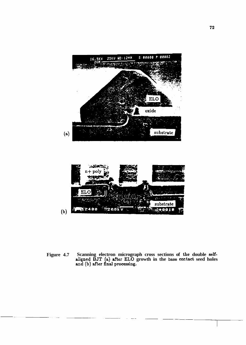
Figure 4.7 Scanning electron micrograph cross sections of the double self- growth in the base conitact seed holes
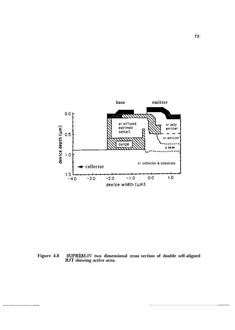
base emitter
n- collector & substrate 4 collector
device wldth (pm)
Figure 4.8 SUPREM-IV two dimensional cross section of double self-aligned BJT showing active area.
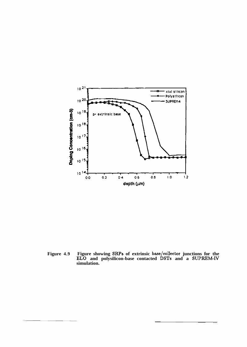
102' - xtal silicon
Figure 4.9 Figure showing SRPs of extrinsic base/collector junctions for the EL0 and polysilicon-base contacted DSTs and a SUPREM-N simulation.
to migrate to the polysilicon/substrate interface faster than to the riingle crystal
silicon/substrate interface. However, the SRP cannot measure the effect of
interfacial contact resistance between the polysilicon and the single crystal silicon
which occurs due to the formation of native or chemically-induced interfacial
oxides.
4.6 Resistor Test Structures
Along with the fabrication of bipolar transistors, resistance test structures
were fabricated to measure extrinsic base sheet resistance, intrinsic: base sheet
resistance, and intrinsic base pinch resistance. All but the first s t~~ucture were
fabricated along side the substrate bipolar transistors on the same wrtfer. For the
E L 0 and polycrystalline silicon extrinsic base contact test structures, separate
wafers were fabricated which contained self-aligned contacts ranging between
about 0.2 pm and 0.4pm. Using resistor bars of different lengths, the sheet
resistance could be isolated from the contact resistance to yield the desired
information to be presented in Chapter 5.
Fabrication steps for the EL0 contact resistance test structures are shown in
Figure 4.10. The polysilicon contact resistor is not shown. Briefly, :p-type (100)
substrates were oxidized at 1100 ' C to grow 500 nm of Si02. The oxide was then
vertically etched down to the substrate and a 20 nm stress relief oxide layer was
grown. CVD silicon nitride was then deposited at 777 ' C to various thicknesses
on different wafers and the nitride was vertically etched to form spacers. The
wafers were then oxidized a t 1000 ' C for 15 minutes in steam to grow 120 nm of
thermal oxide to oxidize the exposed silicon (Figure 4.10a) and the nitride was
removed in &Po4. The wafers were then etched in BHF to remove the thin
stress relief oxides and create seed holes of different sizes. One half of the wafers
were submitted for EL0 silicon growth and the other half were set aside. For
E L 0 growth, the wafers were baked a t 970 ' C in H2 for 5 minute:3 to remove
native oxides, a 30 second HC1 etch was performed and 2pm of EL0 was grown a t
970 ' C and 40 Torr using DCS of 0.22 slpm, HCl of 0.33 slpm, and H:! of 60 slpm
(Figure 4.10b).
After E L 0 growth, all wafers were deposited with 600 nIn of CVD polycrystalline silicon. The wafers were then planarized to the level of the field
oxide (Figure 4.10~). A mask was then used to define and etch 3 resistor bar
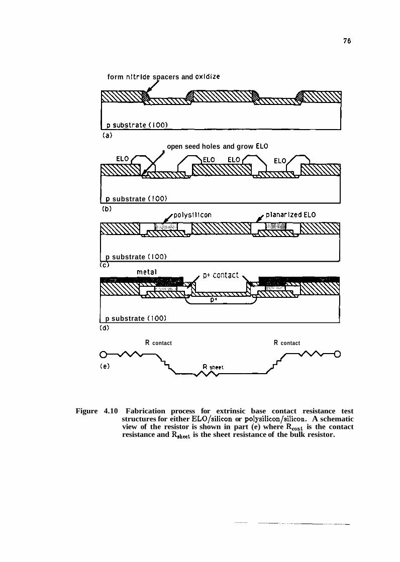
form nl trlde spacers and oxldlze
open seed holes and grow EL0 I
1 p substrate ( 100) I
1 p substrate ( 100) t c 1
I metal - A r r r r+ r r+
1 p substrate ( 100) 1 (d)
R contact R contact
Figure 4.10 Fabrication process for extrinsic base contact resistance test structures for either ELO/silicon or polysilicon/silicon. A schematic view of the resistor is shown in part (e) where RCont is the contact resistance and Rsheet is the sheet resistance of the bulk resistor.

structures with 10, 20, and 30 squares of length. The EL0 or polysilicon regions
were used as the contacts for these resistor bars. The -wafers were then ion
implanted with 4OkeV boron to a dose of 4 . 0 x 1 0 ~ ~ c m ~ to simulate the base
contacts. The wafers were then oxidized for 142 minutes a t 900 ' C: in wet 02,
oxidixed a t 1000 ' C for 5 minutes in wet O2 and for 15 minutes at, 1000 ' C in
dry Oz to simulate thermal processing of the BJTs. No emitter ion implantation
or polysilicon emitter contact processing was performed. Following thermal
processing, contact holes were opened and A1 contacts were deposited and
annealed a t 430 ' C for 20 minutes to insure good contact resistance between the
metal and E L 0 silicon (or metal/polysilicon) (Figure 4.10d). A schematic
diagram of the resistor is given in Figure 4.10e where RmntaCt is the desired
quantity. SEM cross sections were used to determine the actual width of contacts
on the substrate.
4.7 Summary
Process development for the fully self-aligned bipolar transistor may be
separated into four primary objectives. First, substrate devices were fabricated to
establish a viable intrinsic dopant profile. Second, single self-aligned transistors
were fabricated utilizing SEG base contacts to establish feasibility for use of
boron impurity-enhanced oxidation as a self-alignment technique. Third, double
self-aligned bipolar transistors utilizing either combined ELO/polycrystalline
silicon extrinsic base contacts or fully polycrystalline silicon ex-trinsic base
contacts were fabricated to demonstrate that the self-aligned collector pedestal
was feasible in conjunction with the self-aligned emitter/base. Forth, comparison
of SUPREM-IV process simulations to experimental data was used to validate the
simulation tools so that a reasonably accurate model of the fully scaled device
could be achieved.
CHAPTER 5
ELECTRICAL MEASUREMENTS
5.1 Overview and Purpose
Chapter 5 will describe d.c. and ax. electrical measurements as well aa
PISCES-ID3 computer simulations of the bipolar transistors and, resistor test
sl;ructures discussed in chapter 4. Bipolar transiston were lneasured for
n~aximurn d.c. current gain (hFE-rnar), junction ideality (q), revense breakdown
voltage (BVcBo) and (BVBEo), early voltage (VA), reverse biased junction leakage
current (IR), and collector to emitter breakdown voltage (BVcEo). Intrinsic and
extrinsic collector/base capacitance (Ccbi and Ccbr) were extracted from substrate
slid SST BJTs. Ccb was not measured directly from double elf-aligned BJTe
because the capacitance values would have been below the range of detection for
th.e capacitance meter. Emitter/base capacitance Ceb was measured directly from
S8Ts and DSTs. Contact resistance of ELO/silicon and polys~ilicon/eilicon
interfaces were measured for different contact areas. PISCES-IIB device
sixnulations were compared with measured data to validate the use of simulations
in predicting the performance of scaled-down transistor designs.
5.2 Measurement Tools
D.c. measurements were performed using an H.P. 4145A digital parameter
analyser. Devices were probed directly on each wafer using low resistance metal
probes. A vacuum stage was used to hold the samples in place and dry No was
passed over the devices under test. The leakage and inherent noiee within the
probe system and parameter analyser were less than 10 pA with the eyetern a t
300" K and no illumination. A.c measurements were performed using an HP 42ir5A Mutifrequency LCR Meter connected to a micromanipulator probe station.
Th'e LCR meter was calibrated internally before each measurement $0 eliminate
caplacitance associated with the probe tips.
To model the electrical nature of the eelf-aligned BJTs, PISCES-IIB tw*
dimensional computer simulations were performed using input from the
SUPREM- IV process simulator. PIS CES-IIB (PoISson and Continuity Equation
Solver) solves Poisson's equation and the current continuity equations for holes
and electrons in a self-consistent iterative manner. Solutions are iterated between
adjacent grid points as defined by the SUPREM-IV simulation output. The grid
or mesh was refined around rapidly varying dopant concentrations to improve
convergence. PISCES-IIB is limited to simulations of devices which do not
demonstrate quantum mechanical transport through the quasi-neutral base such
as a resonate tunneling BJT or thin base HBT. In all cases, Boltzman carrier
statistics were assumed to speed simulation time. All simulations included
modeling of bandgap narrowing, Scbockley-Read-Hall recombination generation,
Auger recombination, and field and concentration -dependent mobility. All simulations were for one symmetrical half of the full device with the axis of
symmetry acting as a mirror boundary.
5.3 D.C. Measurement
5.3.1 Data Summary
Tables 5.1 and 5.2 list average d.c. parametric data taken from substrate,
SST, and DST BJTs. Average q factors were determined by the averaging the
point-tepoint q factors over a t least one decade of current. BVcBo and BVEBo
were measured as the voltage a t which the reverse bias current increased rapidly
and reached 1pA for basejemitter junctions and 10pA for base/collector junctions. BVcEo was measured as the voltage a t which Ic reached lo&. It was
very important to meaaure BVCEo in complete darkness. Any light was found to change breakdown voltages, presumable by generating carriers in the depletion
regions. V, was measured by plotting Ic against VCE for increasing IB steps then
extrapolating the -VCE intercept of a line drawn collinear with one of the Ic
curves in the forward active region where Ic 1: 0.5mA. RB was measured between
15 and 30mV to determine the value of the intrinsic base sheet resistance for
substrate BJTs only. Junction leakage currents were measured using the Hi' 4145A. Results are listed in Table 5.2.
Table 5.1 D.c. electrical data for Al contacted substrate BJTe (Al-sub), polyeilicon contacted substrate BJTs (P-sub), SST's, EL0 base contacted DSTs (E-DST), and polysilicon base contacted DSTs (P- DST). Emitter junction areas were 2.4 x 50.4pm--* and 4.4 x 84.4prn-*.
': best device8
*:* pinch resistors were not possible for the SST and DST using thia mask set.
Parameter
samples
h ~ ~ - m u ?h QIc
BVBEO (V) BVBCO (V) BV-0 (V) VA (V) RB (kn/D)
EDST
38
100
(1.01*) 1.04
(1.04*) 1.25
-10
N-90
25
-22 * *
- P-DST
2 1
162
1.05
1.25
-11
*90
23
-36 * *
Al-sub
21
30
1.02
1.16
-11
-60
58
-67
13.3
P-sub
30
170
1.01
1.12
-11
-60
58
-66
8.5
SST
39
102
1.01
1.02
-10
-40
38
-65 **
Table 5.2 Area dependent junction leakage currents for devices listed in Table 5.1 with emitter areas of 2.4 x 50.4+m2 (type 1) and 4.4 x 84.4pm2
(type 2).
E-B area
(~cm-~)
425
425
121
370
121
370
121
370
transistor
Al-sub
P-sub
SST type 1
SST type 2
E-DST type 1
E-DST type 2
P-DST type 1 P-DST type 2
C-B area
( P - ~ )
7500
7500
7215
9425
180
470
180
470
ICB (PA)
18
5
50
60
300
300
300
300
IEB (PA)
3
3
27
88
30
90
30
82
JCB
( A / c ~ - - ~ )
2.4e-7
6.7e-8
6.9e-7
6.4e-7
1.67e-4
6.4e-5
1.67e-4
6.4e-5
JEB
( ~ / c m - ~ )
7e-7
7e-7
2.2e-5
2.4e-5
2.5e-5
2.4e-5
2.5e-5
2.2e-5
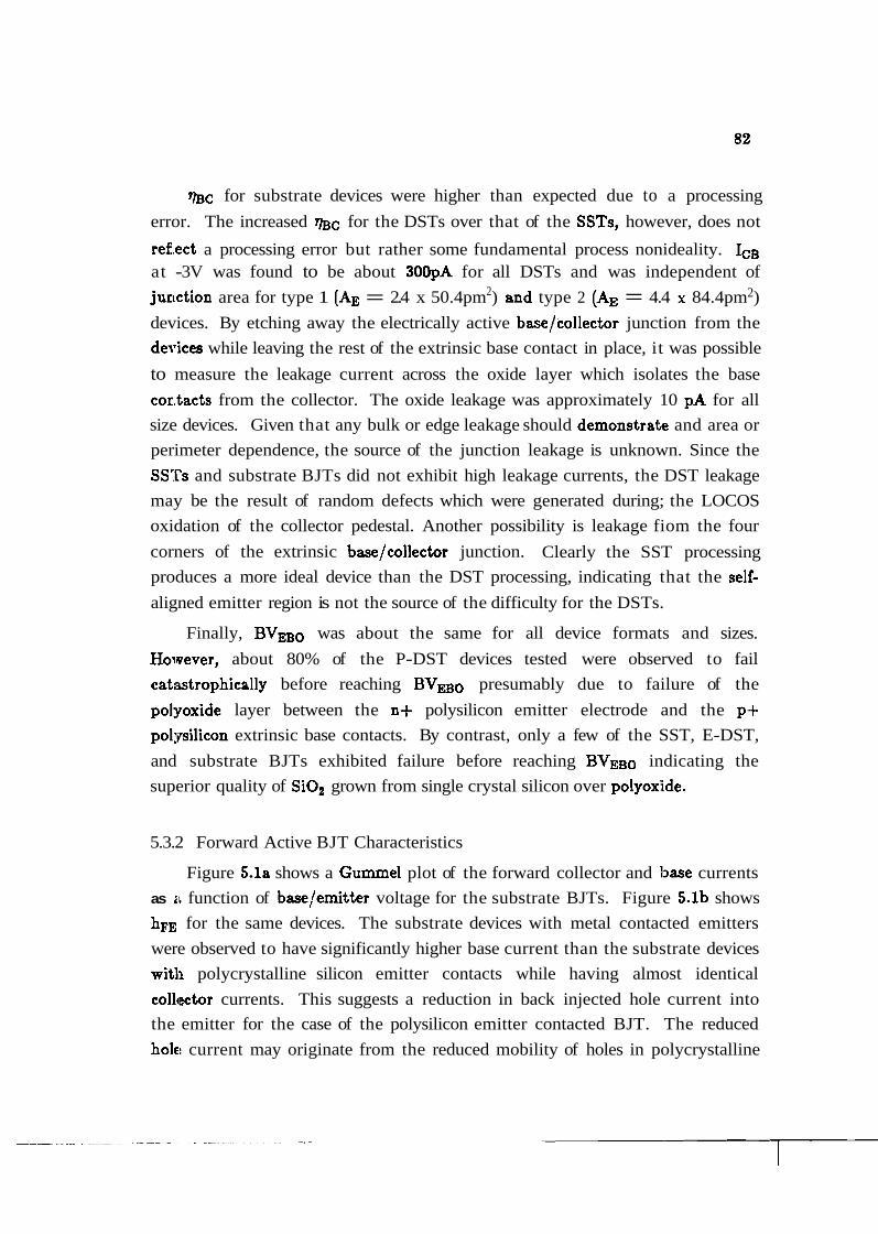
QJC for substrate devices were higher than expected due to a processing
error. The increased ~c for the DSTs over that of the SSTs, however, does not
reflect a processing error but rather some fundamental process nonideality. ICB at -3V was found to be about 300pA for all DSTs and was independent of
juc~ction area for type 1 (AE = 2.4 x 50.4pm2) and type 2 (AE = 4.4 x 84.4pm2)
devices. By etching away the electrically active base/collector junction from the
devices while leaving the rest of the extrinsic base contact in place, it was possible
to measure the leakage current across the oxide layer which isolates the base
conitacts from the collector. The oxide leakage was approximately 10 pA for all
size devices. Given that any bulk or edge leakage should dem~nstrat~e and area or
perimeter dependence, the source of the junction leakage is unknown. Since the
SSTs and substrate BJTs did not exhibit high leakage currents, the DST leakage
may be the result of random defects which were generated during; the LOCOS
oxidation of the collector pedestal. Another possibility is leakage fiom the four
corners of the extrinsic base/collector junction. Clearly the SST processing
produces a more ideal device than the DST processing, indicating that the self-
aligned emitter region is not the source of the difficulty for the DSTs.
Finally, BVEBo was about the same for all device formats and sizes.
Hoiwever, about 80% of the P-DST devices tested were observed to fail
cat;~trophically before reaching BVEBo presumably due to failure of the
polyoxide layer between the n+ polysilicon emitter electrode and the p+
po1:vsilicon extrinsic base contacts. By contrast, only a few of the SST, E-DST,
and substrate BJTs exhibited failure before reaching BVEBo indicating the
superior quality of SiOp grown from single crystal silicon over polyoxiide.
5.3.2 Forward Active BJT Characteristics
Figure 5.la shows a Gummel plot of the forward collector and lbase currents
as zr function of baselemitter voltage for the substrate BJTs. Figure 5.lb shows
hFE for the same devices. The substrate devices with metal contacted emitters
were observed to have significantly higher base current than the substrate devices
with polycrystalline silicon emitter contacts while having almost identical
coll~ector currents. This suggests a reduction in back injected hole current into
the emitter for the case of the polysilicon emitter contacted BJT. The reduced
hole current may originate from the reduced mobility of holes in polycrystalline
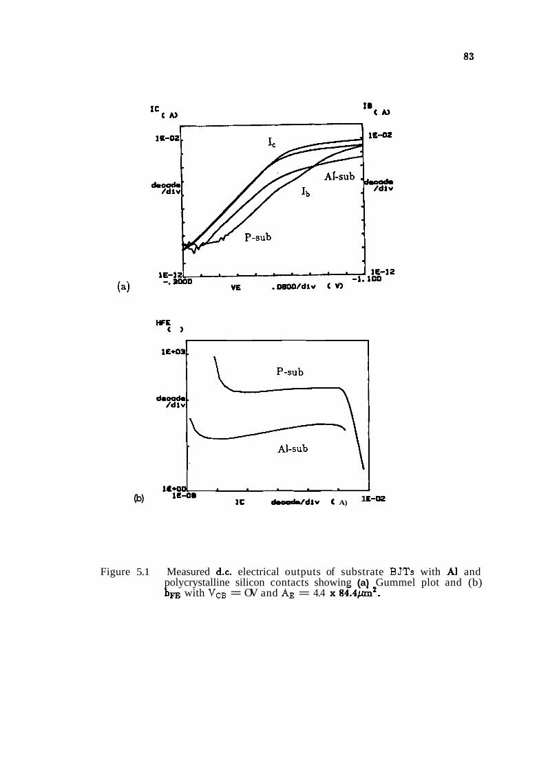
1 t* (b) le4' 1 E-02 1C dmoodddlv i A)
Figure 5.1 Measured d.c. electrical outputs of substrate BJTs with A1 and polycrystalline silicon contacts showing (a) Gummel plot and (b) hFE with VCB = OV and AE = 4.4 x 84.4pm2.
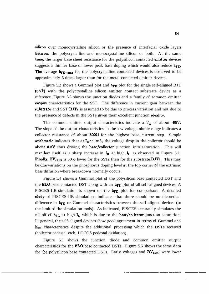
silic:on over monocyrstalline silicon or the presence of interfacial oxide layers
betlween the polycrystalline and monocrystalline silicon or both. At the same
time, the larger base sheet resistance for the polysilicon contacted e:mitter devices
suggests a thinner base or lower peak base doping which would also reduce hFE.
The average hFE-max for the polycrystalline contacted devices is observed to be
approximately 5 times larger than for the metal contacted emitter devices.
Figure 5.2 shows a Gummel plot and hFE plot for the single self-aligned BJT
(SS'I') with the polycrystalline silicon emitter contact substrate device as a
reference. Figure 5.3 shows the junction diodes and a family of cornmon emitter
out1)ut characteristics for the SST. The difference in current gain between the
sub:strate and SST BJTs is assumed to be due to process variation and not due to
the presence of defects in the SSTs given their excellent junction ideality.
The common emitter output characteristics indicate a VA of about -65V.
The slope of the output characteristics in the low voltage ohmic range indicates a
collector resistance of about 600n for the highest base current step. Simple
aritlhmetic indicates that a t Ic= lmA, the voltage drop in the collector should be
about 0.6V thus driving the base/collector junction into saturation. This will
manifest itself as a sharp increase in IB at high Ic as observed in Figure 5.2.
Finrrlly, BVcBo is 50% lower for the SSTs than for the substrate BJTs. This may
be alue variations on the phosphorus doping level at the top corner of the extrinsic
bass diffusion where breakdown normally occurs.
Figure 5.4 shows a Gummel plot of the polysilicon base contacted DST and
the EL0 base contacted DST along with an hFE plot of all self-aligned devices. A
PISCES-IIB simulation is shown on the hFE plot for comparison. A detailed
stud.y of PISCES-IIB simulations indicates that there should be no theoretical
difference in hFE or Gummel characteristics between the self-aligned devices (to
the limit of the simulation tools). As indicated, PISCES accurately simulates the
roll-off of hFE at high Ic which is due to the base/collector junction saturation.
In general, the self-aligned devices show good agreement in terms of Gummel and
hpE characteristics despite the additional processing which the DSTs received
(collector pedestal etch, LOCOS pedestal oxidation).
Figure 5.5 shows the junction diode and common emitter output
characteristics for the EL0 base contacted DSTs. Figure 5.6 shows the same data
for the polysilicon base contacted DSTs. Early voltages and BVcEo were lower
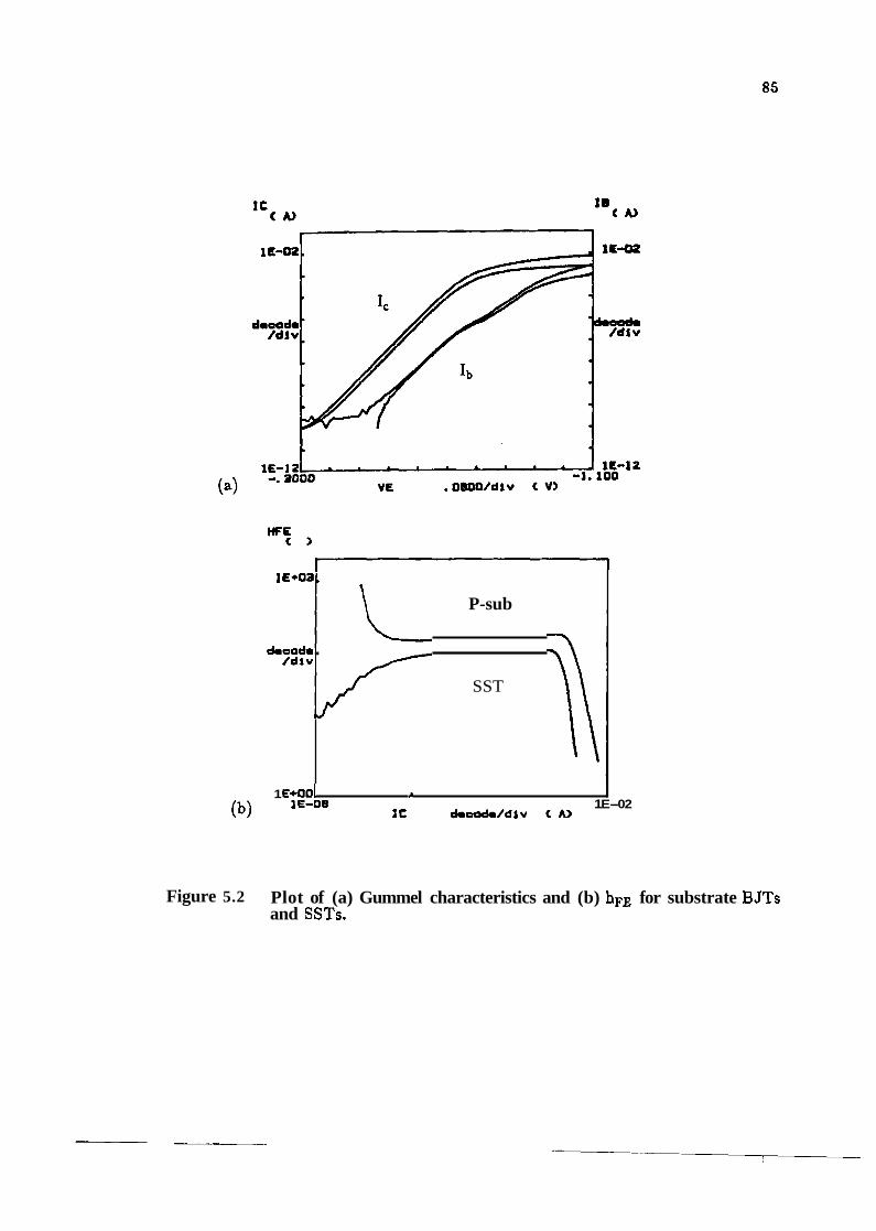
1 €*OS.
P-sub
dmoodm . l d i v
SST
1 E+OO~ I E-OB 1 E-02
IC dmaodddlv C A)
Figure 5.2 Plot of (a) Gummel characteristics and (b) hFE for substrate BJTs and SSTs.
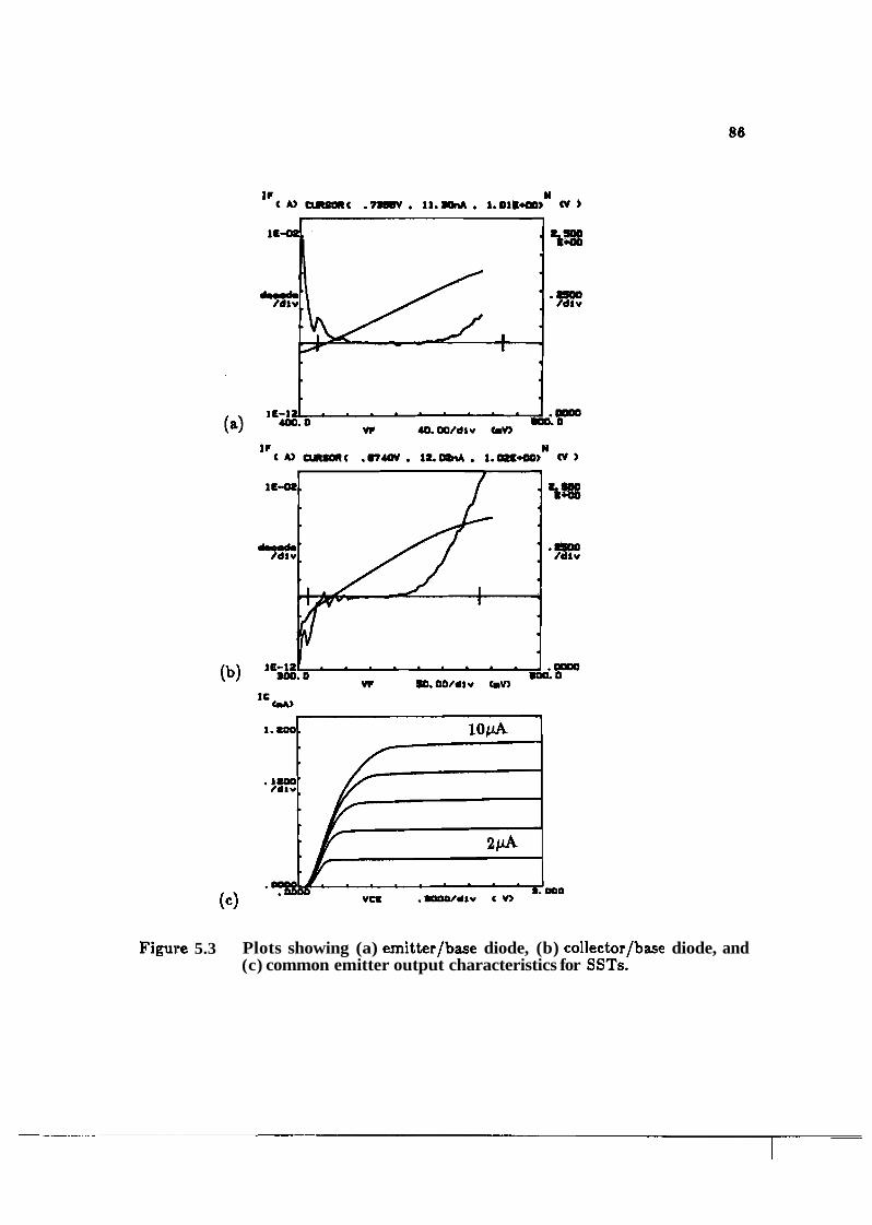
Figure 5.3 Plots showing (a) emitterlbase diode, (b) collector/base diode, and (c) common emitter output characteristics for SSTs.
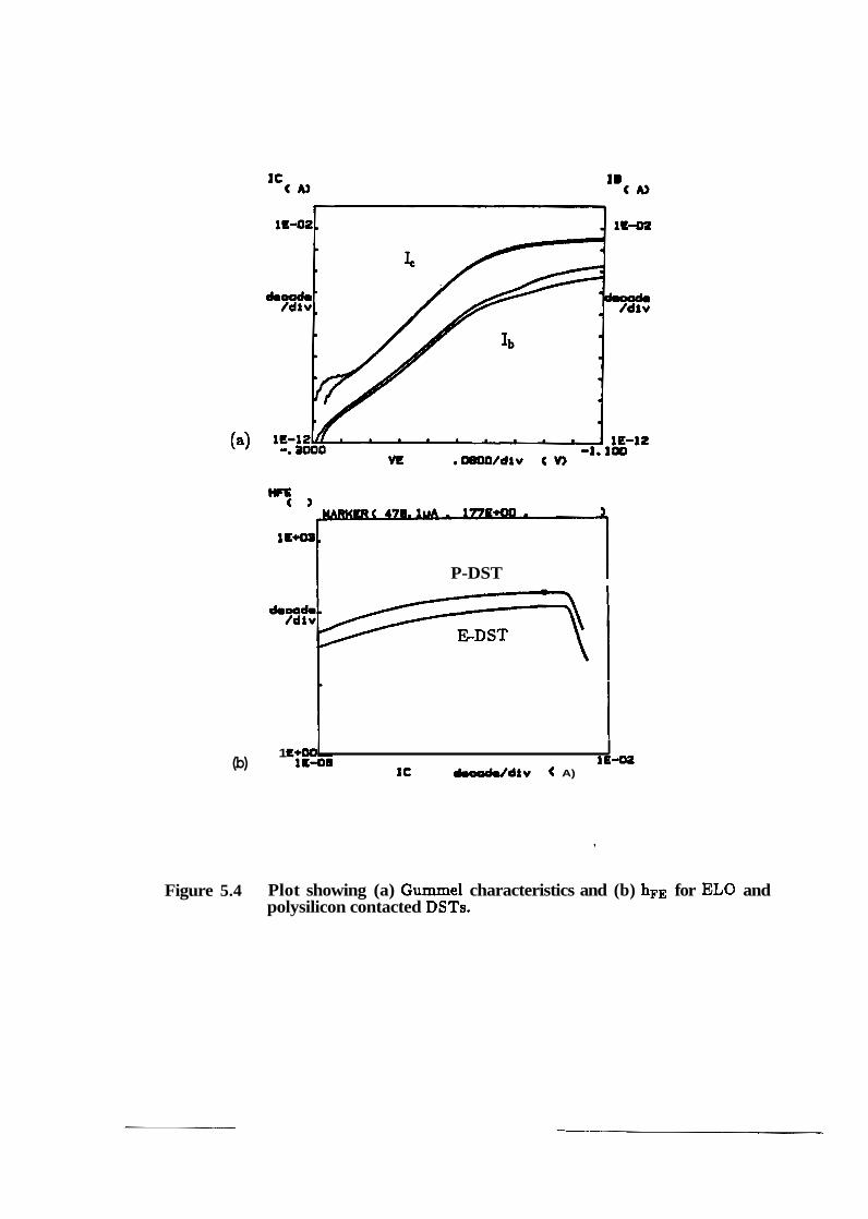
P-DST I
1 L+00 (b) 1K-b.
I 1 e-oiz
It h d d l v < A)
Figure 5.4 Plot showing (a) Gummel characteristics and (b) hpE for EL0 and polysilicon contacted DSTs.
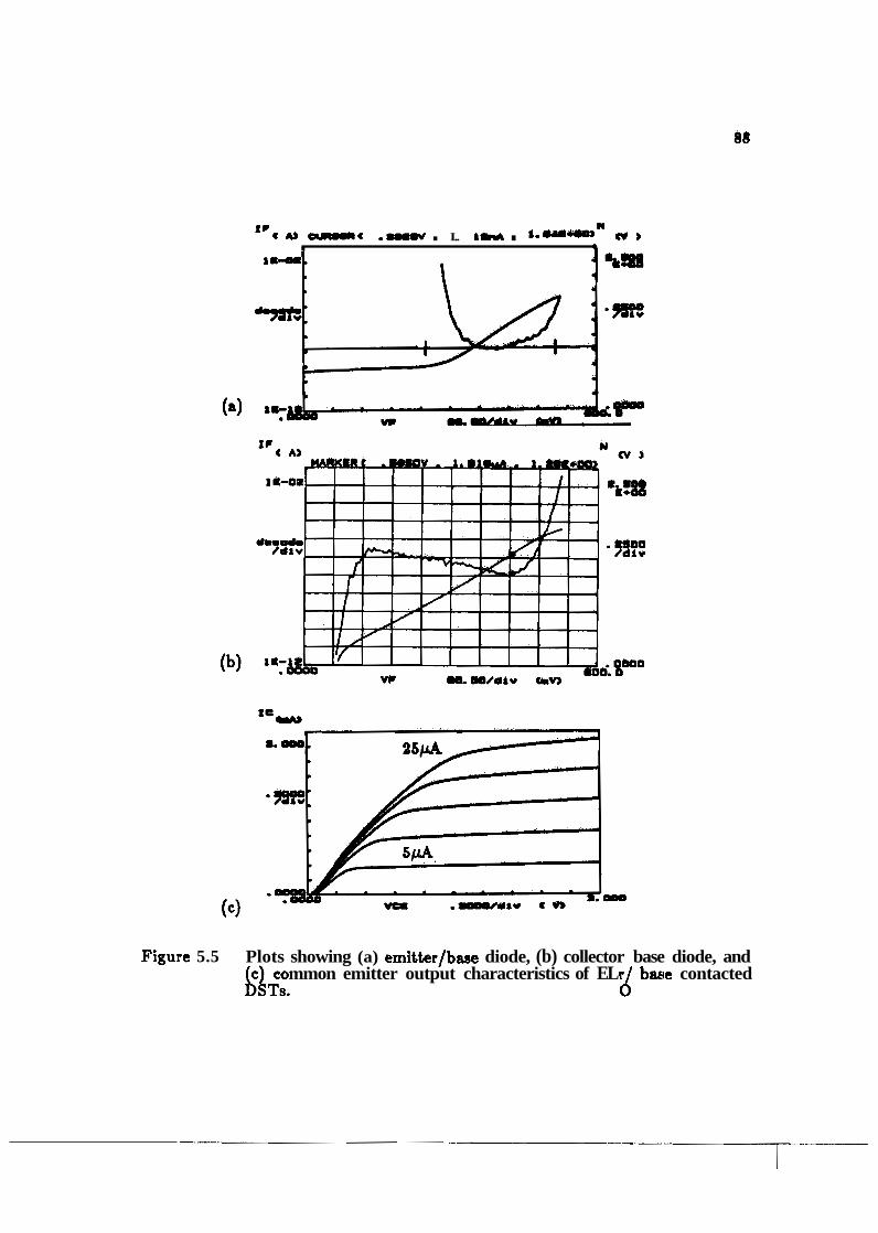
A) - a 0- . I.. I- . u s . *
Figure 5.5 Plots showing (a) emitfer/baae diode, (b) collector base diode, and c common emitter output characteristics of EL base contacted 64,. d
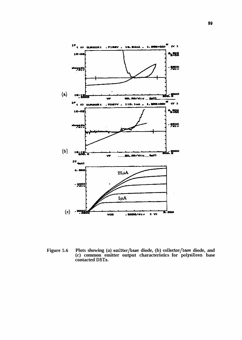
Figure 5.6 Plots showing (a) emitter/base diode, (b) collector/base diode, and (c) common emitter output characteristics for polysilicon base contacted DSTs.
for DSTs than k r SSTs, peihapi due td !edkagk ikiahgli the b&e/collictor junctions. Several EL0 base contacted DST6 dimonstiatkd qeb = i .bi and V C ~ B
= 1.04, however, thelrk devices were the exciptions d i d were not indicative of the
average devices. Clearly, device quality may be improved under certain
conditions if the process uniformity can be improved.
5.3.3 Resistor Test Structures
Electrical measurements *ere taken for ejutiinsi'c b b k resistance test
structures, and intrinsic base pinch resistdrs. For extrihsic base resistors, 10 sets of resistor bars with lengths of 10, 20, iind 3Opd %hire Seisured For contact widths between 0.2 and 0.4pm. An average of the rksulti \iidi=&kii that the ELC) bait! contacts have ribout on= half the F&lLtaxicg jiit\li-i/si$b~iiie) of the
polyailicon bak contacts (2dbfl/~QUARk) tiv& ibe i'hti & p i s and physical
dimansions. There w b very little vorioiion in kesid\&ilke $ith contact size
indicatiig that the contact bbtw&n polysiliton h d kke ~ubgtriite W& not the
major resistive iegidn fo* poljsllicon base cbnthctj h this k~nfigui%ki6n.
5.4 A.C. hlectrical datfi of BJTs
Reverse b i a capacitance datk nu meisured from 0 tb -6V tbr self-aligned
devices using an HP 4275A LCR Meter and a micromisnipulator probihg st~tion.
Figure 5.7 illustrates that Ceb consists of a junction czipacitmce (Cebj), a
dielectric capacitance {Cebd) which is due to thi overlap of the polysiliicon emitter with the extrinsic bilse contacts, and a dielkctric ckpacitrrnce (Cebm) which is due
to the overlap of the A1 emitter contact with the extrinsic barse contacts. To
eliiinhte Cebm, the emitter regions of selected devices wete etched away using an
RIE plasma leaving only the Cebm component. fn $11 cases, Cebm Was
approximately 85fF for all bias conditions f roh to -8 vblts. The rbmafning
capacitance was recorded ss Ceb and is plotted in Figure 5.8 for the snnall emitter
area devices (type 1) and in Figure 5.9 for the large area devices (type 2). As
indicirted, the SST and EDST are very similar while the P-DST is of lower
capacitance.

Cebm Cebd Cebj
p base'
n substrate / collector I I
pigure 5.7 Schematic diagram of the 3 capacitance components of Ceb for all self-aligned devices.
Basdernita voltage (V)
Figure 5.8 R e v e q bias Cob for SSTs, E-DSTs, and P-DSTs with = 2.4 x 50.4pm (type 1 device. Data is adjusted to eliminate A1 interconnect capacitance (JObm).
Baselemitter voltage (V)
Figure 5.9 Reverse bias Ceb for SSTs, E-DSTs, and P-DSTs with A, = 4.4 x ~ 4 . 4 ~ m * (type 2 . Data was adjusted .to eliminate A1 interconnect
In order to separate Cebj from Cebd, the following equation was solved for each of the self-aligned device types
Ceb(type l)=(~:~j)(junction area l)+(~:~)(dieleetric area 1)
Ceb(type 2)=(~:~~)(junction area 2)+(~h)(dielectric area 1)
where and c : ~ are the unit area values of CBb and CeM. Figure 5.10 plots the unit area junction capacitances for all self-gligned devices and indicates
reasonable agreement between the device types. It was cdculated that the unit area Cebd was different for SST, E-DST, and P-DST devices of the same area,
perh.aps due to variations in the oxide thickness between the polysilicon emitters and the base contacts. The calculated values of cibd are 0.45, 0.60, and
0.73fF/pm2 for the P-DST, E-DST, and SST devices rwpectively. Given that the
oxide over the P-DSTs was thicker than for the E-DSTs due to the faster growth
rate of polysilicon over single crystal silicon, the lower c : ~ ~ of the polysilicon
contacted devices is consistent. The difFerwce between the SST and EL0 base
contacted DST is presumably either error in the measurement or oxide thickness
variation.
PISCES-IIB simulations of Cebj and Cebd were performed by simulating only
the c:mitter/base portion of DSTs for simplicity. Figure 5.11 plots total Ceb for
E-DSTs against a PISCES-ID computer simulation of the same device structure
for both type 1 and type 2 emitter areaa. The error hetween measured and
simulated values for eero bias Cebo is a maximum of 7%. A worst case maximum
error of 33% occurs at Vb, = -1.8V. No attempt was made to alter the SUPIREM-N or PISCES simulation program to improve the fit. Error could
originate from the device measurement, the simulated junction profile, or the simulation software itself.
5.4.2 Collector/Base Capacitance
]Due to the small collector/base junction area of device types 1 and 2, a
direct measurement of Ccb was impossible given the minimum useful range of the
LCR meter. It was therefore necessary to measure large area intrinsic (Ccbi) and
extrinsic (Ccbx) collector/base capacitances by measuring CCb for the substrate
and ZSST devices respectively. By dividing the capacitance data by the junction
area, the unit area values could be used to estimate the actual CCb of self-aligned
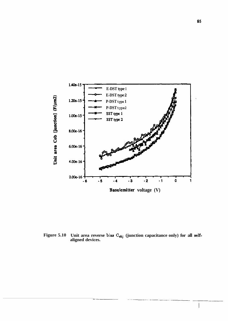
1.4Oe15 - E-DST type 1 - E-DST type 2 - P-DST type 1 - P-DST type2 - SSTtype1 - SSTtype2
Baselemitter voltage (V)
Figure 5.10 Unit area reverse bia. Cebj (junction capacitance only) for all self- aligned devices.
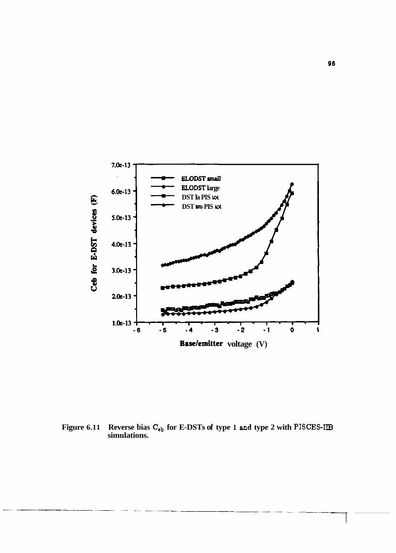
- W D S T large - DST la PIS ux - DST an PIS cot A
Baselemitter voltage (V)
Figure 6.11 Reverse bias Ceb for E-DSTs of type 1 and type 2 with PISCES-IIB simulations.
devices.
The unit area values of Ccbi and Ccbx are plotted in Figure 5.12 and 5.13
respectively along with PISCES-IIB simulations of large area capacitors. Ccbx iind Ccbi are approximately equal due to the fact that the depletion regions reside
~nostly in the lightly doped n-type collector and are therefore alniost equal. In the
case where a buried layer would be used, however, Ccbx would tend to dominate.
Figure 5.14 plots the unit area Ccb for a PISCES simulation of a full DST along
with measured values of Ccbi for type 1 and type 2 devices. The agreement is
very good over the entire 0 to -5V bias range, however, the PISCIES data seems to
jump around excessively. The PISCES simulation was performed on a DST
which contained only the collector/base junction to simplify the computation.
The DST was otherwise identical to a full device. The worst case maximum error
in Ccb occurs a t Ccbo and is always less than 18% for all device types and sizes.
!i.5 Summary
D.c. and a.c. electrical data for substrate and self-alignled devices were
ineasured for devices of different emitter areas and compared with PISCES-IIB
computer simulations. Reasonable agreement was achieved between unit area
capacitances for devices of different sizes and levels of self-alignment.
l~iscrepancies occurred between the measured and simulated values of Ceb,
perhaps due to errors in the measurement of these very low ~a~pacitance values
('100 to 7OOfF). In these cases, the stray capacitance of the probe tips to the
substrate were very difficult to null out. Collector/base capacitance was not
ineasured directly for the DSTs due to the overwhelming capacitance associated
with the probing pads and the base contact/substrate overlap capacitance.
Collector/base capacitance was therefore extracted from large area SEG base
contacted SSTs and correlated to junction area for the DSTs.
Substrate devices demonstrated lower leakage currents than self-aligned
devices and SSTs demonstrated lower collector/base leakage than DSTs. Possible
reasons for the increased leakage current include leakage in the corners of the
t?xtrinsic collector/base juction due to crystalline damage the LOCOS or due to
collector pedestal etch. P-DSTs and E-DSTs appear to have the same
performance level for most parameters. The two main exceptions were that the
1'-DSTs exhibited catastrophic failure of the emitterlbase junction through the
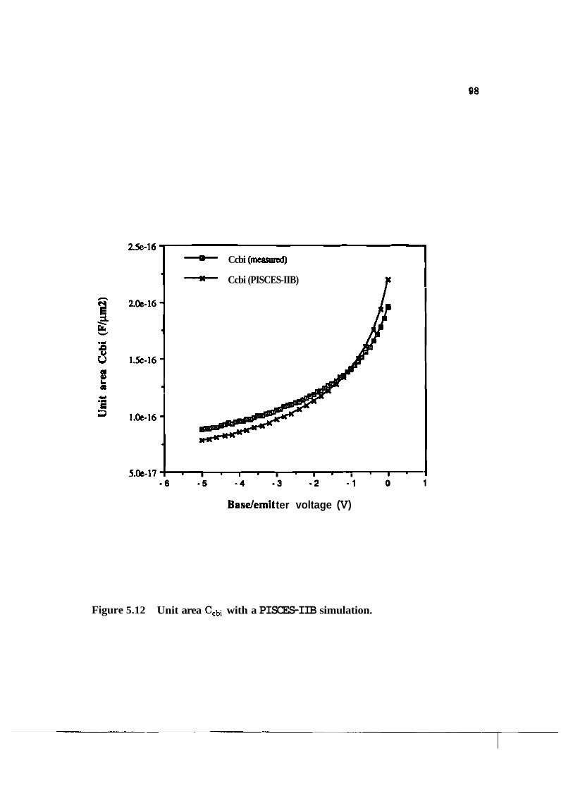
Ccbi (mawed) - Ccbi (PISCES-IIB)
-
-
-
I I . I I . I
Basdemit ter voltage (V)
Figure 5.12 Unit area Ccbi with a PISCES-IIB simulation.
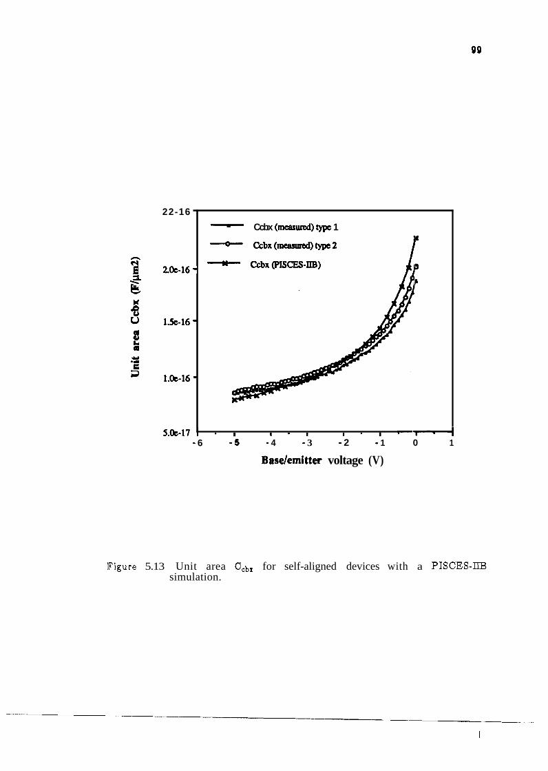
5.k-17 : I 1 . 1 I . I . M - 6 - 5 - 4 - 3 - 2 - 1 0 1
Baselemitter voltage (V)
22-16
2&16- =L - tc V
B LJ 1.2-16 - 8 L 0 Y .I ' 1.k46 -
]Figure 5.13 Unit area Ccbx for self-aligned devices with a PISCES-IIB simulation.
- Ccbx ( m e a s d ) type 1
-t Ccbx(-typt2 - C m " ( p I s ~ - ~ )
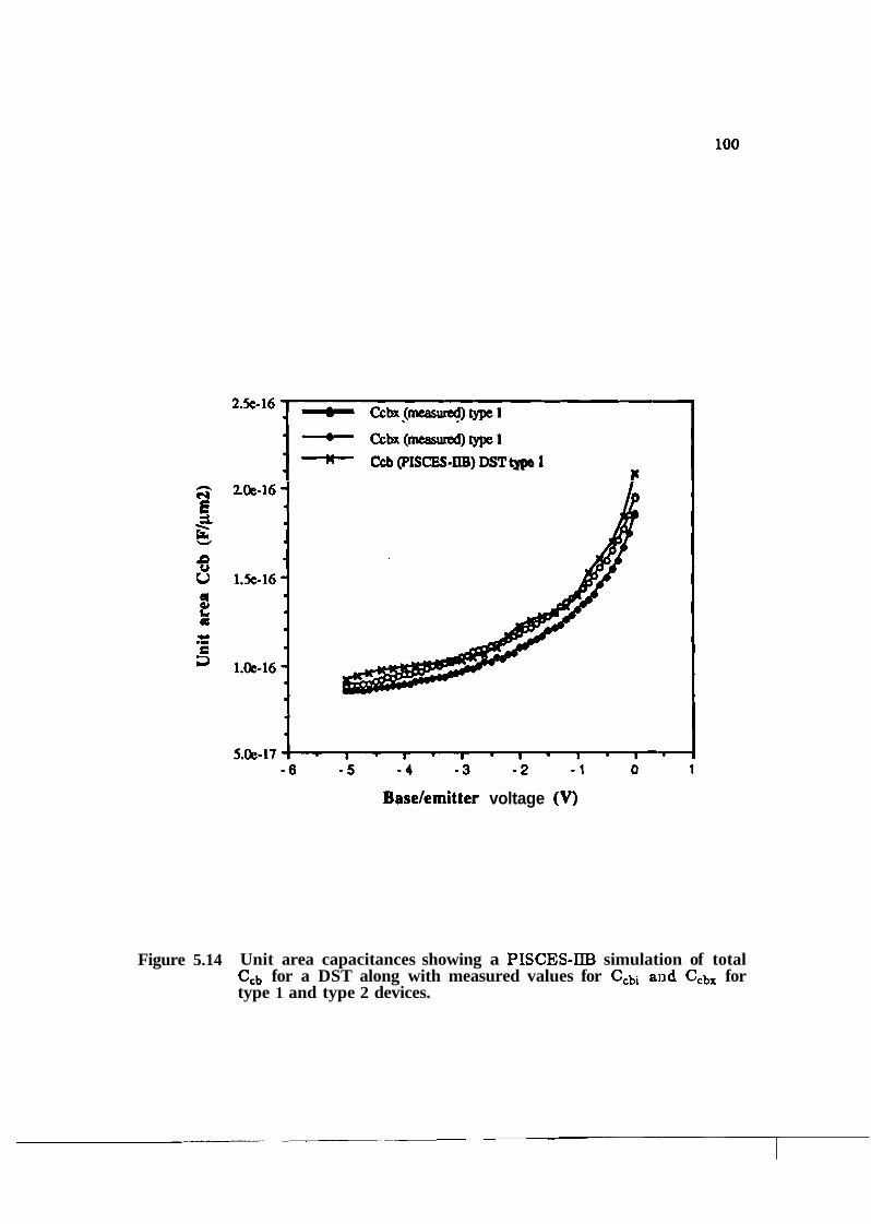
'*16 6-1 - c c b x ( r n t a S ~ t y p e 1 - Ccb (PISCES-IIB) DST type 1
Baselemitter voltage (V)
Figure 5.14 Unit area capacitances showing a PISCES-IIB simulation of total CCb for a DST along with measured values for Ccbi and Ccbx for type 1 and type 2 devices.
SSTs indicates that the self-aligned emitter is not the source of difficulty for the
DSTs. The additional processing required to fabricate the self-digned collector
pedestal for the DSTs appears to degrade the collector/base region due to the
generation of random defects. Taken on the whole, these results demonstrate the
feasibility of the DST concept using both polysilicon and EL0 single-crystal
silicon extrinsic base contacts.
CHAPTER 6
MODELING OF FULLY S C U E D HIGH-SPEED DEVICE
6.1 Overview and Purpose
Based upon the structural and electrical data extracted in chapters 4 and 6 ,
cha.pter 6 will present SUPREM-IV and PISCES-IIB computer simulations of the
fully scaled-down EL0 base contacted DST. Simulated electrical output from a
PIS'CES-IIB model of the proposed device will demonstrate the :advantage of
usi~lg double self-alignment to reduce Ccb. As discussed in chapter 3, the
proposed double self-aligned BJT utilizes two somewhat unrelated process
phi.losophies to reduce Ccb over that of a similar SST [4,10]. First, the use of self-
aligned extrinsic base contacts will eliminate the peripheral (curved) portion of
collector/base junction area along the edge of the collector pedestal. Second, the
use of single-crystal silicon base contacts will allow for reduced collector/base
junction width by scaling down the extrinsic base contact "footprint" over the
silicon pedestal. To quantify the difference in Ccb, the proposed single-crystal
contacted BJT and an identical single self-aligned transistor were simulated
together using similar intrinsic dimensions and dopant profiles as were reported
for .the SST-1A [4,10].
6.2 SUPREM-IY Process Simulations
For this work, all simulations were carried out using structures -which model
one symmetrical half of the full device to reduce simulation time. Reflecting
boundary conditions were used along the axis of symmetry. For simulation
accuracy, a high density of grid points was used around areas which .have rapidly
changing dopant profiles. Due to limitations on the maximum number of grid
points which may be employed, oxidation of the collector pedestal was modeled
using a separate grid profile to maximize the grid density for simulation accuracy.
After the final collector oxidation profile was obtained, a simplified re:presentation
of the oxide profile was used for simulation of the full device.
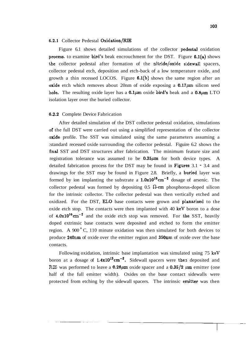
ti.2.1 Collector Pedestal Oxidation/RE
Figure 6.1 shows detailed simulations of the collector petlestal oxidation
]>recess. to examine bird's beak encrouchment for the DST. Figure 6.l(a) shows
the collector pedestal after formation of the nitride/oxide sidewall spacers,
collector pedestal etch, deposition and etch-back of a low temperature oxide, and
growth a thin recessed LOCOS. Figure 6.l(b) shows the same region after an
oxide etch which removes about 20nm of oxide exposing a 0.17pm silicon seed
liole. The resulting oxide layer has a O.1pm oxide bird's beak and a 0.8pm LTO
isolation layer over the buried collector.
8.2.2 Complete Device Fabrication
After detailed simulation of the DST collector pedestal oxidation, simulations
of the full DST were carried out using a simplified representation of the collector
oxide profile. The SST was simulated using the same parameters assuming a
:standard recessed oxide surrounding the collector pedestal. Figuire 6.2 shows the
:final SST and DST structures after fabrication. The minimum feature size and
registration tolerance was assumed to be 0.35pm for both device types. A
detailed fabrication process for the DST may be found in Figur'es 3.1 - 3.4 and
drawings for the SST may be found in Figure 2.8. Briefly, a buried layer was
formed by ion implanting the substrate a 1 . 0 ~ 1 0 ~ ~ c m - ~ dosage of arsenic. The
collector pedestal was formed by depositing 0.5 a c m phosphorus-doped silicon
for the intrinsic collector. The collector pedestal was then vertically etched and
oxidized. For the DST, EL0 base contacts were grown and pl.anarized to the
oxide etch stop. The contacts were then implanted with 40 keV boron to a dose
of 4 .0x10~~cm-~ and the oxide etch stop was removed. For the SST, heavily
doped extrinsic base contacts were deposited and etched to form the emitter
region. A 900 C, 110 minute oxidation was then simulated for both devices to
produce 240nm of oxide over the emitter region and 350nm of oxide over the base
contacts.
Following oxidation, intrinsic base implantation was simulated using 75 keV
boron a t a dosage of 1.4~10'~crn-~. Sidewall spacers were thein deposited and
RIE was performed to leave a 0.26pm oxide spacer and a 0.35/2 pm emitter (one
half of the full emitter width). Oxides on the base contact sidewalls were
protected from etching by the sidewall spacers. The intrinsic e:mitter was then
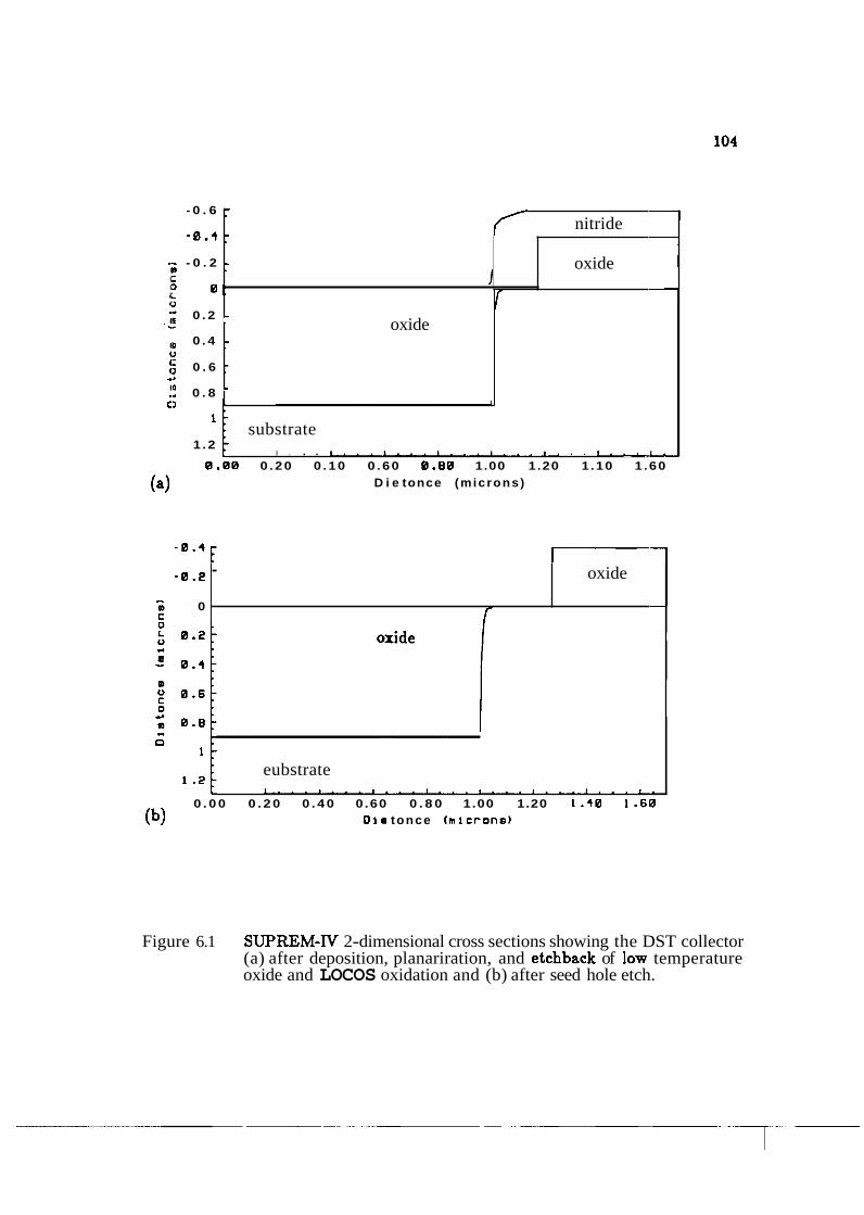
1 substrate
1 .2 I . . . k . . . l . . . I . . . I . . . I . . . I . . . h
- 0 . 6
- 0 . 1
- 0 . 2
0 ,
0 . 2
0 . 4
0 . 6
0 . 8
0 . 0 0 0 .20 0 .10 0 .60 0 .00 1.00 1.20 1 .10 1 .60 D i e tonce (microns)
- nitride
- - -
eubstrate l . . . . l . . . I . . . I . . . I . . . I . . . I . . . I L
0 . 0 0 0 . 2 0 0 . 4 0 0 .60 0 . 8 0 1.00 1.20 1.40 1 .60 Ole tonce (microns)
: 1
- 0 . 2
0
Figure 6.1 SUPREM-IV 2-dimensional cross sections showing the DST collector (a) after deposition, planariration, and etchback of low temperature oxide and LOCOS oxidation and (b) after seed hole etch.
-
oxide
I -
: oxide :
-
- oxide
r -
base em l tter
C I '
0.25 1 p+ EL0 or polyslllcon base contact
5 0.501 Y oxlde
n- lntrlnslc collector
- z I -----,-.I--- w 1.25
collector . n+ burled colllector 1 base em l t ter
n
0*25t p+ polyslllcon base contact 1
oxlde P +
I.- - 7---.-.-
n- lntrlnslc collector I
> a . 2 5 1-j
. - w - w - - - - - - - - - - - - - - - - -
collector n+ burled collect.or
devlce w ldth (pm) 0.17pm
Figure 8.2 SWREM-IV cross sections showing (a) the proposed double self- aligned BJT (DST), and (b) the comparison SS'I.' structure after final processing.
forined by depositing heavily arsenic doped silicon over the enlitter opening
foll~owed by a rapid thermal anneal at 1000' C in nitrogen for 1.5 minutes to drive the emitter. Finally, contact holes were etched and aluminum was
deposited. A close-up view of the intrinsic device region for the DST is shown in
Figure 6.3 to illustrate the final mesh.
One-dimensional cross sections taken through the intrinsic
emitter/base/collector/buried collector and through the extrinsic base
contact/collector/buried collector for both SST and DST are shown in Figure
6.4(aJb). The plots are given using the same scale. The vertical profile indicates
that the polysilicon emitter, single-crystal emitter, and base are 340, 60, 160nm
thick respectively for both SST and DST. The extrinsic base region:; are virtually
identical for SST and DST as indicated in the figure.
6.3 PISCES-IIB - Electrical Process Emulator
The purpose of this section is to predict the electrical behavior of the
proposed device. As these are twa-dimensional simulations, all parameters have
been multiplied by the perimeter length of the device to achieve dimensionless
parismeters. To examine the potential advantages of the proposed DST, a side-
by-side comparison with the simulated SST will be presented along with reported
pariimeters for the SST-1A [4,10].
6.3.l DC Characteristics
A Gummel plot with both SST and DST is shown in Figure 6.5(a). A
corresponding plot of hFE versus 1, is given in Figure 6.5(b). The SST and DST
are :not distinguishable on the Gummel plot but a slight difference may be seen on
the hFE plot. This difference in hFE is due to a slight variation in the
encroachment of the extrinsic base around the emitter between the two devices.
hFE--mar is about 34 for both devices. The low value of hFE-max is a, direct result
of the fact that PISCES does not currently simulate the physical phenomenon
associated with true polysilicon emitters such ae interfacial oxide layers and
partial recrystallieation. As a result, the reduction in back injected hole current
which occurs for real polysilicon emitters is not simulated and the emitter
injection efficiency is therefore artificially low. For a real polysilicon emitter, one
may expect an hFE enhancement of greater than 3 in nearly all cases, thus a value
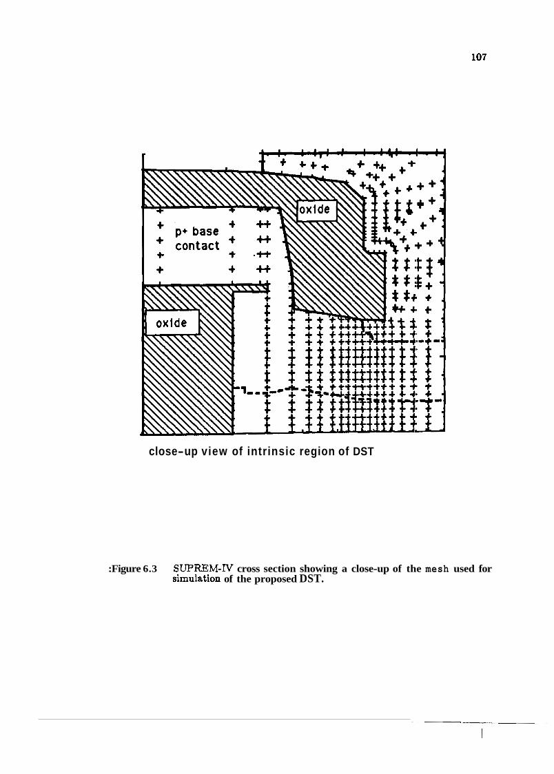
close-up view of intrinsic region of DST
:Figure 6.3 SUPREM-N cross section showing a close-up of the mesh used for simulation of the proposed DST.
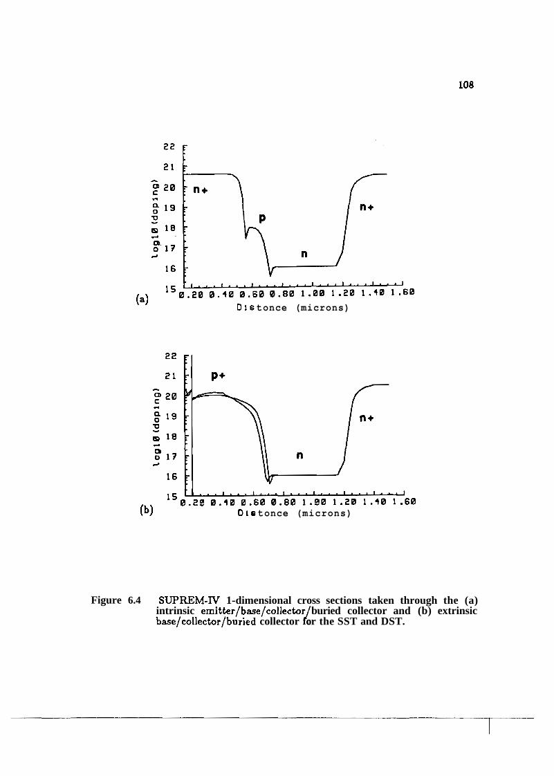
(a) D i s tonce (microns)
(b) 131s tonce (microns)
Figure 6.4 SWREM-IV 1-dimensional cross sections taken through the (a) intrinsic emitter/base/collector buried collector and (b) extrinsic base/collector/buried collector / or the SST and DST.
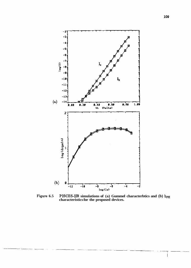
Vb. (Volf.)
I'igure 6.5 PISCES-IIB simulations of (a) Gummel characterbtics and (b) hFe characteristics for the proposed devices.
of 34 would scale to at least 100 which is satisfactory for ldigital circuit
ap;plications. For these simulations, PISCES was programmed to account for
field-dependent mobility, concentration-dependent mobility, band-gap narrowing,
and concentration-dependent SRH, To extract rb,, contours displaying thc quasi-
Fermi level potential for holes were plotted for Vb, of 0.8 V. The extrinsic base
resistance was defined as the difference between the potential at the base terminal
and the potential a t the edge of the emitter region divided by the base current, A
contour plot is given in Figure 6.6 for the DST. The potential difference between
the base electrode (0.8V) and the potential contour at the edge o'f the emitter
(0.7997V) is 300pV for a base current of 430nAIpm. Thus, rbx-pm == 30010.43 =
698'npm. To estimate the total rbx, we include the influence of emilbter length on
both sides (5pm) plus the contribution from both ends of the emitter (2 x 0.35pm)
giviing rb, -- 698apm / 10.7pm cz 65R. The same is true for the simulated SST
within the.leve1 of accuracy of this technique. This number is artificially low due
to the absence of metal line sheet resistance, metal contact resistance, and
po~vsilicon/silicon interfacial contact resistance in the case of the SST. For the
SST-lA, a total base resistance of 310 is reported with no separation into
intrinsic and extrinsic components. However, experimental and theoretical
reports concerning self-aligned BJTs, indicate that a typical rb, fo'r an emitter
length of 5pm would be somewhere in the range of 19 to 67 a [6,103].
6.3.2 AC Characteristics
To simplify the extraction Cbe and Ccb, the device structure wag modified to
include only the junctions being probed. Figure 6.7(a) and (b) show the
simplified structures for measurement of Cb, and Cb, respectively ibr the DST.
For the emitterlbase test structure, the n-type collector and buried layer were
replaced with low doped p-type silicon to exclude junction effects. For this case,
the collector terminal was not included in the electrical analysis. The zero bias
capz~citance was measured using a 15mV, lOOkHz a.c. signal on the base terminal.
Similarly, the collector/base test structure of Figure 6.7(b) was created by
excluding all emitter implant and etch sequences. In both cases, the test
structures were otherwise identical to the full structure.
Both the proposed BJT and the SST have virtually identical siinulated Cbe
at 7.4 fF This figure compares with a reported value of 10.4fF for the SST-1A
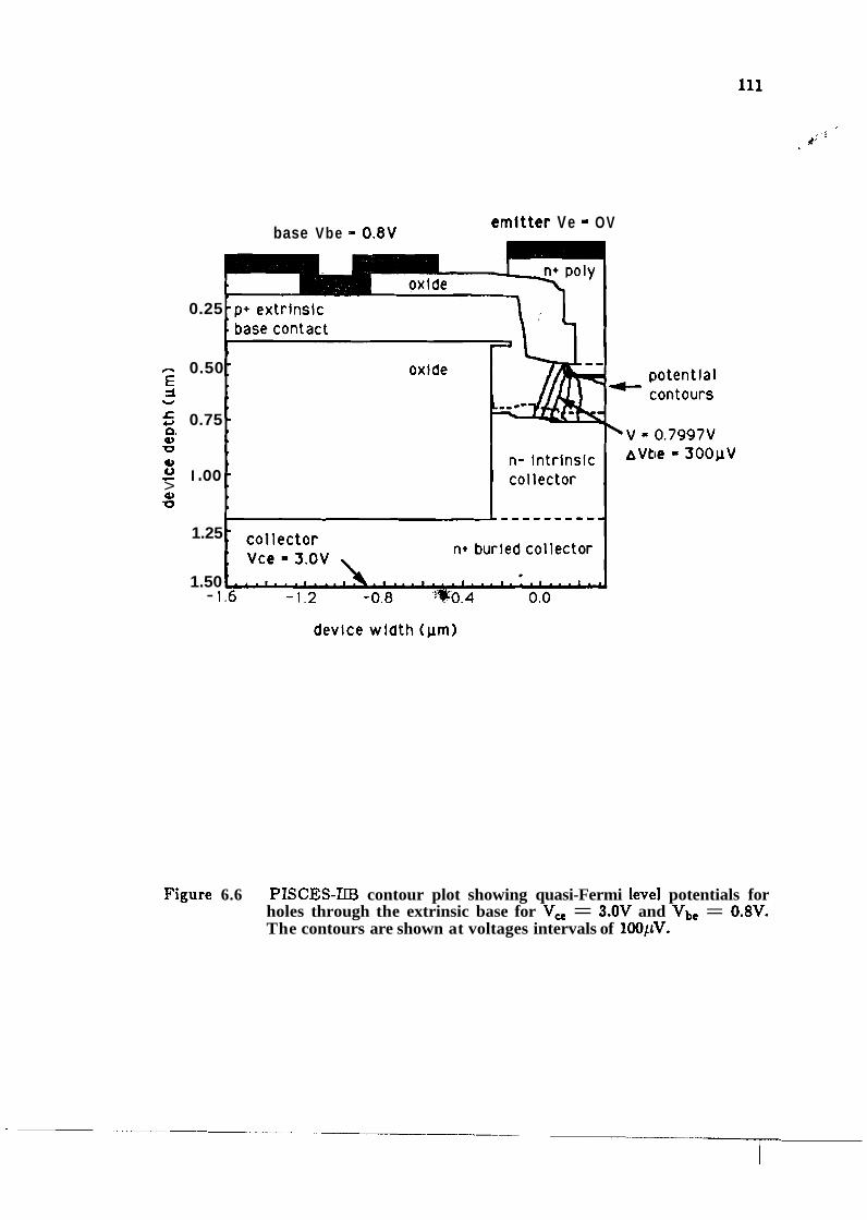
base Vbe = 0.8V emftter Ve - OV
0.25
- 0.50 E 5 V
5 0.75 0. Q, -0 0
aVbe - 300pV 2 I .oo > Q, -0
1.25
1.50 - 1
Figure 6.6 PISCES-IIB contour plot showing quasi-Fermi levlel potentials for holes through the extrinsic base for V, = 3.OV and Vb, = 0.8V. The contours are shown at voltages intervals of 100pV.
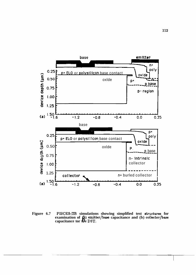
base emitter
f i Oe2'[ p+ EL0 or polys l l icon base contact c i \ 0 x l d ~ 1 1 I
oxlde
base
I col lector I
n
0.25
E 3 0.50 Y
5 a 0.75 4) u
f p+ EL0 or po lys l l Icon base contact .-
: oxlde \ O x l d t k ~ ~ ~
P + p base L-------- -.----- : . n- In t r lns lc
Figure 6.7 PISCES-IIB simulations showing simplified test stiructures for examination of a) emitter/base capacitance and (b) collector/base capacitance tor t 6 e DST.
% u 1.25
I - - - - - - - - o - - -
: ~ 0 l l e ~ t 0 r . n+ burled col lector I
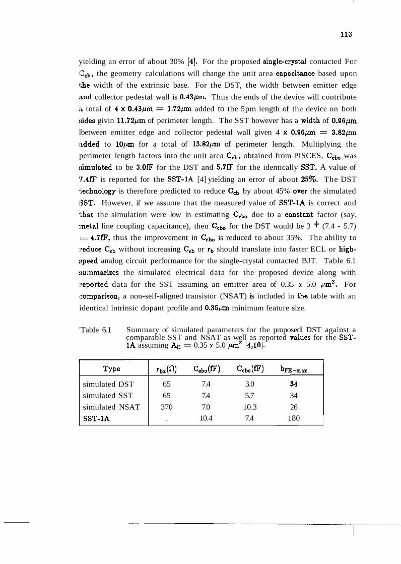
yielding an error of about 30% [4]. For the proposed single-cryst;sl contacted For
Ccb, the geometry calculations will change the unit area capacitirnce based upon
the width of the extrinsic base. For the DST, the width between emitter edge
and collector pedestal wall is 0.43pm. Thus the ends of the device will contribute
:% total of 4 x 0.43pm = 1.72pm added to the 5pm length of the device on both
sides givin 11.72pm of perimeter length. The SST however has a .width of 0.96pm
lbetween emitter edge and collector pedestal wall given 4 x 0.916pm = 3.82pm
added to lOpm for a total of 13.82pm of perimeter length. Multiplying the
perimeter length factors into the unit area Ccbo obtained from PISCES, Ccbo was
:jimulated to be 3.0fF for the DST and 5.7fF for the identically ISST. A value of
'7.4fF is reported for the SST-1A [4] yielding an error of about :25%. The DST
ltechnology is therefore predicted to reduce Ccb by about 45% over the simulated
ISST. However, if we assume that the measured value of SST-1A is correct and
that the simulation were low in estimating Cch due to a const'ant factor (say,
imetal line coupling capacitance), then Ccbo for the DST would be 3 + (7.4 - 5.7)
:= 4.7fF, thus the improvement in Ccbo is reduced to about 35%. The ability to
ireduce Ccb without increasing Ceb or rb should translate into faster ECL or high-
!jpeed analog circuit performance for the single-crystal contacted BJT. Table 6.1
!~ummarizes the simulated electrical data for the proposed device along with
reported data for the SST assuming an emitter area of 0.35 x: 5.0 pm2. For
comparison, a non-self-aligned transistor (NSAT) is included in the table with an
identical intrinsic dopant profile and 0.35pm minimum feature size.
'Table 6.1 Summary of simulated parameters for the proposedl DST against a comparable SST and NSAT as well as reported val~ies for the SST- 1A assuming AE = 0.35 x 5.0 pm2 [4,10].
Type
simulated DST
simulated SST
simulated NSAT
SST-1A
rbx (St) Cebo (fF) Ccbo (fF) h ~ ~ - m a x
65 7.4 3.0
65 7.4 5.7 34
370 7.0 10.3 26
- 10.4 7.4 180
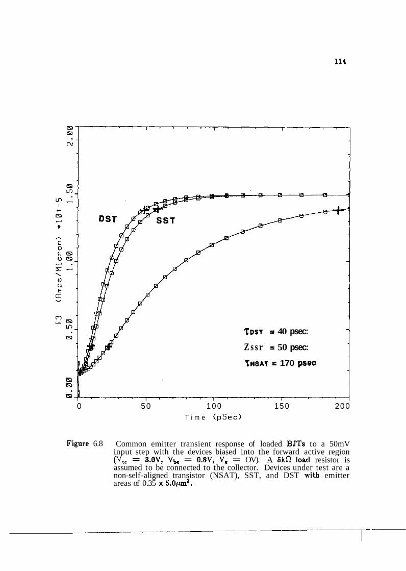
-
ZDST = 40 psec: -
Z s s r = 50 psec:
ZNSAT = 170 psec
0 50 1 0 0 1 5 0 200 T i m e (pSec>
Figure 6.8 Common emitter transient response of loaded BJTs to a 50mV input step with the devices biased into the forward active region (V, = 3.OV, Vb, = 0.8V, V, = OV). A 5kn loacl resistor is assumed to be connected to the collector. Devices under test are a non-self-aligned transistor (NSAT), SST, and DST with emitter areas of 0.35 x 5.0pm2.
Finally, the device technologies are compared in a circuit application to
measure the influence of loading conditions. For this comparison, the NSAT,
$;ST, and DST were biased to 0, 0.75, and 3.OV on the emitter, base, and collector
respectively with a lumped 5kR collector load resistance added. The common
emitter base input was then pulsed to 0.8V (50mV step) and the response of the
c:ollector current was observed as plotted in Figure 6.8. Response time was
clefined as the time required to change state from 10% to 90% of the final
c;ollector current. As indicated, a 70% decrease in response time is achieved when
going from NSAT to SST due to the reduction of CCb anld rb,. A 20%
improvement is achieved when going from SST to DST despite the 45% reduction
of Ccb. The limit to improvement in transient response may be due to the
limitation of other delay factors, such as base transit time, which fundamentally
limit the response of the device.
6.4 Summary
The simulations chosen for this chapter were intended to illustrate the
potential for scaling down collector/base junction area without degrading base
~besistance. The exact dimensions used for the preceding simulations were meant
l,o represent a limiting case of high integration and reduced lateral width. For
t!xample, the choice of a 0.17pm EL0 base contact seed hole may need to be
enlarged to stablize process variation. Overall, the simulations were intended to
examine the basic functionality of the device design in an attempt to spot
significant problems or non-idealities. The simulations were also helpful as a
learning tool by illustrating the impact of process variation on operating
conditions.
For single-self-aligned BJTs, the limits to scaling emitte,r width, spacer
width, and base contact width necessitate the decrease in overall device length to
ischieve reduced the area-dependence of Ccb. Unfortunately, the reduction of
emitter length will increase base resistance and the overall reduction in emitter
isrea will increase collector current densities resulting in premature high-level
injection. As an alternative, the proposed device offers to reduce Ccb through
:self-alignment of the base contacts to the collector pedestal and scale-down of the
base contact footprint.
CHAPTER 7
CONCLUSIONS
7.1 Summary
During the development of this project, a fully self-aligned high-speed npn
bipolar transistor using single crystal silicon base contacts was first simulated
using SWREM-IV and PISCES-IIB software to estimate the potential advantages
over single self-aligned polysilicon base contacted devices. Second, a set of
contact photomasks was developed to examine the self-aligned emitter and self-
aligned base regions of a scaled-up version of the proposed structure in order to
fabricate test devices. Third, non-self-aligned and single self-aligned transistors
were fabricated and characterized in order to generate a viable fabrication process
Forth, fully self-aligned bipolar transistors with both E L 0 single crystal silicon
and LPCVD deposited polysilicon base contacts were fabricated and
characterized. Finally, SUPREM-VI and PISCES-IIB simulations were correlated
with measured data from self-aligned transistors and the fully scaled high-speed
double self-aligned transistor was redesigned and resimulated using the input
gained from the research to date.
Non-self-aligned, single self-aligned, and double self-aligned trainsistors with
polysilicon contacted emitters were measured to have hFE-max between 100 and
170. Junction ideality was excellent for single self-aligned devices while double
self-aligned devices showed degraded collector/base junction performance.
Collector/base junctions showed increased reverse bias leakage wh.ich did not
scale with junction area or perimeter length. The leakage may be caused by the
extended processing required to produce the double self-aligned base contacts or
due to defects in the outside corners of the extrinsic base contacts. Single-crystal
silicon and polysilicon base contacted double self-aligned devices showed similar
characteristics, except that polysilicon base contact resistance was found to be
about twice as large as for single crystal silicon base contacts and polyoxides were
fount1 to breakdown a t lower voltages than SiOz grown from single-crystal silicon.
PISCES-IIB and SUPREM-IV computer simulation were found to correlate
r'easonably well with electrical and structural data for self-aligned transistors.
Unit area junction capacitances for different device sizes c~rrelat~ed within a few
percent within each device type and correlated within less than about 4095, for
t.he worst case, between single self-aligned and double self-alignled device types.
Worst case correlations between PISCES-IIB simulations and measured data were
within a maximum of 18% for collector/base unit area capacitances and within
about 33% for emitterlbase junction capacitances. Overall, these results both
d.emonstrate the feasibility of the proposed double self-aligned device structure
a.nd validate the use of the simulation tools in estimating device parameters for a
scaled-down version of the fabricated device. PISCES-IIB simulat,ions of the fully
scaled double self-aligned device indicate that the collector/base capacitance
should be reduced by about 45% over a comparable single self-aligned device
while response in a circuit may not yield such a dramatic improvement due to
other fundamental limitations.
7.2 Future Research
The most pressing issue to pursue in finalizing this studly would be to
i:nvestigate and correct the collector/base junction nonideality. The vertical
reactive ion etch or the LOCOS oxidation processes may need to be refined. The
silicon nitride layer used for the LOCOS oxidation may need to be replaced with
a, thin nitride layer under a deposited oxide as proposed for the fully scaled
dlevice. The differences between PISCES simulations and measured emitterlbase
capacitance need to be corrected without simply fitting the simula.tion to the data
a.rbitrarily. Any fit should work for different device sizes.
A fully scaled device might be fabricated using the electron beam system. In
this case, a special pad configuration must be used in order to probe the devices
for fT using a network analyeer. I suggest consulting the IC Design Center at
Ilelco Electronics for a suitable layout which would then fit into their test fixture.
If the layout is not proper, an accurate fT measurement cannot be obtained
regardless of the test fixture or measurement system. In the case of a fully scaled
dlevice, a thick deposited field oxide should also be used before metal deposition to i~nsulate all electrodes. A true polysilicon emitter must also be used in place of a
polysilicon contacted emitter to reduce the emitter depth.

LIST OF REFERENCES
LIST OF REFERENCES
1. G. Zorpette, "Minis and Mainframes," IEEE Spectrum, January, pp. 30 (1990).
2. B. Santo and K. T. Chen, "Solid State," IEEE Spectrum, January pp. 41 (1990).
T. Sakai, Y. Kobayashi, H. Yamauchi, M. Sato and T. Makino,, "High Speed Bipolar ICs Using Super Self-Aligned Process Technology," ,lpn. J. Appl. Phys., v. 20 Supplement 20-1, pp. 155 (1981).
S. Konaka, Y. Yamamoto and T. Sakai, "A 30-ps Si Bipolar IC] Using Super Self-Aligned Process Technology," IEEE Trans. Elect. Deu., ED-11, no. 4, pp. 526 (1986).
J.M.C. Stork, "E3ipolar Transistor Scaling for Minimum Switching Delay and Energy Dissipation," Proceedings o f the 1988 International Electron Devices Meeting, pp. 55, 1988.
E-F Chor, A. Brunnschweiler and P. Ashburn, "A Propisgation-Delay Expression and its Application to the Optimization of Polysil.icon Emitter ECL Processes," IEEE J. Solid State Circuits, v. 23, no. 1, pp. 2'51 (1988).
Y. Yamamoto and K. Sakuma, "SDX: A Novel Self-Aligned Technique and its Application to High-Speed Bipolar LSI1s," IEEE Trans. Elect. Deu. v. 35, no. 10, pp. 1601 (1988).
J. van der Velden, R. Dekker, R. van Es, S. Jansen, M. Koolen, P. Kranen, H. Maas and A. Pruijmboom, %ASIC: An Advanced High--Performance Bipolar Process," Proceedings of the 1989 International Electron Devices Meeting, pp. 233, December 1989.
H. Goto, "J?uture Bipolar Device Structures," Journal de Physique, Colloque C4, Supplement 9, pp. 471 (1988).
S. Konaka, E. Yamamoto, K. Sakuma, Y. Amemiya and T. Salkai, "A 20-ps Si Bipolar IC Using Advanced Super Self-Aligned Process Teclhnology with Collector Ion Implantation," IEEE Trans. Elect. Deu. v. 36, no. 7, pp. 1370 (1989).
P-F. Lu, 'Low-Temperature Avalanche Multiplication in the Collector-Base Junction of Advanced n-p-n Transistors," IEEE Trans. Elect. Deu. v. 37, no. 3, pp. 762 (1990).
P-F. Lu, J.H. Comfort, D.D. Tang, B.S. Meyerson, and J.Y.-C. Sun, "The Implementation of a Reduced-Field Profile Design for High-Performance Bipolar Transistors," IEEE Trans. Elect. Deu. v. 11, no. 8, pp. 3:36 (1990).
13. J.A. Del Alamo and R.M. Swanson, "Forward-Bias Tunneling: A Limitation to Bipolar Device Scaling," IEEE Electron Dev. Let. EDL7, no. 11, pp. 629 (1986).
1.4. S.-L. Zhang, M. Harnrnar, T. Johansson, and R. Buchta, 'Properties of WSiz : Ohmic contact to n+ and p+ Si, Barrier Between A1 and Sil, and Feasibility as First Metal in Multilevel Metalization Process", Journ,al de Physique, Colloque C4, Supplement 9, pp. 171 (1988).
1.5. J.A. Friedrich and G.W. Neudeck, 'Interface Characterization of Silicon Epitaxial Lateral Growth over Existing SiOz for Three-Dimensional CMOS Structures," IEEE Electron Dev. Let. EDL10, no. 4, pp. 144 (1989).
1.6. A. Ishitani, H. Kitajima, K. Tanno and H. Tsuya, "Selective Silicon Epitaxial Growth for Device-Isolation Technology," Microelectronics Engineering v. 4, pp. 3 (1986).
1,7. N. Endo, K. Tanno, Y. Kurogi and H. Tsuya, "Novel Device Isolation Technology with Selective Epitaxial Growth," IEEE Trans. Elect. Dev. ED- 31, no. 9, pp. 1283 (1984).
118. J.O. Borland, "Novel Device Structures by Selective Epitaxial Growth (SEG)," Proceedings of the 1987 International Electron Devices Meeting, pp. 12, December 1987.
119. G.W. Neudeck, "A New Epitaxial Lateral Overgrowth Silicon Bipolar Transistor," IEEE Electron Dev. Let., EDL-8, no. 10 (1987).
20. J.N. Burghartz, J.H. Comfort, G.L. Patton, B.S. Meyersoln, J.Y.-C. Sun, J.M.C. Stork, S.R. Mader, C.L. Stanis, G.J. Scilla and B.J. Ginsberg, "Self- Aligned SiGe-Base Heterojunction Bipolar Transistor by Selective Epitaxy Emitter Window (SEEW) Technology," IEEE Electron Dev. Let., v. 11, no. 7, pp. 288 (1990).
21. J.L. Glenn, Jr. and G.W. Neudeck, 'Nigh-Speed Fully SelflAligned Single- Crystal Contacted Silicon Bipolar Transistor," Electron. Let., v. 26, no. 20, pp. 1677 (1990).
22. P.V. Gilbert, J.L. Glenn, Jr., G.W. Neudeck and J.P. llenton, "Silicon Selective Epitaxy BJTs: Quasi-Dielectrically Isolated and Self-Aligned Single-Crystal Contacted," Proceedings of TECHON 90, pp. 81, October 1990.
23. J. Haisma, "SO1 Technologies: Their Past, Present, and Fnture," European Solid State Device Research Conference Proceedings, C4-3 - C4-9, Montpellier, France, September 1988.
24. S.M. Fisher, M.L. Hammond and N.P. Sandler, 'Reduced Pressure Epitaxy in an Inductively-Heated Vertical Reactor," Solid State TecAmology, pp. 107, January (1986).
25. L. Jastrebski, J.F. Corboy and R. Soydan, "Issues and Probllems Involved in Selective Epitaxial growth of Silicon for SO1 Fabrication," J. Electrochem Soc. v. 136, no. 11, pp. 3606 (1989).
B. Davari, C.W. Koburger, R. Scultz, J.D. Warnock, T. Furukawa, et al., "A New Planarization Techniyye, Using a Combination of RIE and Chemical Mechanical Polish (CMP), Proceedings of the 1989 Interno:tion Electron Devices Meeting, pp. 61, December 1989. G. Shahidi, et. al., "Fabrication of CMOS on Ultrathin SO1 Obtained by Epitaxial Lateral Overgrowth and Chemical-Mechanical, Polishinge, Proceedings of the IEDM, paper 25.2.1, 1990.
P.J. Schubert and G.W. Neudeck, "Confined Lateral Selective Epitaxial Growth of Silicon for Device Fabrication," IEEE Electron Dev. Let., v. 11, no. 5, pp. 181 (1990).
P.J. Schubert and G.W. Neudeck, "Vertical Bipolar Transistors Fabricated in Local Silicon on Insulator Films Prepared Using Confined Lateral Selective Epitaxial Growth (CLSEG)", IEEE Trans. Elect. Dev., v. 37, no. 11, pp. 2336 (1990).
J. Bloem and W.A.P. Claassen, "Rate-Determining Reactions and Surface Species in CVD of Silicon I. The SiH4-HCI-H2 System", J. Crystal Growth, v. 49, pp. 435 (1980).
W.A.P. Claassen and J. Bloem, 'Rate-Determining Reactions and Surface Species in CVD of Silicon 11. The SiH2C12-H2-N2HC1 System", J. Crystal Growth, v. 50, pp. 807 (1980).
F.W. Smith and G. Ghidini, "Reaction of Oxygen with Si(ll1) and (100): Critical Conditions for the Growth of Si02", J. Electrochem. Soc., v. 129, no. 6, pp. 1300 (1982).
G. Ghidini and F.W. Smith, 'hteraction of H 2 0 with Si(l1l) and (100): Critical Conditions for the growth of Si02", J. Electrochem Soc., v. 131, no. 12, pp. 2924 (1984).
G.W. Cullen and F.J. Corboy, J. Crystal Growth, v. 70, pp. 230 (1984).
G.R. Srinivasan and B.S. Meyerson, "Current Status of Reduced Temperature Silicon Epitaxy by Chemical Vapor DepositionM, J. Electrochem. Soc.:Solid-State Science and Technology, v. 134, no. 6, pp. 1518 (1987). J. Friedrich and G.W. Neudeck, "Limitations in Low Temperature Selective Silicon Epitaxy due to Oxygen and Water Vapor in the Growth Ambient", Appl. Phys. Lett., v. 53, pp. 2543 (1988).
T.O. Sedgwich, M. Berkinblit, and T.S. Kuan, "Low-Temperature Selective Epitaxial Growth of Silicon a t Atmospheric Pressure", Appl. Phys. Let., v. 54, no. 26, pp. 2689 (1989).
P.D. Agnello and T.O. Sedgwich, 'Determination of Conditions for an Oxide-Free Si Surface for Low-Temperature
u, Proceedings of Electrochem
SOC. CVD XI, pp. 247 (1990).
K. Tanno, N. Endo, H. Kitajima, Y. Kurogi, and H. Tsuya, "Sellective Silicon Epitaxy Using Reduced Pressure Technique", Jpn. J. Appl. Phys., v. 21, L564 (1982).
,4O. H.M. Liaw, J. Rose, and P.L. Fejes, "Epitaxial Silicon for Bipolar Integrated Circuits" Solid State Technology, pp. 135, May (1984).
,41. J.O. Borland and C.I. Drowley, "Advanced Dielectric Isolation Through Selective Epitaxial Growth Techniques", Solid State Techn:ology", pp. 141, August (1985).
42. C.I. Drowley and M.L. Harnmond, "Conditions for Uniform Selective Epitaxial Growth", Solid State Technology, pp. 135, May (1900).
43. J.A. Friedrich and G.W. Neudeck, "Oxide Degradation During Selective Epitaxial Growth of Silicon", J. Appl. Phys., v. 64, no. 7, pp. 3538 (1988).
44. H. Shibata, S. Samata, M. Saitoh, T. Matsuno, and H. Sasak:i, "Low-Resistive and Selective Silicon Growth as a Self-Aligned Contact Hale Filler and its Application to 1M bit Static RAM", 1987 VLSI Technology Symposium Technical Digest, pp. 75 (1987).
45. B.S. Meyerson, E. Ganin, D.A. Smith, and T.N. Nguyen, ''Laow Temperature Silicon Epitaxy by Hot Wall Ultrahigh Vacuum/Low Prlessure Chemical Vapor Deposition Techniques: Surface Optimization", J. El~ectrochem. Soc., v. 133, no. 6, pp. 1232 (1986).
46. H. Hirayama and T. Tatsumi, "Hydrogen Passivation E:ffects in Silicon Molecular Beam Epitaxy", Appl. Phys. Let., v. 54, no. 16, pp, 1561 (1989).
47. J.A.Friedrich and G.W. Neudeck, "Three-Dimensional MOS Process Development", Purdue University Technical Report TR-EE' 89-7, February (1989).
48. S. Nagao, K. Higashitani, Y. Akasaka, and H. Nakata, "Crystalline Film Quality in Reduced Pressure Silicon Epitaxy at Low Temperature", J. Appl. Phys., v. 57, no. 10, pp. 4589 (1985). J.W. Siekkinen, W.A. Klaasen, and G.W. Neudeck, "Sel.ective Epitaxial Growth Silicon Bipolar Transistors for Material Charactc:rization", IEEE Trans. Elect. Dew., v. 35, no. 10, pp. 1640 (1988).
50. R.P Zingg, J.A. Friedrich, G.W. Neudeck and B. Hofllinger, 'Three- Dimensional Stacked MOS Transistors by Localized Silicon Epitaxial Overgrowth", IEEE Trans. Elect. Dev., v. 37, no. 6, pp. 1452 (1990).
51. W.A. Klaasen and G.W. Neudeck, "Sidewall Gate Controlled Diode for the Measurement of Silicon Selective Epitaxial Growth-Si02 Interface Defects", IEEE Trans. Elect. Dev., v. 37, no. 1, pp. 273 (1990).
52. W.A.P. Claassen and J. Bloem, "The Nucleation of CVD Silicon on Si02 and Si3N4 Substrates", J. Electrochem. Soc.: Solid-State Science and Technology, v. 127, no. 8, pp. 1836 (1980).
53. T-R. Yew and R. Reif, "Selective Silicon Epitaxial Growth a t 800 ° C by Ultralow-Pressure Chemical Vapor Deposition using SiH4 and SiH4 /Hz1', J. Appl. Phys., v. 65, no. 6, pp. 2500 (1989).
54. T-R. Yew and R. Reif, "Silicon Selective Epitaxial Growth a t 800 ' C Using SiH4/Hp Assisted by H2/Ar Plasma Sputter ', Appl. Phys. Let., v. 55, no. 10, p. 1014 (1989).
55. M. Kastelic, I. Oh, C.G. Takoudis, J.A. Friedrich, and G.,W. Neudeck, "Selective Epitaxial Growth of Silicon in Pancake Reactors", Chemical Engineering Science, v. 43, no. 8, pp. 2031 (1988).
56. J.A. Friedrich, M. Kastelic, G.W. Neudeck, and C.G. Ta.koudis, "The Dependence of Silicon Selective Epitaxial Growth Rates on Masking Oxide Thickness", J. Appl. Phys., v. 65, no. 4, pp. 1713 (1989).
57. K. Skidmore, "1% Epitaxial Film Uniformity and Se1ec:tive Growth Achieved", Semiconductor International, pp. 41, August (1989).
58. S. Duey and G.W. Neudeck "A Novel Quasi-Dielectrically Isolated Bipolar Transistor Using Epitaxial Lateral Overgrowth", Proceedings of the 1988 BCTM, pp. 241, September (1988).
59. J.N. Burghartz, B.J. Ginsberg, S.R. Mader, T-C. Chen, and D.L. Harame, "Selective Epitaxy Base Transistor (SEBT)", IEEE Elect. Dew. Let., v. 9, no. 5, pp. 259 (1988).
60. Device Electronics for Integrated Circuits, Second Edition, John Wiley & Sons, Chap. 7 (1986).
61. S.M. Sze, Physics of Semiconductor Devices, Second Edition, John Wiley & Sons, Chap. 3 (1981).
62. C.T. Kirk, ''A Theory of Transistor Cutoff Frequency (fT Fa.lloff a t High Current Densities", IRE Trans. Elect. Dev., pp. 164, March 1 1962).
63. J.M. Earlyll "Structure-Determined Gain-Band Product of Junction Triode Transistors , Proceedings of the IRE, pp. 1924, December (1952)~
64. J.M.C. Stork, G.L. Patton, E.F. Crabbe, D.L. Harame, B.S. Meyerson, et. al., Proceedings of the 1989 BCTM, pp. 57 (1989).
65. "Current Gain and Cutoff Frequency Falloff a t High Currents", IEEE Trans. Elect. Dew., ED-16, no. 1, pp. 39 (1969).
66. J.M.C. Stork, private communication.
67. W.M. Webster, "On the Variation of Junction-Transistor Current- Amplification Factor with Emitter Current", Proceedings of the IRE, pp. 914, June (1954).
68. Gray and Meyer, "Analysis and Design of Analog Integrated Circuits'', John Wiley & Sons, Chapter 7.
69. W. Fang, Accurate Analytical Delay Expression for ECL and CML Circuits and their Applications to High-Speed Bipolar Circuits", IEEE S. Solid-State Circuits, v. 25, pp. 572 (1990).
70. G.W. Neudeck and R.F. Pierret, 'Modular Series on Solid State Devices III", Addison-Wesley Publishing Company, 2nd Edition, 1989.
71. D.D. Tang and P.M. Solomon, *'E3ipolar Transistor Design foir Optimized Power-Delay Logic Circuits", IEEE 3. Solid State Circuits, SG14, no. 4 , pp. 679 (1979).
72. T. Yamaguchi, Y.-C.S. Yu, V.F. Drobny, and A.M. Witkowski, "Emitter Resistance and Performance Tradeoff of Submicrometer Self-Aligned Double-Polysilicon Bipolar Devices", IEEE Trans. Elect. Dev., v. 35, no. 12, pp. 2397 (1988).
73. T.-C. Chen, K.Y. Toh, J.D. Cressler, J. Warnock, P.-F. Lu, et. al., "A Submicrometer High-Performance Bipolar Technologyu
, IEIYE Trans. Elect. Dev., v. 10, no. 8, pp. 364 (1989).
74. M. Sugiyama, H. Takemura, C. Ogawa, T. Tashiro, T. Morikawa, et. al., "A 40GHz fT Si Bipolar Transistor LSI Technology", Proceedings of the 1989 IEDM, pp. 221 (1989).
75. K. Washio, T. Nakamura, and T. Hayashida, "Fabricati.on Process and Device Characteristics of Sidewall Base Contact Structure 'Transistor Using Two-Step Oxidation of Sidewall Surface", IEEE Trans. Elect. Dev., v. 35, no. 10, pp. 1595 (1988).
76. D.D.-L. Tang, T.-C. Chen, C.T. Chuang, J.D. Cressler, J. Warnock, et. al., "The Design and Electrical Characteristics of High-Performance Single-Poly Ion-Implanted Bipolar Transistors", IEEE Trans. Elect. Dev., v. 36, no. 9, pp. 1703 (1989).
77. W.M. Huang, C.I. Drowley, P.J. Vande Voorde, D. Pettengill, J.E. Turner, et. al., "A High-Speed Bipolar Technology Featuring Self-Aligned Single-Poly Base and Submicrometer Emitter Contacts", IEEE Trans. Elect. Dew., v. 11, no. 9, pp. 412 (1990).
78. J. Warnock, J.D. Cressler, K.A. Jenkins, T.-C. Chen, J.Y.-C. Sun et. al., "50-GHz Self-Aligned Silicon Bipolar Transistors with Ion-Implanted Base Profile", IEEE Trans. Elect. Dev., v. 11, no. 10, pp. 475 (1990).
79. J.N. Burghartz, S.R. Mader, B.S. Meyerson, B.J. Ginsberg, .J.M.C. Stork, et. al., "Self-Aligned Bipolar NPN Transistor With 60nm Epitaxial Base", Proceedings of the 1989 IEDM, pp. 229 (1989).
80. P.C. Hunt, "Bipolar Device Design fr High Density High Performance Applications", Proceedings of the 1989 IEDM, pp. 791 (1989).
81. Y. Misawa, H. Homma, K. Sato, and N. Momma, "A Self-Aligned Polysilicon Electrode Technology (SPEL)", Proceedings of the 1987 IEDiM, pp. 32 (1987).
82. S. Sawada, 'Perimeter Effect in Advanced Self-Aligned Bipolar Transistor", Proceedings of the 1988 BCTM, pp. 206 (1988).
83. J.H. Comfort, G.L. Patton, J.D. Cressler, W. Lee, E.F. Crabbe, et. al., 'Profile Leverage in a Self-Aligned Epitaxial Si or SiGe Base Bipolar Technology", Proceedings of the 1990 IEDM, pp. 21 (1990).
84. M.C. Wilson, D. Gold, P.C. Hunt, and G.R. Booker, "The Effect of Emitter Sidewall Isolation on the Emitter Junction in a Double Layer Polysilicon Bipolar Process", Proceedings of the 1988 BCTM, pp. 128 (1988).
85. H. Iwai, G. Sasaki, Y. Unno, Y. Niitsu, M. Norishima, et. al., "0.8pm BiCMOS Technology with High fT Ion-Implanted Emitter Bipolar Transistor", Proceedings of the 1987 IEDM", pp. 28 (1987).
88. T.-Y. Chiu, G.M. Chin, M.Y. Lau, R.C. Hanson, M.D. MIorris, et. al., I t Nonoverlapping Super Self-Aligned Device Structure for High-Performance VLSI", IEEE Elect. Dev. Let., v. 11, no. 2, pp. 85 (1990).
87. Y.-S. Wang, W.-W. Sheng, C.-K. Xiong, E.-J. Zhu, X.-M. Zihang, et. al., %/a-Si:H Heterojunction Microwave Bipolar Transistors .with Cutoff Frequencies fT Above 5GHzU, IEEE Trans. Eleect. Dev., v. 37, no. 1, pp. 153 (1990).
88. Y.-S. Wang, X.M. Zhang, W.W.. Sheng, and X.W. Wang, *'Amorphous-Si Emitter Heterojunction UM;' Power Transistors for Handy Transmitter", IEEE Trans. Elect. Dev., v. 11, no. 5, pp. 187 (1990).
89. T. Sugii, T. Yamazaki, K. Suzuki, T. Fukano, and T. Ito, "Si Eretero-Bipolar Transistor with an Sic Emitter and Thin Epitaxial Base", Proceedings of the 1989 IEDM, pp. 659 (1989).
90. G.L. Patton, J.H. Comfort, B.S. Meyerson, E.F. Crabbet G.J. Scilla, et. al., "75-GHz SiGe-Base Heterojunction Bipolar Transistors', IEElS Elect. Dev. Let., v. 11, no. 4, pp. 171 (1990).
91. G.L. Patton, J.M.C. Stork, J.H. Comfort, E.F. Crabbe, B.S. IMeyerson, et. al., "SiGe-Base Heterojunction Bipolar Transistors: Physics and Design Issues", Proceedings of the 1990 IEDM, pp. 13 (1990).
92. J.D. Cressler, T.-C. Chen, J.D. Warnock, D.D. Tang, and E.S. Yang, "Scaling the Silican Bipolar Transistor for Sub-100-ps ECL Circuit Operation a t Liquid Nitrogen Temperaturet', IEEE Trans. Elect. Dev., v. ;37, no. 3, pp. 680 (1990).
93. P. Asbeck, 'l3eterojunction ~ i ~ i l a r Transistors, Status and Direction", Proceedings of the 1989 BCTM, pp. 65 (1989).
94. C.L. Williams and D.M. Kim, "Optimization of Temperature Dependence of Current Gain in Polysilicon-Emitter-Contacted Bipolar 'Transisitors", Proceedings of the 1988 BCTM, pp. 50 (1988).
95. J.M.C. Stork and J.D. Cressler, "The Impact of Non-Ohmic Emitter Resistance on Bipolar Transisor Performance", VLSI Symposium 1986, pp. 47 (1986).
96. P.M. Solomon, "A Comparison of Semiconductor Devices for High-Speed Logic", Proceedings of the IEEE, v. 70, no. 5, pp. 491 (1982).
97. B.E. Deal and M. Sklar, "Thermal Oxidation of Heavily Doped Silicon", J. Electrochem. Soc., v. 112, no. 4, pp. 430 (1965).
98. K.Y. Chiu, J.L. Moll, and J. Manoliu, "A Bird's Beak Free Loc:al Oxidation Technology Feasible for VLSI Circuits Fabrication", IEEE Tram;. Elect. Dev. ED-29, pp. 536 (1982).
99. G. Shahidi, et. al., Fabrication of CMOS on Ultrathin SO1 Fabricated by epitaxial lateral Overgrowth of Silicon and Chemical-Mechanic~~l Polishing'. Proceedings of the IEDM, paper 25.2.1 December (1990).
100. M. Law, C. Rafferty, and R. Dutton, "Stanford University Proce:ss Emulator" December 1988, Stanford University.
11 1.01. Technolop Modeling Associates, Two-Dimensional Process Analysis
Program1 , version 8926 July 1, 1989.
1.02. Technolory Modeling Associates, "Two-Dimensional Device Analysis Program', version 8908, February 15, 1989.
1.03. G.P.Li, T.H. Ning, C.T. Chuang, M.B. Ketchen, D.D. Tang, and J. Mauer, "An Advanced High-Performance Trench-Isolated Self-,Aligned Bipolar Technology", IEEE Trans. Elect. Deu., ED-34, pp. 2246 (1987).
1.04. T.H. Ning and D.D. Tang, "Method for Determining the Emitter and Base Series Resistance of Bipolar Transistors", IEEE Trans. Elect. Dev., ED-31, No. 4 , pp. 409 (1984).

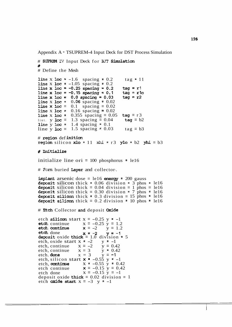
Appendix A - TSUPREM-4 Input Deck for DST Process Simulation
# SUPRD4 IV Input Deck f o r BJT Sixnulation # # Define the Mesh
l i n e x loc = -1.6 spacing = 0.2 t a g = 11 l i n e x loc = -1.05 spacing = 0.2 l i n ~ t x l o c = - 0 . 2 5 s p a c i n g = 0 . 2 t . a g = r l l inc?xloc=-0 .15spacing=O.1 t a g = r l o l i n e x l o c = 0 . 0 s p a c i n g = 0 . 0 3 t a g = r 2 line x loc = 0 -06 spacing = 0.02 l i n e x loc = 0.1 spacing = 0.02 l i n e x loc = 0.16 spacing = 0.02 l i n e x loc = 0.355 spacing = 0.05 tag = r 3 l i n t . y loc = 1.3 spacing = 0.04 tag = b2 l i n e y loc = 1.4 spacing = 0.1 line y loc = 1.5 spacing = 0.03 t ag = b3
# region def i n i t i o n region s i l i con x lo = 11 xhi = r 3 y l o = b2 yhi = b3
initialize line ori = 100 phosphorus = le16
# Fc)m buried Layer and collector -.
imp]-ant arsenic dose = le16 energy = 200 gauss deposit silicon thick = 0.06 divis ion = 3 phos = le16 depcbsit silicon thick = 0.04 divis ion = 1 phos = le16 deposit silicon thick = 0.30 divis ion = 7 phos = le16 depcs i t silican thick = 0.3 divis ion = 15 phos = le16 deposit s i l i c a n thick = 0.2 divis ion = 10 phos = le16
# Etch Collector and deposit Oxide
etch s i l i c a n start x = -0.25 y = -1 etch continue x = -0.25 y = 1.2 etch con the x = -2 y = 1.2 etch1 done x = -2 y = -1 deposit oxide thick = 1.0 divis ion = 5 etch, oxide start x = -2 y = -1 etch, continue x = -2 y = 0.42 etch, continue x = 3 y = 0.42 etch. dme x = 3 y = -1 etch, s i l i con start x = -0.55 y = -1 etch, continue x = -0.55 y = 0.42 etch continue x = -0.15 y = 0.42 etch done x = -0.15 y = -1 deposit oxide thick = 0.02 divis ion = 1 etch oxide start x = -3 y = -1

etch continue x = -3 y = 0.4 etch continue x = 2 y = 0.4 etch done x = 2 y = - 1
41 Deposit Base Contacts
cieposit silicon thick = 0.32 division = 8 phos = le16 cieposit silicon thick = 0.02 division = 1 phos = le16
4t Perform Extrinsic Base Contact Implantaticm
cieposit silicon thick = 0.03 divisicm = 3 phos = le16 implant boron dose = 4e16 energy = 40 pearson etch silicon dry thick = 0.03
4t Remve implant stop
etch silicon start x = 0 y = -1 etch continue x = O y = O . 4 etch continue x = 1 y = 0.4 etch done x = l y = - 1
4t Set-up for Contact Oxidation
cieposit oxide thickness = 0.10 division = 10
etch oxide start x = -3 y = 0.08 etch continue x = -3 y = -1 etch cantinue x = 1 y = -1 etch done x = 1 y = 0.08
i t Oxidize Base Contacts
n~ethod compress initatbe = le-10 ambient wet l.lin.0 = 3.2e4 1in.brea = 910 <loo> cliffuse wet temp = 900 time = 110 etch oxide start x = 0.12 y = -3 t?tchcontinue x = 0 . 1 2 y = 0 . 3 2 etch continue x = 2 y = 0.32 etch done x = 2 y = - 3
4f Implant Intrinsic Base
implant boron dose = 1.4e13 energy = 75 pearson
4! Fonn Sidewall Spacers
deposit nitride thick = 0.06 etch nitride dry thick = 0.09 etch oxide dry thick = 0.2 etch nitride all

# Ileposit and Define Polysilicon Emitter
deposit silicon thick = 0.39 divis ion = 12 arsenic = le21 phos = le16 deposit silicon thick = ,0.01 division = 1 arsenic = le21 1910s = le16 etch silicon start x = -3 y = -3 etch ccmtinue x = -3 y = 0.05 etch ccmtinue x = 3 y = 0.05 etch done x = 3 y = - 3 etch s i l i con start x = -3 y = -3 e tch oontinue x = -3 y = 0.15 etc:h cmt inue x = -0.165 y = 0.15 etch done x = -0.165 y = -3
# fumeal mlys i l i con Emitter
method vert ini t . t ime = 0.001 d i f fuse temp = 1000 time = 1.5 nitrogen
# Cmtact e tch over base
etch oxide start x = -1,22 y = -1 etch continue x = -1.22 y = 0.3 etch continue x = -0.87 y = 0.3 etch d m e x = -0.87 y = -1
# Dewsit conform1 alumhum layer and etch
deposit alumin th ick = 0.05 division = 1 etch alumin start x = -0.52 y = -1 etch continue x = -0.52 y = 0.5 etch ccmtinue x = -0.165 y = 0.5 etch dcme x = -0.165 y = -1
# Write the f i l e out the a PISCES-11 formatted file.
structure pisces = DST.pisout
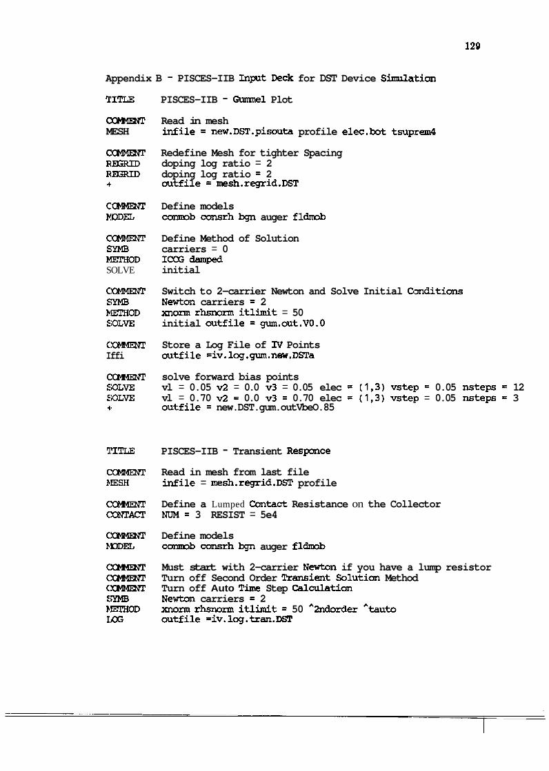
Appendix B - PISCES-IIB Inpt Deck for DST Device Simulation
TITL;E PISCES-IIB - Gu~~nel Plot
C m Read in mesh MESH infile = new.DST.pisouta profile elec.bot tsupcem4
CCMMENT Redefine Mesh for tighter Spacing RM;RID doping log ratio = 2 R B S R I D doping log ratio = 2 + outfile = mesh.regrid.DST
CCWENT Define models MODEL m b oansrh bgn auger fldmob
CCNMENT Define Method of Solution SXMB carriers = 0 ~ m m 1CYX;damped SOLVE initial
ClOMMEKT Switch to 2-carrier Newton and Solve Initial Omditians S;YMB Newtan carriers = 2 FEI'kIOD xnorm rhmorm itlimit = 50 SOLVE initial outfile = gum.out.VO.0
C!OMMENT Store a Log File of N Points Iffi outfile =iv.log.gum.nw.DSTa
CraMMENT solve forward bias points EOLVE vl = 0.05 v2 = 0.0 v3 = 0.05 elec = (1,3) vste:p = 0.05 nsteps = 12 SOLVE vl = 0.70 v2 = 0.0 v3 = 0.70 elec = (1,3) vste:p = 0.05 nsteps = 3 + outfile = new.DST.gum.outVbeO.85
TITLE PISCES-IIB - Transient Responce C m Read in mesh from last file MESH infile = mesh.regrid.DST profile
CXIMMENT Define a Lumped Cantact Resistance on the Collector <!ONTACT NUM = 3 RESIST = 5e4
CXBMENT Define models P D E L canrrob cansrh bgn auger fldmb
C- Must start with 2-carrier New- if you have a lump resistor C!CNMENT Turn off Second Order Transient Solutian Method CXMMENT Turn off Auto T h e Step Calmlatian fiYMB Newtan carriers = 2 ).EIXOD mom rhsnorm itlimit = 50 2̂ndorder ^tauto IXX3 outfile =iv.log.tran.DST
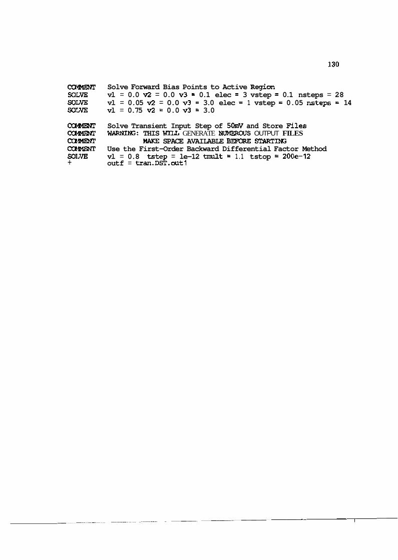
CUkBENT Solve Forward Bias Points to Active R e g i a n WLVE: vl = 0.0 v2 = 0.0 v3 = 0.1 elec = 3 vstep = 0.1 nsteps = 28 WLVE vl = 0.05 v2 = 0.0 v3 = 3.0 elec = 1 vstep = 0.05 nsteps = 14 SOjLVE vl = 0.75 v2 = 0.0 v3 = 3.0
CUWENT Solve Transient Input Step of 50mV and Store Fil!es C U m WAINIS: THIS WILG GENERATE NDEROUS OUTPUT FILES CCT- MAKE SPACE AVAILABLE BEFORE STARTINS CU4MENT Use the First-Order Backward Differential Factor Method SO],- vl = 0.8 tstep = le-12 imult = 1.1 tstop = 2006:-12 + outf = tran.DST.out1
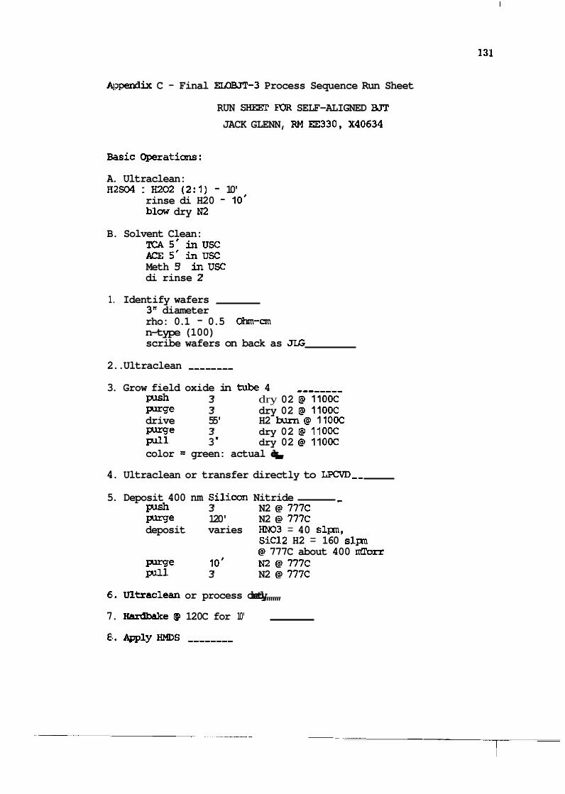
A]?pendix C - Final ELaBfi-3 Process Sequence Run Sheet
RUN SHEEZT FOR SELF-ALIGNED BJT
JACK GLENN, RM EE330, X40634
A. Ultraclean: H:2S04 : H202 (2:l) - 10'
rinse di H20 - 10' blow dry N2
B. Solvent Clean: m 5 ' i n u S C AcE5'inuSC Meth 5' inusc di rinse 2'
1. Identify wafers 3" diameter rho: 0.1 - 0.5 Ohm-cm n-type (100) scribe wafers on back as JLG
2.. Ultraclean ,,,,,--,
3. Grow field oxide in tube 4 ---,----
plsh 3' dry 02 @ 110oc Purge 3' dry 02 @ 110oc drive 55' H2 burn @ 1100C plrge 3' dry 02 @ 1100C pill 3 ' dry 02 @ 110oc color = green: actual color:,,,,,,,,,,,,
4. Ultraclean or transfer directly to LFCVD--
5. Deposit 400 nm Silicon Nitride - plsh 3' N2 @ 777C Purge 120' N2 @ 777C deposit varies HN03 = 40 slpn,
Sic12 H2 = 160 slpn @ 777C about 400 mTorr
l"=Ye 10' N2 @ 777C m l 3' N2 @ 777C
6,. Ultraclean or process directly,,,,,,,,
7. Hardbake @ 120C for 10'
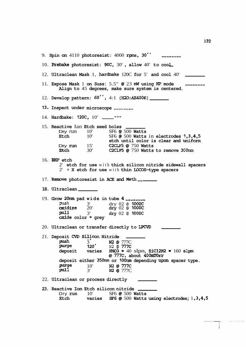
9. Spin on 4110 photoresist: 4000 rpns, 30" -------- 10. Prebake photoresist: 90C, 30' , allow 40' to cool ,,,,,,,,-
12. Ultraclean Mask 1, hardbake 120C for 5' and cool 40'
11. Expose Mask 1 on Suss : 5.5" @ 23 rnW using HP mode -------- Align to 45 degrees, make sure system is centered.
12. Develop pattern: 60", 4:1 (~20:AZ400K)
Inspect under microscope ,,,,-,,,
14. Hardbake: 120C, 10' --- 15. Reactive Ian Etch seed holes
Dry run 10' SF6 @ 500 Watts Etch 10' SF6 @ 500 Watts in electrodes 11,3,4,5
etch until color is clear and uiniform Dry run 15' C2W5 @ 750 Watts Etch 30' C2ClF5 @ 750 Watts to remove 3 0 h
16. BHF etch 2' etch for use w i t h thick silicon nitride sidewall spacers 2' + X etch for use w i t h thin LOCOS-type spacers
17. Remnre photoresist in ACE and Meth--
18. Ultraclean
19. Grow 2Onm pad wide in tube 4,,,,,,,, Plsh 3' dry 02 @ 10ooc coridize 20' dry 02 @ 1000C pull 3' dry 02 @ 100oc &de color = grey
20. Ultraclean or transfer directly to ISCVD
21. Deposit CVD Silfmn Nitride plsh 3 m @ 777C m e 120' N2 @ 777C deposit varies HN03 = 40 slpn, SiC12H2 = 160 slpn
@ 777C, about 4 0 ~ 0 r r deposit either 3 5 h or l O O n m depending upan spacer type. P 9 e 10' N2 @ 777C poll1 3' m @ 777C
22. Ultraclean or process directly
23. Reactive Ion Etch silicon nitride Dry run 10' SF6 @ 500 Watts Etch varies SF6 @ 500 Watts using electrodes; 1 ,3,4,5

remove nitride down to substrate
:24. BHF etch 20" to remove pa8 oxide -------- 125. Profile wafers to measure thickness of nitride cap -----_-_ :26. Ultraclean
:27. Reactive I m Etch substrate D r y = 10' C2ClF5 @ 750 Watts Etch 20' C2ClF5 @ 750 Watts to remove 650nm
:28. Profile wafers to measure silican step -------- :29. Examine m e wafer under S m to measure undercutting of nitride
:3 1 . Grow collector pedestal oxide in tube 4 push 3' dry 02 @ lOOOC purge 3' dry 02 @ 1000C oxidize 60 ' H2 burn @ 1000C purge 3 ' dry 02 @ 1000C pvll 3' dry 02 @ 1000C color = green
:32. Ultraclean or process directly
:33. Etch silicon nitride in H3P04 Use hottest hot plate available and reflux boiler apparatus to limit loss of water. Replace lost water peri,odically. Use the color change of field aide as a guide ko nitride ratoval. Oxide etch rate is about 1:100 to nitride etch rate.
:34. Ultraclean
:35. BHF 30" to open seed holes
:36. Rinse 10' and blow dry carefully
:37. Epitaxial lateral overgrowth of 2 - 6 m prebake 5' H2 @ 970C HC1 etch 30" HC1 = 1.5 slpn growth 20 -40' HC1 = 0.33 slpn SiC12H2 = 0.22 slpa
:38. E m u h e after growth and catalog good areas of growth ,,,,,,,,
:39. Ultraclean or process directly
40. Deposit 1.2$m m$ of CVD plysilicon -- plsh 3' N2 @ 550C W 9 e 120' N2 @ 550C
deposit 120' SiH4 = 75 slpn @ 550C, P = 1 0 M deposit 300' SiH4 = 75 sl~an@ 580C, P = 100mT m e 10' N2@550C w l 3' N2 @ 550C
41. Ultraclean or process directly -------- 42. grow 20nm aid? --------
pzsh 3 dry 02 @ 10ooc acidize 20' dry 02 @ 10OOC pill 3' dry 02 @ 10ooc
43. Planarize EL0 silica -- plrge 10' di H20 planarize 1 - 5' (1:15) Nalco 2350:di H20 observe under Namrski microscope planarize until ELX) peaks are eliminated
44. Ultraclean
45. BHF etch 30" to r e m e oxide layer
46. Hardbake @ 120C for 10' to dry
47. Apply HMDS adhesion prmter - 48. Spin on A24110 photoresist at 4000 r p s for 30" .---
49. Prebake at 90C for 30', let cool for 40' -------- 50. Ultraclean Mask 2, hardbake 120C for 5' and cool 40' - 51. Expose Mask 2 on Suss: 5.5" @ 23 rrlW using HP m d e -------- 52. Develop in 4: l ( d i H20:AZ400K) for 45 - 60"
53. Bramine under microscope
54. Hardhake at 120C for 15 minute -------- 55. Reactive Ion Etch polysilicun
Dry= 10 SF6 @ 500 Watts Etch 5 - 6' SF6 @ 500 Watts (1- for oxide color)
56. remrve photoresist in ACE and Meth
57. Ultraclean
58. Planarize base ~ t a c t s plrge 10 di HZ0 to clean wheel planarize 1' (1:15) Nalco 2350:di H20 examine under Nomarski microscope and Alphastep profilmter
planarize until the majority of wafer is flat
59. Ultraclean
60. Ian implant extrinsic base: B11, 40keV, 4.OE16cm-2 Use P < 2.OE-6 Torr and check species before impl.ant
61. BHF etch in USC to remwe all d d e aver the entire wafer
62. Hardbake at 120C for 10' to dry
64. Apply HMDS adhesian pranoter
65. Spin an AZ4110 photoresist at 4000 rpns for 30"
66. Prebake at 90C for 30 ' , let cool 40 ' -- 67. Ultraclean Mask 3, hardbake 120C for 5' and cool 40'
68. Expose Mask 3 using Suss: 5.5" @ 23 mW using HP mode
69. Develop in 4:1 AZ400K: di H20 for 60"
70. Examine under microscope
71. Hardbake at 120C for 15 mimrtes
72. Ian implant intrinsic base: B11, 90keV, 1.OE13cm-2 Use P < 2.OE-6 Torr and very low current for uniformity Perfonn dunnny implant first to obseme beam uniformity
73. Rentme photoresist using ACE and Meth ,,,,,,,_
74. Ultraclean
75. Hardbake at 120C for 10' to dry - 76. Apply HMDS adhesian pr-ter -------- 77. Spin on AZ 4110 photoresist at 4000 rpns for 30"
78. Prebake at 90C for 30', let cool for 40' -------- 79. Ultraclean Mask 2, hardbake 120C for 5' and cool 40'
80. Expose Mask 2 an Suss: 5.5" @ 23 xrW in HP mode - misalign the mask so as to expose over one corner (2 edges) of the outer edge of the base cuntacts. Fkpse the opposite corner so that all 4 edges are exposed after deve.loping the photoresist. Give about 2um of exposure for all d 4 edges of the extrinsic base ccmtacts. This is noncritical aligmnent.

81,, Develop in 4 : l AZ400K:di H20 for 60"
82 ,. Examine under microscope ,,,,,,,, Be sure all edges of the base contact are exposed and will be etched away. The idea is to remrve the outer base cca~tact seed holes and leave the inner contacts.
83. Hardbake for 10' @ 120C
84. Reactive ion etch base cantacts dry run 10' SF6 @ 500 Watts Etch 2 - 4' SF6 @ 500 Watts renrove silicon down below the seed level
85. Renrove photoresist in ACJ3 and Meth
86 :Examine under SPlI if needed to &inn removal of outer seed ,,,,,,,,
87. Ultraclean
88. Grow 2 5 h intrinsic base oxide in tube 3 (born drive :I - push 3' dry 02 @ 900C W g e 5 ' dry 02 @ 900C oxidize 142' wet 02 @ 900C bubbler @ 95C W g e 5' dry 02 @ 900C pull 3 ' dry 02 @ 900C color = gold - red
89. Ultraclean or process directly
90. Deposit 400nm of CVD polysilicon ,,,,,,,, push 3' N2 @ 550C Purge 120' N2 @ 550C deposit 330' SiH4 = 75Worr @ 550C P = 100rrll: W g e 10' N2 @ 550C Pull 3 ' N2 @ 550C
91. Ultraclean or process directly ,--
92. :Reactive ion e t ~ h sidewall spacers dry run 10 CX1F5 @ 750 w etch 12' C2ClF5 @ 750 W, look for field aude
93. IBHF to remwe oxide in emitter trench (DO W WER ETCH11 ,,,,,,,,
94. Examine under microscope: note cadition of base contact oxide--
95, Itemme photoresist in ACE and Meth,,,,,,,,
$7. Hardbake @ 120C for 10' to dry
98. Apply HMDS adhesion wcmter
99. Spin on A24110 photoresist at 4000 rpas for 30"
l80O. Prebake at 90C for 30', let cool 40'
1!01. Ultraclean Mask 5, hardbake 120C for 5' and cool 40'
1102. Expose msk 5 using Suss: 5.5" at 23 nw using HP m d e -------- 1103. Develop in 1:4 AZ4OOK:di H20 for 60"
1104. Examine under microscope to see if collectors are o,pen
1105. Hardbdke at 120C for 10' -------- '1106. BHF for 3' to open collector ccmtacts
'1107. Remnre photoresist in ACE and Meth
11 08. Ultraclean ,,,,,-,,
1109. BHF dip for 5" in ultrasanic cleaner to open emitter
1110. ~eposit 4 0 h of CVD plysilicon -------- P U S ~ 3 ' N2 @ 550C purge 120' N2 @ 550C deposit 330' SiH4 = 75 slpn @ 550C P = 100nlT plrge 10' N2 @ 550C pull 3 ' N2 @ 550C
1111. Ultraclean or process directly
'1112. Ion implant As75, 12OkeV, 5.OE15 an2
71 13. ultraclean ,---,,,,
'114. Oxidize Polysilican in tube 2 (phosphorus drive) -------- w h 3' dry 02 @ 1000C oxidize 10' dry 02 @ 10OOC oxidize 5' wet 02 @ 1000C oxidize 5' dry 02 @ 1000C pull 3 ' dry 02 @ 10ooc color = purple
1115. BHF etch for 1' to rerove oxide wer polysilicon
1116. Ultraclean or process directly --- 1117. Hardbake at 12OC for 10' to dry
1118. Apply HMDS adhesion pramter,,,,,-,,
119. Spin an A24110 photoresist at 4000 rpns for 30" -,--,---,
120. Prebake at 90C for 30', let cool for 40' ,-------
121. Ultraclean Mask 6: Polysilican definition ,,,,,-,-
122. Ekpse Mask 6 on Suss: 5.5" at 23W using HP m>de , -- 123. Develop in 1:4 AZ4OOK:di HX) for 60" ,,,,-,-,
124. Examine on microscope - 12!5. Hardbake at 120C for 15' -------- 126. Reactive ion et+ plysilicon in Drytek ,,,,,,,,
dry= 10 SF6 @ 500W etch depends SF6 @ 500W time how lcmg it takes for rings of polysiliccm to fade off of the wafer surface. Keep etching an appropriate length of time to allow for remval of the ply sidewall spacers which are on the perimeter of the device.
12;'. Renmre photoresist in ACE and Meth ,,,,,,,,
128. Ultraclean ,,,,,,,,
1251. Hardbake at 120C for 10' to dry - 1301. Apply HMDS adhesion prcanoter -- 131. Spin can A24110 photoresist at 4000 rpns for 30" ,,,,,,,,
132. Prebake at 90C for 30', let cool fur 40' ----,,,,
133. Ultraclean Mask 7: Base contact holes
134. W s e Mask 7 on Suss: 5.5" at 23nW using HP mde ,.,,,,,,,
135. Develop in 1:4 AZ4OOK:di H20 for 60" ,,,,,-,,
136. mmnine under microscope -------- 137. BHF etch for 2' to open base cuntact holes ,,,,,,,,
Use a brief -st in the USC to make sure etching starts.
139. Ultraclean ,,,,,,,,
140,, Hardbake at 120C for 10' to ,,-,,,,,

141. Apply HMDS adhesion proraoter,,,,,,--
142. Spin an AZ4110 photoresist at 4000 rpms for 30"
143. Prebake at 85$deg$C for 15' *** D m P m S * * * __-_____ 144. Ultraclean Mask 8: Metal definitiun -- 145. Eqmse mask 8 an Suss: 5.5 - 7" at 2- in HP m d e
146 ***** DO NOT HARD BAKE ***** 147. Load into Perkin-Elmer sputtering system , ,
Pump down to P < 3.OE-7 Torr Sputter/Deposit AlSiCu hreclean at 300W for 10' Sputter/Deposit AlSiCu at 100W for 30'
148. Lift-off AlSiCu: Leave in USC for a few minutes and remwe. Replace! ACE frequently. Repeat until the pattern is completely clear and no photoresist repaains. May try sodking in ACE: for 60' thenashorttimeinUSC.
149. Anneal in tube 8 for 20' at 415C in N2