Embed Size (px)
Citation preview
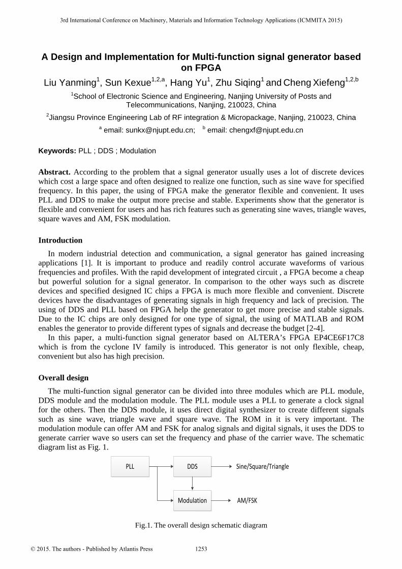
A Design and Implementation for Multi-function signal generator based on FPGA
Liu Yanming1, Sun Kexue1,2,a, Hang Yu1, Zhu Siqing1 and Cheng Xiefeng1,2,b 1School of Electronic Science and Engineering, Nanjing University of Posts and
Telecommunications, Nanjing, 210023, China 2Jiangsu Province Engineering Lab of RF integration & Micropackage, Nanjing, 210023, China
a email: [email protected]; b email: [email protected]
Keywords: PLL ; DDS ; Modulation
Abstract. According to the problem that a signal generator usually uses a lot of discrete devices which cost a large space and often designed to realize one function, such as sine wave for specified frequency. In this paper, the using of FPGA make the generator flexible and convenient. It uses PLL and DDS to make the output more precise and stable. Experiments show that the generator is flexible and convenient for users and has rich features such as generating sine waves, triangle waves, square waves and AM, FSK modulation.
Introduction In modern industrial detection and communication, a signal generator has gained increasing
applications [1]. It is important to produce and readily control accurate waveforms of various frequencies and profiles. With the rapid development of integrated circuit , a FPGA become a cheap but powerful solution for a signal generator. In comparison to the other ways such as discrete devices and specified designed IC chips a FPGA is much more flexible and convenient. Discrete devices have the disadvantages of generating signals in high frequency and lack of precision. The using of DDS and PLL based on FPGA help the generator to get more precise and stable signals. Due to the IC chips are only designed for one type of signal, the using of MATLAB and ROM enables the generator to provide different types of signals and decrease the budget [2-4].
In this paper, a multi-function signal generator based on ALTERA’s FPGA EP4CE6F17C8 which is from the cyclone IV family is introduced. This generator is not only flexible, cheap, convenient but also has high precision.
Overall design The multi-function signal generator can be divided into three modules which are PLL module,
DDS module and the modulation module. The PLL module uses a PLL to generate a clock signal for the others. Then the DDS module, it uses direct digital synthesizer to create different signals such as sine wave, triangle wave and square wave. The ROM in it is very important. The modulation module can offer AM and FSK for analog signals and digital signals, it uses the DDS to generate carrier wave so users can set the frequency and phase of the carrier wave. The schematic diagram list as Fig. 1.
PLL DDS
Modulation AM/FSK
Sine/Square/Triangle
Fig.1. The overall design schematic diagram
3rd International Conference on Machinery, Materials and Information Technology Applications (ICMMITA 2015)
© 2015. The authors - Published by Atlantis Press 1253

Design of the PLL module A phase-locked loop or a PLL is a system which can generate an output signal whose phase is
decided by the input signal. Although there are many different types of PLLs, it is easy to explain it as an electronic circuit which consists of a frequency oscillator and a phase detector. The PLL starts with a stable crystal reference frequency which is one of the inputs to the phase detector. The phase detector outputs a signal that has an average value that is proportional to the phase error between the comparison frequency and the output frequency. Then the signal makes oscillator to keep the phases matched. The whole progress is just like a loop.
PD LF VCO
/M
fin fout
Fig. 2. The PLL module schematic diagram
In this module, as shown in Fig.2, it consists four parts which are a phase detector, a low pass filter, a variable frequency oscillator and a /M divider. We can use a crystal oscillator to create fin and use the /M divider to get the frequency we want. Using a PLL can help us to get a pure and precise frequency which we use it to be the clock frequency or fclk. The implementation is based on ALTERA’s FPGA EP4CE6F17C8; we can use the IP core in QUATUS II to build it. Over all is the design of the PLL module.
Design of the DDS module
A DDS or direct digital synthesizer, produces an analog waveform—usually a sine wave, but triangular and square waves are inherent—by generating a time-varying signal in digital form and then performing a digital-to-analog (D/A) conversion. DDS devices are primarily digital, so they can offer fast switching between output frequencies, fine frequency resolution, and operation over a broad spectrum of frequencies. DDS is based on the sampling theorem, and can control the frequency of the output waveform. The DDS module is the most important module in this design.
As shown in Fig. 3,in this multi-function signal generator, the module contains five parts. The first part is the frequency control register, its initial value is zero. Then when it comes to the rising edge of fclk, the frequency control register send its value to adder with variable M which is set by person. When the frequency control register is over flown, the phase control register plus one and the remainder becomes the value of the frequency control register. So we can set the frequency of the signal by changing the value of M. The equation is as below in which N is the size of the frequency control register.
Nout Mff 2/*clk= (1)
Frequency Control Register
Phase Control Register∑ ROM DAC LPF
fout
fclk
choose
Fig. 3. The DDS module schematic diagram
The second part is the phase control register which send its value to the ROM when it comes to the rising edge of fclk.We can set the phase of the signal by changing the initial value of the phase control register. Then the third part is the ROM. It contains three small ROMs in which stored the sine table, the square wave table and the triangle wave table. All the three tables can be created by
1254

Matlab or C++. User can choose to use which ROM depending on which signal he wants to generate. When it comes to the rising edge of fclk, the ROM use the address which is received by the phase control register to search for the value and send the value to the next part, the DAC.A DAC or digital-to-analog converter is a chip that can change digital signals to analog signals. The FPGA pins produce the digital signals but the generator finally generates the analog signal. The fifth part is the LPF or low pass filter which can filter the noise and useless high frequency components. Over all is the design of the DDS module.
Design of the Modulation module This multi-function signal generator can also generate modulation signal by AM and FSK. Frequency-shift keying (FSK) is a frequency modulation scheme in which digital information is
transmitted through discrete frequency changes of a carrier wave [5]. As shown in Fig. 4,it is easy to realize. When the data comes to the selector, if the data is 1 then
the variable M in DDS module will be assigned M1 or M2 while the data is 0.As it is said in the DDS module, the change of M brings the change of the frequency so we can get two signals in different frequencies.
DDSM1
DDSM2
Yes No
=1
fin
fout1 fout2
Fig. 4. The FSK module schematic diagram Amplitude modulation or AM is one type of the modulation techniques used in communication.
It uses the amplitude of the carrier wave to transmit information which means the amplitude of the carrier wave changes with the changing of the modulating signal but the carrier’s frequency is unchanged.
Multiplier Adder Multiplier
x(nTs)
M
1 Carrier wave
s(nTs)
Fig. 5. The AM module schematic diagram In a signal generator, AM is a basic function. We can see the schematic diagram in Figure 5.
According to FPGA is a digital chip, it can only deal with digital signals. The equation in discrete mathematics is as below:
scss nTnTMxnT ωcos)](1[)(s += (2)
M is AM depth and cω is the angular frequency of carrier wave. Ts is the sampling interval. The two multipliers can also use ALTERA’s IP core. However there is one more thing need to do
1255

which is the transform from unsigned to signed. Usually we get the signal we want to send form AD and the data is unsigned but the AM modulation need two signed data to multiply so we need to do some transformation. Also, when we finally get the modulated signal s(nTs),we also need to transform it to a unsigned data because the DA must deal with the unsigned data.
Test results The sine signal the generator created can be seen in Figure 6 and the AM signal the generator
created can be seen in Fig.7.
Fig. 6. The sine signal Fig. 7. The AM signal
Conclusion Nowadays the signal generators are widely used in a lot of fields. Many large companies devote
a lot to this field. This paper focus on a flexible signal generator with high cost performance. The use of PLL and DDS technologies enable it to have functions not only generate single sine wave but also can modulate other signals. Besides a FPGA also helps it to achieve the goal of flexible and convenient multi-function signal generator design.
Acknowledgement This research was financially supported by the National Natural Science Foundation of China
(Grant No.61271334), Natural Science Foundation of the Jiangsu Higher Education Institutions of China (Grant No. 15KJD510001), and Natural Science Foundation of Nanjing University of Posts and Telecommunications(Grant No. NY214049).
References
[1] Zhiqiang Zhang; Feng Dong. A harmonic signal generator based on DDS and SOPC. Control and Decision Conference (CCDC) , 2010. 1542 - 1547
[2] Banerjee, Dean (2006), PLL Performance, Simulation and Design Handbook (4th ed.), National Semiconductor
[3] Xiaochu Wang, Qiujun Mei. High-Precision Design of DDS Based on FPGA. Intelligent Systems (GCIS), 2012 Third Global Congress , 2012. 386-389
[4] Kennedy, G.; Davis, B. (1992). Electronic Communication Systems (4th ed.). McGraw-Hill International. ISBN 0-07-112672-4, p 509
[5] Lisha YAN, Wei.WEI Implementation of Digital Amplitude Modulation Based on FPGA[J]. Instrument Technique and Sensor, 2011, (05)
1256