Embed Size (px)
Citation preview

FULLPAPER
www.afm-journal.dewww.MaterialsViews.com
1930
A Controllable Self-Assembly Method for Large-ScaleSynthesis of Graphene Sponges and Free-StandingGraphene Films
By Fei Liu and Tae Seok Seo*
A simple method to prepare large-scale graphene sponges and free-standing
graphene films using a speed vacuum concentrator is presented. During the
centrifugal evaporation process, the graphene oxide (GO) sheets in the
aqueous suspension are assembled to generate network-linked GO sponges
or a series of multilayer GO films, depending on the temperature of a
centrifugal vacuum chamber. While sponge-like bulk GO materials (GO
sponges) are produced at 40 -C, uniform free-standing GO films of size up to
9 cm2 are generated at 80 -C. The thickness of GO films can be controlled
from 200 nm to 1mm based on the concentration of the GO colloidal
suspension and evaporation temperature. The synthesized GO films exhibit
excellent transparency, typical fluorescent emission signal, and high flexibility
with a smooth surface and condensed density. Reduced GO sponges and
films with less than 5wt% oxygen are produced through a thermal annealing
process at 800 -Cwith H2/Ar flow. The structural flexibility of the reduced GO
sponges, which have a highly porous, interconnected, 3D network, as well as
excellent electrochemical properties of the reduced GO film with respect to
electrode kinetics for the [Fe(CN)6]3�/4� redox system, are demonstrated.
1. Introduction
The superlative properties of graphene have recently beendemonstrated theoretically and experimentally.[1] In particular,the high mobility and saturation velocity for both electrons andholes, excellent chemical stability and mechanical strength, andgood optical transparency make graphene a promising nanoma-terial for advanced electronic applications.[2,3] Research wasinitially focused towards obtaining ahigh-quality two-dimensionalgraphenemonolayer to take full advantages of these extraordinaryproperties.[4–6] On the other hand, attempts to generate large-areagraphene sheets have been made with a view to application inflexible displays, alternative electrodes, and as transparentconducting film for solar cells.[7–9] To date, several methods havebeen developed for preparation of a large-area graphene film,including micromechanical exfoliation of graphite,[10] chemical
[*] Prof. T. S. Seo, Mr. F. LiuDepartment of Chemical and Biomolecular Engineering (BK21program) and Institute for the BioCenturyKAIST 335 Gwahangno, Yuseong-gu, Daejeon 305-701 (Korea)E-mail: [email protected]
DOI: 10.1002/adfm.201000287
� 2010 WILEY-VCH Verlag GmbH & Co. KGaA, Weinheim
vapor deposition (CVD) and epitaxialgrowth on a nickel or silicon carbidesurfaces,[11–13] and liquid-phase exfoliationof graphite in organic solvents.[14]However,mechanical exfoliation of highly orderedpyrolytic graphite or liquid-phase basedexfoliation result in a relatively small size(nm tommscale in the lateral dimension) ofgraphene, while thermal decomposition ofSiC, or epitaxial growth onmetal substratesby CVD methods is constrained by its highcost and lack of controllability for forminghomogenous large-area films.
As an alternative method, a graphiteoxide-based film fabrication method wasproposed as being fast, simple and cost-effective. As originally reported byHummers et al., graphite oxide has beenconsidered as a promising precursor to theformation of graphene materials via areduction process.[15] Abundant functionalgroups, such as epoxy, hydroxyl, andcarboxylic acid, at the edges and in the
plane contribute to the high stability of homogeneous graphemeoxide (GO)suspensions inaqueous andorganic solvents, so that anassembly of these well-dispersed oxidized graphene sheetsgenerates ordered macrostructures.[16] Recently, Ruoff et al.reported the fabrication of free-standingGOfilms by flow-directedassembly of individual GO sheets through filtration; the resultingGOfilms showed excellent physical properties in termsof stiffnessand mechanical strength.
Langmuir-Blodgett assembly of GO sheets in a layer-by-layermanner, spin-coating techniques on a SiO2/Si substrate, thermalevaporation to assemble GO sheets at a liquid-air interface, andelectrophoretic deposition on an ITO substrate have also beenproposed as methods to generate large transparent GO films; thesynthesized GOfilms could be further transformed into graphenefilms by reduction with hydrazine or a thermal annealingmethod.[17,18]
Although several of themethods tomake graphene-oxide-basedmembranes described above are facile and relatively simple, allrequire the assistance of either various substrates, such asAnodiscTMmembrane, silicon and glass, or conductive electrodesandpower supplies. In the case ofwetGOfilmsgenerated, a dryingprocess is required, which is time-consuming. Spurred by thephenomenon that the combination of gravity, centrifugal force,vacuum evaporation and hydrodynamics of homogeneous GO
Adv. Funct. Mater. 2010, 20, 1930–1936

FULLPAPER
www.MaterialsViews.comwww.afm-journal.de
suspensions could lead to well-ordered films by self-assembly ofGO sheets, herein we present much simpler synthetic techniquesto obtain both large-scale free-standing GO thin films and sponge-like GO bulk materials – called GO sponges – using a speedvacuum concentrator and without the need for substrates,electrodes or further drying steps. In the process of evaporatingcolloidal GO suspensions by the vacuum centrifugal evaporator,macroscopic multilayered GO membranes were fabricated in alayer-by-layermanner through the self-assembly ofGOsheets, andtheir thickness could be easily tuned by controlling theconcentration of GO. Interestingly, the temperature of a speedvacuumconcentrator affects the evaporation rate ofGOsheets andthe assembly dynamics, resulting in unique GO sponges at lowtemperature that have a three-dimensional interconnected net-work of GO sheets. Morphological and compositional character-izations of the resultant GO sponges and films, as well as theirreduced forms, were performed by scanning electron microscopy(SEM) and X-ray photoelectron spectroscopy (XPS); their opticaland electrical properties were also evaluated by UV/vis/NIRspectrophotometry and cyclic voltammetry.
2. Results and Discussion
2.1. Synthetic Mechanism of Graphene Oxide Sponges and
Films
A schematic illustration for generating GO sponges and GO filmsin a speed vacuum concentrator is presented in Figure 1. Thehomogeneous suspensions of single-layered GO sheets were
Figure 1. Synthetic process for the fabrication of GO sponges and films by s
mictrotube. b) Schematic illustration of the produced GO sponges and films at
image for GO sponges prepared at 40 8C (upper panel), and multilayer GO film
GO films recovered from an Eppendorf tube; a representative image of 3 cm d
H2/Ar at 800 8C for 12 h; the elastic property of the reduced GO sponges was
structure. f) Free-standing graphene films prepared after thermal annealing
Adv. Funct. Mater. 2010, 20, 1930–1936 � 2010 WILEY-VCH Verl
produced by sonication of graphite oxide in an aqueous solutionaccording to the well-known modified Hummers method.[19,20]
1mL of GO colloidal suspension prepared in a 2mL microtube(Figure 1a), was placed on the rotor plate fixed in the vacuumchamber. The vacuumcentrifugal evaporator operates at a rotatingspeed of 1 800 rpm under 1� 10�4 torr pressure, and thecombination of vacuum, applied to the sample chamber froman external source, and centrifugal action promotes solventevaporation without sample loss due to foaming or bumping. TheGO sheets in a colloidal suspension can be simply assembled bythe combined effect of the vacuum evaporation, temperature of avacuum chamber and centrifugal force.
When the temperatureof the vacuumchamberwas controlled at40 8C, only GO sponges were generated and stacked on the innerwall of the microtube after 4 h evaporation process (Figure 1b). Atthis low temperature, the GO sheets are likely to form theirnetwork via van der Waals force during water evaporation due tothe outward centrifugal force that is more dominant than theupward evaporation force. The resultant GO sponges, collectedfrom themicrotube by a tweezer, showed a browncolor and cotton-like soft morphology (Figure 1c).
When the temperature of the vacuumchamberwas increased to60 8C, one layer of GO films was generated at the liquid/airinterface, along with GO sponges as the main product stackedbeneath the GO film.
When the temperature of the vacuum chamber was fixed at80 8C, about 11 layers of shiny brown and transparent GO filmswere produced from top to bottom in themicrotube (Figure 1b). Atthis high temperature, the evaportion rate was accelerated andGOsheets tend to assemble with each other at the liquid/vacuuminterface rapidly to form the first GO film layer. Subsequently, thesecond layerGOfilmwas generatedunder thefirstGOfilmby self-
peed vacuum centrifugation. a) 1mL GO solution (3mgmL�1) in a 2mL
different temperatures of the vacuum centrifugation chamber, and a digital
s prepared at 80 8C (lower panel). c) The GO sponges, and, d) free-standing
iameter GO film (inset). e) Reduced GO sponges after thermal annealing in
demonstrated by observing the recovery to the flat shape from the folded
in H2/Ar at 800 8C for 12 h. The scale bar represents 1 cm in c–f.
ag GmbH & Co. KGaA, Weinheim 1931

FULLPAPER
www.afm-journal.dewww.MaterialsViews.com
1932
assembly of GO sheets; this process proceeded continuously,leading to a series of GO films from top to bottom inside themicrotube. With care, we could peel off the generated GO filmsone-by-one, and oval-shaped GO films were successfully obtainedas free-standing product with an average length of 1.5 cm(Figure 1d). By adjusting the concentration of theGO suspensionsfrom 2 to 5mgmL�1, we could tune the thickness of GO filmsbetween 250 nm and 1mm.
Note that no complicated deposition instruments, such assubstrates or post-treatment processing, were necessary in ourvacuum centrifugal evaporating method. Larger area GO filmscould be obtained simply by employing a larger tube to expand thearea of the liquid/air interface. Using a 50mL tube, a 3 cmdiameter GO film was generated at 80 8C (Figure 1d, inset).
We subsequently performed the reduction process for theproducedGO sponges and films by thermal annealing at 800 8C inH2/Ar 1:4 with a flow rate of 50 cc min�1 for 12 h to recover an sp2
graphene structure. The sponge and film morphology waspreserved after reduction, and the reduced forms exhibited theirown graphitic color, a metallic luster as shown in Figure 1e and f.The elastic property of the reduced GO sponge was demonstratedby showing that the GO sponge bent to a large degree by a pincettewas recovered to the original flat configuration by itself (Figure 1e,inset) due to the strongnetworkconnectionof theGOsheetswhichwas proven by SEM as below.
Figure 2. a) Low-, and, b) high-magnification SEM images of an inner part
of GO sponges. c) The outer part of GO sponges, as formed close to the
wall of a tube. d) SEM image for the morphology of graphene sponges after
thermal annealing treatment in H2/Ar at 800 8C for 12 h. e) HR-TEM data
for the single layered graphene sheet isolated from the reduced GO
sponges by sonication, and, f) an electron diffraction pattern which was
taken at the periphery of the graphene sheet in e. The scale bars represent
100mm in a and c, 10mm in b, 50mm in d, and 500 nm in e.
2.2. SEM of GO Sponges
Figure 2a–d shows SEM images ofGO sponges. Figure 2a displaysa porous morphology of GO sponges at low magnificationresolution, and a close-up view inside GO sponges reveals thatindividual GO sheets ranging from 200 nm to 5mm arecrosslinked to form a ca. 30mm GO assembler network viamainly edge-to-edge and partially edge-to-surface interactions(Figure 2b). On the other hand, the part of theGO sponges formedcloser to the inner wall exhibited parallel linkages of GO sheetswith a relatively uniform thickness and size distribution, probablydue to the ordered stacking of GO sheets by the centrifugal force(Figure 2c).When the as-synthesizedGOspongeswere reducedbythermal annealing, the brown color of GO sponges turned to blackand the porosity of the GO sponges was diminished as thefunctional groups on theGOfilmwere evaporated bywater,CO2 orCO molecules. However, the randomly connected morphology ofthe GO sponges was maintained with a large surface area(Figure 2d).
We sonicated the reduced GO sponges for 1 h in propan-2-ol inthe hope that the individually connected graphene sheets could berecovered as a monolayer.[14] We hypothesized that the end-to-endinteraction energy of graphene sheets in the sponges withmicrospace should bemuch less than that of the pristine graphitesin which the graphene layers are tightly held by a p–p stacking in aface-to-face manner, so the single layered graphene fabricationfrom graphene sponges would be more efficient. It was observedthat the graphene dispersion rate from the reduced GO spongeswas faster than that of the pristine graphites due to the relativelyweaker bonding between the neighboring graphene sheets, andisolated graphene was characterized by high resolution
� 2010 WILEY-VCH Verlag GmbH & C
transmission electron microscope (HR-TEM) (Figure 2e). Sincethe GO sheets were initially connected to each other edge-to-edge,the open side of GO sheets was likely to be scrolled during thereduction process, resulting in a heavily folded structure at edges.A selected area electron diffractionpattern image shows the clearlyordered crystal structure of graphene and the relative intensity ofthe inner peaks {1100} of six-fold symmetry diffraction pattern ismore intense than the outer {2110} peaks, which confirms thegeneration of monolayer graphene from the reduced GO sponges(Figure 2f).[14]
These results demonstrate that the reduction of GO spongesrecovers the natural graphene structure and simple sonicationprocess disconnects the 3Dnetwork of graphene sheets to producea single-layered graphene. We expect that the resultant GOsponges, having microporosity, large surface area and graphenenetworks, could find a variety of applications including molecularstorage, catalytic support and compositematerials. In addition, thereduced GO sponges can be a source for monolayer graphenefabrication through simple sonication without any toxic organicsolvents,[21] ionic stabilizers[22] or surfactants.[23]
o. KGaA, Weinheim Adv. Funct. Mater. 2010, 20, 1930–1936

FULLPAPER
www.MaterialsViews.comwww.afm-journal.de
2.3. Transmittance and Photoluminescence Properties of GO
Films
The optical properties of the GO films were characterized bytransmittance and photoluminescence. The 400 nm thick GOfilms have such an excellent mechanical strength that designedshapes can be easily manipulated by using a blade or scissors andimmobilized on substrates such as a siliconwafer and a glass slide.The optical transmittance measured by a UV/vis/NIR spectro-metrywas about 52.0%at awavelength of 550 nmand increases upto 69.4% in the NIR region. A thinner 200 nm thick GO filmexhibited higher transmittance of 76% at 550 nm and 89% at2 000 nm (Figure 3a), demonstrating that the uniform and denselyorganized assembly of the GO sheets by our methods contributesto the excellent transparency of the GO films. The recombinationof electron–hole pairs localizedwithin the sp2 carbondomain in sp3
matrix leads to a unique photoluminescence of GO films at ca.546 nm.[24–26] Thus, rectangular, trapezoidal, and triangularshapes of GO films generated a green fluorescence signal whenscanned at an excitation wavelength of 532 nm (Figure 3b). This
Figure 3. a) Transmittance of 200 and 400 nm thick-GO filmsmeasured by
UV/vis/NIR spectrometry (the Kaist logo is beneath the film). b) Different
patterned GO films show a unique florescent emission signal with 532 nm
excitation.
Adv. Funct. Mater. 2010, 20, 1930–1936 � 2010 WILEY-VCH Verl
fluorescent emission property of GO films could prove useful inthe development of novel biosensors and optoelectronic devices,when combined with the capability of versatile surface modifica-tion with various organic or biomolecules by employing theabundant functional groups on the GO surface.
2.4. SEM of GO Films
The SEM image of aGOfilm in Figure 4a exhibits an ultra-smoothsurfacewithout anyporesor sharpedges, showing that the vacuumcentrifugal evaporation process at high temperature renders theefficient assembly of GO sheets that are more compact andoriented than those obtained from electrophoretic deposition andheated evaporationmethods. The atomic force microscopy (AFM)data show that the surface roughnessof the as-synthesizedGOfilmwas approximately 50 nm (Figure S1, see the SupportingInformation).[20,27]
The high mechanical strength of GO film derived from thedensely packed structure was proven by folding it with a curvatureradius of 50mm using tweezers, as shown in Figure 4b.
After reduction by thermal annealing in H2/Ar, the originalbrown color of GO films was changed to black with a shiny lusterwithout visual transparency, and became more fragile than theoriginal GO films. A reduced GO film had many bubble shapeswith adiameter of 30mmdue to thedecompositionof labile oxygenfunctional groupson the surface (Figure 4c).Across-sectional viewof the reducedGO sheets displayed orderedmultilayer stacks witha thickness of 400 nm (Figure 4d). Even after thermal evaporation,the layer-by-layer assembled structure was well-maintained,demonstrating the high integrity and stability of the reducedGO films, and the close contact between layers can minimize the
Figure 4. a) Lowmagnification SEM image of a 400 nm thick GO film, and,
b) a side-view of highly flexible GO film. c) SEM images for the surface of
the reduced GO film, and, d) a cross-sectional SEM image of the reduced
GO film. The scale bars represent 50mm in a, 40mm in b, 30mm in c, and
200 nm in d.
ag GmbH & Co. KGaA, Weinheim 1933

FULLPAPER
www.afm-journal.dewww.MaterialsViews.com
1934
barrier for electron transfer, thereby enhancing the electronic andelectrochemical properties.
2.5. X-ray Photoelectron Spectroscopy (XPS) of the Reduce GO
Films
AlthoughGOfilmsare considerednot to be electrically conductive,the reduction process by thermal annealing or chemical reducingagents recovers the sp2 carbon network of graphene, rendering thereduced GO be highly conductive. Thermal annealing under H2
gas is known to be the most effective reducing method.[18] Thecompositional analysis and quantitative weight percentage (wt%)of carbon and oxygen on the GO film were monitored at differentreduction times by XPS and energy dispersive X-ray spectroscopy(EDX).Whereas theGOfilm initially exhibited a considerably highoxygen signal, after 12 h reduction therewas a significant decreasein the O 1s peak, implying the efficient removal of oxygen-containing functional groups (Figure 5a). In particular, the GOfilms represented four kinds of oxygen-containing carbons:carbon–hydroxyl groups (C�OH) at 285.7 eV, epoxy/ether groups(C�O) at 286.7 eV, carbonyl groups (C¼O) at 288.0 eV andcarboxylate carbongroup (O�C¼O)at 289.4 eV, in addition tonon-oxygenated C at 284.8 in the C 1s XPS spectrum (Figure 5b).[28,29]
The oxygen peakwas almost completely suppressed after 12 h, andthe C 1s XPS showed only the graphitic carbon (Figure 5d).Accordingly, the EDX data of the GO film revealed that 32.34wt%of oxygen and 67.66wt% of carbon were situated on the GO film(Figure S2, see the Supporting Information). After 6 h thermalannealing, the peak intensities of oxygen-containing carbons
Figure 5. a) XPS spectra of the GO and reduced GO films after 6 and 12 h
thermal annealing, and b–d) their corresponding C 1s XPS spectra.
� 2010 WILEY-VCH Verlag GmbH & C
drastically decreased from35.43 to 9.28wt%,with a correspondingincrease in the peak of graphitic carbon atoms from 64.57 to90.72wt%. The weight percentage of carbon atom after 12 hannealing time reached more than 95wt%, a much higher valuethan those previously reported.[30,31]
The fact that the sp2-conjugated honeycomb carbon crystallattice was sufficiently regenerated and the interlayer distancebetween graphene stacks was decreased by completely removingthe oxygenous functional group can provide the reduced GO filmwith excellent conductivity. The average surface resistance of thereduced graphene film was measured as 106.85 V sq�1 at roomtemperature by using a standard four point probe, and such a lowresistance makes the reduced GO film a promising electronicmaterial.
2.6. Electrochemical Behavior of the Reduced GO Film
In order to evaluate the electrochemical properties of the reducedgraphene film, the cyclic voltammetric (CV) response wasinvestigated. The graphene film was used as a working electrodewith respect to the electron-transfer in the [Fe(CN)6]
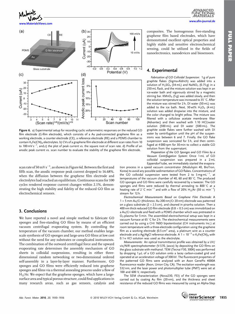
3�/4� redoxsystem. This redox system is widely employed to evaluate theelectrochemical behavior of carbon-based materials due to itshighly sensitive response to the electronic properties, surfacemicrostructure and surface chemistry of carbon electrodes.[32] Theexperimental setup (Figure 6a) consists of the graphene film,which was attached on the gold electrode and fixed with apolydimethylsiloxane (PDMS) chamber, a Pt wire as a counterelectrode, and a Ag/AgCl reference electrode. The exposed area ofthe graphene film was 0.5 cm2, and the PDMS chamber was filledwith a 1� 10�3
M K3Fe(CN)6 and 0.1 M KCl electrolyte.Cyclic voltammograms on the graphene film electrode were
recorded at different scan rates from 10 to 100mVs�1 with apotential range from�0.2 to 0.8 V (Figure 6b). A series of perfectlyreversibleCVprofileswere obtainedwith apair ofwell-defined andpeak-shaped redox wave. While the anodic peak potential (Epa)moved in a positive direction as the scan rate increased, thecathodic peakpotential (Epc)moved in anegative direction, therebyproducing a gradual increment of a peak-to-peak potentialseparation (DEp) with a formal potential that was almost constant(264mV). TheDEpwas 106mVat 100mVs�1 scan rate, and60mVat 10mVs�1, which corresponds to the ideal value of 59mV,[33]
suggesting a high electron-transfer of [Fe(CN)6]3�/4� at the
graphene film surface due to a zero-bandgap property.In proportion to the scan rate, both the absolute value of anodic
(Ipa) and cathodic peak current (Ipc) became larger, whilemaintaining the ratio of the Ipa to Ipc as 1.0, and showed a linearrelationship with the square root of the potential scan rate. Thelinear regression equations can be expressed asIpa¼ 2.8749vþ 1.6951 (Ipa: mA, v: ðVs�1Þ
1=2, correlation coeffi-cient: 0.9958) and Ipc¼� 3.092v�1.3989 (Ipc: mA, v: ðVs�1Þ1=2,correlation coefficient: 0.9983) (Figure 6c). This perfectly linerrelationship indicates that the electrochemical reaction iscontrolled by a semi-infinite linear diffusion based redox processfrom the electrolyte to the graphene film electrode surface.
The electrochemical stability of the graphene film electrodewasfurther evaluated by increasing the number of scan up to 100 at a
o. KGaA, Weinheim Adv. Funct. Mater. 2010, 20, 1930–1936
FULLPAPER
www.MaterialsViews.comwww.afm-journal.de
Figure 6. a) Experimental setup for recording cyclic voltammetric responses on the reduced GO
film electrode (G-film electrode), which consists of a Au pad-connected graphene film as a
working electrode, a counter electrode (CE), a reference electrode (RE) and a PDMS chamber to
contain K3Fe(CN)6 electrolytes. b) CVs of a graphene film electrode at different scan rates from 10
to 100mV s�1, and,c) the plot of peak current vs. the square root of scan rate. d) Profile of an
anodic peak current vs. scan number to evaluate the stability of the graphene film electrode.
scan rateof 50mVs�1, as shown inFigure6d.Between thefirst andfifth scan, the anodic response peak current dropped to 16.68%,when the diffusion between the graphene film electrode andelectrolytes had reached an equilibrium.Continuous scans for 100cycles rendered response current changes within 2.1%, demon-strating the high stability and fidelity of the reduced GO film aselectrochemical sensors.
3. Conclusions
We have reported a novel and simple method to fabricate GOsponges and free-standing GO films by means of an efficientvacuum centrifugal evaporating system. By controlling thetemperature of the vacuum chamber, our method enables large-scale synthesis of GO sponges and large-area GO films at low costwithout the need for any substrates or complicated instruments.The combination of the outward centrifugal force and the upwardevaporating rate determines the assembly mechanism of GOsheets in colloidal suspensions, resulting in either three-dimensional random networking or two-dimensional orderedself-assembly in a layer-by-layer manner. Furthermore, GOsponges and GO films were efficiently reduced into graphenesponges and films via a thermal annealing process under a flow ofH2/Ar. We expect that the graphene sponges, which have a large-surface area and typical porous structure, couldfindapplications inmany research areas, such as gas sensors, catalysis and
Adv. Funct. Mater. 2010, 20, 1930–1936 � 2010 WILEY-VCH Verlag GmbH & Co. KGaA,
composites. The homogenous free-standinggraphene film based electrodes, which havedemonstrated excellent optical properties andhighly stable and sensitive electronchemicalsensing, could be utilized in the fields ofnanoelectronics, nanodevices and biosensors.
4. Experimental
Fabrication of GO Colloidal Suspension: 1 g of puregraphite flakes (Sigma-Aldrich) was added into asolution of H2SO4 (34mL) and NaNO3 (0.75 g) in a250mL flask, and the mixture solution was kept in anice-water bath and vigorously stirred by a magneticstirring bar. KMnO4 (5 g) was added slowly, and thenthe solution temperature was increased to 35 8C. Afterthe mixture was stirred for 2 h, DI water (50mL) wasadded to the ice bath. Next, 30wt% H2O2 (4mL)solution was added dropwise into the mixture, andthe color changed to bright yellow. The mixture wasfiltered with a cellulose acetate membrane filter(Advantec) and then washed with 1:10 HCl/watersolution (500mL) and DI water (500mL). Thegraphite oxide flakes were further washed with DIwater by centrifugation until the pH of the suspen-sions was between 6 and 7. Finally, the GO flakesuspension was sonicated for 5 h, and then centri-fuged at 4 000 rpm for 30min to collect a stable GOsolution from the supernatant.
Preparation of the GO Sponges and GO Films by aVacuum Centrifugation System: Once 1mL of GOcolloidal suspension was prepared in a 2mLEppendorf tube, we immediately started the evapora-
tion process in a speed vacuum concentrator (Modulspin 40, BioTron,Korea) to avoid any possible sedimentation of GO flakes. Concentrations ofthe GO colloidal suspension were tested from 2 to 5mgmL�1, attemperatures of the vacuum chamber of 40, 60 and 80 8C. The producedGO sponges and GO films were carefully recovered by a tweezer. The GOsponges and films were reduced by thermal annealing to 800 8C at aheating rate of 2 8C min�1 and with a flow of 20% H2/Ar (50 cc min�1)stream for 12 h.
Electrochemical Measurements Based on Graphene Film Electrode: A1� 5mm Au/Cr (thickness: Au 200 nm/Cr 20 nm) electrode was patternedon a glass substrate (2� 2.5 cm), and cleaned in piranha solution. Then a400 nm thick reducedGO film electrode (0.8� 0.5 cm) was immobilized ona Au/Cr electrode and fixed with a PDMS chamber which was pretreated inO3-plasma for 5min. The assembled electrochemical setup was kept in avacuum furnace at 65 8C for 2 h. The electrochemical measurements werecarried out by using a CHI 760D bipotentiostat (CH instruments Inc.) atroom temperature with a three-electrode configuration using the graphenefilm as a working electrode (0.5 cm2 area), a platinum wire as a counterelectrode and a Ag/AgCl reference electrode. A 1� 10�3
M K3Fe(CN)6 with0.1 M KCl solution was used as the electrolyte.
Measurements: An optical transmittance profile was obtained by a UV/vis/NIR spectrophotometer (V-570, Jasco) by depositing the GO films onthe glass substrate with methanol. TEM (Tecnai F30, 300K) was performedby dropping 1mL of a GO solution onto a lacey carbon-coated grid andoperated at an acceleration voltage of 300 kV. The fluorescent properties ofthe patterned GO films were analyzed with an Axon GenePix 4000Afluorescence reader (Axon, Union City, CA). The excitation wavelength was532 nm, and the laser power and photomultiplier tube (PMT) were set at100 and 600 V, respectively.
The SEM characterization (Nova230, FEI) of the GO sponges werecarried out by coating Au film (20 nm), and the thickness and sheetresistance of the reduced GO films was measured by using an Alpha-Step
Weinheim 1935

FULLPAPER
www.afm-journal.dewww.MaterialsViews.com
1936
surface profiler (Tencor, USA), and a standard 4-point probe method (AiT,Korea) respectively. The surface roughness and morphology was measuredby AFM (SPA 400, Seiko Instruments) with a tapping mode and a256� 256 pixel resolution. XPS was performed on ESCA 2000Multilab (VGMicrotech) system using MgKa (hn ¼1 253.6 eV) with a residual gaspressure in the range of 10�10 Torr.
Acknowledgements
We acknowledge financial support from the Korean Ministry ofEnvironment under the ‘‘Eco-Technopia 21’’ Project. Supporting Informa-tion is available online from Wiley InterScience or from the author.
Received: February 11, 2010
Revised: March 12, 2010
Published online: May 20, 2010
[1] A. K. Geim, Science 2009, 324, 1530.
[2] A. K. Geim, A. H. Macdonald, Phys. Today 2007, 60, 35.
[3] A. K. Geim, K. S. Novoselov, Nat. Mater. 2007, 6, 183.
[4] K. S. Novoselov, D. Jiang, F. Schedin, T. J. Booth, V. V. Khotkevich,
S. V. Morozov, A. K. Geim, Proc. Natl. Acad. Sci. U. S. A. 2005, 102, 10451.
[5] C. Berger, Z. Song, X. Li, X. Wu, N. Brown, C. Naud, D.Mayou, T. Li, J. Hass,
A. N. Marchenkov, E. H. Conrad, P. N. First, W. A. de Heer, Science 2006,
312, 1191.
[6] M. I. Katsnelson, Mater. Today 2007, 10, 20.
[7] X. Li, G. Zhang, X. Bai, X. Sun, X. Wang, E. Wang, H. Dai,Nat. Nanotechnol.
2008, 3, 538.
[8] G. Eda, G. Fanchini, M. Chhowalla, Nat. Nanotechnol. 2008, 3, 270.
[9] Z. Liu, Q. Liu, Y. Huang, Y. Ma, S. Yin, X. Zhang, W. Sun, Y. Chen, Adv.
Mater. 2008, 20, 3924.
[10] K. S. Novoselov, A. K. Geim, S. V. Morozov, D. Jiang, Y. Zhang,
S. V. Dubonos, I. V. Grigorieva, A. A. Firsov, Science 2004, 306, 666.
[11] P. W. Sutter, J.-I. Flege, E. A. Sutter, Nat. Mater. 2008, 7, 406.
[12] M. Eizenberg, J. M. Blakely, Surf. Sci. 1979, 82, 228.
[13] K. S. Kim, Y. Zhao, H. Jang, S. Y. Lee, J. M. Kim, K. S. Kim, J.-H. Ahn, P. Kim,
J.-Y. Choi, B. H. Hong, Nature 2009, 457, 706.
� 2010 WILEY-VCH Verlag GmbH & C
[14] Y. Hernandez, V. Nicolosi, M. Lotya, F. M. Blighe, Z. Sun, S. De,
I. T. McGovern, B. Holland, M. Byrne, Y. K. Gun’Ko, J. J. Boland,
P. Niraj, G. Duesberg, S. Krishnamurthy, R. Goodhue, J. Hutchison,
V. Scardaci, A. C. Ferrari, J. N. Coleman, Nat. Nanotechnol. 2008, 3, 563.
[15] S. Park, R. S. Ruoff, Nat. Nanotechnol. 2009, 4, 217.
[16] D. A. Dikin, S. Stankovich, E. J. Zimney, R. D. Piner, G. H. B. Dommett,
G. Evmenenko, S. T. Nguyen, R. S. Ruoff, Nature 2007, 448, 457.
[17] D. Li, M. B. Muller, S. Gilje, R. B. Kaner, G. G. Wallace, Nat. Nanotechnol.
2008, 3, 101.
[18] X. Li, G. Zhang, X. Bai, X. Sun, X. Wang, E. Wang, H. Dai,Nat. Nanotechnol.
2008, 3, 538.
[19] W. S. Hummers, R. E. Offeman, J. Am. Chem. Soc. 1958, 80, 1339.
[20] Z.-S. Wu, S. Pei, W. Ren, D. Tang, L. Gao, B. Liu, F. Li, C. Liu, H.-M. Cheng,
Adv. Mater. 2009, 21, 1756.
[21] J. Wang, Y. Hernandez, M. Lotya, J. N. Coleman, W. J. Blau, Adv. Mater.
2009, 21, 2430.
[22] R. Hao, W. Qian, L. Zhang, Y. Hou, Chem. Commun. 2008, 6576.
[23] Y. Liang, D. Wu, X. Feng, K. Mullen, Adv. Mater. 2009, 21, 1679.
[24] X. Sun, Z. Liu, K. Welsher, J. T. Robinson, A. Goodwin, S. Zaric, H. Dai,
Nano Res. 2008, 1, 203.
[25] H. Wang, X. Wang, X. Li, H. Dai, Nano Res. 2009, 2, 336.
[26] G. Eda, Y.-Y. Lin, C. Mattevi, H. Yamaguchi, H.-A. Chen, I.-S. Chen,
C. Chen, M. Chhowalla, Adv. Mater. 2010, 22, 505.
[27] C. Chen, Q.-H. Yang, Y. Yang, W. Lv, Y. Wen, P.-X. Hou, M. Wang,
H.-M. Cheng, Adv. Mater. 2009, 21, 3007.
[28] S. Watcharotone, D. A. Dikin, S. Stankovich, R. Piner, I. Jung,
G. H. B. Dommett, G. Evmenenko, S.-E. Wu, S.-F. Chen, C.-P. Liu,
S. T. Nguyen, R. S. Ruoff, Nano Lett. 2007, 7, 1888.
[29] S. Park, K.-S. Lee, G. Bozoklu, W. Cai, S. T. Nguyen, R. S. Ruoff, ACS Nano
2008, 2, 572.
[30] H. C. Schniepp, J.-L. Li, M. J. McAllister, H. Sai, M. Herrera-Alonso,
D. H. Adamson, R. K. Prud’homme, R. Car, D. A. Saville, I. A. Aksay,
J. Phys. Chem. B 2006, 110, 8535.
[31] V. C. Tung, M. J. Allen, Y. Yang, R. B. Kaner, Nat. Nanotechnol. 2009, 4, 25.
[32] L. Tang, Y. Wang, Y. Li, H. Feng, J. Lu, J. H. Li, Adv. Funct. Mater. 2009, 19,
2782.
[33] N. G. Shang, P. Papakonstantinou, M. McMullan, M. Chu, A. Stamboulis,
A. Potenza, S. S. Dhesi, H. Marchetto, Adv. Funct. Mater. 2008, 18, 3506.
o. KGaA, Weinheim Adv. Funct. Mater. 2010, 20, 1930–1936