Embed Size (px)
Citation preview
Journal of Computational Electronics 1: 185–189, 2002c© 2002 Kluwer Academic Publishers. Manufactured in The Netherlands.
A Computational Exploration of Lateral Channel Engineering to EnhanceMOSFET Performance
JING GUO, ZHIBIN REN AND MARK LUNDSTROMSchool of Electrical and Computer Engineering, Purdue University, West Lafayette, IN 47907, USA
Abstract. Techniques to engineer a MOSFET’s channel in the lateral direction have been proposed to enhancethe device performance. In this paper, we present a thorough simulation study to evaluate the feasibility of suchlateral engineering techniques. Each of three types of transport equations, the ballistic Boltzmann, drift-diffusionand non-equilibrium Green’s function with scattering, is solved self-consistently with 2-D Poisson equation tosimulate device performance under both the ballistic and dissipative transport conditions. The results indicate thateven if highly idealized device structures are assumed, only limited improvements over the conventional MOSFETscan be achieved by the channel engineering techniques. These results don’t conflict with reports of large on-currentimprovements using the lateral channel engineering, because those comparisons with the conventional MOSFETswere done without specifying a common off-current.
Keywords: lateral channel engineering, hetero-material gate MOSFETs, ballistic transport, Green’s function
1. Introduction
The success of the microelectronics industry has keptthe channel length of MOSFETs scaling down by afactor of 70% about every three years over the pastdecades. ITRS target for the on-current remains thesame while that for the off-current doubles from gen-eration to generation (SIA, 1999), which suggeststhat as the device scales down, the on-current to off-current ratio, Ion/Ioff, decreases. Since larger Ion/Ioff
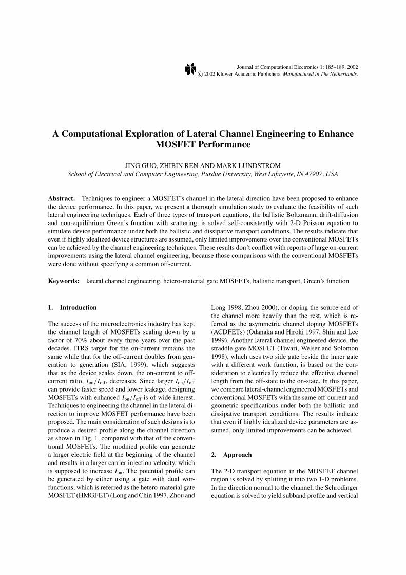
can provide faster speed and lower leakage, designingMOSFETs with enhanced Ion/Ioff is of wide interest.Techniques to engineering the channel in the lateral di-rection to improve MOSFET performance have beenproposed. The main consideration of such designs is toproduce a desired profile along the channel directionas shown in Fig. 1, compared with that of the conven-tional MOSFETs. The modified profile can generatea larger electric field at the beginning of the channeland results in a larger carrier injection velocity, whichis supposed to increase Ion. The potential profile canbe generated by either using a gate with dual wor-functions, which is referred as the hetero-material gateMOSFET (HMGFET) (Long and Chin 1997, Zhou and
Long 1998, Zhou 2000), or doping the source end ofthe channel more heavily than the rest, which is re-ferred as the asymmetric channel doping MOSFETs(ACDFETs) (Odanaka and Hiroki 1997, Shin and Lee1999). Another lateral channel engineered device, thestraddle gate MOSFET (Tiwari, Welser and Solomon1998), which uses two side gate beside the inner gatewith a different work function, is based on the con-sideration to electrically reduce the effective channellength from the off-state to the on-state. In this paper,we compare lateral-channel engineered MOSFETs andconventional MOSFETs with the same off-current andgeometric specifications under both the ballistic anddissipative transport conditions. The results indicatethat even if highly idealized device parameters are as-sumed, only limited improvements can be achieved.
2. Approach
The 2-D transport equation in the MOSFET channelregion is solved by splitting it into two 1-D problems.In the direction normal to the channel, the Schrodingerequation is solved to yield subband profile and vertical
186 Guo
Figure 1. The conventional (solid line) and desired (dashed line)potential profile along the lateral direction of the channel. Also shownis the schematic structure of HMGFETs which can generate the de-sired potential profile if the source gate workfunction φ1 is lager thanthe drain gate workfunction φ2.
electron concentration. In the lateral direction, threetypes of transport equations, the Boltzmann equationin the ballistic limit, drift-diffusion equation and Non-Equilibrium Green’s Function (NEGF) with scatteringare solved to yield electron density in the lateral di-rection and the source-drain current on the basis ofthe subband profiles. A 2D Poisson equation is solvedself-consistently with each of the transport equations.Details of calculation scheme can be found in Taur andNing (1998).
The ballistic limit is calculated semiclassically bysolving Boltzmann equation. For each spatial point, theoccupation of a state in k-space is determined by theFermi-Dirac function with the source or drain Fermilevel, depending on which contact the electrons fillsuch state come from. For example, at the barrier top,the positive half of k-space is filled by electrons fromthe source while the negative half by electrons from thedrain.
In our Green’s function method, we treat scatteringusing a simple Buttiker-probe model. Scattering cen-ters are viewed as reservoirs similar to the source anddrain. However, they differ from the source and drainreservoirs as they can only change the energy of carriersand not the total number of carriers in the system. Thismodel has been demonstrated to capture the essentialphysics of scattering (Taur and Ning 1998).
3. Results and Discussions
The characteristics of a conventional double-gateMOSFET at 30-nm channel length, as shown inFig. 2(a), are calculated as the comparison baseline to
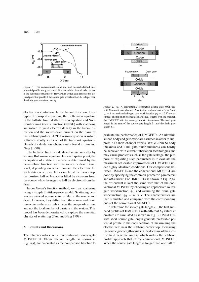
Figure 2. (a) A conventional symmetric double-gate MOSFETwith 30-nm intrinsic channel. An ultrathin body and oxide tsi = 2 nm,tox = 1 nm and a middle gap gate workfunction φG = 4.3 V are as-sumed. The top and bottom gates have equal lengths with the channel.(b) HMGFET with the same geometric dimensions. The total gatelength is the sum of the source gate length L1 and the drain gatelength L2.
evaluate the performance of HMGFETs. An ultrathinsilicon body and gate oxide are assumed in order to sup-press 2-D short channel effects. While 2 nm Si bodythickness and 1 nm gate oxide thickness can hardlybe achieved with current fabrication technologies andmay cause problems such as the gate leakage, the pur-pose of exploiting such parameters is to evaluate themaximum achievable improvement of HMGFETs un-der highly idealized conditions. Our comparisons be-tween HMGFETs and the conventional MOSFET aredone by specifying the common geometric parametersand off-current. For HMGFETs as shown in Fig. 2(b),the off-current is kept the same with that of the con-ventional MOSFET by choosing an appropriate sourcegate workfunction, φ1, and assuming the drain gateworkfunction, φ2 = 4.05 V. The characteristics arethen simulated and compared with the correspondingones of the conventional MOSFET.
To determine the source gate length L1, the first sub-band profiles of HMGFETs with different L1 values aton-state are simulated as shown in Fig. 3. HMGFETswith short source gate length generate preferable po-tential profile in the consideration of maximizing theelectric field near the subband barrier top. Increasingthe source gate length results in the decrease of the elec-tric field near the source, which makes the subbandprofile approach that of the conventional MOSFET.When the source gate length is longer than one half of
Computational Exploration of Lateral Channel Engineering 187
Figure 3. The potential profile along channel at the on-state forHMGFETS with different L1. φ1 = 4.4 V and φ2 = 4.05 V are keptconstant.
Figure 4. The IDS vs. VGS characteristics at VD = 0.6 V calcu-lated by the ballistic transport model. Solid line: the conventionalMOSFET shown in Fig. 2. Dash line: L1 = 5 nm HMGFET withφ1 = 4.46 V. Dot line: L1 = 10 nm HMGFET with φ1 = 4.33 V.Dash-dot line: L1 = 15 nm HMGFET with φ1 = 4.31 V.
the total gate length, the subband profile near the bar-rier top is almost the same as that of the conventionalMOSFET. HMGFETs with three different source gatelengths L1 = 5 nm, 10 nm and 15 nm are studiedin the subsequent ballistic and dissipative transportcalculations.
Figure 4(a) shows IDS-VGS characteristics ofHMGFETs, compared with that of the conventionalMOSFET. The L1 = 5 nm HMGFET has a largersubthreshold swing and worse short-channel immu-nity. Increasing the source gate length to 10 and15 nm improves the subthreshold characteristics, whichare mainly dominated by the device electrostatics.The degraded electrostatic properties associated withHMGFETs can be understood by qualitatively analyz-ing 2-D Poisson equation in the channel region. Theslope of subband profile of HMGFETs increases fromzero at the barrier top to a large value in order to in-crease carrier injection velocity, indicating a rapidlyspatial change of electric field at the position. The
Table 1. On-current evaluation of three HMGFETs using differenttransport models, where the units of Ion are µA/µm and Increase in-dicates the percentage increase of Ion over the conventional MOSFETwith the same transport model.
Ballistic DD NEGF
Increase Increase IncreaseIon (%) Ion (%) Ion (%)
Conventional 2340 – 810 – 1378 –
L1 = 5 nm HMG 1439 −38 605 −25 1248 −10
L1 = 10 nm 2060 −12 829 +2 1615 +17
L1 = 15 nm 2262 −3 882 +10 1643 +20
rapidly varying field results in the large absolute valueof the second derivative of the potential along the chan-nel, which may invalidate the gradual channel approx-imation and lead to more severe 2-D short channeleffects (Ren 2001). Such short channel effects causeless effective gate modulation on the barrier top ofHMGFETs, especially for those HMGFETs with shortsource gate length. Thus the barrier top of HMGFETscannot be pushed down so much as that of the conven-tional MOSFET from the off-state to the on-state. Thehigher subband barrier tops result in the reduction ofthe ballistic on-current as indicated in Table 1.
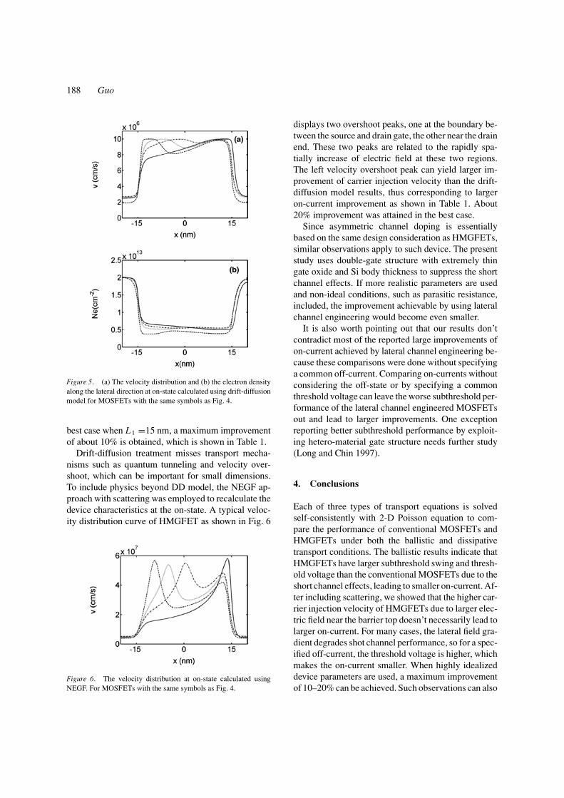
In the presence of scattering, the characteristics ofHMGFETs and the conventional MOSFET are first cal-culated using the drift-diffusion model. From the de-sign consideration of the lateral channel engineering, itmight be expected that the largest Ion improvement canbe achieved by L1 = 5 nm HMGFET because it max-imize the electric field near the barrier top. However,the results indicate an opposite situation as shown inTable 1. Although the L1 = 5 nm HMGFET do achievethe largest carrier injection velocity Vinj as shown inFig. 5(a), the injection carrier density reduction, whichis shown in Fig. 5(b) is more dominant and causes theoverall decrease of the on-current. Such reduction canbe explained on the basis of simple gate control elec-trostatics, which express the injection carrier density asQinj = Ceff (VG − VT ), where Ceff is the effective gatecapacitance, VG is the gate voltage and VT is the thresh-old voltage. The worse subthreshold characteristics ofL1 = 5 nm HMGFET requires a larger VT to yield thespecified off-current, thus causing the decrease of Qinj
at on-state when the same Ceff is assumed. Increasingthe source gate length can lead to larger Qinj, however,at the same time, it decreases Vinj as shown in Fig. 5.This trade-off relation between Qinj and Vinj makes ithard to achieve large on-current improvement. In the
188 Guo
Figure 5. (a) The velocity distribution and (b) the electron densityalong the lateral direction at on-state calculated using drift-diffusionmodel for MOSFETs with the same symbols as Fig. 4.
best case when L1 =15 nm, a maximum improvementof about 10% is obtained, which is shown in Table 1.
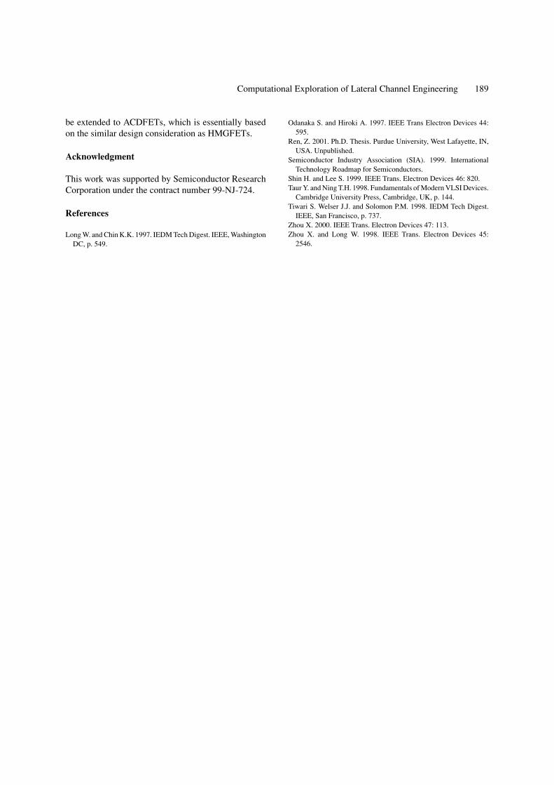
Drift-diffusion treatment misses transport mecha-nisms such as quantum tunneling and velocity over-shoot, which can be important for small dimensions.To include physics beyond DD model, the NEGF ap-proach with scattering was employed to recalculate thedevice characteristics at the on-state. A typical veloc-ity distribution curve of HMGFET as shown in Fig. 6
Figure 6. The velocity distribution at on-state calculated usingNEGF. For MOSFETs with the same symbols as Fig. 4.
displays two overshoot peaks, one at the boundary be-tween the source and drain gate, the other near the drainend. These two peaks are related to the rapidly spa-tially increase of electric field at these two regions.The left velocity overshoot peak can yield larger im-provement of carrier injection velocity than the drift-diffusion model results, thus corresponding to largeron-current improvement as shown in Table 1. About20% improvement was attained in the best case.
Since asymmetric channel doping is essentiallybased on the same design consideration as HMGFETs,similar observations apply to such device. The presentstudy uses double-gate structure with extremely thingate oxide and Si body thickness to suppress the shortchannel effects. If more realistic parameters are usedand non-ideal conditions, such as parasitic resistance,included, the improvement achievable by using lateralchannel engineering would become even smaller.
It is also worth pointing out that our results don’tcontradict most of the reported large improvements ofon-current achieved by lateral channel engineering be-cause these comparisons were done without specifyinga common off-current. Comparing on-currents withoutconsidering the off-state or by specifying a commonthreshold voltage can leave the worse subthreshold per-formance of the lateral channel engineered MOSFETsout and lead to larger improvements. One exceptionreporting better subthreshold performance by exploit-ing hetero-material gate structure needs further study(Long and Chin 1997).
4. Conclusions
Each of three types of transport equations is solvedself-consistently with 2-D Poisson equation to com-pare the performance of conventional MOSFETs andHMGFETs under both the ballistic and dissipativetransport conditions. The ballistic results indicate thatHMGFETs have larger subthreshold swing and thresh-old voltage than the conventional MOSFETs due to theshort channel effects, leading to smaller on-current. Af-ter including scattering, we showed that the higher car-rier injection velocity of HMGFETs due to larger elec-tric field near the barrier top doesn’t necessarily lead tolarger on-current. For many cases, the lateral field gra-dient degrades shot channel performance, so for a spec-ified off-current, the threshold voltage is higher, whichmakes the on-current smaller. When highly idealizeddevice parameters are used, a maximum improvementof 10–20% can be achieved. Such observations can also
Computational Exploration of Lateral Channel Engineering 189
be extended to ACDFETs, which is essentially basedon the similar design consideration as HMGFETs.
Acknowledgment
This work was supported by Semiconductor ResearchCorporation under the contract number 99-NJ-724.
References
Long W. and Chin K.K. 1997. IEDM Tech Digest. IEEE, WashingtonDC, p. 549.
Odanaka S. and Hiroki A. 1997. IEEE Trans Electron Devices 44:595.
Ren, Z. 2001. Ph.D. Thesis. Purdue University, West Lafayette, IN,USA. Unpublished.
Semiconductor Industry Association (SIA). 1999. InternationalTechnology Roadmap for Semiconductors.
Shin H. and Lee S. 1999. IEEE Trans. Electron Devices 46: 820.Taur Y. and Ning T.H. 1998. Fundamentals of Modern VLSI Devices.
Cambridge University Press, Cambridge, UK, p. 144.Tiwari S. Welser J.J. and Solomon P.M. 1998. IEDM Tech Digest.
IEEE, San Francisco, p. 737.Zhou X. 2000. IEEE Trans. Electron Devices 47: 113.Zhou X. and Long W. 1998. IEEE Trans. Electron Devices 45:
2546.