Embed Size (px)
Citation preview

4.2.1EOS/ESD SYMPOSIUM 95-175
A Comparison of Electrostatic Discharge Models and Failure Signaturesfor CMOS Integrated Circuit Devices
M. KellyDelco Electronics Corporation
1800 E. Lincoln Road, M/S R117Kokomo, Indiana 46904-9005
(317) 451-7084
T. DiepAT&T Bell Laboratories
Engineering Research CenterP.O. Box 900
Princeton, New Jersey 08542(609) 639-2412
S. TwerefourFord Microelectronics, Inc.
9965 Federal DriveColorado Springs, Colorado 80921
(719) 528-7709
G. ServaisDelco Electronics Corporation
1800 E. Lincoln Road, M/S R117Kokomo, Indiana 46904-9005
(317) 451-7923
D. LinAT&T Bell Laboratories
Engineering Research CenterP.O. Box 900
Princeton, New Jersey 08542(609) 639-2414
G. ShahFord Motor Company, ACD, Electronics Operations
17000 Rotunda Drive, Room C160Dearborn, Michigan 48121
(313) 845-3599
ABSTRACT
Six different CMOS device codes were evaluated,according to available test standards, for ElectrostaticDischarge (ESD) sensitivity using three ESD models:
• Human Body Model (HBM)• Machine Model (MM)• Field-Induced Charged Device Model (FCDM)
Four commercially available simulators were used: two toperform the HBM ESD evaluations and two to perform the MMESD evaluations. FCDM stressing was performed using anAT&T designed simulator. All stressing was performed atAT&T Bell Laboratories, Delco Electronics, and FordMicroelectronics. The failure threshold voltage and failuresignature associated with each ESD model and simulator weredetermined for each test sample. Threshold correlation andregression analyses were also performed.
Though the three ESD models and simulators createdmultiple failure signatures, they do not exhibit a high degree ofoverlap. Our results will show a high correlation between theESD thresholds, failing pins, failing circuitry, and failingstructures for HBM and MM stressing of the device codesevaluated.
INTRODUCTION
Over the past several years, ESD models haveproliferated as Integrated Circuit (IC) users and manufacturersendeavor to predict IC performance in applicationenvironments. The test techniques being implemented havegrown more complex as a myriad of test-pin combinations
have been specified to guarantee device performance duringproduction and field use. These complex requirements haveresulted in: difficulty measuring ESD sensitivity; a need forlarge sample sizes; an uncertainty when correlating differentsimulators or facilities; and, because ESD stressing isconsidered a destructive test, a significant increase in cost ofqualification.
Several papers have been published in the past few yearsexploring potential correlation between HBM / MM [1,2] andHBM / CDM [3,4,5]. However, an overall comparison of thethree ESD models and the corresponding failure signatures forvarious CMOS technologies has not been reported to date.
In addition, the ESD sensitivity comparisons of previousinvestigations [1,2,3,4] were conducted to evaluate the effectof individual pin combinations or utilized a threshold definitionof the 50% value for the cumulative probability plot. Theseprocedures are not a representation of procedures followed byqualification engineers. The majority of qualification engineersdetermine test failures according to the failure criteriadefinition specified in industry test specifications. We haveinvestigated the correlation between several ESD models fromthe practical standpoint of an individual tasked with performingan ESD qualification test. However, to assess the robustnessof our analysis, we have also performed two additional sets ofcorrelation analysis utilizing a 50% value and a first-fail value.In later sections of this paper, these results will be discussedshowing that the correlation “big picture” is robust.
This paper discusses the results of a round-robin ESDexperiment performed jointly by AT&T Bell Laboratories, DelcoElectronics, and Ford Microelectronics. To minimize thenumber of ESD models required to provide a reasonablyaccurate prediction on the ESD susceptibility of an integrated

4.2.2EOS/ESD SYMPOSIUM 95-176
circuit, the investigation examined the correlation betweenthree ESD models used by the electronics industry: HumanBody Model (HBM), Machine Model (MM), and Field-InducedCharged Device Model (FCDM). The designed experimentcontained two independent variables:
i) Two different test systems performed HBM and MMstressing and one test system performed FCDMstressing.
ii) A total of six different CMOS devices were evaluated,with each participating company providing two devicecodes.
The testing approach attempted to quantify the failingESD voltage level for each ESD model through execution oftesting procedures defined in commonly used test standards.Once all ESD stressing was completed, resulting failuresignatures and failure locations were identified. Optical andScanning Electron Microscope (SEM) photographs areincluded to illustrate typical failure characteristics for eachESD model. The observed physical characteristics of theHBM, MM, and FCDM failures at various voltage levelsprovide a valuable reference tool for the failure analyst taskedwith classifying a transient event resulting in ESD failure.
SELECTION OF TEST SAMPLES
To represent as many component CMOS technologiesand packaging configurations as possible, each participatingcompany provided two device codes of various pin counts forcomplete ESD characterization. Table 1 lists the deviceschosen for the evaluation and the corresponding technology,packaging configuration, and functional description. Thesedevices represent components used in the “real world.”
Table 1: Devices used in round-robin experiment
Device PackageType
Technology Description
X1 44 PLCC 0.9 µm3 volt / 5 volt CMOS
Echo cancellor
X2 100 EIAJ 0.9 µm5 volt CMOS
ASIC for diskdrive system
X3 40 PDIP 1.5 µm5 volt CMOS
Audioapplications
X4 28 PLCC 1.5 µm5 volt CMOS
Bus interface forcommunication
and data
X5 28 PDIP 1.2 µm5 volt CMOS
Controls modulecommunications
for vehicle
X6 24 PDIP 1.5 µm5 volt CMOS
2K x 8 bit staticRAM
TEST EQUIPMENT AND PROCEDURE
The Human Body Model is designed to simulate a humanbody discharging accumulated static charge (via a fingertip)through a device to ground (see Fig. 1). It comprises a seriesRC network of a 100 pF capacitor and a 1500 Ω resistor [6,7].
I
Time (ns)
t
Cur
rent
(Am
ps)
0 100ns
0.33
0
Figure 1: 500 volt HBM ESD discharge waveform through ashort (for waveform details, see [6,7]).
The Machine Model is designed to simulate a machine(test equipment, furniture, etc.) discharging accumulated staticcharge through a device to ground (see Fig. 2). It comprises aseries RC network of a 200 pF capacitor, a resistor ofapproximately 8.5 Ω, and an inductor of approximately 0.5 µH[8].
Time (ns)t
I
Cur
rent
(Am
ps)
0 100ns
8.75
0
Figure 2: 500 volt MM ESD discharge waveform through ashort (for waveform details, see [8]).
The Charged Device Model, on the other hand, simulatesa charged device (e.g., sliding down a shipping tube, etc.)discharging directly to ground (see Fig. 3) [9,10,11].

4.2.3EOS/ESD SYMPOSIUM 95-177
Time (ns)
IC
urre
nt (
Am
ps)
t0 5ns
0
4.5
Figure 3: 500 volt FCDM ESD discharge waveform using a4 pF module (for waveform details, see [11]).
All Human Body Model (HBM) and Machine Model (MM)ESD stressing was performed using two different commerciallyavailable ESD simulators and Field-Induced Charged DeviceModel (FCDM) ESD stressing was performed using an AT&Tdesigned simulator [12,13]. To insure proper simulation andrepeatable ESD results, simulator waveform performance wasverified following the procedure outlined in the ESDAssociation HBM and MM ESD specifications [6,8] and theJEDEC FCDM ESD specification [11]. Based upon familiaritywith the CDM event and characterization procedure, AT&T BellLaboratories performed all FCDM stressing. FordMicroelectronics and Delco Electronics, both automotiveelectronics users and manufacturers, performed all HBM andMM ESD stressing.
Prior to ESD characterizations, complete DC parametricand functional testing per applicable device specificationrequirements was performed on all test samples. For HBMand MM stressing, all pins on each device were subjected toESD stressing with three positive and three negative pulseswith a one second delay between each pulse. Devicestressing was accomplished following the pin combinationcriteria outlined in the ESD Association HBM and MM ESDspecifications [6,8]. For FCDM stressing, each pin wasstressed with three positive and three negative pulses with atleast 0.1 second delay between pulses, following theprocedure outlined in the JEDEC FCDM ESD specification[11].
The stress voltage levels for each ESD model wereselected based on prior experience with the devices and areshown in Table 2. For devices X1 and X2, a step-stressprocedure was used on a sample of three available devicesper device code. For devices X3 through X6, a new sample ofthree devices was used at each stress voltage level to avoidany cumulative effect due to the ESD stressing itself [14]. Atotal of 933 devices were stressed for this study. Once thestressing was completed, all devices were returned to theoriginating company for complete DC parametric andfunctional testing per applicable device specificationrequirements. Devices failing the electrical testing criteriawere then submitted for failure analysis.
ELECTRICAL RESULTS
To insure an accurate evaluation, all experimental deviceswere functionally tested at each location before and afterbeing subjected to ESD stress. For devices X1 and X2, a 30%shift in I/V curve trace characteristics was used as the failurecriteria. For devices X3 through X6, the failure criteria was achange in device functionality or leakage current exceedingthe applicable device specification requirements, as specifiedin the industry ESD test specifications (ESD Association HBM,ESD Association MM, and JEDEC FCDM). The results ofthese tests were then used to determine the ESD threshold foreach device code.
The results for the ESD stressing of all devices aresummarized in Table 3. The summaries detail the failurethreshold voltage levels and packaging configurations. Allfailure threshold voltage levels are listed as the last passingvoltage level, P, and first failing voltage level, F, whenapplicable. If an entry lists only one threshold, either P or F,the testing procedure was unable to fully characterize theparticular device. For devices without a passing voltage level,a value of zero volts was used as the default passing voltagelevel. Initial stressing of device X3 began at 6000 volts.However, further characterization revealed the failurethreshold to be less than 6000 volts. Additional stressing wasperformed at lower stress voltage levels (3000 V, 4000 V, and5000 V). Due to a limited number of available samples andtime constraints, only Delco was able to complete a fullcharacterization at the lower stress voltage levels (asindicated in Table 3).
Table 2: Device Stress Voltage Levels
Device HBM (V) MM (V) FCDM (V)
X1 500 to failure,steps of 500
50 to failure,steps of 50
200, 500, 1000
X2 500 to failure,steps of 500
50 to failure,steps of 50
200, 500, 1000,1500, 2000
X3 3000, 4000,5000, 6000
200, 300, 400,500
200, 500, 1000,1500, 2000
X4 1000, 1500,2000
100, 150, 200 200, 500, 1000,1500, 2000
X5 1000, 1500,2000, 2500,3000
100, 150, 200,250, 300
200, 500, 1000,1500, 2000
X6 2500, 3000,3500, 4000,4500, 5000,5500, 6000
100, 150, 200,250, 300
200, 500, 1000,1500, 2000
4.2.4EOS/ESD SYMPOSIUM 95-178
Table 3: Results for HBM, MM, and FCDM ESD Stressing
Test PackageHBM ESD (V) MM ESD (V) FCDM ESD (V)
Sample TypeDelco Stressing Ford Stressing Delco Stressing Ford Stressing AT&T Stressing
X1 44 PLCC default (0) / F 500 default (0) / F 500 F 50 P 50 / F 100 P 500 / F 1000
X2 100 EIAJ P 1000 / F 1500 P 1000 / F 1500 P 50 / F 100 P 100 / F 150 P 2000
X3 40 PDIP P 3000 / F 4000 F 6000 P 300 / F 400 F 400 P 500 / F 1000
X4 28 PLCC P 1000 / F 1500 P 1000 / F 1500 P 100 / F 150 F 100 P 500 / F 1000
X5 28 PDIP P 2000 / F 2500 P 2000 / F 2500 P 200 / F 250 P 200 / F 250 P 500 / F 1000
X6 24 PDIP P 4000 / F 4500 P 4000 / F 4500 P 300 P 250 / F 300 P 500 / F 1000
Since the device stress voltage levels shown in Table 2involved relatively large voltage increments (500 volts forHBM, 50 volts for MM, and 500 volts for FCDM), a failurethreshold needed to be established for later correlationanalysis. Based upon the stressing results for each ESDmodel (as shown in Table 3), a “best estimate” of failurethreshold for each device was determined. These bestestimate threshold values are shown in Table 4.
For HBM and MM stress results (devices stressed at twodifferent locations), this “best estimate” was accomplished foreach device by calculating the midpoint between the lowerpassing stress voltage level (identified with a P) and the lowerfailing stress voltage level (identified with a F). For example,device X1 lists MM stress results of 50 volts (Fail) for Delcostressing and 50 volts (Pass), 100 volts (Fail) for Fordstressing. The values used to determine the “best estimate” offailure threshold would then be 50 volts (Pass) and 50 volts(Fail), resulting in a best estimate value threshold of 50 volts.
For FCDM stress results, this “best estimate” wasaccomplished for each device by calculating the midpointbetween the passing stress voltage level (identified with a P)and the failing stress voltage level (identified with an F).Device X2, with a passing stress voltage level equal to theFCDM stress limit, was assigned a “best estimate” threshold ofthe value listed in Table 3 (2000 volts).
Our method for determining the best estimate of the ESDfailure threshold is a simple linear interpolation between adevice’s “pass” and “fail” voltage levels. Other methods ofdetermining a failure threshold estimate exist. We will discusstwo additional methods in a later section of this paper for thepurpose of examining the robustness of our correlationanalysis.
Table 4: “Best Estimate” Failure Thresholds
Device HBM ESD(V)
MM ESD(V)
FCDM ESD(V)
X1 250 50 750
X2 1250 75 2000
X3 3500 350 750
X4 1250 100 750
X5 2250 225 750
X6 4250 275 750
FAILURE ANALYSIS PROCEDURE
Once all experimental devices had been functionallytested, the devices failing the electrical testing acceptancecriteria were submitted for failure analysis. Each device’sfailure location and signature were determined anddocumented for each ESD model.
The failure analysis techniques used by each participatingcompany were universal and tend to follow the samestructured flow [15]. First, the failure was verified usingmicroscopes, curve tracing equipment, and automated testequipment (ATE). The failing component was thendecapsulated and examined using optical microscopy,emission microscopy, and liquid crystal techniques.
When the failure could not be easily located, circuitanalysis and fault isolation procedures were required; thisnormally involved the utilization of a microprobe station,Electron-beam test system (E-beam), or ion mill (Focused IonBeam). Once the failure site was identified, subsurface
4.2.5EOS/ESD SYMPOSIUM 95-179
analysis was required to further reveal the damage location.These techniques included cross-sectioning and ScanningElectron Microscopy (SEM). The failure signature was thendocumented and photographed.
FAILURE MODE ANALYSIS RESULTS AND DISCUSSION
Failure mode analysis procedures were aimed atestablishing a physical signature associated with electricalfailure of a device at the ESD threshold. All results aresummarized in Table 5.
Nomarksi phase contrast and scanning electronmicroscopy (SEM) were performed on a number of ESDdamaged devices. Failure analysis revealed the failuresignatures to be consistent with classical ESD failuresignatures:
• Gate oxide damage• Poly-filament & Poly-extrusion• Metal melt filament through a junction• Contact spiking• Metal burn-out
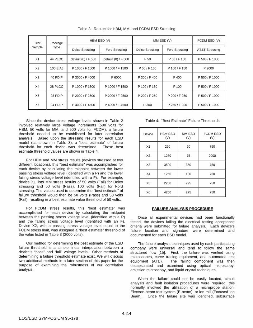
SEM examinations revealed that two HBM simulatorsperforming ESD stressing at the same stress voltage level canproduce different failure signatures for the same device [16](see Figures 4 and 5). In addition, device X5 results indicatethat the three ESD models produced three different failuresignatures as shown in Figures 4 through 7.
Figure 4: Device X5; Delco stressing; HBM ESD failuresignature showing poly-extrusion damage of an I/O pinprotection circuitry NMOS transistor. Poly-extrusion damageresulted in shorting of the gate to drain.
Figure 5: Device X5; Ford stressing; HBM ESD failuresignature showing gate oxide damage of an internal NMOStransistor.
Figure 6: Device X5; Delco and Ford stressing; MM ESDfailure signature showing metal melt damage of an NMOStransistor located in the ESD protection circuitry.
Figure 7: Device X5; AT&T stressing; FCDM ESD failuresignature showing gate oxide and poly-filament damage of aninternal PMOS transistor.
4.2.6EOS/ESD SYMPOSIUM 95-180
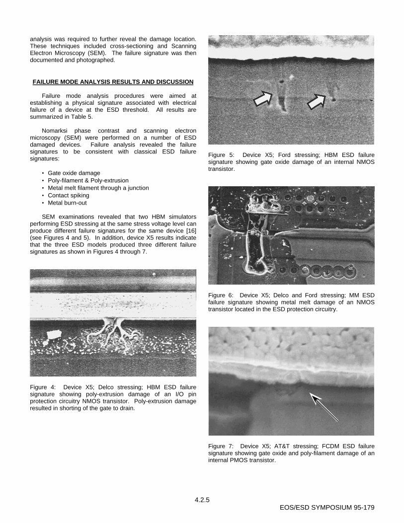
Examination of failure analysis results for device X4 alsoindicates that a single failure signature (e.g., gate oxidedamage) can be produced by all three ESD models on thesame device (see Figures 8, 9, and 10).
Figure 8: Device X4; Delco and Ford stressing; HBM ESDfailure signature showing gate oxide damage of an internalNMOS transistor.
Figure 9: Device X4; Delco and Ford stressing; MM ESDfailure signature showing gate oxide damage of an internalPMOS transistor.
Figure 10: Device X4; AT&T stressing; FCDM ESD failuresignature showing gate oxide damage of an internal NMOStransistor.
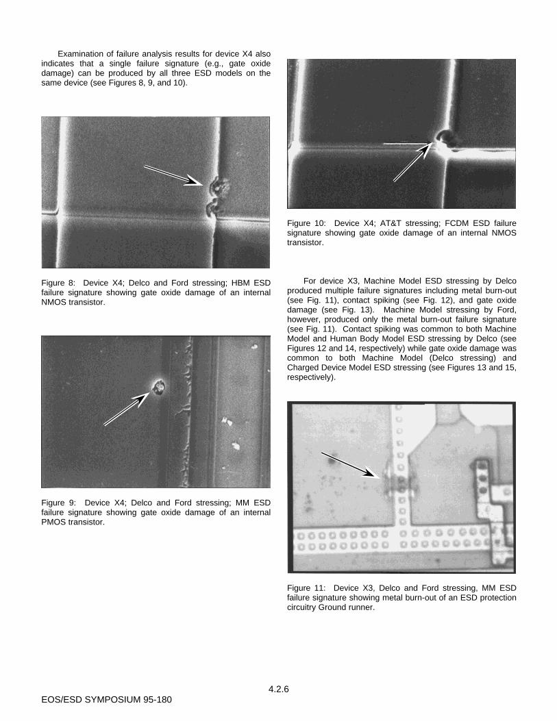
For device X3, Machine Model ESD stressing by Delcoproduced multiple failure signatures including metal burn-out(see Fig. 11), contact spiking (see Fig. 12), and gate oxidedamage (see Fig. 13). Machine Model stressing by Ford,however, produced only the metal burn-out failure signature(see Fig. 11). Contact spiking was common to both MachineModel and Human Body Model ESD stressing by Delco (seeFigures 12 and 14, respectively) while gate oxide damage wascommon to both Machine Model (Delco stressing) andCharged Device Model ESD stressing (see Figures 13 and 15,respectively).
Figure 11: Device X3, Delco and Ford stressing, MM ESDfailure signature showing metal burn-out of an ESD protectioncircuitry Ground runner.
4.2.7EOS/ESD SYMPOSIUM 95-181
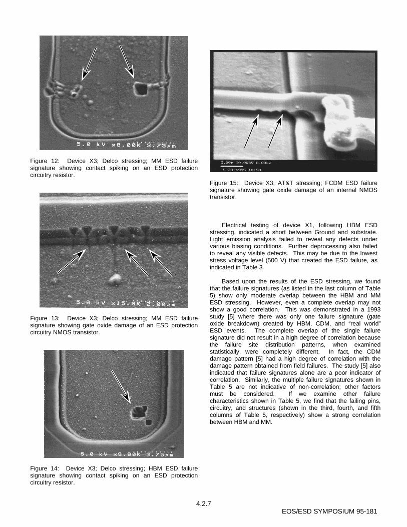
Figure 12: Device X3; Delco stressing; MM ESD failuresignature showing contact spiking on an ESD protectioncircuitry resistor.
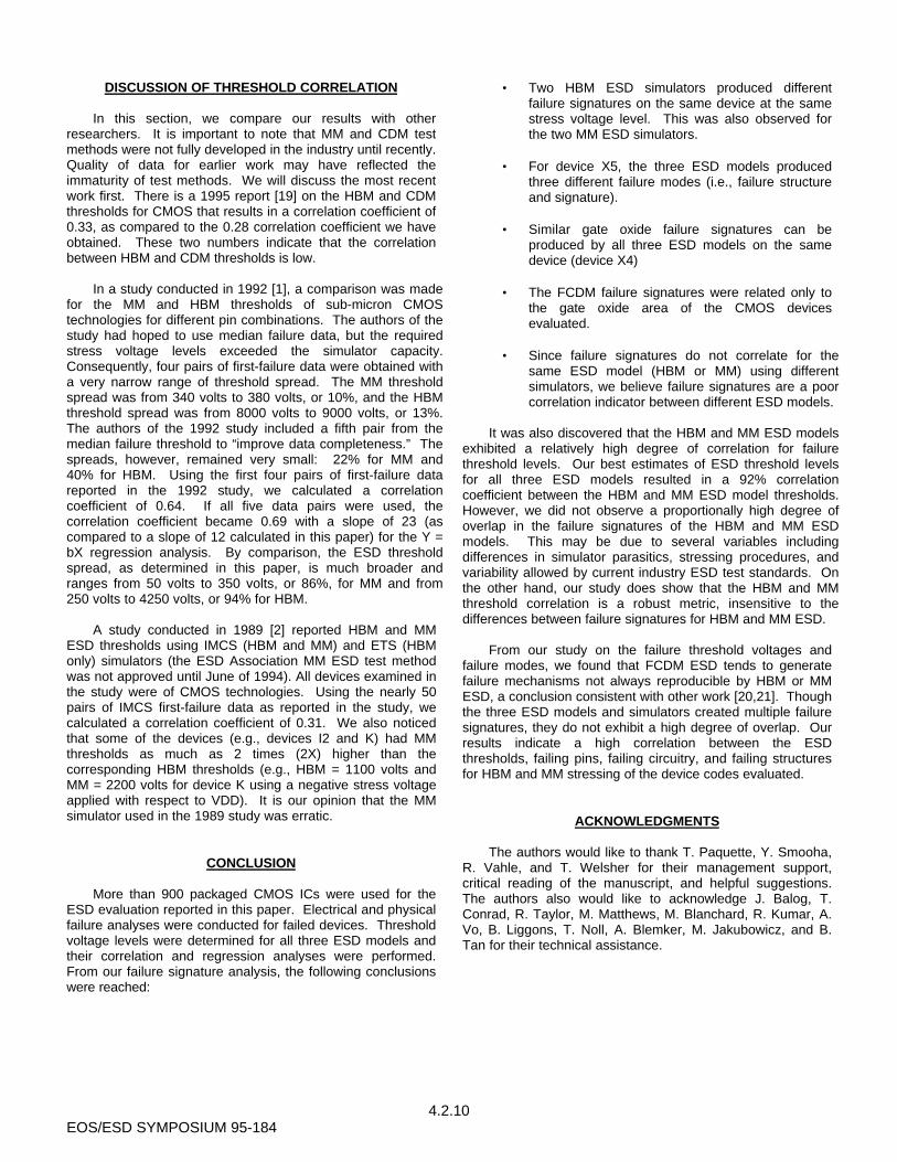
Figure 13: Device X3; Delco stressing; MM ESD failuresignature showing gate oxide damage of an ESD protectioncircuitry NMOS transistor.
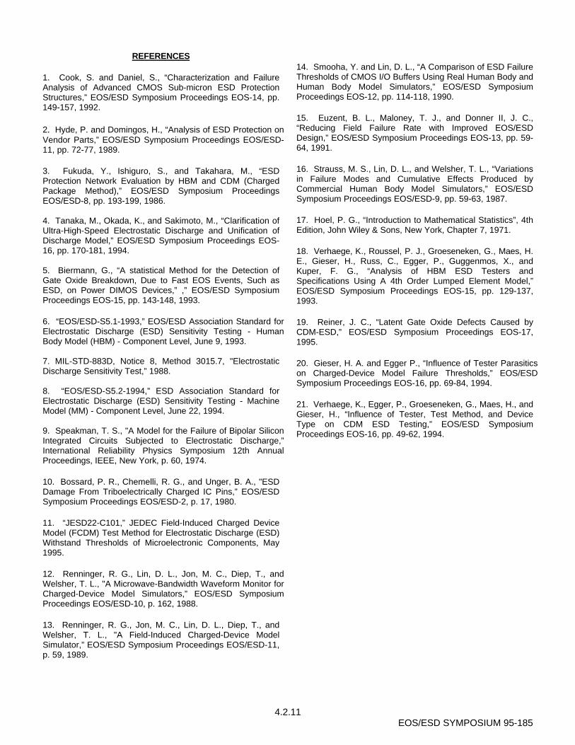
Figure 14: Device X3; Delco stressing; HBM ESD failuresignature showing contact spiking on an ESD protectioncircuitry resistor.
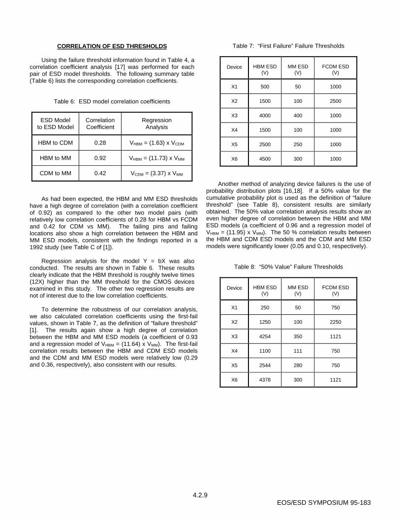
Figure 15: Device X3; AT&T stressing; FCDM ESD failuresignature showing gate oxide damage of an internal NMOStransistor.
Electrical testing of device X1, following HBM ESDstressing, indicated a short between Ground and substrate.Light emission analysis failed to reveal any defects undervarious biasing conditions. Further deprocessing also failedto reveal any visible defects. This may be due to the loweststress voltage level (500 V) that created the ESD failure, asindicated in Table 3.
Based upon the results of the ESD stressing, we foundthat the failure signatures (as listed in the last column of Table5) show only moderate overlap between the HBM and MMESD stressing. However, even a complete overlap may notshow a good correlation. This was demonstrated in a 1993study [5] where there was only one failure signature (gateoxide breakdown) created by HBM, CDM, and “real world”ESD events. The complete overlap of the single failuresignature did not result in a high degree of correlation becausethe failure site distribution patterns, when examinedstatistically, were completely different. In fact, the CDMdamage pattern [5] had a high degree of correlation with thedamage pattern obtained from field failures. The study [5] alsoindicated that failure signatures alone are a poor indicator ofcorrelation. Similarly, the multiple failure signatures shown inTable 5 are not indicative of non-correlation; other factorsmust be considered. If we examine other failurecharacteristics shown in Table 5, we find that the failing pins,circuitry, and structures (shown in the third, fourth, and fifthcolumns of Table 5, respectively) show a strong correlationbetween HBM and MM.

4.2.8EOS/ESD SYMPOSIUM 95-182
Table 5: Device Failure Mode Results
TestSample
ESD Model &Stressing Company
Failing Pin(Input, Output,
Power)
Failing Circuitry(Protection,
Internal)
Failing Structure(PMOS, NMOS, Diode)
FailureSignature
HBM / Delco Output Protection Diode FMA Inconclusive
HBM / Ford Output Protection Diode FMA Inconclusive
X1 MM / Delco Output Protection Diode Junction Damage
MM / Ford Output Protection Diode Junction Damage
FCDM / AT&T VDD Protection PMOS Gate Oxide
HBM / Delco I/O Protection NMOS Gate Oxide
HBM / Ford I/O Protection NMOS Gate Oxide
X2 MM / Delco I/O Protection Diode Junction Damage
MM / Ford I/O Protection Diode Junction Damage
FCDM / AT&T No Fail No Fail No Fail No Fail
HBM / Delco Output Protection Resistor Contact Spiking
HBM / Ford GND Protection GND Runner Metal Burn-out
X3 MM / Delco Input, Output, &GND
Protection GND Runner, Resistor,& NMOS
Metal Burn-out, ContactSpiking, & Gate Oxide
MM / Ford GND Protection GND Runner Metal Burn-out
FCDM / AT&T I/O Internal NMOS Gate Oxide
HBM / Delco I/O & VDD Internal NPN & PMOS Contact Spiking & GateOxide
HBM / Ford Input Internal NMOS Gate Oxide
X4 MM / Delco VDD Internal PMOS Gate Oxide
MM / Ford I/O & VDD Internal PMOS & NMOS Gate Oxide & Contact spike
FCDM / AT&T Input Internal NMOS Gate Oxide
HBM / Delco I/O Protection NMOS Poly-extrusion
HBM / Ford VDD Internal NMOS Gate Oxide
X5 MM / Delco VDD Protection NMOS Metal melt
MM / Ford VDD Protection NMOS Metal melt
FCDM / AT&T VDD Internal PMOS Gate Oxide & Poly-filament
HBM / Delco I/O Protection NMOS Gate Oxide
HBM / Ford I/O Protection NMOS Gate Oxide
X6 MM / Delco No Fail No Fail No Fail No Fail
MM / Ford I/O Protection NMOS & PMOS Metal melt & ContactSpiking
FCDM / AT&T I/O Protection PMOS Gate Oxide & Poly-filament
4.2.9EOS/ESD SYMPOSIUM 95-183
CORRELATION OF ESD THRESHOLDS
Using the failure threshold information found in Table 4, acorrelation coefficient analysis [17] was performed for eachpair of ESD model thresholds. The following summary table(Table 6) lists the corresponding correlation coefficients.
Table 6: ESD model correlation coefficients
ESD Modelto ESD Model
CorrelationCoefficient
RegressionAnalysis
HBM to CDM 0.28 VHBM = (1.63) x VCDM
HBM to MM 0.92 VHBM = (11.73) x VMM
CDM to MM 0.42 VCDM = (3.37) x VMM
As had been expected, the HBM and MM ESD thresholdshave a high degree of correlation (with a correlation coefficientof 0.92) as compared to the other two model pairs (withrelatively low correlation coefficients of 0.28 for HBM vs FCDMand 0.42 for CDM vs MM). The failing pins and failinglocations also show a high correlation between the HBM andMM ESD models, consistent with the findings reported in a1992 study (see Table C of [1]).
Regression analysis for the model Y = bX was alsoconducted. The results are shown in Table 6. These resultsclearly indicate that the HBM threshold is roughly twelve times(12X) higher than the MM threshold for the CMOS devicesexamined in this study. The other two regression results arenot of interest due to the low correlation coefficients.
To determine the robustness of our correlation analysis,we also calculated correlation coefficients using the first-failvalues, shown in Table 7, as the definition of “failure threshold”[1]. The results again show a high degree of correlationbetween the HBM and MM ESD models (a coefficient of 0.93and a regression model of VHBM = (11.64) x VMM). The first-failcorrelation results between the HBM and CDM ESD modelsand the CDM and MM ESD models were relatively low (0.29and 0.36, respectively), also consistent with our results.
Table 7: “First Failure” Failure Thresholds
Device HBM ESD(V)
MM ESD(V)
FCDM ESD(V)
X1 500 50 1000
X2 1500 100 2500
X3 4000 400 1000
X4 1500 100 1000
X5 2500 250 1000
X6 4500 300 1000
Another method of analyzing device failures is the use ofprobability distribution plots [16,18]. If a 50% value for thecumulative probability plot is used as the definition of “failurethreshold” (see Table 8), consistent results are similarlyobtained. The 50% value correlation analysis results show aneven higher degree of correlation between the HBM and MMESD models (a coefficient of 0.96 and a regression model ofVHBM = (11.95) x VMM). The 50 % correlation results betweenthe HBM and CDM ESD models and the CDM and MM ESDmodels were significantly lower (0.05 and 0.10, respectively).
Table 8: “50% Value” Failure Thresholds
Device HBM ESD(V)
MM ESD(V)
FCDM ESD(V)
X1 250 50 750
X2 1250 100 2250
X3 4254 350 1121
X4 1100 111 750
X5 2544 280 750
X6 4378 300 1121
4.2.10EOS/ESD SYMPOSIUM 95-184
DISCUSSION OF THRESHOLD CORRELATION
In this section, we compare our results with otherresearchers. It is important to note that MM and CDM testmethods were not fully developed in the industry until recently.Quality of data for earlier work may have reflected theimmaturity of test methods. We will discuss the most recentwork first. There is a 1995 report [19] on the HBM and CDMthresholds for CMOS that results in a correlation coefficient of0.33, as compared to the 0.28 correlation coefficient we haveobtained. These two numbers indicate that the correlationbetween HBM and CDM thresholds is low.
In a study conducted in 1992 [1], a comparison was madefor the MM and HBM thresholds of sub-micron CMOStechnologies for different pin combinations. The authors of thestudy had hoped to use median failure data, but the requiredstress voltage levels exceeded the simulator capacity.Consequently, four pairs of first-failure data were obtained witha very narrow range of threshold spread. The MM thresholdspread was from 340 volts to 380 volts, or 10%, and the HBMthreshold spread was from 8000 volts to 9000 volts, or 13%.The authors of the 1992 study included a fifth pair from themedian failure threshold to “improve data completeness.” Thespreads, however, remained very small: 22% for MM and40% for HBM. Using the first four pairs of first-failure datareported in the 1992 study, we calculated a correlationcoefficient of 0.64. If all five data pairs were used, thecorrelation coefficient became 0.69 with a slope of 23 (ascompared to a slope of 12 calculated in this paper) for the Y =bX regression analysis. By comparison, the ESD thresholdspread, as determined in this paper, is much broader andranges from 50 volts to 350 volts, or 86%, for MM and from250 volts to 4250 volts, or 94% for HBM.
A study conducted in 1989 [2] reported HBM and MMESD thresholds using IMCS (HBM and MM) and ETS (HBMonly) simulators (the ESD Association MM ESD test methodwas not approved until June of 1994). All devices examined inthe study were of CMOS technologies. Using the nearly 50pairs of IMCS first-failure data as reported in the study, wecalculated a correlation coefficient of 0.31. We also noticedthat some of the devices (e.g., devices I2 and K) had MMthresholds as much as 2 times (2X) higher than thecorresponding HBM thresholds (e.g., HBM = 1100 volts andMM = 2200 volts for device K using a negative stress voltageapplied with respect to VDD). It is our opinion that the MMsimulator used in the 1989 study was erratic.
CONCLUSION
More than 900 packaged CMOS ICs were used for theESD evaluation reported in this paper. Electrical and physicalfailure analyses were conducted for failed devices. Thresholdvoltage levels were determined for all three ESD models andtheir correlation and regression analyses were performed.From our failure signature analysis, the following conclusionswere reached:
• Two HBM ESD simulators produced differentfailure signatures on the same device at the samestress voltage level. This was also observed forthe two MM ESD simulators.
• For device X5, the three ESD models producedthree different failure modes (i.e., failure structureand signature).
• Similar gate oxide failure signatures can beproduced by all three ESD models on the samedevice (device X4)
• The FCDM failure signatures were related only tothe gate oxide area of the CMOS devicesevaluated.
• Since failure signatures do not correlate for thesame ESD model (HBM or MM) using differentsimulators, we believe failure signatures are a poorcorrelation indicator between different ESD models.
It was also discovered that the HBM and MM ESD modelsexhibited a relatively high degree of correlation for failurethreshold levels. Our best estimates of ESD threshold levelsfor all three ESD models resulted in a 92% correlationcoefficient between the HBM and MM ESD model thresholds.However, we did not observe a proportionally high degree ofoverlap in the failure signatures of the HBM and MM ESDmodels. This may be due to several variables includingdifferences in simulator parasitics, stressing procedures, andvariability allowed by current industry ESD test standards. Onthe other hand, our study does show that the HBM and MMthreshold correlation is a robust metric, insensitive to thedifferences between failure signatures for HBM and MM ESD.
From our study on the failure threshold voltages andfailure modes, we found that FCDM ESD tends to generatefailure mechanisms not always reproducible by HBM or MMESD, a conclusion consistent with other work [20,21]. Thoughthe three ESD models and simulators created multiple failuresignatures, they do not exhibit a high degree of overlap. Ourresults indicate a high correlation between the ESDthresholds, failing pins, failing circuitry, and failing structuresfor HBM and MM stressing of the device codes evaluated.
ACKNOWLEDGMENTS
The authors would like to thank T. Paquette, Y. Smooha,R. Vahle, and T. Welsher for their management support,critical reading of the manuscript, and helpful suggestions.The authors also would like to acknowledge J. Balog, T.Conrad, R. Taylor, M. Matthews, M. Blanchard, R. Kumar, A.Vo, B. Liggons, T. Noll, A. Blemker, M. Jakubowicz, and B.Tan for their technical assistance.
4.2.11EOS/ESD SYMPOSIUM 95-185
REFERENCES
1. Cook, S. and Daniel, S., “Characterization and FailureAnalysis of Advanced CMOS Sub-micron ESD ProtectionStructures,” EOS/ESD Symposium Proceedings EOS-14, pp.149-157, 1992.
2. Hyde, P. and Domingos, H., “Analysis of ESD Protection onVendor Parts,” EOS/ESD Symposium Proceedings EOS/ESD-11, pp. 72-77, 1989.
3. Fukuda, Y., Ishiguro, S., and Takahara, M., “ESDProtection Network Evaluation by HBM and CDM (ChargedPackage Method),” EOS/ESD Symposium ProceedingsEOS/ESD-8, pp. 193-199, 1986.
4. Tanaka, M., Okada, K., and Sakimoto, M., “Clarification ofUltra-High-Speed Electrostatic Discharge and Unification ofDischarge Model,” EOS/ESD Symposium Proceedings EOS-16, pp. 170-181, 1994.
5. Biermann, G., “A statistical Method for the Detection ofGate Oxide Breakdown, Due to Fast EOS Events, Such asESD, on Power DIMOS Devices,” ,” EOS/ESD SymposiumProceedings EOS-15, pp. 143-148, 1993.
6. “EOS/ESD-S5.1-1993,” EOS/ESD Association Standard forElectrostatic Discharge (ESD) Sensitivity Testing - HumanBody Model (HBM) - Component Level, June 9, 1993.
7. MIL-STD-883D, Notice 8, Method 3015.7, "ElectrostaticDischarge Sensitivity Test,” 1988.
8. “EOS/ESD-S5.2-1994,” ESD Association Standard forElectrostatic Discharge (ESD) Sensitivity Testing - MachineModel (MM) - Component Level, June 22, 1994.
9. Speakman, T. S., "A Model for the Failure of Bipolar SiliconIntegrated Circuits Subjected to Electrostatic Discharge,”International Reliability Physics Symposium 12th AnnualProceedings, IEEE, New York, p. 60, 1974.
10. Bossard, P. R., Chemelli, R. G., and Unger, B. A., "ESDDamage From Triboelectrically Charged IC Pins,” EOS/ESDSymposium Proceedings EOS/ESD-2, p. 17, 1980.
11. “JESD22-C101,” JEDEC Field-Induced Charged DeviceModel (FCDM) Test Method for Electrostatic Discharge (ESD)Withstand Thresholds of Microelectronic Components, May1995.
12. Renninger, R. G., Lin, D. L., Jon, M. C., Diep, T., andWelsher, T. L., "A Microwave-Bandwidth Waveform Monitor forCharged-Device Model Simulators,” EOS/ESD SymposiumProceedings EOS/ESD-10, p. 162, 1988.
13. Renninger, R. G., Jon, M. C., Lin, D. L., Diep, T., andWelsher, T. L., "A Field-Induced Charged-Device ModelSimulator,” EOS/ESD Symposium Proceedings EOS/ESD-11,p. 59, 1989.
14. Smooha, Y. and Lin, D. L., “A Comparison of ESD FailureThresholds of CMOS I/O Buffers Using Real Human Body andHuman Body Model Simulators,” EOS/ESD SymposiumProceedings EOS-12, pp. 114-118, 1990.
15. Euzent, B. L., Maloney, T. J., and Donner II, J. C.,“Reducing Field Failure Rate with Improved EOS/ESDDesign,” EOS/ESD Symposium Proceedings EOS-13, pp. 59-64, 1991.
16. Strauss, M. S., Lin, D. L., and Welsher, T. L., “Variationsin Failure Modes and Cumulative Effects Produced byCommercial Human Body Model Simulators,” EOS/ESDSymposium Proceedings EOS/ESD-9, pp. 59-63, 1987.
17. Hoel, P. G., “Introduction to Mathematical Statistics”, 4thEdition, John Wiley & Sons, New York, Chapter 7, 1971.
18. Verhaege, K., Roussel, P. J., Groeseneken, G., Maes, H.E., Gieser, H., Russ, C., Egger, P., Guggenmos, X., andKuper, F. G., “Analysis of HBM ESD Testers andSpecifications Using A 4th Order Lumped Element Model,”EOS/ESD Symposium Proceedings EOS-15, pp. 129-137,1993.
19. Reiner, J. C., “Latent Gate Oxide Defects Caused byCDM-ESD,” EOS/ESD Symposium Proceedings EOS-17,1995.
20. Gieser, H. A. and Egger P., “Influence of Tester Parasiticson Charged-Device Model Failure Thresholds,” EOS/ESDSymposium Proceedings EOS-16, pp. 69-84, 1994.
21. Verhaege, K., Egger, P., Groeseneken, G., Maes, H., andGieser, H., “Influence of Tester, Test Method, and DeviceType on CDM ESD Testing,” EOS/ESD SymposiumProceedings EOS-16, pp. 49-62, 1994.