Embed Size (px)
Citation preview

A CAPACITOR-LESS WIDE-BAND POWER SUPPLY REJECTION
LOW DROP-OUT VOLTAGE REGULATOR WITH CAPACITANCE MULTIPLIER
A Thesis
by
MENGDE WANG
Submitted to the Office of Graduate and Professional Studies of
Texas A&M University
in partial fulfillment of the requirements for the degree of
MASTER OF SCIENCE
Chair of Committee, Edgar Sanchez-Sinencio
Committee Members, Kamran Entesari
Peng Li
Alexander Parlos
Head of Department, Chanan Singh
August 2014
Major Subject: Electrical Engineering
Copyright 2014 Mengde Wang

ii
ABSTRACT
A Low Drop-Out (LDO) voltage regulator with both capacitor-less and high
power supply rejection (PSR) bandwidth attributes is highly admired for an integrated
power management system of mobile electronics. The capacitor-less feature is demanded
for realizing more compact device. The high PSR bandwidth is essential for being used
with high frequency switching regulators. These two attributes are of strong trade-off
because usually a capacitor-less LDO requires Miller Compensation which greatly limits
the PSR bandwidth.
This thesis presents a LDO design with both capacitor-less and high PSR
bandwidth attributes. The proposed LDO structure incorporates external compensation
which is gifted for extended PSR bandwidth. A capacitance multiplier (CM) of high
multiplication factor (≈ 100) is designed to externally compensate the LDO without an
external off-chip capacitor. In the proposed LDO circuit, NMOS is used as the pass
transistor for system stabilization. Triple-well NMOS and Zero-Vt NMOS are used as
pass transistors in the two main LDO designs. The design with the triple-well NMOS
pass transistor aims at higher PSR bandwidth with lower power consumption. The
design with Zero-Vt NMOS pass transistor eliminates the necessity of a charge pump for
driving the gate of a NMOS pass transistor.
Implemented in IBM 0.18µm technology, the LDO with triple-well NMOS
achieves -40dB PSR to 19MHz with 265µA current consumption. The LDO with Zero-
Vt NMOS achieves -40dB PSR to 10MHz with 350µA current consumption. In this

iii
design, the feasibility of using Zero-Vt NMOS as a LDO pass transistor is proved.
Moreover, compared to traditional capacitor-less LDOs with PSR bandwidth around
10kHz and above 0dB PSR beyond 10MHz, the PSR bandwidth of the proposed LDO
structure is greatly extended with significant PSR over 10MHz. This also proves the
feasibility of applying external compensation strategy to a capacitor-less LDO and its
great beneficial effect on the PSR of the LDO.

iv
DEDICATION
To my faith to have a happy family and to be a good engineer.

v
ACKNOWLEDGEMENTS
I would like to first thank my advisor, Dr. Edgar Sanchez-Sinencio for his expert
knowledge and guidance throughout my entire Master’s program at Texas A&M
University. I also would like to thank Dr. Entesari, Li and Parlos for serving as my
committee member. I would like to thank my colleague, Jorge Zarate-Roldan for his
very helpful and patient discussion with we throughout this project. I also would like to
thank my peers, namely Joselyn Torress, Mohammed Abouzied, Salvador Carreon,
Fernando Lavalle, Adrian Coli, Jiayi Jin, Xiaosen Liu, Congyin Shi, Kyoohyun Noh,
Alexander Kartono for their warm-hearted technical input and moral support.
I would like to thank my parents for their unconditional and unreserved love
throughout my life. I would like to thank my mother for her encouragement to help me
get through desperation. I would like to thank my father for sharing his experience with
me. I also would like to thank my girlfriend for her sincere accompany with me through
my graduate study, which bring colors to my life.
vi
TABLE OF CONTENTS
Page
ABSTRACT .......................................................................................................................ii
DEDICATION .................................................................................................................. iv
ACKNOWLEDGEMENTS ............................................................................................... v
TABLE OF CONTENTS .................................................................................................. vi
LIST OF FIGURES ........................................................................................................ viii
LIST OF TABLES ......................................................................................................... xiii
1. INTRODUCTION ...................................................................................................... 1
1.1 Design Motivation ................................................................................................ 2 1.2 Thesis Organization .............................................................................................. 3
2. FUNDAMENTALS ................................................................................................... 4
2.1 LDO Introduction ................................................................................................. 4 2.2 LDO Characterization Parameters ........................................................................ 6
2.3 LDO Compensation Strategies and Effects on PSR ........................................... 13 2.4 Literature Review of LDO with High PSR in Wide Frequency Range ............. 18 2.5 Typical Circuit Structure and Their PSR Analysis ............................................ 22
3. PROPOSED LDO DESIGN ..................................................................................... 30
3.1 Main LDO Design .............................................................................................. 31 3.2 Capacitance Multiplier Design ........................................................................... 38 3.3 System PSR Analysis ......................................................................................... 45 3.4 Stability Analysis ............................................................................................... 56 3.5 Design Flexibility ............................................................................................... 70 3.6 Design Specifications ......................................................................................... 75
4. SIMULATION RESULTS AND LAYOUT ............................................................ 80
4.1 Layout Profile ..................................................................................................... 80 4.2 Static Small Signal Simulation Results .............................................................. 81 4.3 Stability Simulation Results ............................................................................... 84
4.4 Transient Simulation Results.............................................................................. 89

vii
5. EXPERIMENTAL RESULTS ................................................................................. 97
5.1 Testing PCB Board Design ................................................................................ 97 5.2 Testing Results ................................................................................................... 99 5.3 Summary Table ................................................................................................ 110 5.4 Comparison with the State of Arts ................................................................... 112
6. CONCLUSION ...................................................................................................... 114
REFERENCES ............................................................................................................... 116

viii
LIST OF FIGURES
Page
Fig. 1 Power Management System of Mobile Electronics ................................................. 1
Fig. 2 A Typical LDO Design ............................................................................................ 4
Fig. 3 Simple LDOs with PMOS (a) and NMOS (b) Pass Transistor ................................ 8
Fig. 4 Output Impedance Comparison for the LDO with NMOS and PMOS Pass
Transistor ............................................................................................................... 10
Fig. 5 Load Transient Response Comparison for the LDO with NMOS and PMOS
Pass Transistor ....................................................................................................... 11
Fig. 6 LDO Regulation Loop. .......................................................................................... 13
Fig. 7 Uncompensated (a) and Compensated (b) Frequency Response of LDO
Regulation Loop .................................................................................................... 14
Fig. 8 Typical Internally Compensated LDO ................................................................... 15
Fig. 9 Typical Externally Compensated LDO .................................................................. 16
Fig. 10 PSR Comparison between the Internally and Externally Compensated LDO ..... 18
Fig. 11 PSR Improvement by Adding Isolation Transistor Proposed in [11] .................. 19
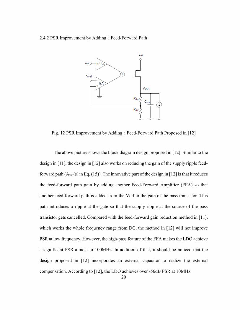
Fig. 12 PSR Improvement by Adding a Feed-Forward Path Proposed in [12] ................ 20
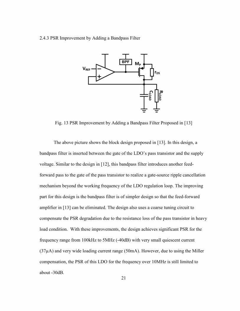
Fig. 13 PSR Improvement by Adding a Bandpass Filter Proposed in [13] ..................... 21
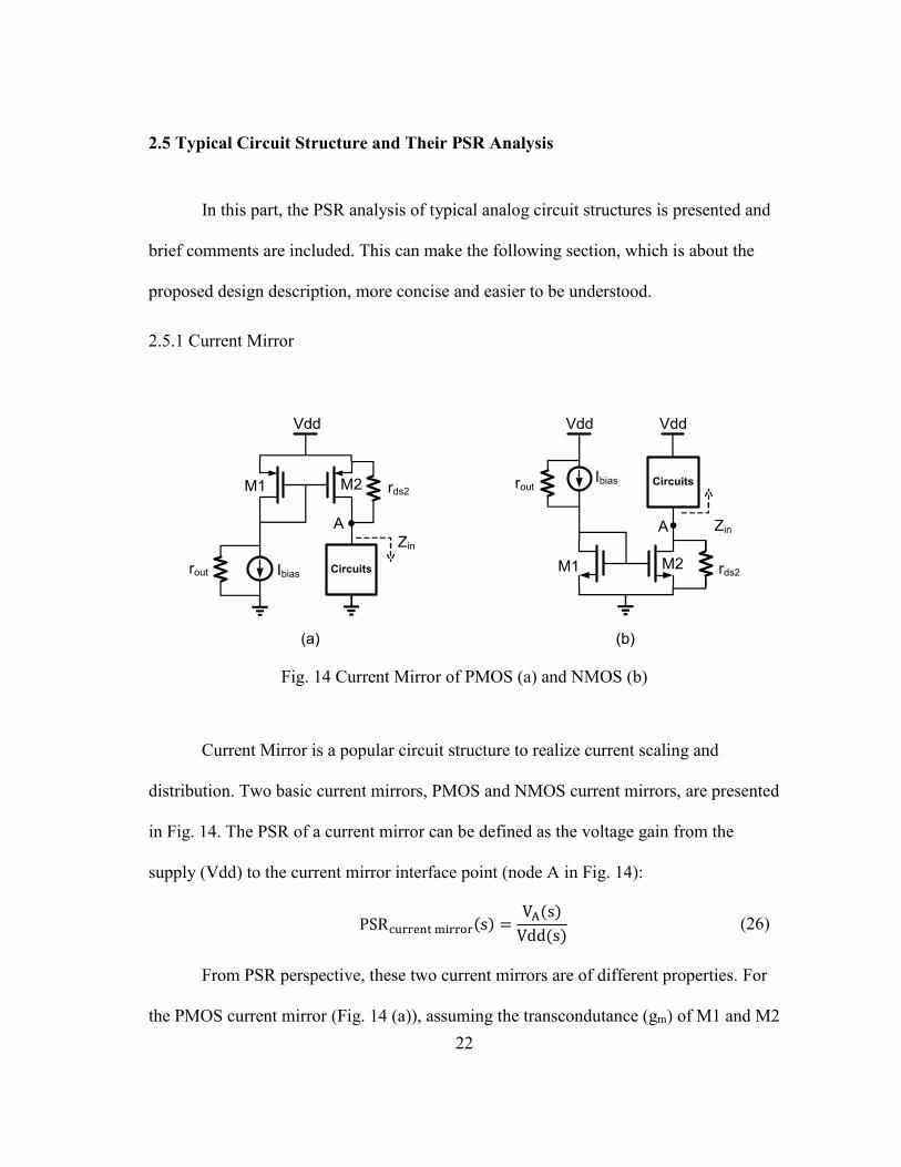
Fig. 14 Current Mirror of PMOS (a) and NMOS (b) ....................................................... 22
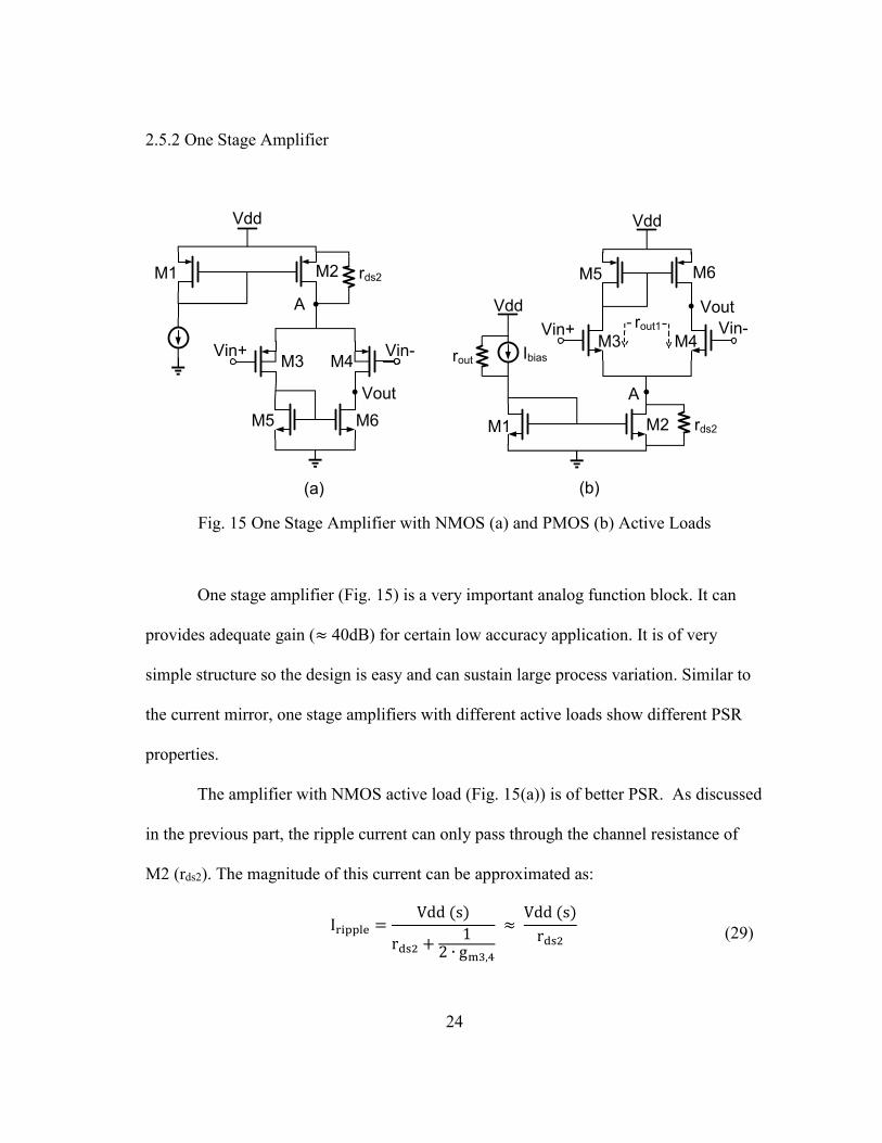
Fig. 15 One Stage Amplifier with NMOS (a) and PMOS (b) Active Loads ................... 24
Fig. 16 PMOS (a) and NMOS (b) Voltage Follower ....................................................... 26
Fig. 17 Small Signal Model of NMOS Voltage Follower ................................................ 27
Fig. 18 Basic LDO Structures with PMOS (a) and NMOS (b) Pass Transistor .............. 28
Fig. 19 System Design of the Proposed Main LDO Circuit ............................................. 32
Fig. 20 Proposed LDO Transistor Level Design with Triple-Well NMOS ..................... 33
ix
Fig. 21 Self-Cascode Current Sources in the Voltage Followers ..................................... 35
Fig. 22 Charge Pump Circuit Design ............................................................................... 36
Fig. 23 Proposed LDO Transistor Level Design with Zero-Vt NMOS ........................... 37
Fig. 24 Concept of Current Mode CM (a) and Simplified Design of Current Mode
CM Proposed in [17] (b) ...................................................................................... 38
Fig. 25 System Level Design of the Proposed CM .......................................................... 40
Fig. 26 Proposed CM and Its Connection to the Main LDO ............................................ 42
Fig. 27 Transistor Level Implementation of Amplifier A1 in CM ................................... 43
Fig. 28 Transistor Level Implementation of Amplifier A2 in CM ................................... 44
Fig. 29 Amplifier with Output Offset Cancellation in [9] ................................................ 44
Fig. 30 Paths in the LDO with Triple-Well Introducing Supply Ripples to Vout ............. 45
Fig. 31 Simulated PSR due to the Three Paths in Fig. 30 with Iout = 10mA .................... 47
Fig. 32 Simulated PSR due to the Three Paths in Fig. 30 with Iout = 1mA ...................... 47
Fig. 33 Simulated PSR due to the Three Paths in Fig. 30 with Iout = 0.1mA ................... 48
Fig. 34 Paths in the LDO with Zero-Vt Introducing Supply Ripples to Vout ................... 48
Fig. 35 Simulated PSR due to the Three Paths in Fig. 34 with Iout = 10mA .................... 49
Fig. 36 Simulated PSR due to the Three Paths in Fig. 34 with Iout = 1mA ...................... 49
Fig. 37 Simulated PSR due to the Three Paths in Fig. 34 with Iout = 0.1mA ................... 50
Fig. 38 Four Critical Paths in the CM Affecting PSR of the LDO .................................. 51
Fig. 39 Small Signal Model of the Critical Paths in Fig. 38 ............................................ 51
Fig. 40 Modified Connection Relation between the Main LDO and the CM .................. 53
Fig. 41 Conceptual Diagram of the CM Supply Modification Effect on PSR ................. 54
Fig. 42 Simulation of PSR with and without Main LDO Protection for CM at 1mA
Loading Current ................................................................................................... 55

x
Fig. 43 Simulation of PSR with and without Main LDO Protection for CM at 10mA
Loading Current ................................................................................................... 55
Fig. 44 Non-Idealities inside the CM ............................................................................... 56
Fig. 45 Simulation Results of the Output Admittance of the CM .................................... 58
Fig. 46 Output Impedance of the Proposed Main LDO ................................................... 59
Fig. 47 Regulation Loop of Proposed Main LDO ............................................................ 60
Fig. 48 Output Admittance of the CM and Real Capacitor .............................................. 62
Fig. 49 Loop Gain Simulation of the LDO with Triple-Well NMOS with Different
Capacitive Loads .................................................................................................. 63
Fig. 50 Loop Gain Simulation of the LDO with Zero-Vt NMOS with Different
Capacitive Loads .................................................................................................. 63
Fig. 51 CM Parasitic Loop ............................................................................................... 64
Fig. 52 Simulation of the CM Loop Frequency Response with Triple-Well LDO
with and without C1 ............................................................................................. 68
Fig. 53 Simulation of the CM Loop Frequency Response with Zero-Vt LDO with
and without C1 ..................................................................................................... 68
Fig. 54 Paths in the CM Loop Created by the LDO Protection ....................................... 69
Fig. 55 CM Loop Frequency Response with and without Extra Paths ............................ 69
Fig. 56 Supply Voltage Limit of the Main LDO with Triple-Well NMOS ..................... 71
Fig. 57 Supply Voltage Limit of the Main LDO with Zero-Vt NMOS ........................... 72
Fig. 58 Current Consumption and CM Output Equivalent Capacitance .......................... 74
Fig. 59 Layout Profile of the LDO with Triple-Well ....................................................... 80
Fig. 60 Layout Profile of the LDO with Zero-Vt ............................................................. 81
Fig. 61 Small Signal Equivalent Network of the CM ...................................................... 81
Fig. 62 Output Equivalent Admittance Comparison between the CM and the
Equivalent Network in Fig. 61 ............................................................................. 82

xi
Fig. 63 PSR Simulation of the LDO with Triple-Well..................................................... 83
Fig. 64 PSR Simulation of the LDO with Zero-Vt .......................................................... 83
Fig. 65 Loop Gain Frequency Response of the LDO with Triple-Well ........................... 84
Fig. 66 Loop Gain Frequency Response of the LDO with Zero-Vt ................................. 85
Fig. 67 CM Loop Frequency Response When Connected to LDO with Triple-Well ...... 87
Fig. 68 CM Loop Frequency Response When Connected to LDO with Zero-Vt ............ 88
Fig. 69 Load Transient of the LDO with Triple-Well ...................................................... 89
Fig. 70 Transient Response of the LDO with Triple-Well for a Current Step Up ........... 90
Fig. 71 Transient Response of the LDO with Triple-Well for a Current Step Down ...... 90
Fig. 72 Line Transient Response of the LDO with Triple Well for Iout = 10mA ............. 91
Fig. 73 Line Transient Response of the LDO with Triple Well for Iout = 1mA ............... 91
Fig. 74 Line Transient Response of the LDO with Triple Well for Iout =100µA ............. 92
Fig. 75 Load Transient of the LDO with Zero-Vt ............................................................ 92
Fig. 76 Transient Response of the LDO with Zero-Vt for a Current Step Up ................. 93
Fig. 77 Transient Response of the LDO with Zero-Vt for a Current Step Down ............ 93
Fig. 78 Line Transient Response of the LDO with Zero-Vt for Iout = 10mA ................... 94
Fig. 79 Line Transient Response of the LDO with Zero-Vt for Iout = 1mA ..................... 94
Fig. 80 Line Transient Response of the LDO with Zero-Vt for Iout = 100µA .................. 95
Fig. 81 Transient Simulation Results of the Charge Pump and LDO Output .................. 95
Fig. 82 Transient Simulation Result of the CM ............................................................... 96
Fig. 83 Simplified Schematic of the PCB Test Board ...................................................... 97
Fig. 84 PCB Test Board ................................................................................................... 99
Fig. 85 Load Regulation of the LDO with Triple-Well ................................................. 100
Fig. 86 Line Regulation of the LDO with Triple-Well .................................................. 101

xii
Fig. 87 Load Transient Test Results for 10µA to 10mA (a) and 10mA to 10µA (b) .... 102
Fig. 88 Line Transient Test of the LDO with Triple-Well for Iout = 10mA ................... 102
Fig. 89 Line Transient Test of the LDO with Triple-Well for Iout = 1mA ..................... 103
Fig. 90 Line Transient Test of the LDO with Triple-Well for Iout = 100µA .................. 103
Fig. 91 PSR Test Results of the LDO with Triple-Well ................................................ 104
Fig. 92 Time Domain Charge Pump Output and LDO’s Output ................................... 105
Fig. 93 FFT Analysis of the LDO Output Voltage ........................................................ 105
Fig. 94 Load Regulation Test Results of the LDO with Zero-Vt NMOS ...................... 106
Fig. 95 Line Regulation Test Results of the LDO with Zero-Vt NMOS ....................... 107
Fig. 96 Load Transient Test Results for 10µA to 10mA (a) and 10mA to 10µA (b) .... 108
Fig. 97 Line Transient Test of the LDO with Zero-Vt for Iout = 10mA ......................... 108
Fig. 98 Line Transient Test of the LDO with Zero-Vt for Iout = 1mA ........................... 109
Fig. 99 Line Transient Test of the LDO with Zero-Vt for Iout = 100µA ........................ 109
Fig. 100 PSR Test Result of the LDO with Zero-Vt ...................................................... 110

xiii
LIST OF TABLES
Page
Table 1 Design Parameters of the Simple LDOs ............................................................... 9
Table 2 System Design Parameters of the Main LDO ..................................................... 76
Table 3 System Design Parameters of the CM ................................................................ 77
Table 4 Transistor Level Design of the LDO with Triple-Well Pass Transistor ............. 78
Table 5 Transistor Level Design of the Charge Pump in the LDO with Triple-Well ...... 78
Table 6 Transistor Level Design of the LDO with Zero-Vt Pass Transistor ................... 79
Table 7 Transistor Level Design of the CM ..................................................................... 79
Table 8 UGF and PM of the Regulation Loop of the LDO with Triple-Well .................. 85
Table 9 UGF and PM of the Regulation Loop of the LDO with Zero-Vt ........................ 86
Table 10 UGF and PM of the CM Loop Connected to the LDO with Triple-Well ......... 87
Table 11 UGF and PM of the CM Loop Connected to the LDO with Zero-Vt ............... 88
Table 12 Summary of the Test Results of the Proposed LDOs ..................................... 111
Table 13 Comparison Table of the Proposed LDOs with the State of Arts Design ....... 113

1
1. INTRODUCTION
Power management systems designed for mobile electronics draw great research
interest due to the prevalence of smart phones and tablets. A typical power management
system of a mobile device is shown in Fig. 1.
Lithium
Battery
Switching Regulator
Boost
Converter
Buck
Converter
3V-5V
LED
Drivers
LDO
Analog
LDO
RF
Digital
Circuits
Analog
Circuits
RF
Circuits
10V-20V
1V-5V
1V-1.8V
1.8V-3V
Power Management System
Fig. 1 Power Management System of Mobile Electronics
The power system in Fig. 1 consists of two stages. The first stage is made of
switching regulators, which transform the fixed battery voltage into different DC voltage
levels to power different function blocks. For example, a boost converter can raise its
output voltage from lithium battery to power high voltage blocks, such as LED drivers
for display back-lights. A buck converter can step down the supply voltage for low
voltage blocks, such as RF, analog and digital circuits. The power efficiency of
switching regulators is very high (> 90%) due to its switching nature. Therefore, they are

2
preferred as the first stage to maintain good power efficiency of the system. However,
the switching behavior of switching regulators introduces voltage ripples to their output
and disturbs noise sensitive circuits such as analog and RF signal processing circuits. To
suppress the switching ripples, LDOs are added as the second stage of the power system.
Being of continuous time regulating nature, LDOs are able to provide much cleaner
supply voltages but of relatively lower power transform efficiency (< 85%).
As indispensable components of power management system of mobile devices,
LDOs play an importance role in defining the whole power system’s performance. The
key design criteria for LDOs includes fast transient response, small quiescent current
consumption and high power supply rejection (PSR) over wide frequency range. In this
thesis, an external-capacitor-free (capacitor-less) LDO compensated by a capacitance
multiplier (CM) with significant PSR over wide frequency range is presented.
1.1 Design Motivation
A capacitor-less LDO with high PSR at high frequency is highly desired in
mobile devices. Firstly, a capacitor-less LDO does not require a pin in the power
management integrated circuit (PMIC) package to connect to an external capacitor for
stabilization. With reduced pin number, the chip package area, PCB allocation area and
on-board routing complexity of the PMIC get reduced. This helps realizing more
compact devices. Secondly, to maintain long battery life, mobile devices frequently
switch between different working modes (i.e. sleep mode and active mode). This
requires PMICs to be of fast transient response. As the first stage of the power
3
management system, switching regulators can boost their transient response by
increasing their switching frequencies [1]. Therefore, following the switching regulator,
LDOs should be of the PSR bandwidth no less than the switching frequency of the
switching regulator so that the switching ripples will not affect the noise sensitive
circuits (i.e. ADCs and VCOs).
For the state of art, the switching regulators with working frequency over 10MHz
has appeared with significant transient speed improvement and compact design [2][3][4].
Also many ADCs [5][6] and VCOs [7][8] designs are using current between 2mA and
20mA. Therefore, a capacitor-less LDO with PSR over 10MHz and maximum supply
current 10mA is a practical and useful component of a power management system.
1.2 Thesis Organization
The following content of this thesis contains five sections: Section 2 gives a brief
introduction of fundamentals related to the LDO structure, design and PSR analysis;
Section 3 presents the proposed LDO design from system level to transistor level and the
stability analysis; Section 4 provides the simulation results of the proposed design to
concrete the working principles of the circuits. Also, the layout profile is presented in
this section; Section 5 provides the test results of the circuit fabricated in IBM 0.18µm
technology to verify the feasibility of the proposed designs; Section 6 concludes this
thesis and comments the proposed design. A comparison between the proposed design
and some other state-of-art LDO designs is also included in this section.
4
2. FUNDAMENTALS
2.1 LDO Introduction
An ideal voltage source is preferred for all kinds of circuits because it can supply
any amount of current without supply voltage variation. A LDO is used to approximate
an ideal voltage source in real life. Within its loading current range, the output voltage of
a LDO (Vout) should be of very little variation with respect to different loading currents.
VREF
Vin
R1
R2
EA
CL Iout
Vout
MPVFB
Fig. 2 A Typical LDO Design
A typical design of LDO contains three parts as shown in Fig. 2. The pass
transistor (MP) is the power device, through which the current comes to the load. The
drain current of the pass transistor can be modeled by the equation:
IMP =
1
2μCox
W
L(VGS − Vth)
2 (1)
By tuning the gate voltage of the pass transistor, the corresponding load current (Iout)
demand can be met while a relatively constant output voltage is maintained. The gate
5
voltage tuning mechanism is done by the feedback network and the error amplifier (EA).
The feedback network is usually made up of a resistive voltage divider, as R1 and R2
shown in Fig. 2. They feedback a fraction of output voltage (VFB) to the error amplifier:
VFB = Vout ∙
R2
R1 + R2 (2)
This feedback voltage is compared by the EA with a reference voltage (VREF). The
output voltage of the EA is produced according to the error voltage between the
reference voltage and the feedback voltage. This output voltage tunes the gate drive
voltage of the pass transistor to provide the demanded load current. For an ideal EA with
infinite gain, the output voltage of an LDO is:
Vout = Vref ∙ (1 +
R1
R2) (3)
For non-ideal EA with finite gain as AEA, an error voltage is created in the LDO output
voltage (Vout). The output voltage is then modified as shown in Eq. (4). It can be seen
that an error voltage about Vref ∙(1+
R1
R2)2
AEA is added to the LDO output.
Vout = VrefAEA
1 + AEA ∙R2
R1 + R2
≈ Vref ∙ (1 +R1
R2) − Vref ∙
(1 +R1R2)
2
AEA (4)
Though drawn as a PMOS in Fig. 2, a pass transistor in LDO can also be
implemented by a NMOS. The main differences between the LDO with NMOS pass
transistor and the one with PMOS lies in their output voltages and output impedance at
high frequency. This point influences the pass transistor selection in the proposed design
and is detailed discussed in Section 2.5.
6
2.2 LDO Characterization Parameters
For evaluating the performance of a LDO, parameters including drop-out
voltage, line and load regulation, power supply rejection and power efficiency are
frequently used. In this part, a brief description of these parameters is provided.
2.2.1 Drop-Out Voltage
Drop-Out Voltage is defined as the voltage difference between the LDO supply
voltage (Vin) and the LDO output voltage (Vout):
Vdrop−out = Vin − Vout (5)
The minimum Vdrop-out of a LDO is usually set by the saturation voltage (Vdsat) of
the pass transistor. If the drop-out voltage is less than Vdsat, the pass transistor goes into
triode region and cannot be described by Eq. (1). In this case, the LDO’s regulation
ability is quite degraded, which should be avoided.
For LDOs using PMOS as pass transistor, to avoid working in the triode region,
the minimum drop-out voltage should be larger than the Vdsat of the pass transistor as
shown in Eq. (6).
Vdrop−out PMOS ≥ Vdsat−MP (6)
For LDOs using NMOS pass transistor, the minimum drop-out voltage depends
on the maximum error amplifier output voltage (Vout-EA max) and the maximum gate-
source voltage of the pass transistor (Vgs-MP max).Mathematically, this relation is
described in Eq. (7):
Vdrop−out NMOS ≥ Vin − (Vout−EA max − Vgs−MP max) (7)

7
2.2.2 Line Regulation
Line Regulation (LNR) is defined as the static ratio between the Vout variation
and Vin variation when Vin changes its value:
LNR =
∆Vout∆Vin
(8)
According to Mason’s rule, the LNR can be expressed as:
LNR =
Avin1 + ALoop
≈ AvinALoop
(9)
In the above equation, Avin is the static gain value from Vin to Vout when the regulation
loop is disabled. ALoop is the static gain of the regulation loop.
2.2.3 Load Regulation
Load Regulation (LDR) is defined as the static ratio between the Vout variation
and load current, Iout variation:
LDR =
∆Vout∆Iout
(10)
Without specification, the load regulation can also be referred as the Vout changes when
the Iout varies from the minimum operating value to the maximum operating value.
2.2.4 LDO Output Impedance
Another parameter which can be used to describe the LDO’s load regulation
ability is the output impedance of the LDO. From Eq. (10) it can be seen that the load
regulation of a LDO is of the unit as impedance. To have small output impedance is
8
equivalent to have small load regulation because a port with small output impedance
varies its output voltage little when output current changes.
The LDO output impedance can also be used to estimate the LDO’s dynamic
regulation ability because it reflects the frequency response of the LDO at its output. The
output impedance can be calculated according to its open loop output impedance and
regulation loop gain:
ZOUT−LDO =
Vout(s)
Iout(s)=
ZOUT−OL1 + ALoop(s)
(11)
According to Eq. (11), a LDO with high regulation loop gain across a wide frequency
range can maintain a low output impedance of the LDO in wide frequency range. This
means the LDO can regulate fast transient current with smaller output overshoot voltage.
Another interesting point about the LDO output impedance is to compare the
output impedance between the LDOs with NMOS and PMOS pass transistors. For
illustration convenience, two simple LDOs with NMOS and PMOS pass transistors are
drawn in Fig.3, in which capacitor Cc is the compensation capacitor.
VREFM1 M1
M2 M2MPP
Iout
CcM1 M1
M2 M2
MPN
Iout
Cc
ItailItail
(a) (b)
VREF
Fig. 3 Simple LDOs with PMOS (a) and NMOS (b) Pass Transistor

9
Denoting the transconductance of the PMOS and NMOS pass transistors as gmP
and gmN, their channel resistance as gdsP and gdsN and the error amplifier gain as AEA (s).
The output impedance of the LDO with PMOS pass transistor (ZOUT-P) and the LDO
with NMOS pass transistor (ZOUT-N) can be expressed as:
ZOUT−P =
1/gdsP
1 + AEA(s) ∙gmPgdsP
≈1
AEA(s) ∙ gmP (12)
ZOUT−N =
1/gmN1 + AEA(s)
≈1
AEA(s) ∙ gmN (13)
It can be seen that, at low frequency, the two kinds of LDOs are of almost same output
impedance. However, at the high frequency, when the gain of the regulation loop can be
ignored, the LDO with NMOS pass transistor is of much higher output impedance than
that of LDO with PMOS for its much lower open-loop output impedance. This helps the
LDO with NMOS pass transistor to get a faster load transient response with smaller
overshoot voltage.
To illustrate this point, the circuit in Fig.3 is implemented with the parameters
shown in Table 1. The two LDOs are of the same error amplifier and same pass
transistor size. Their output impedance is measured in simulation and shown in Fig.4.
W/L Value
M1 80µm / 2.4µm Cc 100pF
M2 120µm / 2.4µm Iout 50mA
MPN 2000µm / 0.18µm VREF 0.8V
MPP 2000µm / 0.18µm Itail 40µA
Table 1 Design Parameters of the Simple LDOs
10
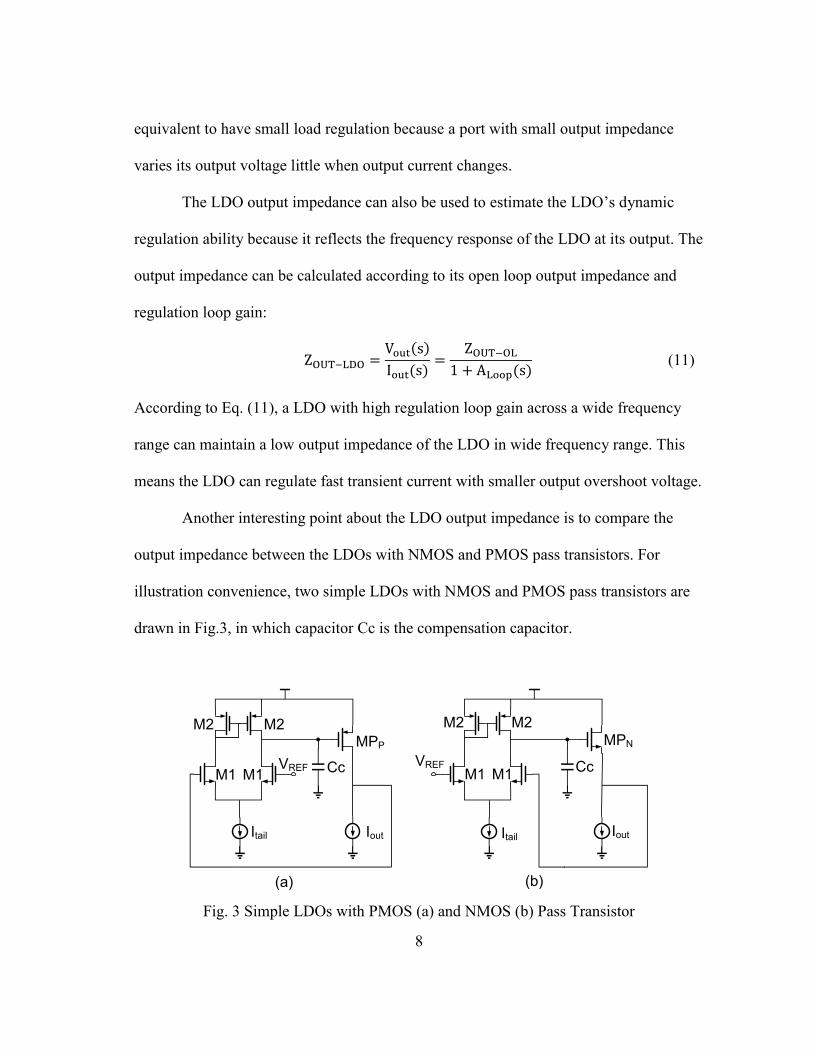
Fig. 4 Output Impedance Comparison for the LDO with NMOS and PMOS Pass
Transistor
It can be seen from Fig. 4 that, at low frequency, the output impedance of a LDO
with NMOS pass transistor is of the same order with the one with PMOS. However, at
high frequency, when the regulation loop stop working, the output impedance of a LDO
with NMOS is much smaller than the LDO with PMOS pass transistor.
The lower output impedance at high frequency of the LDO with NMOS pass
transistor provides itself better load transient response. In the simulation, a current pulse
with peak value 1mA and 50mA, rise and fall time 100ns is applied to the two simple
LDO designed according to Table 1. The transient simulation results are shown in Fig. 5.
For the LDO with NMOS, the overshoot voltage is about 50mV while for the PMOS
one, the over shoot voltage is over 1.8V. This proves the point that the LDO with a
NMOS pass transistor is of lower output impedance over wide frequency range. In
Section 3.4, it is discussed that this merit helps the stability design of the CM.

11
Fig. 5 Load Transient Response Comparison for the LDO with NMOS and PMOS Pass
Transistor
2.2.5 Power Supply Rejection
Power Supply Rejection is defined as the gain value from Vin to Vout (Fig. 2) with
respect to different frequency changes:
PSR(s) =
VoutVin
(s) (14)
Analyzing with Mason’s Rule, PSR can be expressed as:
PSR (s) =
Avin(s)
1 + ALoop(s) (15)
In the above equation, Avin(s) is the gain frequency response from Vin to Vout when the
regulation loop is disabled. ALoop(s) is the regulation loop gain frequency response. It
12
can be seen that the PSR is a generalization of line regulation in frequency perspective.
It describes a LDO’s dynamic regulation ability towards dynamic signals from the power
supply. From Eq. (15) it can be concluded that, to improve the PSR, either should Avin be
reduced or Avin be increased.
The power supply rejection ratio (PSRR) is another term describing a circuit’s
immunity to the supply noise. The PSRR is always applied to amplifiers and defined as
the gain of the amplifier divided by its gain from the supply to the output [9]. Comparing
this definition of PSR, it can be seen that a circuit’s PSR is of the same value with its
PSRR when it is used in a unity gain feedback loop. Therefore, though PSRR is a term
defined for open loop case, it defines a circuit’s maximum supply noise rejection ability
when used in a close loop system.
2.2.6 Power Efficiency
Power efficiency (η) is defined as the ratio between the power supplied to the
LDO’s load and the power the LDO receives from the power source:
η =
Vout ∙ IoutVin ∙ (Iout + IQ)
(16)
In the above equation, IQ is the current consumption of the LDO when Iout = 0A. IQ is
often referred as the quiescent current. Usually the LDO’s quiescent current is much
smaller than its maximum load current. Therefore, LDO’s efficiency for full load current
case can be approximated as the ratio between the output voltage and input voltage:
η|Iout=Imax ≈
VoutVin
(17)

13
2.3 LDO Compensation Strategies and Effects on PSR
In a LDO, the pass transistor, feedback network and error amplifier implement a
negative feedback. This feedback loop is referred as the regulation loop (Fig. 6).
VREF
Vin
CL
Iout
Vout
MP
Cgd-MP
Cgs-MP
AB
Regulation
Loop
Fig. 6 LDO Regulation Loop.
The parasitic poles in the regulation loop adds extra phase to the control signal
passing inside the loop. If two poles are close in frequency so that the total phase added
is over 180o before the loop gain drops below 0dB, the negative feedback regulation loop
becomes a positive one, which causes instability. In practical case, the poles at the gate
of the pass transistor (pA at node A in Fig.6) and at the output of LDO (pB at node B in
Fig.6), are very close in frequency:
ωpA =
1
rout1Cgs−MP + rout1(1 + gm−MProut2)Cgd−MP (18)
ωpB =
1
rout2CL (19)

14
In the above equations, rout1 and rout2 are output impedance at node A and B. gm-MP is the
transconductance of the pass transistor.
In LDO design, compensation is referred to the design to separate poles which
are close in frequency domain. Without any compensation, a LDO can always be
unstable due to the two poles described in Eq. (18) and (19) (Fig. 7(a)). Therefore,
different compensation strategies are used to separate these two poles in frequency
domain for LDO stabilization (Fig. 7(b)).
pA ( pB )
pB ( pA )
UGF
Gain
(dB)
log(f)pB ( pA )
UGF
Gain
(dB)
Phase
(deg)
0 0
0
-180
Phase
(deg)0
-90
(a) (b)
pA ( pB )
log(f)
-180
Fig. 7 Uncompensated (a) and Compensated (b) Frequency Response of LDO
Regulation Loop
Two types of LDO compensation strategies, namely the internal compensation
and the external compensation, can be used to separate the two poles. They have
different effects on the PSR of a LDO. This is demonstrated in the following paragraphs.

15
2.3.1 Internal Compensation
VREF
Vin
CL
IL
Vout
MP
Cgd-MP
Cgs-MP
AB
EASupply Ripple Feed-
Forward Path
Cc
Fig. 8 Typical Internally Compensated LDO
A typical internally compensated LDO is shown in Fig. 8. In this compensation,
a capacitor Cc is added between node A and B. Taking advantage of the gain of the pass
transistor (AMP= gm-MP∙rout2), the equivalent capacitance at node A is about AMP∙Cc [9].
This effect is called Miller Effect, so the internal compensation is also referred as Miller
Compensation. At high frequency, this large capacitance can be taken as a short circuit.
Therefore the pole frequency at node B gets raised. The pole frequencies at node A and
B after internal compensation become:
ωpA =
1
rout1Cgs−MP + rout1(1 + AMP)(Cc + Cgd−MP) (20)
ωpB =gm−MP
CL + Cgs−MP (21)
It can be seen that for internal compensation, the two poles get separated by decreasing
the frequency of pA and increasing the frequency of pB. This compensation method is in

16
favored for capacitor-less LDO design because the required compensation capacitor
value (Cc) can be small due to the Miller Effect.
The disadvantage of the internal compensation is that it limits the PSR bandwidth
to the first dominant pole frequency, which is ωpA, of the LDO regulation loop [10].
This is due to regulation loop gain loss for the dominant pole. Therefore, the PSR
bandwidth of an internally compensated LDO is very limited and is usually about 1 kHz.
2.3.2 External Compensation
VREF
CLIout
Vout
MP
Cgd-MP
Cgs-MP
A
B
EA
Vin
Off-Chip Capacitor
Supply Ripple
Feed-Forward Path
Fig. 9 Typical Externally Compensated LDO
Instead of adding Cc between nodes A and B, external compensation is realized
by adding capacitance at LDO’s output node (Fig. 9). With a large load capacitance CL,
the pole frequencies of pA and pB become:
ωpA =
1
rout1(Cgs−MP + Cgd−MP) (22)
ωpB =
1
rout2CL (23)

17
Without the help from the Miller Effect and due to the relatively smaller impedance at
the drain node of the pass transistor, the capacitance added at the LDO output node for
external compensation is much larger than that used for internal compensation. The
capacitor value used in external compensation is usually in the nF or µF range, which is
too large to be integrated on-chip. Therefore, external compensation is usually realized
by using an off-chip capacitor, which requires a specific pin on chip package to be
connected to the on-chip circuit.
The advantage of external compensation is that the PSR bandwidth gets extended
to the second pole frequency of the regulation loop [10]. Intuitively, this can be understood
as, though the regulation loop starts to lose the gain at its first pole frequency, the gain
from Vin to Vout also gets suppressed due to CL shunts more noise current to the ground
after the first pole frequency. These two effects neutralize each other so that the PSR will
not be degraded at the regulation loop’s first pole frequency. Mathematically it can be
understood by observing the PSR transfer function:
PSR(s) =Avin(s)
1 + ALoop(𝑠) ≈
Avin(s)
ALoop(𝑠)=
Avin ∙1
1 + srout2CL
ALoop ∙1
(1 +sωpA
) (1 +sωpB
)
(24)
Since ωpB = 1/rout2CL, the PSR transfer function can be reduced as:
PSR(s) =
Avin
ALoop ∙1
(1 +sωpA
)
(25)
It can be seen that the PSR start to degrade at the second pole frequency (ωpA) when the
LDO is externally compensated.
18
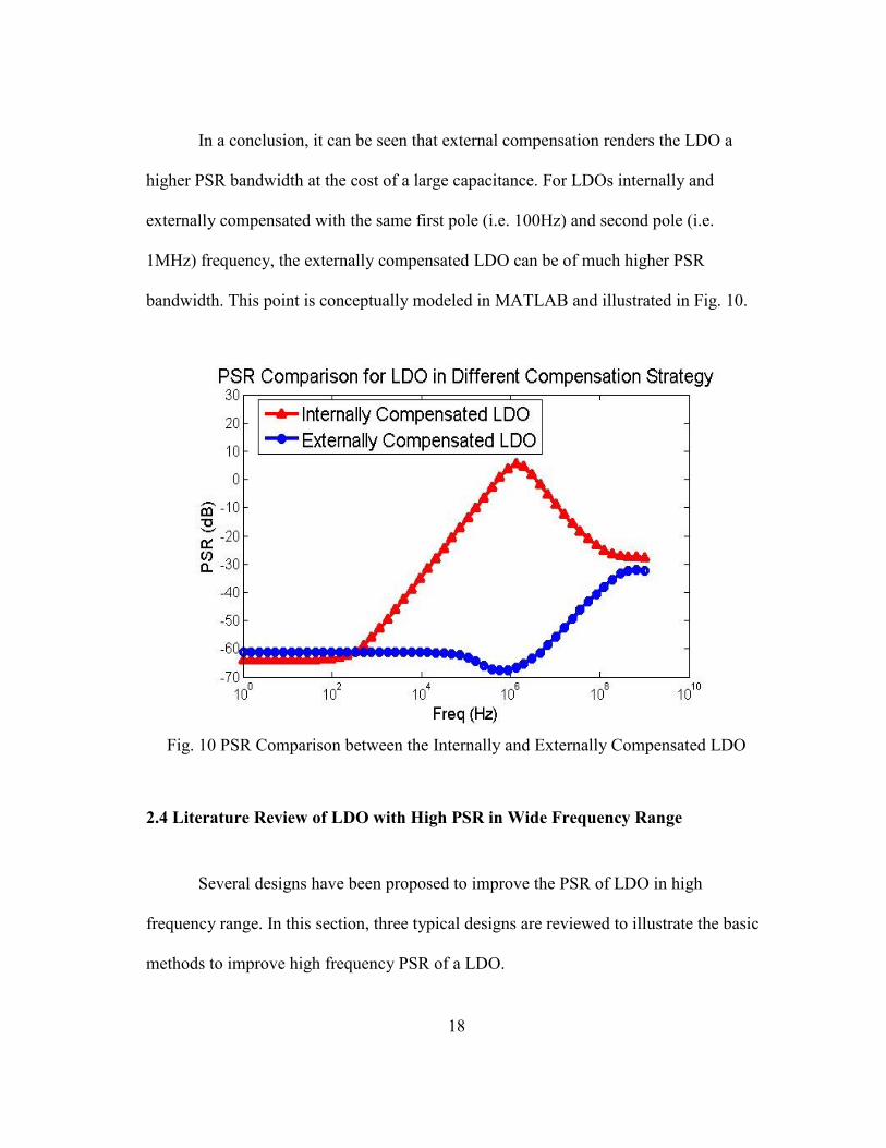
In a conclusion, it can be seen that external compensation renders the LDO a
higher PSR bandwidth at the cost of a large capacitance. For LDOs internally and
externally compensated with the same first pole (i.e. 100Hz) and second pole (i.e.
1MHz) frequency, the externally compensated LDO can be of much higher PSR
bandwidth. This point is conceptually modeled in MATLAB and illustrated in Fig. 10.
Fig. 10 PSR Comparison between the Internally and Externally Compensated LDO
2.4 Literature Review of LDO with High PSR in Wide Frequency Range
Several designs have been proposed to improve the PSR of LDO in high
frequency range. In this section, three typical designs are reviewed to illustrate the basic
methods to improve high frequency PSR of a LDO.

19
2.4.1 PSR Improvement by Adding Isolation Transistor
Charge
Pump
EA
MP
MNCR1
C1
RBIAS
Vout
VREF
Vin (> 1.8V)
CL
Vin (> 1.8V)(2.7V)
Fig. 11 PSR Improvement by Adding Isolation Transistor Proposed in [11]
The PSR of a LDO can be improved by using an NMOS (MNC in Fig. 11)
cascode stage to isolate the LDO pass transistor from Vin (Vdd) as proposed in [11]. This
reduces the gain from Vin (Vdd) to the LDO output (Avin(s) in Eq. (15)). The drawback
of adding a cascode isolation is that the drop-out voltage becomes higher (0.6V). Also,
the necessity of using a charge pump to driving the cascode device makes the design
more complex. As for the PSR at high frequency, due to using Miller Compensation in
the core LDO, the PSR over 10MHz is still limited. According to [11], the LDO
achieved -27dB PSR over 10MHz.
20
2.4.2 PSR Improvement by Adding a Feed-Forward Path
Fig. 12 PSR Improvement by Adding a Feed-Forward Path Proposed in [12]
The above picture shows the block diagram design proposed in [12]. Similar to the
design in [11], the design in [12] also works on reducing the gain of the supply ripple feed-
forward path (Avin(s) in Eq. (15)). The innovative part of the design in [12] is that it reduces
the feed-forward path gain by adding another Feed-Forward Amplifier (FFA) so that
another feed-forward path is added from the Vdd to the gate of the pass transistor. This
path introduces a ripple at the gate so that the supply ripple at the source of the pass
transistor gets cancelled. Compared with the feed-forward gain reduction method in [11],
which works the whole frequency range from DC, the method in [12] will not improve
PSR at low frequency. However, the high-pass feature of the FFA makes the LDO achieve
a significant PSR almost to 100MHz. In addition of that, it should be noticed that the
design proposed in [12] incorporates an external capacitor to realize the external
compensation. According to [12], the LDO achieves over -56dB PSR at 10MHz.
21
2.4.3 PSR Improvement by Adding a Bandpass Filter
Fig. 13 PSR Improvement by Adding a Bandpass Filter Proposed in [13]
The above picture shows the block design proposed in [13]. In this design, a
bandpass filter is inserted between the gate of the LDO’s pass transistor and the supply
voltage. Similar to the design in [12], this bandpass filter introduces another feed-
forward pass to the gate of the pass transistor to realize a gate-source ripple cancellation
mechanism beyond the working frequency of the LDO regulation loop. The improving
part for this design is the bandpass filter is of simpler design so that the feed-forward
amplifier in [13] can be eliminated. The design also uses a coarse tuning circuit to
compensate the PSR degradation due to the resistance loss of the pass transistor in heavy
load condition. With these improvements, the design achieves significant PSR for the
frequency range from 100kHz to 5MHz (-40dB) with very small quiescent current
(37µA) and very wide loading current range (50mA). However, due to using the Miller
compensation, the PSR of this LDO for the frequency over 10MHz is still limited to
about -30dB.
22
2.5 Typical Circuit Structure and Their PSR Analysis
In this part, the PSR analysis of typical analog circuit structures is presented and
brief comments are included. This can make the following section, which is about the
proposed design description, more concise and easier to be understood.
2.5.1 Current Mirror
Circuits
Vdd
M1 M2 rds2
Ibiasrout
Zin
Circuits
Vdd Vdd
Zin
M1 M2 rds2
(a) (b)
routIbias
A A
Fig. 14 Current Mirror of PMOS (a) and NMOS (b)
Current Mirror is a popular circuit structure to realize current scaling and
distribution. Two basic current mirrors, PMOS and NMOS current mirrors, are presented
in Fig. 14. The PSR of a current mirror can be defined as the voltage gain from the
supply (Vdd) to the current mirror interface point (node A in Fig. 14):
PSRcurrent mirror(s) =
VA(s)
Vdd(s) (26)
From PSR perspective, these two current mirrors are of different properties. For
the PMOS current mirror (Fig. 14 (a)), assuming the transcondutance (gm) of M1 and M2
23
is much larger than their channel conductance (gds) and the bandwidth of the current
mirror and the output resistance of the current reference (rout) is very large, the voltage
ripple at the gate of the current mirror is of the same amplitude as the supply ripple at
Vdd. Therefore, the only one path through which the supply ripple comes to the circuit
supplied is the channel resistance of M2. Thereby, it can be concluded that the PSR of a
PMOS current mirror is:
PSR(s) =
Zin(s)
Zin(s) + rds2 (27)
It can be seen that, designing M1 and M2 with longer transistor can improve the PSR of
the PMOS current mirror. This is due to that longer transistor is of larger channel
resistance (rds)[9] so that the PSR(s) in Eq. (27) can be reduced.
For the NMOS current mirror (Fig. 14(b)), ideally its PSR is negative infinity
because an ideal current source with infinite output impedance can shield M1 free from
the supply ripple. With finite output impedance of a current source (rout), a small amount
of supply ripples can leak to the gate of M1 and M2. Amplified by the transconductance
of M2, supply ripples appear at the interface between the current mirror and the supplied
circuits. The PSR of this mechanism can be approximated as:
PSR(s) =
1
1 + gm1rout∙ gm2(rd2||Zin) ≈
gm2(rd2||Zin)
gm1rout (28)
From Eq. (28), it can be concluded that increasing the output resistance of the current
source (Ibias) is an approach to improve the PSR of a NMOS current mirror. This can be
realized by using cascode, telescopic or more complex current mirror structures to
implement the current source.
24
2.5.2 One Stage Amplifier
Vdd
M1 M2 rds2
A
M3 M4
M5 M6
Vin+ Vin-
Vout
Vdd
Vdd
M1 M2 rds2
(b)
rout Ibias
A
M3 M4
M5 M6
Vin+ Vin-
(a)
Voutrout1
Fig. 15 One Stage Amplifier with NMOS (a) and PMOS (b) Active Loads
One stage amplifier (Fig. 15) is a very important analog function block. It can
provides adequate gain (≈ 40dB) for certain low accuracy application. It is of very
simple structure so the design is easy and can sustain large process variation. Similar to
the current mirror, one stage amplifiers with different active loads show different PSR
properties.
The amplifier with NMOS active load (Fig. 15(a)) is of better PSR. As discussed
in the previous part, the ripple current can only pass through the channel resistance of
M2 (rds2). The magnitude of this current can be approximated as:
Iripple =
Vdd (s)
rds2 +1
2 ∙ gm3,4
≈ Vdd (s)
rds2
(29)

25
This current is divided equally between the branches through M3 and M4. For this
common mode current, the input impedance of the current mirror of M5 and M6 is
1/gm5,6. Therefore, the PSR of the amplifier with PMOS input pair is:
PSR (s) ≈
Vdd (s)rds2
∙ gm5,6
Vdd (s)=
1
gm5,6 rds2
(30)
It can be seen that by using longer channel device for the tail current mirror (M2) can
improve the PSR of the amplifier.
The amplifier with PMOS active load (Fig. 15(b)) is of a PSR approximately
equal to 0dB. Though there is little supply ripple transferred by the current mirror of M1
and M2, the dominant supply ripple path is the current mirror composed of M5 and M6.
For common mode signal, the impedance of the current mirror of M5 and M6 is very
small (1/gm5,6), but M3, M4 and M5 make up of a cascode device in common mode
perspective. The common mode impedance of this structure (rout1 in Fig. 15(b)) is much
higher than that of the PMOS active load. Therefore, from the perspective of a voltage
divider, the supply ripple comes to the amplifier output node with little attenuation:
PSR (s) = rout1
1gm5,6
+ rout1
≈ 1 (31)
It can be concluded that the amplifier with PMOS active load is of 0dB PSR
because the PMOS current mirror creates a low common mode impedance between the
Vdd and the output node. This amplifier is also referred as Type A amplifier [14]. The
amplifier with NMOS active load is of better PSR due to the low common mode
impedance to the ground. This amplifier is also referred as Type B amplifier [14].
26
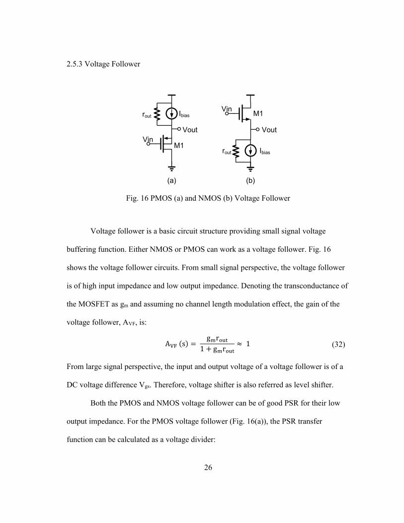
2.5.3 Voltage Follower
Vin
rout Ibias
Vout
Vin
rout
Vout
(b)
Ibias
(a)
M1
M1
Fig. 16 PMOS (a) and NMOS (b) Voltage Follower
Voltage follower is a basic circuit structure providing small signal voltage
buffering function. Either NMOS or PMOS can work as a voltage follower. Fig. 16
shows the voltage follower circuits. From small signal perspective, the voltage follower
is of high input impedance and low output impedance. Denoting the transconductance of
the MOSFET as gm and assuming no channel length modulation effect, the gain of the
voltage follower, AVF, is:
AVF (s) = gmrout
1 + gmrout≈ 1 (32)
From large signal perspective, the input and output voltage of a voltage follower is of a
DC voltage difference Vgs. Therefore, voltage shifter is also referred as level shifter.
Both the PMOS and NMOS voltage follower can be of good PSR for their low
output impedance. For the PMOS voltage follower (Fig. 16(a)), the PSR transfer
function can be calculated as a voltage divider:

27
PSR (s) =
1/gmrout + 1/gm
=1
1 + gmrout (33)
It can be seen that current bias with higher output impedance can help PMOS voltage
follower achieve good PSR.
The PSR of a NMOS voltage follower (Fig. 16(b)) can be analyzed from its small
signal model shown in Fig. 17. The channel resistance and transcondutance of M1 is
denoted as rds1 and gm1 in Fig. 17.
rout
Vdd
Vout
-gm1•Vout rds1
Fig. 17 Small Signal Model of NMOS Voltage Follower
Applying KCL law at node Vout, an equation can be got:
Vout ∙ (gm1 +
1
rout) =
Vdd − Vxrds1
(34)
Solving Eq. (34), we can find out the PSR of the NMOS voltage follower:
PSR(s) =
Vout
Vdd=
routrds1(1 + gm ∙ rout) + rout
(35)
It can be seen that the NMOS voltage follower can achieve a good PSR by increasing the
NMOS’s channel resistance.
28
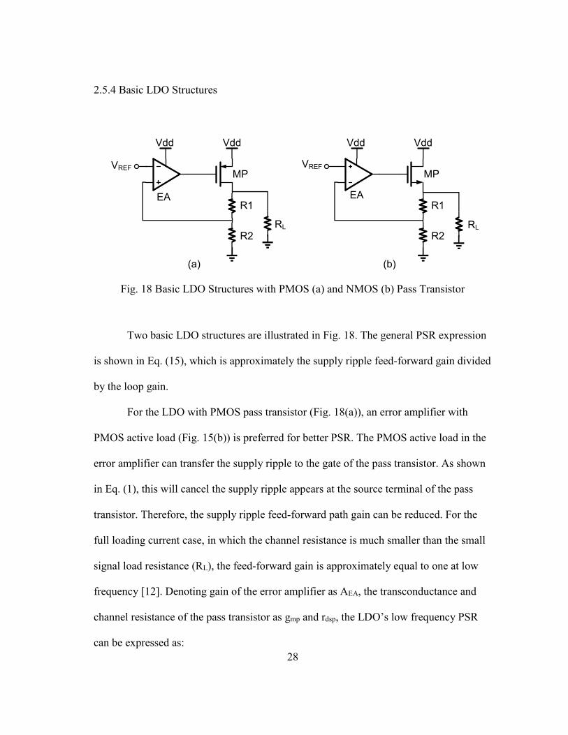
2.5.4 Basic LDO Structures
R1
R2
VddVdd
MP
EA EAR1
R2
VREF
VddVdd
MP
(a) (b)
RL
VREF
RL
Fig. 18 Basic LDO Structures with PMOS (a) and NMOS (b) Pass Transistor
Two basic LDO structures are illustrated in Fig. 18. The general PSR expression
is shown in Eq. (15), which is approximately the supply ripple feed-forward gain divided
by the loop gain.
For the LDO with PMOS pass transistor (Fig. 18(a)), an error amplifier with
PMOS active load (Fig. 15(b)) is preferred for better PSR. The PMOS active load in the
error amplifier can transfer the supply ripple to the gate of the pass transistor. As shown
in Eq. (1), this will cancel the supply ripple appears at the source terminal of the pass
transistor. Therefore, the supply ripple feed-forward path gain can be reduced. For the
full loading current case, in which the channel resistance is much smaller than the small
signal load resistance (RL), the feed-forward gain is approximately equal to one at low
frequency [12]. Denoting gain of the error amplifier as AEA, the transconductance and
channel resistance of the pass transistor as gmp and rdsp, the LDO’s low frequency PSR
can be expressed as:

29
PSR ≈
1
1 + AEA ∙ gmp ∙ rdsp≈
1
AEA ∙ gmp ∙ rdsp (36)
For the LDO with NMOS pass transistor (Fig. 18(b)), an error amplifier with
NMOS active load (Fig. 15(a)) is more suitable for achieving good PSR. As discussed in
Section 2.5.2, through careful design, the output voltage of the error amplifier can be
assumed as supply ripple free. Therefore, the main supply ripple feed-forward path lies
in the pass transistor. As for the pass transistor, the feed-forward path analysis is same as
a NMOS voltage follower in Section 2.5.3. Assuming the small signal loading resistance
of the LDO (RL) is much larger than the channel resistance of the pass transistor, the
supply ripple feed-forward gain of the LDO with NMOS pass transistor, Avin, can be
approximated as:
Avin =
rout
rdsp(1 + gmp ∙ rout) + rout≈
1
gmp ∙ rdsp (37)
Thereby, the low frequency PSR of the LDO with NMOS pass transistor can be
expressed as:
Avin =
1gmp ∙ rdsp
1 + AEA≈
1
AEA ∙ gmp ∙ rdsp
(38)
Comparing Eq. (36) and Eq. (38), it can be seen that using either NMOS or
PMOS as the pass transistor in a LDO does not necessarily create significant PSR
difference if appropriate error amplifier is used.
30
3. PROPOSED LDO DESIGN
From the previous discussion, it can be seen that there is a strong trade-off in the
LDO design between achieving good PSR in wide frequency range and realizing a LDO
without external capacitor. To achieve a wide PSR bandwidth, external compensation
should be used in the LDO. However, due to the large size of the pass transistor, the
impedance at the output node of the LDO is much larger than any other internal nodes in
the LDO regulation loop. Moreover, since the capacitor used for external compensation
is directly connected to the ground, there is no Miller Effect coming in the scenario for
enhance the capacitive effect at the output node. These two effects make the capacitor
entailed for external compensation is of nF or even µF order. To realize a capacitor in
this value on chip, extremely large area becomes an unaffordable cost due to the limited
capacitor density on-chip (~2fF/µm2).
To realize an externally compensated LDO while maintain a fully on-chip
design, a large equivalent capacitance should be created using the limited on-chip
capacitance. In this thesis, a CM circuit is proposed to amplify a limited on-chip
capacitor to a capacitance comparable to an external capacitor. With this large
capacitance, a LDO can be externally compensated and achieves a good PSR in wide
frequency range. However, the large amplification factor of the CM makes it easy to go
into unstable state. Therefore, the LDO connected to it should be carefully designed to
stabilize the CM.
31
In the transistor level design, two main LDO circuits are designed to work with
the same CM. The main difference between the two LDO circuits lies in the pass
transistor. One LDO design incorporates a triple-well NMOS pass transistor. The triple-
well NMOS pass transistor is of normal threshold voltage (~ 500mV). Therefore, a
charge pump is included in the LDO to provide a gate drive voltage higher than the
supply voltage. The other LDO uses Zero-Vt NMOS as the pass transistor. The Zero-Vt
NMOS is of negative threshold voltage (~ −100mV) so that the charge pump can be
eliminated. However, the Zero-Vt NMOS is of much larger size. This makes the LDO
consume more power and of reduced PSR bandwidth.
In the following context, the proposed LDO system, including the main LDO and
the CM circuit will be described from system level to transistor level. The basic design
idea is qualitatively described in Section 3.1 and 3.2. The PSR design issue is discussed
in Section 3.3. The stability design issue is elaborated in Section 3.4. The quantitative
design parameters developed based on above discussion is presented in Section 3.5.
3.1 Main LDO Design
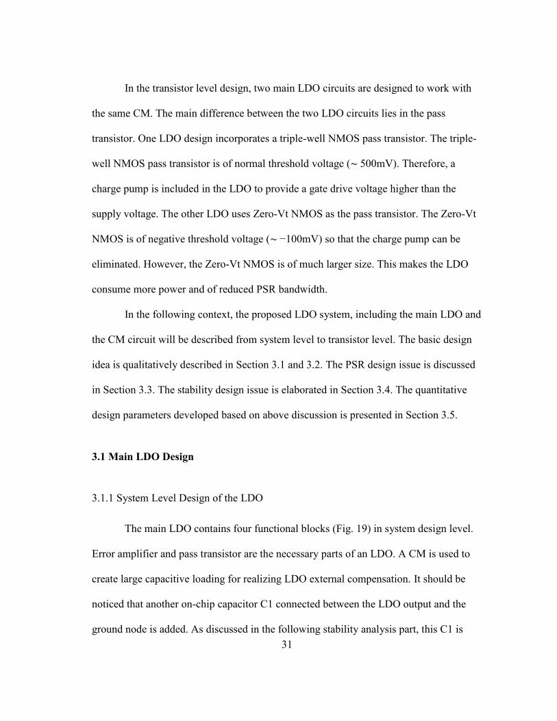
3.1.1 System Level Design of the LDO
The main LDO contains four functional blocks (Fig. 19) in system design level.
Error amplifier and pass transistor are the necessary parts of an LDO. A CM is used to
create large capacitive loading for realizing LDO external compensation. It should be
noticed that another on-chip capacitor C1 connected between the LDO output and the
ground node is added. As discussed in the following stability analysis part, this C1 is
32
necessary for stabilize both the main LDO and CM. To achieve a wide PSR bandwidth,
the first non-dominant pole of the regulation loop should be of high frequency according
to Eq. (25). Therefore, a voltage buffer is inserted between the pass transistor and the
error amplifier. With the small output impedance of the voltage buffer, the pole
frequency at the gate of the pass transistor can be increased. Though with increased pole
frequency, the first non-dominant pole of the regulation loop is still at the gate of the
pass transistor due to the large parasitic capacitance at the gate of the pass transistor.
CM
Error
Amplifier
Voltage
Buffer
Pass
Transistor
Capacitance
Multiplier
R1
R2
C1
VREF
Fig. 19 System Design of the Proposed Main LDO Circuit
It should be pointed out that, from system design perspective, the pass transistor
can be implemented by either a PMOS or a NMOS. However, in the proposed design, a
NMOS is chosen as the pass transistor. As shown in Section 2.2.4, a LDO with NMOS
pass transistor is of a lower output impedance in a wider frequency range. This helps the
stability design of the CM. The detailed information of the CM stability design is
presented in Section 3.4.

33
3.1.2 Transistor Level Design of the LDO with Triple-Well NMOS Pass Transistor
Error
Amplifier
Voltage
Buffer
Pass
Transistor
VREF
M1 M1
M2 M2
M4 M4
2x CP
CMM3
Ibias2
R1
R2C1
M5 M5
M6
MP
Triple-Well
Capacitance
Multiplier
Ibias3
M7Ibias1
Fig. 20 Proposed LDO Transistor Level Design with Triple-Well NMOS
The above picture shows the transistor level design of the main LDO part. For
the error amplifier, a folded cascode one stage amplifier (M1-5) is used. As discussed in
Section 2.4, an amplifier with NMOS active load is suitable for working with a NMOS
pass transistor because it can strongly attenuate the supply ripple at its output node. The
reason for using a NMOS input pair is because reference voltage (1.0V) is closer to the
positive supply rail (1.8V). If a PMOS input pair with threshold voltage about 500mV is
used, the voltage room for the tail current mirror will be less than 200mV. This can
make the tail current mirror closer to working in triode region. If the tail current source
works in triode region due to process variation, as discussed in Section 2.5.2, the PSR of
the error amplifier will be severely degraded. This can further degraded the PSR of the
whole LDO system.
34
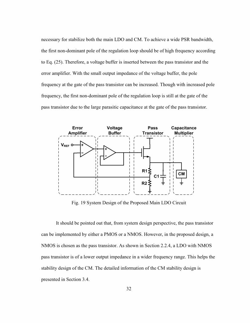
For the voltage buffer design, a two stage voltage follower (M6 and M7) is used
to implement this block. A 2x charge pump (2x CP in Fig. 20) is used to supply the
second stage voltage follower (M7). The charge pump provides a 2.7V supply voltage so
that the second stage voltage follower can drive the gate of the pass transistor to a
voltage higher than the LDO supply voltage (1.8V). This can reduce the drop-out voltage
of the LDO and raise its power efficiency.
There are two reasons for using two stage voltage follower structure. Firstly,
there is a large DC biasing voltage difference between the output voltage of the error
amplifier (~ 0.6V) and the gate drive voltage of the pass transistor (~ 2.3V). Thus,
PMOS voltage follower is suitable for this application because it offers a DC voltage up-
shift and is of low output impedance to work as a voltage buffer. Secondly, the DC
voltage shift value of the voltage follower is proportional to the square root of its DC
biasing current (Eq. (1)). If one stage follower is used, a larger DC biasing current
should be used. Since the output ripple amplitude of the charge pump is proportional to
its output current [15], using larger biasing current for one stage voltage follower can
lead to large ripples and make the LDO’s output noisy. Therefore, the DC voltage shift is
split between the two stage voltage followers.
For the pass transistor, a triple-well NMOS is used as the pass transistor.
Compared with common NMOS which is built in the p-type substrate, triple-well NMOS
is built in an isolated n-type doping well. Therefore, the bulk terminal of the triple-well
NMOS can be wired out. By connecting the bulk terminal to the source terminal, the
triple-well is free from the body effect [9]. This is very useful for designing the LDO
35
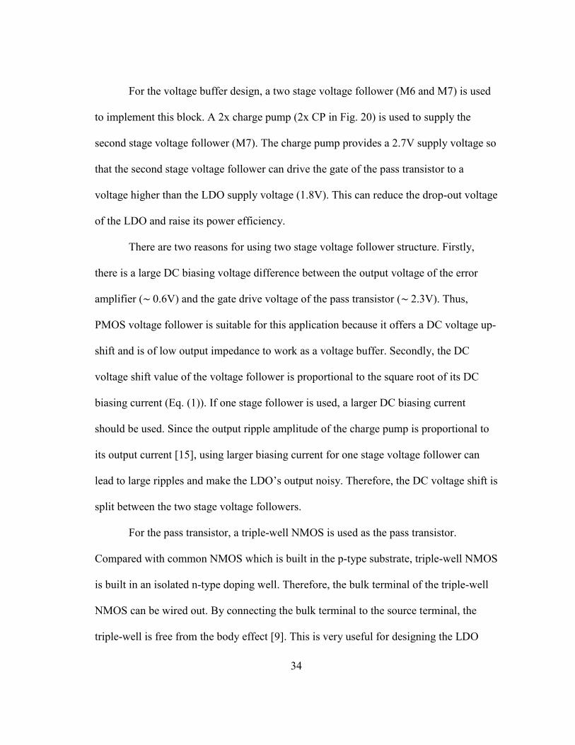
with NMOS pass transistor. For common NMOS pass transistor, its source terminal is
tied to the output node which is over 1.2V, but its bulk terminal is the substrate tied at
ground. This large source-bulk voltage difference creates a threshold voltage increases
over 100mV according to the simulation. This entails the gate drive voltage also increase
100mV to accommodate this higher threshold. Therefore, the voltage room left for the
implementing a good current mirror supplying the voltage follower is reduced and the
design difficulty gets increased.
For conciseness, the circuit design for the current source in the two voltage
follower is not presented in Fig. 20. They are implemented as a self-cascode current
source [16] and shown in Fig. 21. As discussed in Section 2.5.4, the main design criteria
for these current source is to provide high output impedance for attenuating the ripples
from supply and the charge pump. A detailed analysis of this current source and its
effect on the PSR of the whole LDO system is addressed in Section 3.3.
2x CP
CM
Ibias2
R1
R2C1
M6
MP
Triple-Well
Ibias3
M7
M8
M9 M11
M10
IREF1 IREF2
M12
M13
M14
M15
EA
Fig. 21 Self-Cascode Current Sources in the Voltage Followers
36
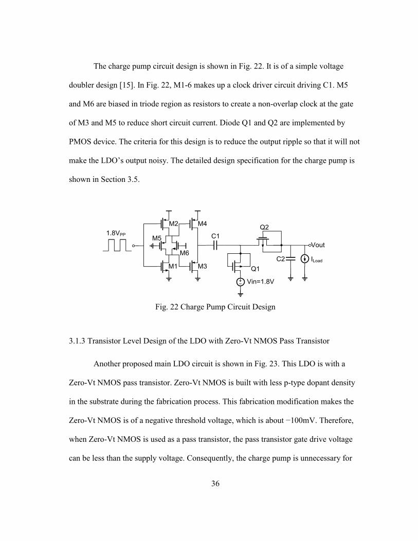
The charge pump circuit design is shown in Fig. 22. It is of a simple voltage
doubler design [15]. In Fig. 22, M1-6 makes up a clock driver circuit driving C1. M5
and M6 are biased in triode region as resistors to create a non-overlap clock at the gate
of M3 and M5 to reduce short circuit current. Diode Q1 and Q2 are implemented by
PMOS device. The criteria for this design is to reduce the output ripple so that it will not
make the LDO’s output noisy. The detailed design specification for the charge pump is
shown in Section 3.5.
Vin=1.8V
M1
M2
M3
M4
M5
M6
C1
C2
Q1
Q21.8VPP
Vout
ILoad
Fig. 22 Charge Pump Circuit Design
3.1.3 Transistor Level Design of the LDO with Zero-Vt NMOS Pass Transistor
Another proposed main LDO circuit is shown in Fig. 23. This LDO is with a
Zero-Vt NMOS pass transistor. Zero-Vt NMOS is built with less p-type dopant density
in the substrate during the fabrication process. This fabrication modification makes the
Zero-Vt NMOS is of a negative threshold voltage, which is about −100mV. Therefore,
when Zero-Vt NMOS is used as a pass transistor, the pass transistor gate drive voltage
can be less than the supply voltage. Consequently, the charge pump is unnecessary for

37
the LDO with Zero-Vt NMOS. Also, the DC voltage shift required from the voltage
follower is reduced for using Zero-Vt NMOS. Thus in the LDO with Zero-Vt NMOS,
the voltage buffer is implemented with one voltage follower. As for the error amplifier,
the circuit is of the same design as the one in the LDO with triple-well NMOS.
Error
Amplifier
Voltage
Buffer
Pass
Transistor
VREF
M1 M1
M2 M2
M4 M4
CMM3
Ibias1
Ibias2
R1
R2C1
M5 M5
M6
MP
Zero-Vt
Capacitance
Multiplier
Fig. 23 Proposed LDO Transistor Level Design with Zero-Vt NMOS
The disadvantage of using the Zero-Vt NMOS pass transistor is its large parasitic
capacitance. Due to the modified fabrication process, the minimum channel length of the
Zero-Vt NMOS (700nm) is much longer than the triple-well NMOS (180nm) in the
0.18µm technology. Therefore, the with the same aspect ratio, the area for using Zero-Vt
NMOS is of about 16 times of a triple-well NMOS. This gives larger capacitance at its
gate node. Thus more current should be used to increase the pole frequency at its gate
node to maintain LDO’s stability. Also, the PSR bandwidth is also reduced due to this
drawback.

38
3.2 Capacitance Multiplier Design
3.2.1 Capacitance Multiplier Introduction
Capacitance multiplier (CM) is a circuit using a small real capacitor to create a
large equivalent capacitance. For capacitors on-chip, they are implemented by parallel
metal plate, whose capacitance is proportional to the area occupied. The on-chip
capacitance density is relatively small (~ 2fF/µm2). Therefore, to save valuable on-chip
area, CM is a practical option to create large capacitance with smaller area occupation.
Current
SensingCurrent
Amplifier
Cc
Current Feedback (M x IC1)
ICc
Vin
Iin M1
(W/L)
M2
(M x W/L)
Ibias M x IbiasCc
(a) (b)
XVin
Fig. 24 Concept of Current Mode CM (a) and Simplified Design of Current Mode CM
Proposed in [17] (b)
The concept and a typical design of the current mode CM proposed in [17] is
shown in Fig. 24. The concept of such a CM (Fig. 24 (a)) contains a current sensing and
a current amplifier block. The current sensing block is used to sense the current going
through Cc and generate a signal reflecting the sensed current ICc. Then the current
amplifier receives this signal, generates a current of M times ICc and feedback it to the
input port of the CM. Thereby, the total current going into the input port is (M+1)ICc.

39
This makes the input equivalent capacitances increases to (M+1)Cc. A typical circuit
which can realize this idea is a current mirror, as shown in Fig. 24 (b). The diode
connected M1 is of low input impedance to sense the current going through Cc at low
frequency. This current signal (ICc) is transformed into the gate drive voltage of M1 and
M2. Thus an M times amplified current will be produced by M2 for the DC biasing
current ratio between M2 and M1 is M. Shunting this current to the input port, the
current mirror creates a circuit of input capacitance (M+1)Cc.
However, there are two main drawbacks avoiding the design in Fig. 24 (b) to be
used to externally compensate a LDO: 1) Large multiplication factor is needed for a CM
to externally compensate a LDO, but for the design in Fig. 24(b), the multiplication
factor totally depends on the DC bias current ratio of the current mirror. Therefore, this
design needs a lot of DC biasing current to realize large amplification factor. This will
degrade the power efficiency of the whole LDO system; 2) the working bandwidth of the
CM in Fig. 24(b) is limited by the pole frequency at node X, which is gm1/Cc according
to [17]. Therefore, to realize a CM with working bandwidth over 10MHz and with a Cc
of tens of pF, the bias current required for M1 (Ibias) goes over 100µA. This leads to the
total current consumption of a 100x CM over 1mA. This again degrades the LDO’s
power efficiency.
To avoid the problems mentioned above, an improved CM circuit is proposed in
this thesis to realize large amplification factor and wide working bandwidth without
consuming too much current. The detailed design description and analysis is presented in
the following section.

40
3.2.1 System Level Design of the CM
M1
M2Cc
A2
M3
A1
M4
Ibias1
Ibias2
CEQ
Current
Sensing
Voltage
Mode
Amplifier
Current
Mode
Amplifier
X
Fig. 25 System Level Design of the Proposed CM
The block diagram of the proposed CM is presented in Fig. 25. Comparing with
the design in Fig.24 (b), in the current sensing block, amplifier with gain A1 is inserted
between the drain and gate node of M1. This amplifier boosts the input conductance at
node X to A1∙gm1. Through this modification, the CM’s sensing bandwidth gets boosted
A1 times without wasting too much current. Between the current sensing block and
current mode amplifier block, an amplifier with gain A2 is inserted. This is a small signal
voltage amplifier amplifying the gate driving voltage of M1. Thus the current amplifying
factor from M4 is boosted to A1∙gm4/gm1. A voltage follower (M2) is added to drive
another PMOS M3 to realize the Class-AB property of the current output stage. This
modification is used because the CM should be able to both sink and source the transient
41
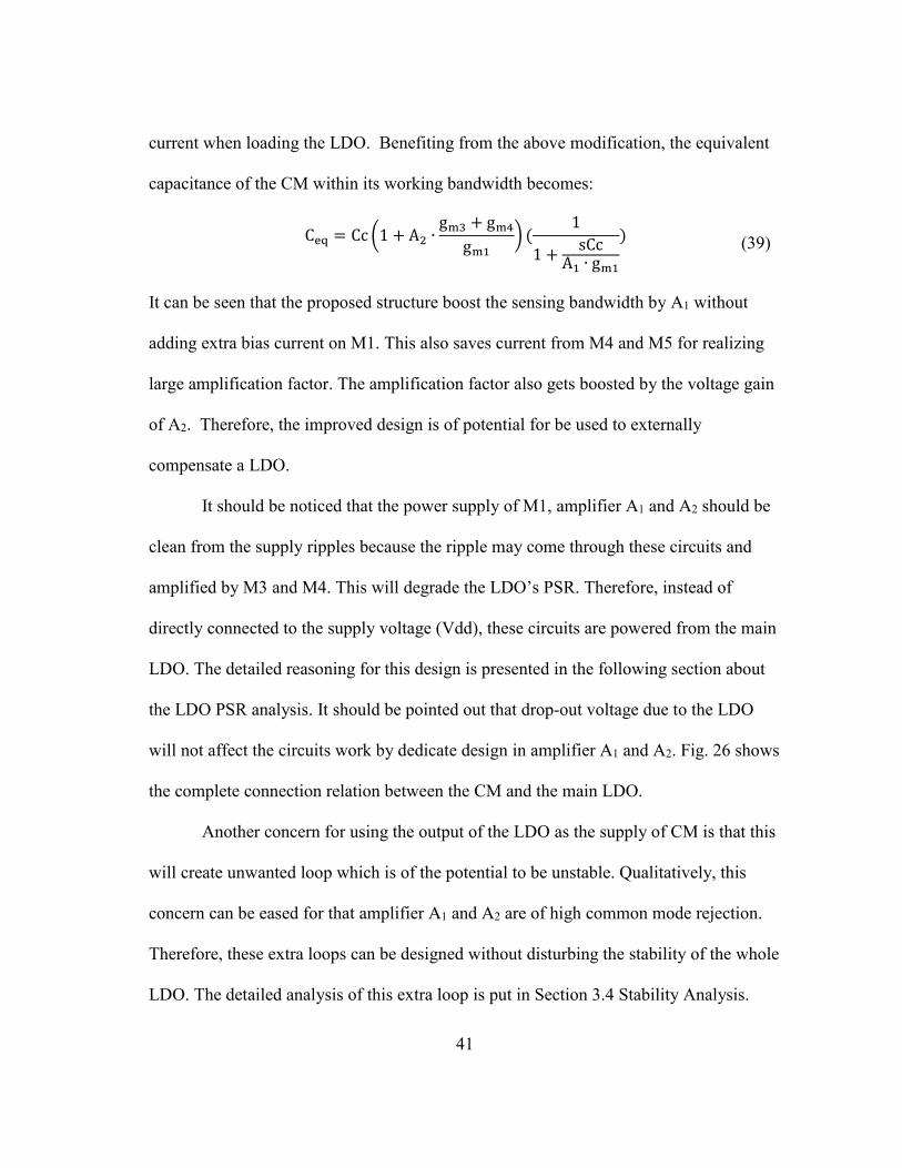
current when loading the LDO. Benefiting from the above modification, the equivalent
capacitance of the CM within its working bandwidth becomes:
Ceq = Cc (1 + A2 ∙
gm3 + gm4gm1
) (1
1 +sCc
A1 ∙ gm1
) (39)
It can be seen that the proposed structure boost the sensing bandwidth by A1 without
adding extra bias current on M1. This also saves current from M4 and M5 for realizing
large amplification factor. The amplification factor also gets boosted by the voltage gain
of A2. Therefore, the improved design is of potential for be used to externally
compensate a LDO.
It should be noticed that the power supply of M1, amplifier A1 and A2 should be
clean from the supply ripples because the ripple may come through these circuits and
amplified by M3 and M4. This will degrade the LDO’s PSR. Therefore, instead of
directly connected to the supply voltage (Vdd), these circuits are powered from the main
LDO. The detailed reasoning for this design is presented in the following section about
the LDO PSR analysis. It should be pointed out that drop-out voltage due to the LDO
will not affect the circuits work by dedicate design in amplifier A1 and A2. Fig. 26 shows
the complete connection relation between the CM and the main LDO.
Another concern for using the output of the LDO as the supply of CM is that this
will create unwanted loop which is of the potential to be unstable. Qualitatively, this
concern can be eased for that amplifier A1 and A2 are of high common mode rejection.
Therefore, these extra loops can be designed without disturbing the stability of the whole
LDO. The detailed analysis of this extra loop is put in Section 3.4 Stability Analysis.

42
M1
M2
Cc
A2
M3
A1
M4
Ibias1
Ibias2
C1
Main LDO
A
Fig. 26 Proposed CM and Its Connection to the Main LDO
3.2.2 Transistor Level Design of the CM.
In this section, to maintain clearness and conciseness, the transistor level design
of the CM is presented from block to block.
Fig. 27 shows the transistor level design of amplifier A1 in the CM. In the
proposed design, A1 is implemented by a two-stage amplifier (M5-7). This two stage
amplifier offers a gain 40dB.
The small signal voltage amplifier (amplifier A2) is implemented by a simple
positive gain amplifier (M8-11) as shown in Fig. 28. One design issue for this amplifier
is that it can suffer from large DC output voltage variation due to process variation. This
can interfere the DC biasing of the output stage (M2-4). Therefore, another regulating
amplifier (M12-16) is added to cancel the DC offset.

43
M1
M2Cc
A2
M3
M4
Ibias1Ibias2
C1
Main LDO
M5
M6 M6
M5
M7
Ibias3 Ibias4
Vb1
A1
Fig. 27 Transistor Level Implementation of Amplifier A1 in CM
From the system level perspective, the amplifier A2 is of the structure as an
output offset amplifier in [9]. This structure is reproduced in Fig. 31. In this structure,
AG is the amplifier made up of transistor M8-11 in Fig. 30 and can be taken as an
amplifier providing voltage mode gain. In the design, the output regulating amplifier can
be taken as a transconductance amplifier (gm-reg). The offset voltage of at the output of
AG (VOS-AG) is suppressed by the gain of the transconductance amplifier and the small
signal amplifier:
VOS−out =
VOS−AG1 + AG ∙ gm−reg ∙ rout−reg
(40)
With the high gain provided by these two amplifiers (AG and gm-reg∙rout-reg), the DC
output voltage of the amplifier A2 in CM can be taken as the bias voltage at the input of
the regulating amplifier (Vb2 in Fig. 28).
44
M1
M2
Cc
M3
A1
M4
Ibias1
C1
Main LDO
M8
Vb2
M12
M13 M13
M14 M14
M16 M16
M15
M9 M10
M11
M12 M15
C2
A2
Ibias5
Ibias2
Fig. 28 Transistor Level Implementation of Amplifier A2 in CM
Vout
Cout-reg
rout-reg
AG
gm-reg
Vin
VOS-AG
Fig. 29 Amplifier with Output Offset Cancellation in [9]
The regulating amplifier’s working frequency should be limited to avoid
attenuate the small signal which should be amplified. Therefore, a large capacitor C2 is
added to limit the working frequency of the auxiliary regulating amplifier in A2. In this
design, C2 is of 80pF and the working frequency range for the whole small signal
amplifier is from 100kHz to 100MHz. The detailed frequency response of the small
signal amplifier will be shown in Section 4, which is about the LDO’s simulation results.

45
3.3 System PSR Analysis
To design a LDO with good PSR, each circuit component should be inspected
because each of them, if connected to Vdd, can introduce supply ripples to the LDO
output. In this section, the PSR analysis of both the main LDO and the CM is provided.
Simulation results are also provided for helping understanding of the analysis.
3.3.1 PSR Analysis of the Main LDO
3.3.1.1 PSR Analysis of the Main LDO with Triple Well NMOS
In the LDO with triple-well NMOS, there are three paths connected to Vdd and
introducing supply ripples to the LDO output (Vout). These three paths are illustrated in
Fig.30. They are: 1) Path 1 through the EA to Vout; 2) Path 2 through the supply of the
first stage voltage follower to the output of the Vout; 3) Path 3 through the supply of the
pass transistor channel resistance to Vout.
VREF
M1 M1
M2 M2
M4 M4
2x CP
CMM3
Ibias1
Ibias2
R1
R2C1
M5 M5
M6
MP
Triple-WellIbias3
M7
Path 1
Path 2
Path 3
Vout
Fig. 30 Paths in the LDO with Triple-Well Introducing Supply Ripples to Vout

46
Theoretically, these three paths all contributes to the feed-forward supply ripple
gain described in Eq. (15). Denoting the gain of these three paths as AFF,EA (Path 1),
AFF,VF (Path 2) and AFF,MP (Path 3), the sum of these three paths is the total supply ripple
feed-forward gain of the main LDO:
AVin(s) = AFF,EA(s) + AFF,VF(s) + AFF,MP(s) (41)
The channel resistance of the pass transistor is inversely proportional to its drain
current [9]. This effect is modeled by the equation:
rds−MP =
1
λIDS−MP (42)
in which λ is the channel length modulation effect coefficient. According to Eq. (42), the
channel resistance of the pass transistor reach its minimum value when the LDO is
providing the maximum loading current. With the minimized channel resistance, the
pass transistor’s supply noise shielding effect is minimized. Therefore, in the full load
current case, the pass transistor (Path 3 in Fig. 30) is the dominant path through which
the supply ripple comes to the output of the LDO.
When the load current of the LDO is in the minimum condition, the channel
resistance of the pass transistor becomes very large, as described in Eq. (42). In this case,
the path through the error amplifier becomes the dominant path introducing supply
ripple. Therefore, in light load current case, the PSR of the proposed LDO is mainly
determined by the PSR contributed by the error amplifier. In the design, the PSR due to
these three paths in different loading condition (Iout = 10mA, 1mA and 0.1mA) is
simulated. The simulation results are shown in Fig. 31, 32 and 33. The simulation results
match the point mentioned above.
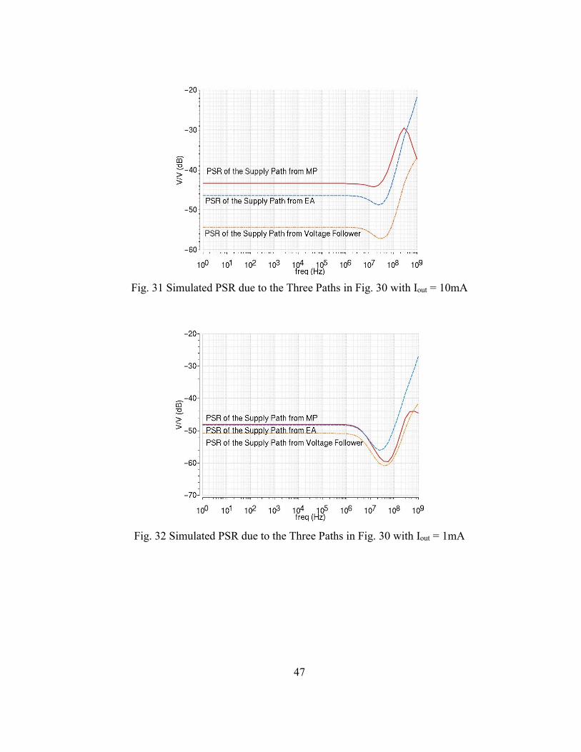
47
Fig. 31 Simulated PSR due to the Three Paths in Fig. 30 with Iout = 10mA
Fig. 32 Simulated PSR due to the Three Paths in Fig. 30 with Iout = 1mA

48
Fig. 33 Simulated PSR due to the Three Paths in Fig. 30 with Iout = 0.1mA
3.3.1.2 PSR Analysis of the Main LDO with Zero-Vt NMOS
VREF
M1 M1
M2 M2
M4 M4
CMM3
Ibias1
Ibias2
R1
R2C1
M5 M5
M6
MP
Zero-Vt
Path 3Path 2Path 1
Vout
Fig. 34 Paths in the LDO with Zero-Vt Introducing Supply Ripples to Vout
The three paths contributing to the PSR of the LDO with Zero-Vt NMOS is
labeled out in Fig. 34. Same to the LDO with triple-well NMOS pass transistor, the path
transistor is the dominant PSR contributing path in heavy load current case, while the
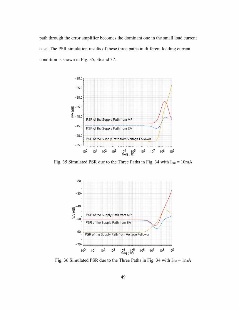
49
path through the error amplifier becomes the dominant one in the small load current
case. The PSR simulation results of these three paths in different loading current
condition is shown in Fig. 35, 36 and 37.
Fig. 35 Simulated PSR due to the Three Paths in Fig. 34 with Iout = 10mA
Fig. 36 Simulated PSR due to the Three Paths in Fig. 34 with Iout = 1mA
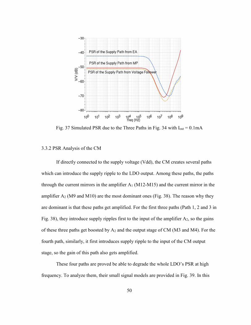
50
Fig. 37 Simulated PSR due to the Three Paths in Fig. 34 with Iout = 0.1mA
3.3.2 PSR Analysis of the CM
If directly connected to the supply voltage (Vdd), the CM creates several paths
which can introduce the supply ripple to the LDO output. Among these paths, the paths
through the current mirrors in the amplifier A1 (M12-M15) and the current mirror in the
amplifier A2 (M9 and M10) are the most dominant ones (Fig. 38). The reason why they
are dominant is that these paths get amplified. For the first three paths (Path 1, 2 and 3 in
Fig. 38), they introduce supply ripples first to the input of the amplifier A2, so the gains
of these three paths get boosted by A2 and the output stage of CM (M3 and M4). For the
fourth path, similarly, it first introduces supply ripple to the input of the CM output
stage, so the gain of this path also gets amplified.
These four paths are proved be able to degrade the whole LDO’s PSR at high
frequency. To analyze them, their small signal models are provided in Fig. 39. In this

51
figure, gmx and rdsx denote the transcondutance and the channel resistance of transistor
Mx; Areg and rout-reg denote the DC gain and the output impedance of the output offset
regulating amplifier in the amplifier A2; A1,1 and A1,2 denote the gain of the first and
second stage of the amplifier A1.
M1
M2
Cc
M3
M4
Ibias2
M5
M6 M6
M5
M7
A1
M10
M8
M9
M11
C2
A2
Areg
Main LDO
M13 M14 M15M12
Ibias2
C1
ZOUT-LDO
Path 1 Path 2 Path 3 Path 4
Fig. 38 Four Critical Paths in the CM Affecting PSR of the LDO
gm5(rds5||rds6) gm7(rds7||rds11)
gm1(rds1||rds13||Cc)
gm6rds14
1 rds7
rds7 + rds15
A1
rds1||Ccrds13 + (rds1||Cc)
Vdd
Path 1 Path 2 Path 3
gm3 + gm4
ZOUT-LDO
Vout
rds10
rds10 + rds11
Path 4
gm8
gm4
rds10 || rds11
AP1 AP2 AP3 AP4
A1,2A1,1
A2
Areg
1+sC2rout-reg
Fig. 39 Small Signal Model of the Critical Paths in Fig. 38

52
From the small signal model in Fig. 39, it can be concluded that the PSR due to
the CM, PSRCM, can be described by the following equations:
PSRCM(s) =
(
AF,A1
1 +ALoop,A1
1 +s
ωp,A1
+AP4
1 +ALoop,A2
1 +s
ωp,A2)
(gm3 + gm4) ∙ ZOUT−LDO
≈ (
AF,A1 (1 +s
ωp,A1)
ALoop,A1+
AP4 (1 +s
ωp,A2)
ALoop,A2) ∙ (gm3 + gm4) ∙ ZOUT−LDO
(43)
AF,A1 = (AP1 ∙ A1 + AP2 ∙ A1,1 + AP3) ∙ A2 (44)
ωp,A1 =
1
(rds1||rds13) ∙ Cc (45)
ALoop,A1 = A1 ∙ gm1 ∙ (rds1||rds13) (46)
ωp,A2 =
1
rout−AUX ∙ C2 (47)
ALoop,A2 = AAUX ∙ gm8 ∙ (rds10||rds11) (48)
From the above equation, it can be seen that the PSRCM is of high-pass frequency
response. This is because the four paths labeled in Fig. 38 are all regulated by a local
loop. For Path 1, 2 and 3, they are regulated by the loop of A1 and M1. For Path 4, it is
regulated by the loop of the auxiliary amplifier in A2 and M11. These two local loops
are of high gain (ALoop,A1 in Eq. (46) and ALoop,A2 in Eq. (47)) so that, at low frequency,
the supply ripple introduced by these four paths is greatly suppressed. However, since
the dominant poles of these two loops are at low frequency due to the large capacitance
of Cc and C2, the four critical paths start to increase their gain due to the gain loss

53
caused by the low frequency poles in the local loops. Mathematically, these two poles
turns out to be zeroes in the PSRCM transfer function as shown in Eq. (43) and lead to
PSRCM increase.
Theoretically, the PSR of the whole LDO system, PSRtot, should be equal to the
sum of the PSR due to the main LDO, PSRLDO, and the PSR due to the CM, PSRCM.
Ideally, PSRCM should be much smaller than PSRLDO so that PSRtot is approximately
equal to PSRLDO and the proposed LDO possesses the exact same PSR character as those
of external capacitors. However, as shown in Eq. (43), PSRCM can be very large at high
frequency due to the low frequency zeroes. If PSRCM is larger than the PSRLDO at high
frequency, the PSR bandwidth of the whole LDO system will be degraded by the CM.
To prevent this PSR degradation, in the proposed design, the supply voltage of
the amplifier A1 and A2 in the CM is changed from Vdd to the LDO output (Vout). The
detailed transistor level connection of this modification is shown in Fig. 40. As labeled
out by the red line, the supply connections of the amplifier A1 and A2 are modified from
Vdd to Vout.
M1
M2
Cc
M3
M4
Ibias2
M5
M6 M6
M5
M7
Vb1
A1
M10
M8
M9
M11Vb2
C2
A2
AAUX
Main LDO
M13 M14 M15M12
Ibias1
C1
Fig. 40 Modified Connection Relation between the Main LDO and the CM
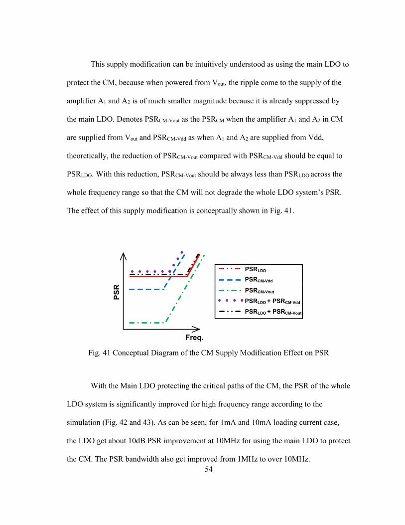
54
This supply modification can be intuitively understood as using the main LDO to
protect the CM, because when powered from Vout, the ripple come to the supply of the
amplifier A1 and A2 is of much smaller magnitude because it is already suppressed by
the main LDO. Denotes PSRCM-Vout as the PSRCM when the amplifier A1 and A2 in CM
are supplied from Vout and PSRCM-Vdd as when A1 and A2 are supplied from Vdd,
theoretically, the reduction of PSRCM-Vout compared with PSRCM-Vdd should be equal to
PSRLDO. With this reduction, PSRCM-Vout should be always less than PSRLDO across the
whole frequency range so that the CM will not degrade the whole LDO system’s PSR.
The effect of this supply modification is conceptually shown in Fig. 41.
PSRLDO
PSRCM-Vdd
Freq.
PS
R PSRCM-Vout
PSRLDO + PSRCM-Vout
PSRLDO + PSRCM-Vdd
Fig. 41 Conceptual Diagram of the CM Supply Modification Effect on PSR
With the Main LDO protecting the critical paths of the CM, the PSR of the whole
LDO system is significantly improved for high frequency range according to the
simulation (Fig. 42 and 43). As can be seen, for 1mA and 10mA loading current case,
the LDO get about 10dB PSR improvement at 10MHz for using the main LDO to protect
the CM. The PSR bandwidth also get improved from 1MHz to over 10MHz.

55
Fig. 42 Simulation of PSR with and without Main LDO Protection for CM at 1mA
Loading Current
Fig. 43 Simulation of PSR with and without Main LDO Protection for CM at 10mA
Loading Current
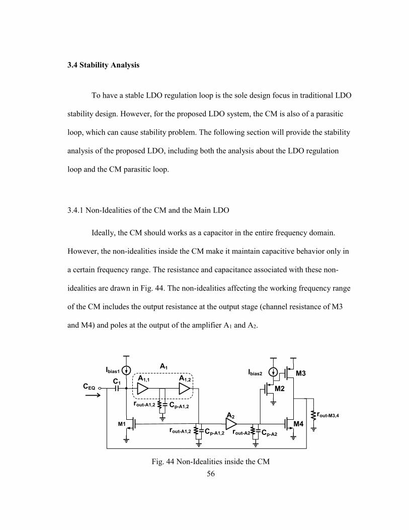
56
3.4 Stability Analysis
To have a stable LDO regulation loop is the sole design focus in traditional LDO
stability design. However, for the proposed LDO system, the CM is also of a parasitic
loop, which can cause stability problem. The following section will provide the stability
analysis of the proposed LDO, including both the analysis about the LDO regulation
loop and the CM parasitic loop.
3.4.1 Non-Idealities of the CM and the Main LDO
Ideally, the CM should works as a capacitor in the entire frequency domain.
However, the non-idealities inside the CM make it maintain capacitive behavior only in
a certain frequency range. The resistance and capacitance associated with these non-
idealities are drawn in Fig. 44. The non-idealities affecting the working frequency range
of the CM includes the output resistance at the output stage (channel resistance of M3
and M4) and poles at the output of the amplifier A1 and A2.
M1
M2C1
A2
M3A1,2
M4
Ibias1 Ibias2
CEQ
rout-M3,4
Cp-A2rout-A2Cp-A1,2rout-A1,2
A1,1
Cp-A1,2rout-A1,2
A1
Fig. 44 Non-Idealities inside the CM

57
The finite output resistance of M3 and M4 (rout-M3,4) affects only the low
frequency behavior of the CM because it only adds a parallel resistance at CM output.
The poles at the output of amplifier A1 and A2 are at relatively high frequency for small
parasitic capacitance associated with them. They can make the CM behave as an
inductor at high frequency. This can be observed by including these poles into Eq. (39)
and modify it as the equivalent admittance equation of the CM (excluding rout-M3,4):
Yeq−CM = sCc(1 +A2
1 +s
ωpA2
gm3 + gm4gm1
)
(
1
1 +sCcA1gm1
(1 +s
ωpA1,1) (1 +
sωpA1,2
))
≈ sCc(A2
1 +s
ωpA2
∙gm2 + gm3gm1
)(1
1 +sCc
A1 ∙ gm1∙ (1 +
sωpA1,1
) (1 +s
ωpA1,2))
(49)
In the above equation, ωpA1,1 and ωpA1,2 denotes the first and second stage of the
amplifier A1 output pole frequencies. ωpA2 denotes the amplifier A2 output pole
frequency. Eq. (49) shows that the poles from the amplifiers turn out to be poles in the
Yeq-CM. These poles make Yeq-CM decrease beyond their frequencies. Therefore, the CM
becomes inductive at high frequency. The simulation result of the Yeq-CM (Fig. 45)
proves this point: at low frequency (0-10kHz), the CM is resistive due to the output
resistance of M3 and M4; at the middle frequency (30kHz-30MHz), the CM works as a
capacitor for its admittance increases with frequency; at high frequency (30MHz~), the
CM works as an inductor for its admittance decreases with frequency.

58
Ad
mit
tan
ce
(s
)
Fig. 45 Simulation Results of the Output Admittance of the CM
As for the LDO, the non-ideality of it, which affects the stability design, also lies
in the LDO’s output impedance. Ideally, the small signal output impedance of a LDO
should be resistive and extremely small because the LDO should exhibit small voltage
variation when load current varies. For an ideal LDO with NMOS pass transistor, its
output impedance is:
Zout =gm−MP1 + AEA
(50)
However, the parasitic poles inside the regulation loop, which are the error
amplifier output pole at ωpEA and voltage follower output pole at ωpVF, can turn this
pure resistive output impedance into an inductive one:
Zout =gm−MP
1 +AEA
(1 +s
ωpEA)(1 +
sωpVF
)
(51)

59
This inductive behavior can be intuitively understood as, when the LDO regulation loop
gain decreases due to the parasitic poles inside it, the output impedance of the LDO
increases (Eq. (51)). This behavior is like an inductor, which increase its impedance as
the frequency increases. For the proposed main LDO structure, their output impedance is
simulated and the results are shown in Fig. 46.
Fig. 46 Output Impedance of the Proposed Main LDO
From the above analysis, it can be seen that the parasitic poles inside the LDO
and the CM makes them behaves like an inductor at high frequency. This causes the
problem that they may extend each other’s unity gain frequency (UGF) of the loop gain
frequency response. The extended UGF can cover more parasitic poles so that the phase
marge of the loop get reduced. This stability issue is discussed in the following section.

60
3.4.2 Analysis of the Main LDO Stability
VREF
CMR1
R2
Regulation Loop
PEA
PVF
Zout-CM
MP
Fig. 47 Regulation Loop of Proposed Main LDO
The regulation loop of the proposed main LDO circuit is shown in Fig. 47, in
which pEA and pVF denote the output pole of the error amplifier and the voltage follower.
For analysis simplicity, the resistance of the feedback network (R1+R2) is neglected for
it is much larger than the channel resistance of the pass transistor (rds-MP). Assuming the
voltage follower is of unity DC gain, denoting the error amplifier DC gain as AEA, and
CM equivalent output impedance as Zout-CM, the transfer function of the regulation loop
gain is formulated as follows:
ALoop(s) =
AEA
1 +s
ωpEA
∙1
1 +s
ωpVF
∙gm−MP ∙ (rds−MP||Zout−CM )
1 + gm−MP ∙ (rds−MP||Zout−CM ) (52)
For ideal CM of equivalent capacitance CL, the third term in Eq. (52), which is
the voltage gain from NMOS pass transistor, AMP(s), becomes:
AMP(s) =
gm−MP ∙ (rds−MP||sCL )
1 + gm−MP ∙ (rds−MP||sCL)≈
1
1 + sCL/ gm−MP (53)
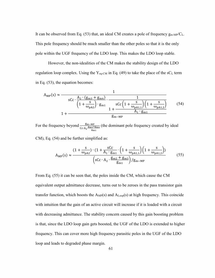
61
It can be observed from Eq. (53) that, an ideal CM creates a pole of frequency gm-MP/CL.
This pole frequency should be much smaller than the other poles so that it is the only
pole within the UGF frequency of the LDO loop. This makes the LDO loop stable.
However, the non-idealities of the CM makes the stability design of the LDO
regulation loop complex. Using the Yeq-CM in Eq. (49) to take the place of the sCL term
in Eq. (53), the equation becomes:
AMP(s) ≈1
1 +
sCc ∙A2 ∙ (gm3 + gm4)
(1 +s
ωpA2) ∙ gm1
∙1
1 +sCc (1 +
sωpA1,1
) (1 +s
ωpA1,2)
A1 ∙ gm1gm−MP
(54)
For the frequency beyond gm−MP
Cc∙A2∙gm3+gm4gm1
(the dominant pole frequency created by ideal
CM), Eq. (54) and be further simplified as:
AMP(s) ≈
(1 +s
ωpA2) ∙ (1 +
sCcA1 ∙ gm1
∙ (1 +s
ωpA1,1) (1 +
sωpA1,2
))
(sCc ∙ A2 ∙gm2 + gm3gm1
) /gm−MP (55)
From Eq. (55) it can be seen that, the poles inside the CM, which cause the CM
equivalent output admittance decrease, turns out to be zeroes in the pass transistor gain
transfer function, which boosts the AMP(s) and ALoop(s) at high frequency. This coincide
with intuition that the gain of an active circuit will increase if it is loaded with a circuit
with decreasing admittance. The stability concern caused by this gain boosting problem
is that, since the LDO loop gain gets boosted, the UGF of the LDO is extended to higher
frequency. This can cover more high frequency parasitic poles in the UGF of the LDO
loop and leads to degraded phase margin.

62
To suppress this unwanted gain increase, as mentioned earlier, a real on-chip
capacitor C1 is added at the output node of the LDO. From admittance perspective, the
real capacitor is of larger admittance than the CM at high frequency so that it can shunt
the gain boosting effect caused by the decreasing CM admittance. Therefore, the LDO
loop gain is reduced by this C1 instead of being raised by the CM at high frequency. In
the design, a C1 of 600pF is used. In the simulation, the output conductance of the CM
and the C1 of 600pF are compared (Fig. 48). It can be seen that C1 dominates the
conductance over the CM beyond frequency about 90MHz.
Capacitance Multiplier
Capacitor C1 (600pF)
Frequency C1 Start to Dominate
Ou
tpu
t A
dm
itta
nce (
s)
Fig. 48 Output Admittance of the CM and Real Capacitor
The effect of this non-ideality of CM on the loop gain of the LDO is shown in
Fig. 49 and 50. Fig. 49 presents the loop gain of the LDO with triple-well NMOS. In the
simulation, the loop gain is measured in the cases when the LDO is loaded with a real
capacitor of similar output capacitance (4.5nF) of the CM, the LDO is loaded only with
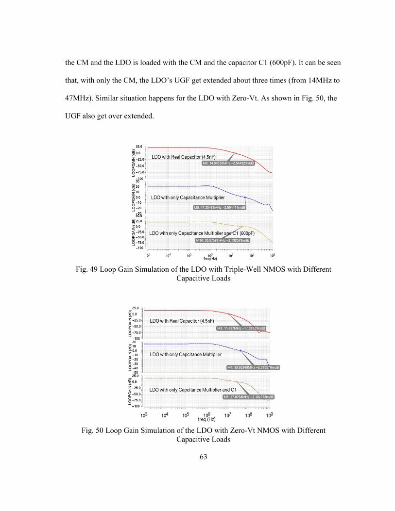
63
the CM and the LDO is loaded with the CM and the capacitor C1 (600pF). It can be seen
that, with only the CM, the LDO’s UGF get extended about three times (from 14MHz to
47MHz). Similar situation happens for the LDO with Zero-Vt. As shown in Fig. 50, the
UGF also get over extended.
Fig. 49 Loop Gain Simulation of the LDO with Triple-Well NMOS with Different
Capacitive Loads
Fig. 50 Loop Gain Simulation of the LDO with Zero-Vt NMOS with Different
Capacitive Loads

64
3.4.3 Analysis of the CM Stability
Ideally the CM is expected to be of only open-loop behavior. That means it only
senses the signal out of its own circuit but not the signal generated by itself. However,
there is a parasitic loop embedded within the proposed CM which can cause instability
problem. This parasitic loop is labeled out in Fig. 51.
M1
M2C1
A2
M3
A1
M4
Ibias1
Ibias2
C1
Main LDO
Zout-LDO
CM Parasitic Loop
Y
Fig. 51 CM Parasitic Loop
At low frequency, the capacitor Cc blocks the current signal generated in the
current amplifier stage (M2-4) from going back to the current sensing block (M1 and
amplifier A1) for its high impedance. The main LDO is also of very low input impedance
so that all the current signals goes into the main LDO. However, as the frequency
increases, the output impedance of the main LDO increases (Fig. 46) and the impedance
of Cc decreases. Therefore, a fraction of the current generated in the current amplifying
stage goes back to the current sensing stage and forming the parasitic loop.
To analysis the loop gain of the CM connected to the LDO, the parasitic loop can
be divided into two segments. The first segment starts at node Y in Fig. 51 and ends at

65
the output of amplifier A1. In this segment, voltage signal at node Y is transferred into
the gate drive voltage of M1 (output of amplifier A1). The second segment starts at the
input of amplifier A2 and ends at node Y. In this segment, the voltage signal at the output
of A1 gets amplified by A2. The amplified voltage signal is transformed into current
signal by M3 and M4. Then the output current of M3 and M4 goes into node Y. With
finite node impedance at node X, this current signal is reflected as a voltage signal at
node Y. For simplicity, in the analysis of the second segment, the effect of the regulation
amplifier in amplifier A2 is ignored. This is because the regulation amplifier only affects
low frequency response of the amplifier A2 but the UGF of the CM’s parasitic loop is of
much higher frequency.
The transfer function of the parasitic loop of the CM is described by equations:
ALoop−CM = G1(s) ∙ G2(s) (56)
G1(s) =
sCc
gm1(1 +sCc
A1(s) ∙ gm1)
(57)
A1(s) =
A1
(1 +s
ωpA1,1) ∙ (1 +
sωpA1,1
)
(58)
G2(s) =
A2
(1 +s
ωpA2)∙ (gm3 + gm4) ∙ Zin−LDO (59)
Zout−LDO =
(1 +s
ωpEA) (1 +
sωpVF
)
gm−MP ∙ AEA
(60)
In Eq. (56), G1 and G2 denote the gain of the first and second segment in the CM
loop. In Eq. (57), A1(s) is the transfer function of amplifier A1 in the CM. In Eq. (58),
66
ωpA1,1and ωpA1,1denotes the two parasitic pole frequencies at the first and second stage
of the amplifier A1. In Eq. (59), ωpA2 stands for the pole frequency at the output of A2
excluding the effect of the regulation amplifier. In Eq. (60), AEA denotes the DC gain of
the error amplifier and ωpEA and ωpVF denotes the parasitic pole frequencies at the
output of the error amplifier and the voltage follower in the main LDO.
Combining Eq. (56)-(60), a complete CM loop gain transfer function is:
ALoop(s) = sCc
gm1(1 +sCc
A1(s)gm1)∙A2 ∙ (gm3 + gm4)(1 + s/ωpEA)(1 + s/ωpEA)
gm−MP ∙ AEA ∙ (1 + s/ωpA2) (61)
Realizing the term A2∙(gm3+gm4)
gm1 is the amplification factor of the CM and denote it as
ACM, Eq. (61) can be simplified as:
ALoop(s) = ACM ∙
sCc
1 +sCc
A1(s) ∙ gm1
∙(1 + s/ωpEA)(1 + s/ωpEA)
gm−MP ∙ AEA ∙ (1 + s/ωpA2) (62)
Including the two parasitic poles of A1 into Eq. (62), the loop gain becomes:
ALoop(s) = ACM ∙sCc
1 +sCc (1 +
sωpA1,1
) (1 +s
ωpA1,2)
A1 ∙ gm1
∙
(1 +s
ωpEA) (1 +
sωpVF
)
gm−MP ∙ AEA ∙ (1 +s
ωpA2)
(63)
Since Cc is a large capacitor (40pF), it is reasonable to assume the pole frequency,
A1∙gm1/Cc, is smaller than the other poles and zeroes. Therefore, for frequency larger
than the pole frequency A1∙gm1/Cc, Eq. (63) can be simplified as:
ALoop(s) =ACM ∙ A1 ∙ gm1gm−MP ∙ AEA
∙
(1 +s
ωpEA) (1 +
sωpVF
)
(1 +s
ωpA1,1) (1 +
sωpA1,2
) (1 +s
ωpA2)
(64)

67
From Eq. (64) it can be seen that the CM is of high stability risk when the loading
current of the main LDO is small and gm-MP is small. In the small loading current case,
the loop is of high gain so that poles with frequency ωpA1,1, ωpA1,2and ωpA2 can come
into the UGF of the loop and reduce the phase margin of the loop. Moreover, the poles
of the main LDO turn out to be zeroes for the loop of the CM. These zeroes can further
boost the gain of the CM loop and overly extend the UGF of the CM.
To avoid the over large UGF of the CM loop, as shown in Fig.53, capacitor C1 is
added to shunting the main LDO. Therefore, at high frequency, capacitor C1 is of lower
impedance than the main LDO output impedance so that C1 can attenuate the CM UGF
extension effect caused by the main LDO. In the proposed design, a capacitor around
600pF is used as C1. The CM’s loop gain frequency response is simulated when the
external loading current for the main LDO is 100µA. The simulation results are shown
in Fig. 52 and 53. As can be seen from the simulation results, without C1, the CM’s
UGF can be of over 1GHz. With that high UGF, even the poles without considered in
Eq. (64) come into the UGF and the phase margin for the loop is a negative number. By
adding C1, the UGF of the CM loop is limited within 100MHz and the phase margin of
the loop is about 70o.
Another stability concern of the CM loop is that there are some other paths not
being considered in Eq. (64). These paths are created by using the LDO’s output as the
supply of the amplifier A1 and A2 in the CM. These paths are indicated in Fig. 54.
Though they intersect with the CM loop but they are of much smaller gain comparing to
the main path. In the simulation, the loop gain of the CM include and exclude these

68
paths are simulated. The loop gain frequency responses are shown in Fig. 55. It can be
seen that these extra paths do not seemingly modify the loop frequency response.
Fig. 52 Simulation of the CM Loop Frequency Response with Triple-Well LDO with
and without C1
Fig. 53 Simulation of the CM Loop Frequency Response with Zero-Vt LDO with and
without C1
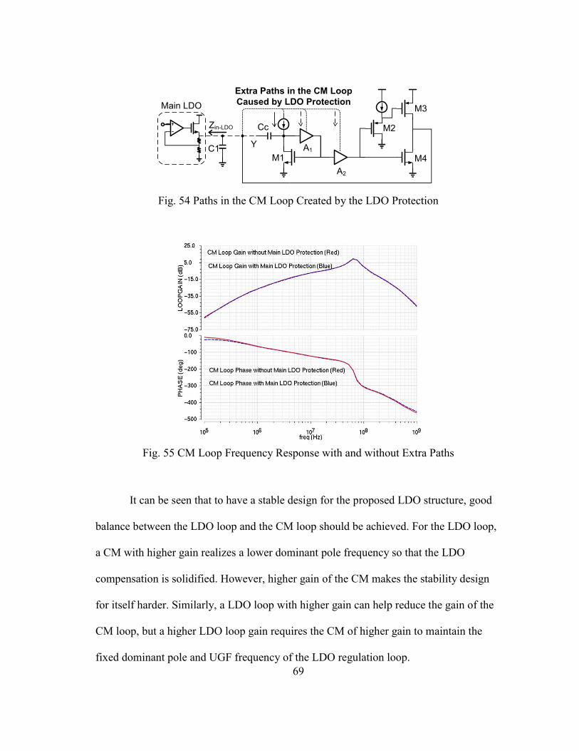
69
M1
M2Cc
A2
M3
A1
M4C1
Main LDO
Zin-LDO
Y
Extra Paths in the CM Loop
Caused by LDO Protection
Fig. 54 Paths in the CM Loop Created by the LDO Protection
Fig. 55 CM Loop Frequency Response with and without Extra Paths
It can be seen that to have a stable design for the proposed LDO structure, good
balance between the LDO loop and the CM loop should be achieved. For the LDO loop,
a CM with higher gain realizes a lower dominant pole frequency so that the LDO
compensation is solidified. However, higher gain of the CM makes the stability design
for itself harder. Similarly, a LDO loop with higher gain can help reduce the gain of the
CM loop, but a higher LDO loop gain requires the CM of higher gain to maintain the
fixed dominant pole and UGF frequency of the LDO regulation loop.

70
3.5 Design Flexibility
In this part, the flexibility of the proposed main LDO circuit to work with lower
supply voltage and the flexibility of the CM to implement different output capacitance
values are investigated. This investigation is valuable because it reflects the feasibility of
the proposed LDO structure being implemented by smaller technology with lower
supply voltage and the feasibility of the CM working with LDOs with different
maximum output current. These design flexibilities is important for modifying the
proposed design to fit into different applications.
In the following context, the supply voltage limit and the scalability of the CM
are discussed to reveal the flexibility of the proposed design.
3.5.1 Minimum Supply Voltage of the Main LDO Structure
Theoretically, both the output voltage range of the error amplifier and the voltage
buffer can limit the supply range of the main LDO. However, the output voltage range of
the error amplifier can be easily modified and accommodated by the level shifter by
changing level shifter’s bias current. Therefore, the minimum supply voltage is limited
by the output voltage range of the level shifter connected to the pass transistor. In the
proposed main LDO with triple-well NMOS, as shown in Fig. 56, the minimum supply
voltage requirement comes into the scenario when the load current reach the maximum
value. In this case, the over drive voltage of the pass transistor reaches its maximum
value as described in Eq. (1). Since the LDO output voltage is relatively fixed, the gate
voltage of the pass transistor reaches its maximum value. Therefore, the voltage across

71
the biasing current source of the second stage voltage follower (Ibias3) reaches its
minimum value for realizing the maximum gate voltage. For Ibias3 implemented by a
current mirror which requires a minimum voltage drop Vdsat-Ibias3, the voltage difference
between the charge pump output voltage and the maximum pass transistor gate voltage
should be larger than Vdsat-Ibias3 to maintain the proper working of the voltage shifter.
VREF
M1 M1
M2 M2
M4 M4
2x CP
CM
M3
Ibias1
Ibias2
R1
R2
C1
M5 M5
M6
MP
Triple-WellIbias3
M7Vgs-MP
Vdsat-Ibias3
Iout = IMAX
Fig. 56 Supply Voltage Limit of the Main LDO with Triple-Well NMOS
The above voltage limit can be expressed by the following equation (Vout-CP
denotes the output voltage of the charge pump):
Vout−CP − (Vout + Vgs−MP|IMAX ) ≥ Vdsat−Ibias3 (65)
In the proposed design, Vout-CP ≈ 1.5 Vdd. Therefore, the minimum supply
voltage can be expressed as:
Vdd ≥ ( Vdsat−Ibias3 + Vout + Vgs−MP|IMAX )/1.5 (66)
Similar reasoning can be applied to the main LDO with Zero-Vt NMOS. As
shown in Fig. 57, the minimum supply voltage is still limited in the scenario when the
load current reaches its maximum value.
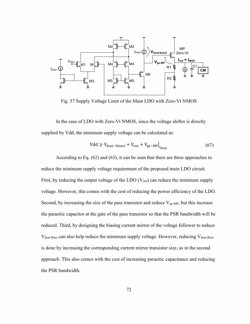
72
VREF
M1 M1
M2 M2
M4 M4
M3
Ibias1
Ibias2
R1
R2M5 M5
M6
MP
Zero-Vt
CMC1
Iout = IMAX
Vdsat-Ibias2
Vgs-MP
Fig. 57 Supply Voltage Limit of the Main LDO with Zero-Vt NMOS
In the case of LDO with Zero-Vt NMOS, since the voltage shifter is directly
supplied by Vdd, the minimum supply voltage can be calculated as:
Vdd ≥ Vdsat−Ibias2 + Vout + Vgs−MP|IMAX (67)
According to Eq. (62) and (63), it can be seen that there are three approaches to
reduce the minimum supply voltage requirement of the proposed main LDO circuit.
First, by reducing the output voltage of the LDO (Vout) can reduce the minimum supply
voltage. However, this comes with the cost of reducing the power efficiency of the LDO.
Second, by increasing the size of the pass transistor and reduce Vgs-MP, but this increase
the parasitic capacitor at the gate of the pass transistor so that the PSR bandwidth will be
reduced. Third, by designing the biasing current mirror of the voltage follower to reduce
Vdsat-Ibias can also help reduce the minimum supply voltage. However, reducing Vdsat-Ibias
is done by increasing the corresponding current mirror transistor size, as in the second
approach. This also comes with the cost of increasing parasitic capacitance and reducing
the PSR bandwidth.
73
3.5.2 Scalability of the CM to Implement Different Capacitor Values
According to Eq. (39), there are three ways to modify the equivalent output
capacitance of the CM. First of all, by modifying the capacitor being amplified (Cc in
Fig. 25), the output equivalent capacitance of the capacitor multiplier can be changed.
Secondly, modifying the size and the biasing current of the CM output stage (M3 and
M4 in Fig. 25) can change the equivalent output capacitance of the CM. Thirdly,
changing the gain of the small signal voltage amplifier (A2 in Fig. 25) can change the
equivalent capacitance.
To realize a larger output capacitance, the above three methods come with
different costs. For the first method, using larger capacitor consumes more on-chip area.
Moreover, since the frequency A1∙gm1/Cc is the CM capacitive working bandwidth
according to Eq. (39), the bandwidth of the CM will be reduced if using larger capacitor.
For the second approach, increasing the size of the output stage of the CM will reduce
the pole frequency at the output of the small signal amplifier (A2 in Fig. 25). According
to Eq. (51), this also raises the stability risk of the LDO it compensated. Moreover, this
method also raises the current consumption. For the third approach, the basic way of
increasing the gain of the small signal voltage amplifier is to use longer transistor.
Similar to the second approach, this reduces the pole frequency at the amplifier output
and make LDO stability design harder.
Based on the above analysis, a suitable way of modifying the output capacitance
of the CM without sacrificing the stability design is that, maintain the biasing voltage
while scale the transistor size of M1-5, M10 and M11 in Fig. 28 with the scale of the

74
capacitor being multiplied. Through this way, the capacitive working bandwidth of the
CM and the pole frequency at the output of the small signal amplifier maintain the same.
Therefore, the output capacitance of the CM is scaled with the minimum disturbance to
the main LDO stability design.
Based on the above method, different output capacitance of the CM multiplier is
implemented in the schematic design scenario. In the simulation, the working bandwidth
of the capacitor multiplier maintains almost the same, the relation between the current
consumption and the equivalent capacitance is shown in Fig. 58. It can be seen that the
output equivalent capacitance of the CM is almost scaled with the current consumption.
This means that, to be applied in the LDO with larger maximum load current, which
requires larger CM equivalent capacitance, more current should be used in the CM.
Fig. 58 Current Consumption and CM Output Equivalent Capacitance
50
100
150
200
250
1 2 3 4 5 6 7 8 9
Cu
rren
t C
on
sum
pti
on
(µA
)
Equivalent Capacitance (nF)
CM Equivalent Capacitance vs Current Consumption

75
3.6 Design Specifications
The main goal of this design is to realize a LDO with −40dB PSR over 10MHz
and maximum load current 10mA. Since NMOS is used as pass transistor, the output
voltage of the LDO is set as 1.2V (Vdrop-out = 0.6V) for the trade-off between the drop-
out voltage and the design complexity of the charge pump for driving the gate of the
pass transistor. A brief design procedure for determining the design parameters of the
LDOs is presented as follows:
1) Determining the minimum size of the pass transistor which can maintain in
saturation in maximum loading current condition (Iout = 10mA).
2) Design the voltage follower to have its output pole at 20MHz.
3) Design the error amplifier to have the PSR of the LDO less than −40dB.
4) Using an ideal capacitor to determine the minimum output capacitance to
make the LDO regulation loop stable.
5) Assuming the CM is of 100x multiplication factor, find out the value of Cc,
which is the capacitor being amplified, to create the capacitance needed to
externally stabilize the LDO regulation loop.
6) Assuming the voltage gain of the amplifier A1 in the CM is 100, design the
M1 in the CM (Fig. 25) to make the pole frequency A1∙gm1/Cc (CM
capacitive working bandwidth) equal to the UGF found in step 4).
7) Design the small signal amplifier and the current amplifying stage of the CM
to realize a 100x multiplication factor.
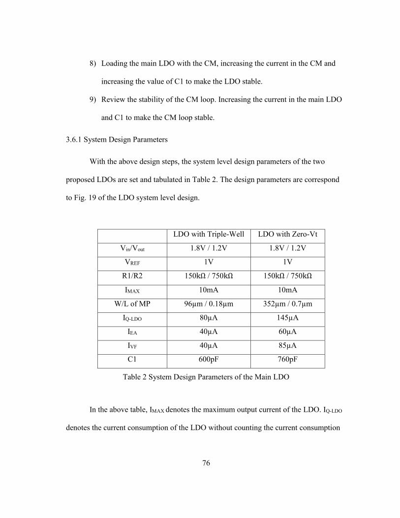
76
8) Loading the main LDO with the CM, increasing the current in the CM and
increasing the value of C1 to make the LDO stable.
9) Review the stability of the CM loop. Increasing the current in the main LDO
and C1 to make the CM loop stable.
3.6.1 System Design Parameters
With the above design steps, the system level design parameters of the two
proposed LDOs are set and tabulated in Table 2. The design parameters are correspond
to Fig. 19 of the LDO system level design.
LDO with Triple-Well LDO with Zero-Vt
Vin/Vout 1.8V / 1.2V 1.8V / 1.2V
VREF 1V 1V
R1/R2 150kΩ / 750kΩ 150kΩ / 750kΩ
IMAX 10mA 10mA
W/L of MP 96µm / 0.18µm 352µm / 0.7µm
IQ-LDO 80µA 145µA
IEA 40µA 60µA
IVF 40µA 85µA
C1 600pF 760pF
Table 2 System Design Parameters of the Main LDO
In the above table, IMAX denotes the maximum output current of the LDO. IQ-LDO
denotes the current consumption of the LDO without counting the current consumption
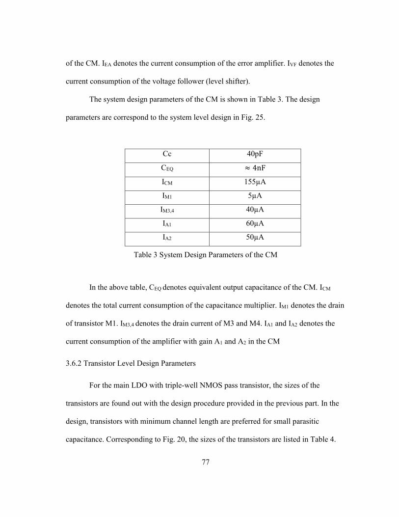
77
of the CM. IEA denotes the current consumption of the error amplifier. IVF denotes the
current consumption of the voltage follower (level shifter).
The system design parameters of the CM is shown in Table 3. The design
parameters are correspond to the system level design in Fig. 25.
Cc 40pF
CEQ ≈ 4nF
ICM 155µA
IM1 5µA
IM3,4 40µA
IA1 60µA
IA2 50µA
Table 3 System Design Parameters of the CM
In the above table, CEQ denotes equivalent output capacitance of the CM. ICM
denotes the total current consumption of the capacitance multiplier. IM1 denotes the drain
of transistor M1. IM3,4 denotes the drain current of M3 and M4. IA1 and IA2 denotes the
current consumption of the amplifier with gain A1 and A2 in the CM
3.6.2 Transistor Level Design Parameters
For the main LDO with triple-well NMOS pass transistor, the sizes of the
transistors are found out with the design procedure provided in the previous part. In the
design, transistors with minimum channel length are preferred for small parasitic
capacitance. Corresponding to Fig. 20, the sizes of the transistors are listed in Table 4.

78
W/L W/L
M1 4.8µm / 0.18µm M2 3µm / 0.54µm
M3 13.2µm / 0.18µm M4 4.8µm / 0.18µm
M5 7.2µm / 0.18µm M6 0.5µm / 0.18µm
M7 1µm / 0.18µm MP 96µm / 0.18µm
Table 4 Transistor Level Design of the LDO with Triple-Well Pass Transistor
For the charge pump design, the main goal is to make the output ripple caused by
charge pump lower than the LDO’s output noise level. According to the simulation, the
integrated output noise (1Hz – 1GHz) of the proposed LDOs is about 1.5mVrms.
Therefore, the supply ripple caused by the charge pump should be less than this value.
With this design goal, corresponding to Fig. 22, the design parameters of the charge
pump are listed in Table 5.
W/L W/L
M1 2.5µm / 0.18µm M2 5µm / 0.18µm
M3 25µm / 0.18µm M4 50µm / 0.18µm
M5 1µm / 0.18µm M6 0.6µm / 0.18µm
Q1 576µm / 0.4µm Q2 576µm / 0.4µm
Value Value
C1 40pF C2 140pF
Table 5 Transistor Level Design of the Charge Pump in the LDO with Triple-Well
For the main LDO with Zero-Vt pass transistor, corresponding to Fig. 23, the
sizes of the transistors are listed in Table 6.

79
W/L W/L
M1 2.5µm / 0.18µm M2 5µm / 0.18µm
M3 25µm / 0.18µm M4 50µm / 0.18µm
M5 1µm / 0.18µm M6 0.6µm / 0.18µm
MP 352µm / 0.18µm
Table 6 Transistor Level Design of the LDO with Zero-Vt Pass Transistor
As for the CM design, corresponding to the circuits shown in Fig. 27 and 28, the
circuit design parameters are tabulated in Table 5.
W/L W/L
M1 0.6µm / 0.18µm M2 0.5µm / 0.18µm
M3 6µm / 0.18µm M4 2.4µm / 0.18µm
M5 1µm / 0.18µm M6 1.2µm / 0.18µm
M7 0.6µm / 0.18µm M8 0.6µm / 0.18µm
M9 0.5µm / 0.18µm M10 2.0µm / 0.18µm
M11 2.4µm / 0.18µm M12 0.6µm / 0.18µm
M13 2.0µm / 0.18µm M14 2.0µm / 0.18µm
M15 0.6µm / 0.18µm M16 0.6µm / 0.18µm
Value Value
Cc 40pF C2 80pF
Table 7 Transistor Level Design of the CM
With the above design parameters, the two LDOs are simulated to make sure
their stability and PSR regulation ability. The detailed simulation results are shown in
the next section.

80
4. SIMULATION RESULTS AND LAYOUT
The two LDOs are designed, layout and simulated in IBM 0.18µm technology. In
the following context, the layout profile, small signal simulation, stability simulation and
transient simulation results are provided to prove the feasibility of the design.
4.1 Layout Profile
The die size of the two proposed LDO is 1.5mm × 1.5mm. The layout profile for
the LDO with triple-well is shown in Fig. 59 and the one for the LDO with Zero-Vt is
shown in Fig. 60. For the LDO with triple-well, the active area is about 0.166mm2
including the area of the charge pump. For the LDO with Zero-Vt, the active area is
about 0.183mm2.
Chare Pump
C1
Cc C2 of A2 in CM
LDO and CM
Fig. 59 Layout Profile of the LDO with Triple-Well

81
C1
CcC2 of A2 in CM
LDO and CM
Fig. 60 Layout Profile of the LDO with Zero-Vt
4.2 Static Small Signal Simulation Results
4.2.1 Capacitance Multiplier
The small signal equivalent admittance of the CM is like a LC series tank in
parallel with a resistors as discussed in Section 3.4. In the simulation, the equivalent
admittance of the CM is compared with such a passive LC and resistor combination
shown in Fig. 61. In the simulation, RP = 33kΩ, C =3.95nF, L= 0.8nH and RS = 1.2Ω. It
can be seen that the CM is equivalent to such a network from about 400kHz to 140MHz.
RP
C
RS
L
YEQ
Fig. 61 Small Signal Equivalent Network of the CM
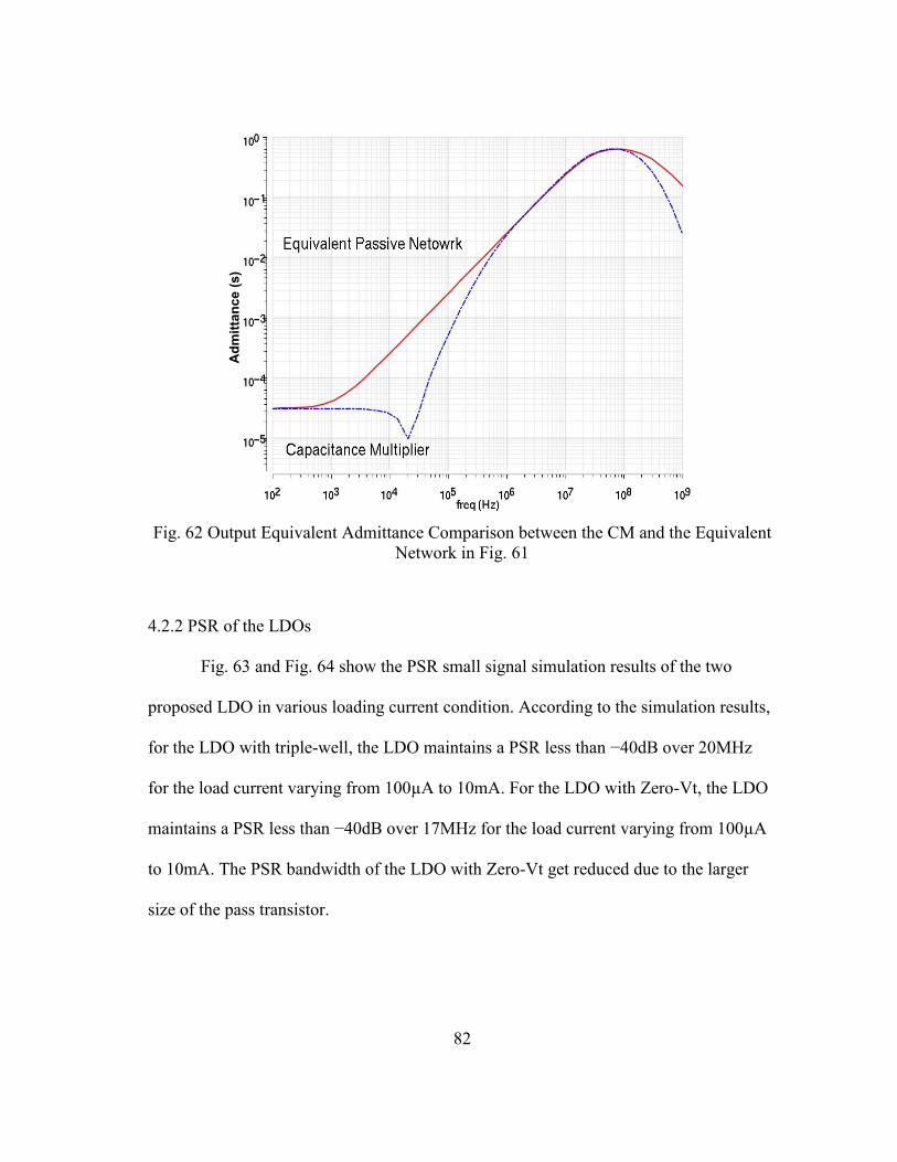
82
Ad
mit
tan
ce
(s
)
Fig. 62 Output Equivalent Admittance Comparison between the CM and the Equivalent
Network in Fig. 61
4.2.2 PSR of the LDOs
Fig. 63 and Fig. 64 show the PSR small signal simulation results of the two
proposed LDO in various loading current condition. According to the simulation results,
for the LDO with triple-well, the LDO maintains a PSR less than −40dB over 20MHz
for the load current varying from 100µA to 10mA. For the LDO with Zero-Vt, the LDO
maintains a PSR less than −40dB over 17MHz for the load current varying from 100µA
to 10mA. The PSR bandwidth of the LDO with Zero-Vt get reduced due to the larger
size of the pass transistor.
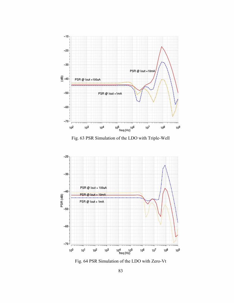
83
Fig. 63 PSR Simulation of the LDO with Triple-Well
Fig. 64 PSR Simulation of the LDO with Zero-Vt
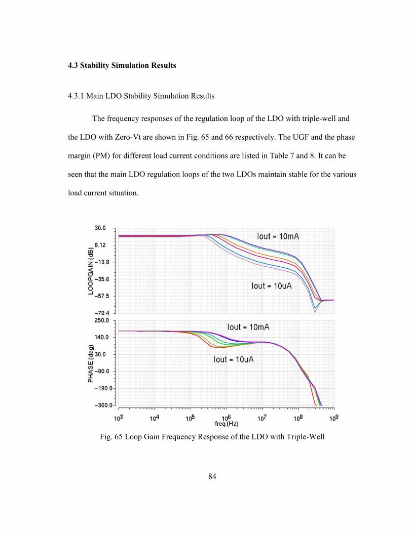
84
4.3 Stability Simulation Results
4.3.1 Main LDO Stability Simulation Results
The frequency responses of the regulation loop of the LDO with triple-well and
the LDO with Zero-Vt are shown in Fig. 65 and 66 respectively. The UGF and the phase
margin (PM) for different load current conditions are listed in Table 7 and 8. It can be
seen that the main LDO regulation loops of the two LDOs maintain stable for the various
load current situation.
Fig. 65 Loop Gain Frequency Response of the LDO with Triple-Well
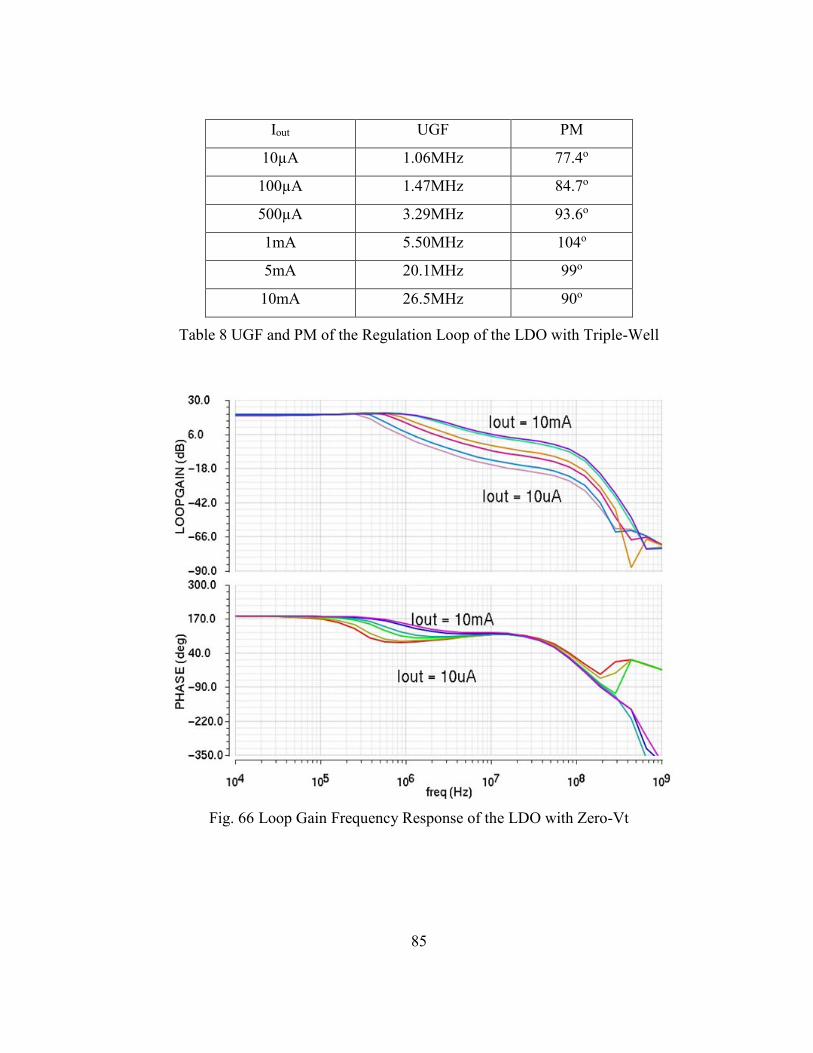
85
Iout UGF PM
10µA 1.06MHz 77.4o
100µA 1.47MHz 84.7o
500µA 3.29MHz 93.6o
1mA 5.50MHz 104o
5mA 20.1MHz 99o
10mA 26.5MHz 90o
Table 8 UGF and PM of the Regulation Loop of the LDO with Triple-Well
Fig. 66 Loop Gain Frequency Response of the LDO with Zero-Vt

86
Iout UGF PM
10µA 1.06MHz 85.4o
100µA 1.47MHz 89.3o
500µA 3.29MHz 96.0o
1mA 5.50MHz 103o
5mA 20.1MHz 108o
10mA 26.5MHz 103o
Table 9 UGF and PM of the Regulation Loop of the LDO with Zero-Vt
4.3.2 CM Stability Simulation Results
The frequency responses of the CM parasitic loop are shown in Fig. 67 and 68.
Fig. 67 presents the case when the CM is connected to the LDO with triple-well pass
transistor and Fig. 68 presents the case when the CM is connected to the LDO with Zero-
Vt pass transistor. The corresponding UGF and PM of the two cases are recorded and
tabulated in Table 9 and 10. From the simulation results it can be seen, as discussed in
Section 3.4.3, adding a real capacitor (C1 in Fig. 51) shunting the LDO output prevents
the UGF of the CM loop from being too large so that the CM loop is of a bad PM. In the
simulation, the maximum UGF of the CM is limited around 100MHz and the PM is over
55o across the loading current from 10µA to 100mA.

87
Fig. 67 CM Loop Frequency Response When Connected to LDO with Triple-Well
UGF PM
10µA 65.4MHz 78.9o
100µA 67.0MHz 78.5o
500µA 74.5MHz 76.2o
1mA 81.2MHz 73.4o
5mA 97.1MHz 60.9o
10mA 100.6MHz 55.6o
Table 10 UGF and PM of the CM Loop Connected to the LDO with Triple-Well
88
Fig. 68 CM Loop Frequency Response When Connected to LDO with Zero-Vt
UGF PM
10µA 65.4MHz 85.7o
100µA 67.0MHz 86.3o
500µA 74.5MHz 83.3o
1mA 81.2MHz 78.5o
5mA 97.1MHz 62.7o
10mA 100.6MHz 55.0o
Table 11 UGF and PM of the CM Loop Connected to the LDO with Zero-Vt
89
4.4 Transient Simulation Results
4.4.1 LDO Transient Simulation Results
In this part, simulation is implemented to test the stability of the LDOs when they
are facing the practical large signals. In the simulation, the load transient is simulated
with a current pulse switching between 10µA and 10mA. The line transient is simulation
with a supply pulse switching between 1.6V and 2.0V for 100µA, 1mA and 10mA
loading current cases. The detailed simulation results are shown in Fig. 69-80.
According to the simulation, for the LDO with triple-well, the output voltage variation
due to the current step is about 40mV and the output voltage variation due to the supply
step is about 4mV. For the LDO with Zero-Vt, the output voltage variation due to the
current step is about 30mV and the output variation due to the supply step is about 4mV.
Fig. 69 Load Transient of the LDO with Triple-Well
90
Fig. 70 Transient Response of the LDO with Triple-Well for a Current Step Up
Fig. 71 Transient Response of the LDO with Triple-Well for a Current Step Down
91
Fig. 72 Line Transient Response of the LDO with Triple Well for Iout = 10mA
Fig. 73 Line Transient Response of the LDO with Triple Well for Iout = 1mA
92
Fig. 74 Line Transient Response of the LDO with Triple Well for Iout =100µA
Fig. 75 Load Transient of the LDO with Zero-Vt
93
Fig. 76 Transient Response of the LDO with Zero-Vt for a Current Step Up
Fig. 77 Transient Response of the LDO with Zero-Vt for a Current Step Down
94
Fig. 78 Line Transient Response of the LDO with Zero-Vt for Iout = 10mA
Fig. 79 Line Transient Response of the LDO with Zero-Vt for Iout = 1mA

95
Fig. 80 Line Transient Response of the LDO with Zero-Vt for Iout = 100µA
For the charge pump, the output ripple of it is about 20mV. The ripple at the
output of the LDO caused by the charge pump is about 0.03mV. This is less than the
output noise of the LDO (1.5mV). The simulation result is shown in Fig. 81.
Fig. 81 Transient Simulation Results of the Charge Pump and LDO Output

96
4.4.2 CM Transient Simulation Results
To test the CM’s transient behavior, it is disconnected from the main LDO and
connected to a sinusoidal voltage source. Applying a 1MHz, 100mVPP at the input of the
CM, the input current of the CM is measured in the simulation. The transient simulation
result is shown in Fig. 82. Comparing with a 4nF ideal capacitor, it can be seen that the
maximum output current for the CM is about 1mA.
Fig. 82 Transient Simulation Result of the CM
97
5. EXPERIMENTAL RESULTS
The two proposed LDOs are fabricated in IBM 0.18µm technology and packaged
in a QFN 16-pin 4mm × 4mm chip package. A test PCB board is designed and built for
testing the two LDOs. In the test, two LDOs are tested through load regulation, line
regulation, load transient, line transient and PSR test. The measuring method and the test
results are presented in the following context. In the end of this part, a table summarizing
the test results is provided.
5.1 Testing PCB Board Design
In the test board, circuits generating the desired reference voltages and currents
are built for the chip under test. A simplified test board schematic is shown in Fig 83.
CM
R1
R2
MP
EA
VSW
LDOREF3
LDOREF1
VREF
LDOREF2 BJT1 BJT2
MSW
RT1
RT2
LDO Chip
Test Board
Signal
Generator
DC Power
SourceBias Tee
50Ohm
Fig. 83 Simplified Schematic of the PCB Test Board

98
Three TI TPS76201 LDOs (LDOREF 1, 2, 3) are used in the test board to provide
the bias voltages in need. LDOREF1 provides the reference voltage of the LDO under
tested. LDOREF2 and potentiometer RT1 combines together to works as a current source to
provide the bias current needed on board. It should be noticed that in the real board,
multiple potentiometers are used to provide different biasing currents for the chip. One
NXP PMP4501V containing one 1:1 matched current mirror (BJT1 and 2) is used to
provide the loading current of the LDO under test. LDOREF3 and potentiometer RT2 are
used to provide the bias current for the current mirror. A MOSFET switch MSW is
inserted between the RT2 and BJT2. This switch is used for testing the LDO’s load
transient response. In the loading transient test, a square wave switch signal VSW is
switched between 0V and 5V to turn on and off the switch. Then a transient load current
between 10µA and 10mA is created. For static testing case, VSW is biased at 5V to make
the switch always close.
To test the LDOs’ PSR, a Bias-Tee is used to couple the AC sinusoidal wave to
the DC supply voltage. A 50Ω resistor shunts from the supply to the ground is used for
the impedance matching for the signal generator. The photograph of the implemented
test board is shown in Fig. 84.

99
Fig. 84 PCB Test Board
5.2 Testing Results
The two proposed LDOs are characterized by measuring their load regulation,
line regulation, load transient response, line transient response and PSR. For measuring
the load regulation, the LDOs’ output voltage is measured with respect to different load
currents. For the line regulation, the LDOs’ output voltage is measured with different
supply voltage and different load currents. For the load and line transient response, the
output transient voltage is measured with respect to the load current and supply voltage
step. The PSR is measured by comparing the supply ripple amplitude and output ripple
tone magnitude at the frequency of the supply ripple. The detailed results are shown in
the following paragraphs.

100
5.2.1 Test Results of the LDO with Triple-Well NMOS
5.2.1.1 Load and Line Regulation
In this part, the load current is set from 10µA to 10mA. The output voltage
variation is shown in Fig. 85. It can be seen that the for the load current varying from
10µA to 10mA, the output voltage of the LDO with triple-well NMOS pass transistor
varies from about 1.25V to 1.19V.
Fig. 85 Load Regulation of the LDO with Triple-Well
For the line regulation testing, the supply voltage (Vdd) varies from 1.4V to
2.4V. The corresponding output voltages are measured and the results are shown in
Fig.86. For the case when load current is 100µA, it can be seen that the LDO loses its
regulation ability when the supply voltage is higher than 2.1V and the LDO’s output
voltage deviates over 100mV to 1.2 V.
1.19
1.2
1.21
1.22
1.23
1.24
1.25
1.26
0.00 2.00 4.00 6.00 8.00 10.00
Vo
ut(V
)
Load Current (mA)
LDO with Triple-Well Load Regulation

101
Fig. 86 Line Regulation of the LDO with Triple-Well
5.2.1.2 Load and Line Transient
To test the load transient response, a voltage step from 0V to 5V with 50ns rise
and fall time is applied at the gate of the switch (MSW) in Fig. 83. When the switch is
open, the load current of the LDO is 10µA and when the switch is closed is closed, the
load current is 10mA. The test results are shown in Fig. 87. According to the simulation,
the settling time for the LDO with triple-well is about 200ns when the load current is
switched between 10µA and 10mA. The output voltage variation due to the load current
step is about 42mV.
1.17
1.18
1.19
1.2
1.21
1.22
1.23
1.24
1.25
1.26
1.27
1.3 1.5 1.7 1.9 2.1 2.3 2.5
Vo
ut(V
)
Vdd (V)
LDO with Triple-Well Line Regulation
Iout = 10mA
Iout = 1mA
Iout = 100uA
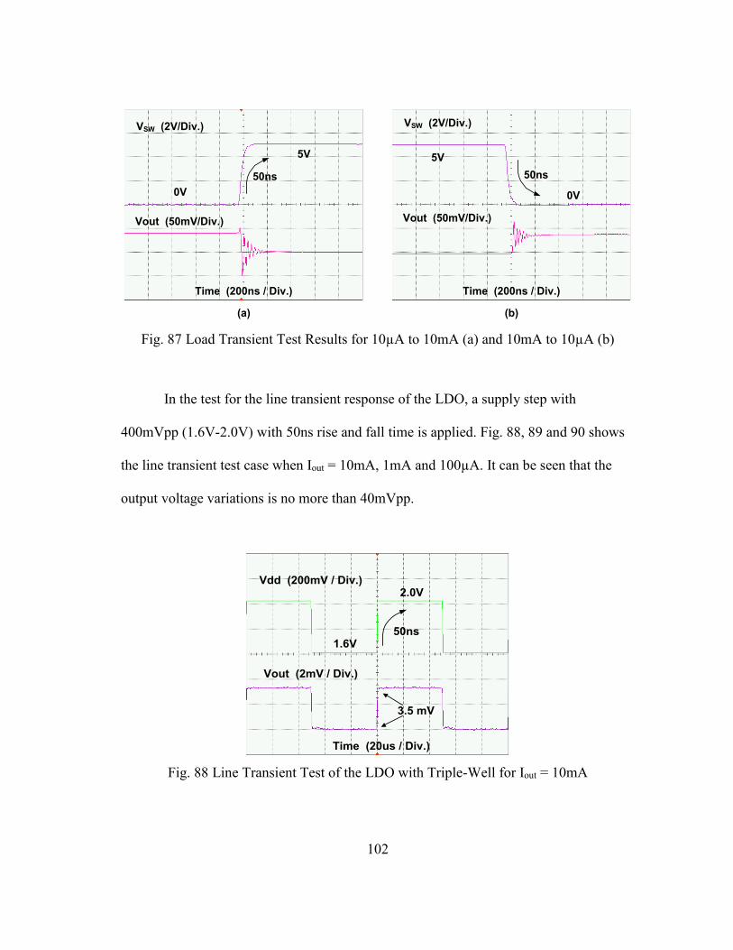
102
Time (200ns / Div.) Time (200ns / Div.)
VSW (2V/Div.)
0V
5V
50ns 50ns
5V
0V
VSW (2V/Div.)
Vout (50mV/Div.) Vout (50mV/Div.)
(a) (b)
Fig. 87 Load Transient Test Results for 10µA to 10mA (a) and 10mA to 10µA (b)
In the test for the line transient response of the LDO, a supply step with
400mVpp (1.6V-2.0V) with 50ns rise and fall time is applied. Fig. 88, 89 and 90 shows
the line transient test case when Iout = 10mA, 1mA and 100µA. It can be seen that the
output voltage variations is no more than 40mVpp.
Vdd (200mV / Div.)
Vout (2mV / Div.)
1.6V
2.0V
50ns
Time (20us / Div.)
3.5 mV
Fig. 88 Line Transient Test of the LDO with Triple-Well for Iout = 10mA
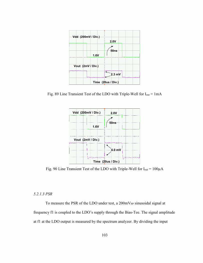
103
Vdd (200mV / Div.)
1.6V
2.0V
50ns
Vout (2mV / Div.)
Time (20us / Div.)
2.3 mV
Fig. 89 Line Transient Test of the LDO with Triple-Well for Iout = 1mA
Vdd (200mV / Div.)
1.6V
2.0V
50ns
Vout (2mV / Div.)
4.0 mV
Time (20us / Div.)
Fig. 90 Line Transient Test of the LDO with Triple-Well for Iout = 100µA
5.2.1.3 PSR
To measure the PSR of the LDO under test, a 200mVPP sinusoidal signal at
frequency f1 is coupled to the LDO’s supply through the Bias-Tee. The signal amplitude
at f1 at the LDO output is measured by the spectrum analyzer. By dividing the input

104
signal and output signal amplitude, the PSR at frequency f1 is measured. The measured
results are shown in Fig. 88. From the results it can be seen that the worst case PSR
happens when the load current is 10mA. In this case, the LDO maintains a −40dB PSR
to 19 MHz.
Fig. 91 PSR Test Results of the LDO with Triple-Well
5.2.1.4 Charge Pump Test Results
This test is executed to verify that the charge pump in the LDO does not
introduce too much noise at the output of the LDO. The transient response of the charge
pump is first measured and it can be seen that the output ripple of the charge pump is
about 20mVpp. The charge pump’s output wave form is then compared with the LDO’s
output. It can be seen that in the time domain there is no significant LDO output ripples
correlated to the charge pump’s output ripple. This results are shown in Fig. 92. To
-60
-50
-40
-30
-20
-10
1.0E+3 1.0E+4 1.0E+5 1.0E+6 1.0E+7 1.0E+8
PSR
(d
B)
Frequency (Hz)
PSR of LDO with Triple Well
Iout=10mA
Iout=7mA
Iout=4mA
Iout=1mA
Iout=500uA
Iout=100uA

105
further verify the insignificant noise effect of the charge pump, the LDO’s output is
sampled at 100MHz. FFT analysis of the 20000 sampled output voltage is applied. It can
be seen that, at 10MHz, which is the charge pump’s working frequency, the tone
amplitude is about -106dB. This is correspond to an 11µVpp signal. The FFT analysis
results are shown in Fig. 93.
CLK (1V / Div.)
Charge Pump Output (20mV / Div.)
LDO Vout (4mV / Div.)
Time (200ns / Div.)
Fig. 92 Time Domain Charge Pump Output and LDO’s Output
Fig. 93 FFT Analysis of the LDO Output Voltage
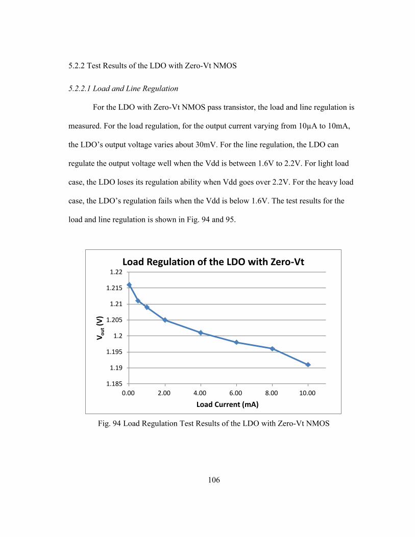
106
5.2.2 Test Results of the LDO with Zero-Vt NMOS
5.2.2.1 Load and Line Regulation
For the LDO with Zero-Vt NMOS pass transistor, the load and line regulation is
measured. For the load regulation, for the output current varying from 10µA to 10mA,
the LDO’s output voltage varies about 30mV. For the line regulation, the LDO can
regulate the output voltage well when the Vdd is between 1.6V to 2.2V. For light load
case, the LDO loses its regulation ability when Vdd goes over 2.2V. For the heavy load
case, the LDO’s regulation fails when the Vdd is below 1.6V. The test results for the
load and line regulation is shown in Fig. 94 and 95.
Fig. 94 Load Regulation Test Results of the LDO with Zero-Vt NMOS
1.185
1.19
1.195
1.2
1.205
1.21
1.215
1.22
0.00 2.00 4.00 6.00 8.00 10.00
Vo
ut
(V)
Load Current (mA)
Load Regulation of the LDO with Zero-Vt
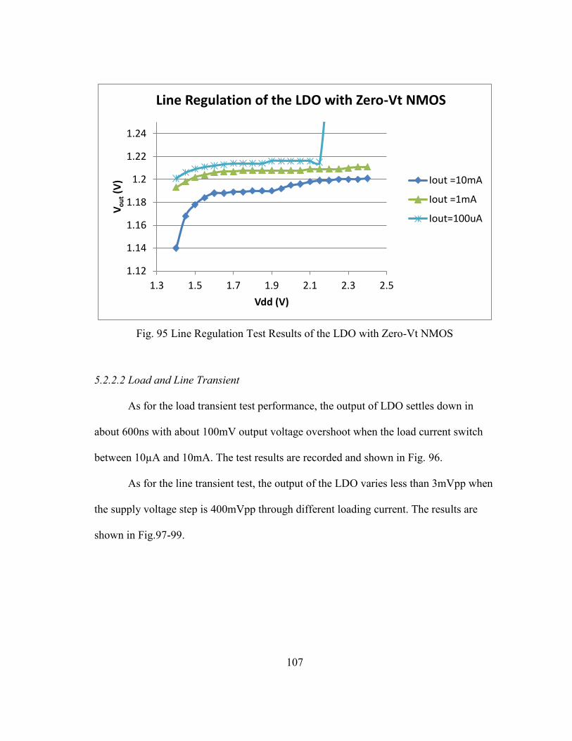
107
Fig. 95 Line Regulation Test Results of the LDO with Zero-Vt NMOS
5.2.2.2 Load and Line Transient
As for the load transient test performance, the output of LDO settles down in
about 600ns with about 100mV output voltage overshoot when the load current switch
between 10µA and 10mA. The test results are recorded and shown in Fig. 96.
As for the line transient test, the output of the LDO varies less than 3mVpp when
the supply voltage step is 400mVpp through different loading current. The results are
shown in Fig.97-99.
1.12
1.14
1.16
1.18
1.2
1.22
1.24
1.3 1.5 1.7 1.9 2.1 2.3 2.5
Vo
ut
(V)
Vdd (V)
Line Regulation of the LDO with Zero-Vt NMOS
Iout =10mA
Iout =1mA
Iout=100uA
108
VSW (2V/Div.)
0V
5V
Vout (20mV/Div.)
Time (200ns / Div.)
50ns
0V
5V
VSW (2V/Div.)
Vout (20mV/Div.)
50ns
Time (200ns / Div.)
(a) (b)
Fig. 96 Load Transient Test Results for 10µA to 10mA (a) and 10mA to 10µA (b)
Vdd (200mV / Div.)
Vout (2mV/Div.)
Time (20us / Div.)
2.4 mV
1.6 V
2.0 V
Fig. 97 Line Transient Test of the LDO with Zero-Vt for Iout = 10mA
109
Time (20us / Div.)
Vdd (200mV / Div.)
Vout (2mV/Div.)
2.5 mV
1.6 V
2.0 V
Fig. 98 Line Transient Test of the LDO with Zero-Vt for Iout = 1mA
Vdd (200mV / Div.)
1.6 V
2.0 V
2.1 mV
Time (20us / Div.)
Vout (2mV/Div.)
Fig. 99 Line Transient Test of the LDO with Zero-Vt for Iout = 100µA
110
5.2.2.3 PSR
The testing for the PSR measuring of the LDO with Zero-Vt is the same to that
used for the LDO with triple-well. Based on the testing data, the LDO is able to maintain
a PSR under −40dB for the frequency range up to 10MHz with the loading current from
100µA to 10mA. The LDO’s PSR test result is shown in Fig. 100.
Fig. 100 PSR Test Result of the LDO with Zero-Vt
5.3 Summary Table
A summary table of the measurement results of the two LDOs is put in Table 12.
The static and dynamic parameters of the two LDOs are compared. For the load transient
response part, the LDO with triple-well NMOS is of shorter settling time and smaller
overshoot voltage compared to the LDO with Zero-Vt NMOS. This is because the
-60
-50
-40
-30
-20
-10
0
1.0E+03 1.0E+04 1.0E+05 1.0E+06 1.0E+07 1.0E+08
PSR
(d
B)
Frequency (Hz)
PSR of the LDO with Zero-Vt NMOS
Iout =10mA
Iout =7mA
Iout =4mA
Iout =1mA
Iout =500uA
Iout =100uA
111
smaller pass transistor size when the triple-well NMOS is used. With smaller parasitic,
the LDO regulation loop is of larger bandwidth. This leads to the faster settling time and
smaller overshoot voltage. The LDO with triple-well NMOS pass transistor is also of
higher PSR bandwidth and lower current consumption. This is, again, due to the smaller
size of the triple-well NMOS pass transistor so that less current can be used to realize a
higher frequency pole at the gate of the pass transistor. However, the LDO with Zero-Vt
is of simpler structure without a charge pump. This leads to a quieter LDO output
voltage because the output ripple due the charge pump will be eliminated.
LDO with Triple-Well LDO with Zero-Vt
Vin / Vout 1.8V / 1.2V 1.8V / 1.2V
Max. Load Current 10mA 10mA
Line Regulation < 1mV / 100mV
(1.7V < Vdd < 2.1V)
< 1mV / 100mV
(1.6V < Vdd < 2.2V)
Load Regulation 4.3 mV/mA 2.2mV/mA
Load Transient
Settling Time
200ns 600ns
∆Vout in Load
Transient Response
44mV 100mV
Total Current
Consumption
265µA
350µA
CM Current
Consumption
165 µA 165 µA
Active Area 0.166mm2 0.183mm2
PSR −40dB to 19MHz 40dB to 10MHz
Table 12 Summary of the Test Results of the Proposed LDOs

112
5.4 Comparison with the State of Arts
Several LDO topologies are proposed to achieve good PSR in wide frequency
range and most good results are achieved for the LDOs with relatively smaller output
current. The two proposed LDOs are compared with the LDOs proposed in [10], [11]
and [17]. The maximum loading current for LDOs in [10], [11] and [17] are all no more
than 25mA. The design in [10], as discussed in Section 2.4.1, used cascode NMOS to
add more isolation from the power supply, but the internal compensation strategy limits
its high frequency PSR. The design in [11], as discussed in Section 2.4.2, using the feed-
forward technique to enhance the PSR of the LDO and achieved over -56dB PSR over
10MHz. However, the design uses an external capacitor to realize the external
compensation. This increases the BOM cost of using this design. The work in [17],
similar to the design in [12] discussed in Section 2.4.3, accommodating the feed-forward
technique into an internally compensated LDO design. It also introduces calibration
techniques to minimize the error of the feed-forward cancellation circuit but the PSR is
still limited to −22dB over 10MHz.
Compared with the design in [10], [11] and [17], the proposed LDO structure
achieves significant PSR over 10MHz while maintains a capacitor-less design.
Therefore, for the SoC design, accommodating the proposed LDO structure can help
reduce the pin number and save the BOM cost for the capacitor-less design. The wide
PSR bandwidth of the proposed LDO can help protect the noise sensitive circuits and

113
enable the usage of switching regulators with high working frequency. The detailed
comparison is shown in Table 13.
Parameter [10] in 2007 [11] in 2011 [18] in 2011 This Work
Technology 0.6µm 0.13µm 0.18µm 0.18µm
IMAX 5mA 25mA 25mA 10mA
Vin / Vout 1.8V / 1.2V 1.2V / 1.0V 1.8V / 1.5V 1.8V / 1.2V
IQ 70µA 50µA 300µA 265µA (Triple-Well)
350µA (Zero-Vt)
Active Area
(mm2)
N.A. 0.049 0.041 0.166 (Triple-Well)
0.183 (Zero-Vt)
Capacitor-Less
Design
Yes No Yes Yes
PSR -40dB @ 1MHz
-27dB @ 10MHz
-67dB @ 1MHz
-56dB @ 10MHz
-40dB @ 1MHz
-22dB @ 10MHz
-41dB @ 1MHz
-41dB @ 10MHz
Table 13 Comparison Table of the Proposed LDOs with the State of Arts Design
114
6. CONCLUSION
In this thesis, an externally compensated capacitor-less LDO structure is
proposed to achieve wide PSR bandwidth. To realize external compensation while
maintain the capacitor-less attribute, a new CM circuit is designed to implement a large
on-chip equivalent capacitance with limited on-chip capacitor. For the LDO design, both
triple-well NMOS and Zero-Vt NMOS are used as the pass transistor in LDO. The
triple-well pass transistor is of smaller size, so it can achieve a wider PSR bandwidth.
The Zero-Vt pass transistor is of negative threshold voltage but larger size. Therefore,
the LDO with Zero-Vt pass transistor does not need a charge pump for the pass transistor
gate driving, but it is of reduced PSR bandwidth.
A thorough analysis of the proposed LDO circuit and the CM circuit is provided
in the thesis. For the stability design, the limited working bandwidth of the CM makes it
working inductively at high frequency and introduces zeroes into the LDO’s regulation
loop. Similar situation happens to the parasitic loop of the CM, the poles inside the
LDO’s regulation loop also introduces zeroes into the CM’s loop. Therefore, the UGF of
the LDO’s regulation loop and the CM’s parasitic loop are extended by each other. This
leads to stability design issue. This problem is solved by inserting a shunting capacitor to
ground at the output of the LDO. This capacitor is added to cancel the high frequency
stability disturbance between the CM and the main LDO. For the PSR design, the CM
introduces extra paths from the supply to the LDO’s output if directly powered by the
supply voltage. These paths can degrade the LDO’s PSR at high frequency. Therefore,
115
the current sensing and the small signal amplifying part of the CM is supplied by the
LDO’s output instead of the power supply. With these design modifications, the CM
externally compensates the LDO without stability and PSR problems.
The proposed two LDO designs are fabricated in the IBM 0.18µm CMOS
technology. Through the experimental test, the two LDOs prove that they can supply
maximum 10mA current and achieves −40dB PSR over 10MHz. For the LDO with
triple-well pass transistor, static current consumption is 265µA and −40dB PSR up to
19MHz is achieved. For the LDO with Zero-Vt pass transistor, the static current
consumption is 350µA and −40dB PSR up to 10MHz is achieved. Compared with other
LDOs designed for high PSR over wide frequency range, the two proposed designs are
of significant PSR over 10MHz while maintain the capacitor-less attribute.
116
REFERENCES
[1] R.W. Erickson and D. Maksimovic, Fundamentals of Power Electronics, Norwell,
MA: Kluwer Academic, 2001.
[2] B. Manai, M. Bouguelaa and X. Rabeyrin, "A 0.65-0.9-1.2V supplies 10MHz high
efficiency PWM CMOS buck DC-DC converter," in Proc. IEEE International
Electronics, Circuits and Systems Conference, Dec. 2007, pp.1123-1126.
[3] S. Shapira, A. Unikovski, G. Peled, D.Cristea, E. Rotman, A. Eshkoli, A. Svetlitza
and Y. Nemirovsky, "CMOS DC to DC switched converter with on-chip inductors,"
in 2012 24th International Power Semiconductor Devices and ICs Symposium, June
2012, pp.69-72.
[4] D. Lu, J. Yu, Z. Hong, J. Mao and H. Zhao, "A 1500mA, 10MHz on-time controlled
buck converter with ripple compensation and efficiency optimization," in 2012
Twenty-Seventh Annual IEEE Applied Power Electronics Conference and
Exposition, Feb. 2012, pp.1232-1237.
[5] E. Z. Tabasy, A. Shafik, S. Huang, N.H.-W. Yang, S. Hoyos and S. Palermo, "A 6-
b 1.6-GS/s ADC with redundant cycle one-tap embedded DFE in 90-nm
CMOS," IEEE Journal of Solid-State Circuits, vol.48, no.8, pp.1885-1897, Aug.
2013.
[6] V. Dhanasekaran, M. Gambhir, M. M. Elsayed, E. Sanchez-Sinencio, J. Silva-
Martinez, C. Mishra, L. Chen and E. J. Pankratz, "A continuous time multi-
bit ∆Σ ADC using time domain quantizer and feedback element," IEEE Journal
of Solid-State Circuits , vol.46, no.3, pp.639-650, Mar. 2011.
[7] J. M. Ingino and V. R. von Kaenel, “A 4-GHz clock system for a high-performance
system-on-a-chip design," IEEE Journal of Solid-State Circuits, vol.36, no.11,
pp.1693-1698, Nov. 2001.
[8] V. R. von Kaenel, "A high-speed, low-power clock generator for a microprocessor
application," IEEE Journal of Solid-State Circuits, vol.33, no.11, pp.1634-1639,
Nov. 1998.
117
[9] B. Razavi, Design of Analog CMOS Integrated Circuits, Boston: McGraw-Hill
2001.
[10] E. Alon, J. Kim, S. Pamarti, K. Chang and M. Horowitz, "Replica compensated
linear regulators for supply-regulated phase-locked loops," IEEE Journal of Solid-
State Circuits, vol.41, no.2, pp.413-424, Feb. 2006.
[11] V. Gupta and G. A. Rincón-Mora, “A 5 mA 0.6µm CMOS Miller compensated
LDO regulator with -27 dB worst-case power-supply rejection using 60 pF of on-
chip capacitance,” in IEEE International Solid-State Circuits Conference Dig.
Tech. Papers, Feb. 2007, pp. 520-521.
[12] M. El-Nozahi, A. Amer, J. Torres, K. Entesari and E. Sanchez-Sinencio, "High PSR
low drop-out regulator with feed-forward ripple cancellation technique," IEEE
Journal of Solid-State Circuits, vol.45, no.3, pp.565-577, Mar. 2010.
[13] E.N.Y. Ho and P.K.T Mok, "Wide-loading-range fully integrated LDR with a
power-supply ripple injection filter," IEEE Transactions on Circuits and Systems
II: Express Briefs, vol.59, no.6, pp.356-360, June 2012.
[14] V. Gupta, G.A. Rincon-Mora and P. Raha, "Analysis and design of monolithic, high
PSR, linear regulators for SoC applications," in Proc. IEEE International SoC
Conference, Sept. 2004, pp.311-315.
[15] G. Palumbo and D. Pappalardo, "Charge pump circuits: an overview on design
strategies and topologies," IEEE Circuits and Systems Magazine, vol.10, no.1,
pp.31-45, First Quarter 2010.
[16] K.-J. Baek, J.-M. Gim, H.-S. Kim, K.-Y. Na, N.-S. Kim and Y.-S. Kim, "Analogue
circuit design methodology using self-cascode structures," Electronics Letters ,
vol.49, no.9, pp.591-592, Apr. 2013
[17] J. Silva-Martinez and A. Vazquez-Gonzalez "Impedance scalers for IC active
filters," in Proc. IEEE International Symposium on Circuits and Systems, June
1998, vol.1, pp.151-154.

118
[18] B. Yang, B. Drost, S. Rao and P. K. Hanumolu, "A high-PSR LDO using a
feedforward supply-noise cancellation technique," in Proc. 2011 IEEE Custom
Integrated Circuits Conference, Sept. 2011, pp.1-4.