Embed Size (px)
Citation preview
A 6Gbps Transmitter with
ISI and Reflection Cancellation
by
Ricky Yuen
A thesis submitted in conformity with the requirements
for the degree of Master of Applied ScienceGraduate Department of Electrical and Computer Engineering
University of Toronto
c© Copyright by Ricky Yuen 2005

A 6Gbps Transmitter with
ISI and Reflection Cancellation
Ricky Yuen
Master of Applied Science, 2005
Graduate Department of Electrical and Computer Engineering
University of Toronto
Abstract
This thesis presents the design and implementation of a high-speed chip-to-chip transmit-
ter with Intersymbol Interference (ISI)-cancellation circuitry and reflection-cancellation
circuitry. The transmitter has a 2-way interleaving architecture with an aggregate data
rate of 6Gbps. To cancel ISI, the transmitter uses a 3-tap pre-emphasis driver. As for the
reflection-cancellation circuitry, the transmitter uses an 8-tap reflection canceller with
one Unit Interval (UI) resolution. The 8 continuous taps can be delayed from 0 to 126
unit intervals to match the timing of the reflections. A testchip of the transmitter is de-
signed in Fujitsu’s 0.11µm CMOS technology to demonstrate our reflection-cancellation
technique. The testchip includes a 3GHz Phase Locked Loop (PLL) to serve as a clock
generator for the transmitter testchip.
ii

Acknowledgements
I would like to say thank you to my professor, Ali Sheikholeslami, for his support and
guidance in my thesis. Without his recommendation to Fujitsu, this project would not
have been possible. His comments and encouragments always lead me down the right
direction and take me one step closer to a successful project.
Also, many thanks to William Walker, director of Fujitsu Laboratories of America,
for his patience and guidance during my three months stay in Sunnyvale. The work
experience and knowledge I gained from working there is invaluable. I would like to
thank my co-workers in Fujitsu for their countless support.
Special thank you to Hirotaka Tamura-san for his initial idea on the project. His
experience in the field helped me significantly in planning the transmitter architecture.
Thank you to all students in BA5000 for their help and friendship they have given me
in the last two years.
Finally, I would like to say thank you to my parents, Stephen and Maggie. They have
always encouraged me and provided tremendous daily support during my busiest days.
I would also like to thank my brother, Ken, for all the fun we had together.
iii

Contents
List of Figures vi
List of Tables ix
1 Introduction 1
1.1 Motivation . . . . . . . . . . . . . . . . . . . . . . . . . . . . . . . . . . . 11.2 Objective . . . . . . . . . . . . . . . . . . . . . . . . . . . . . . . . . . . 21.3 Organization of the Thesis . . . . . . . . . . . . . . . . . . . . . . . . . . 2
2 Background: High-Speed Signaling 4
2.1 Lossy Transmission Line and Intersymbol Interference . . . . . . . . . . . 42.2 Equalization Techniques . . . . . . . . . . . . . . . . . . . . . . . . . . . 6
2.2.1 Pre-Emphasis Equalization . . . . . . . . . . . . . . . . . . . . . . 62.2.2 Post-Equalization . . . . . . . . . . . . . . . . . . . . . . . . . . . 9
2.3 Reflections . . . . . . . . . . . . . . . . . . . . . . . . . . . . . . . . . . . 122.3.1 Resistive Reflection . . . . . . . . . . . . . . . . . . . . . . . . . . 132.3.2 Capacitive Reflection . . . . . . . . . . . . . . . . . . . . . . . . . 152.3.3 Inductive Reflection . . . . . . . . . . . . . . . . . . . . . . . . . . 16
2.4 Reflection Cancellation . . . . . . . . . . . . . . . . . . . . . . . . . . . . 182.5 System Simulation . . . . . . . . . . . . . . . . . . . . . . . . . . . . . . 182.6 Summary . . . . . . . . . . . . . . . . . . . . . . . . . . . . . . . . . . . 20
3 Transmitter Design 22
3.1 Approach to Reflection-Cancellation . . . . . . . . . . . . . . . . . . . . . 223.2 Top Level Description . . . . . . . . . . . . . . . . . . . . . . . . . . . . 243.3 Transmitter Digital Block . . . . . . . . . . . . . . . . . . . . . . . . . . 25
3.3.1 Data Generator . . . . . . . . . . . . . . . . . . . . . . . . . . . . 273.3.2 Variable Delay Block . . . . . . . . . . . . . . . . . . . . . . . . . 293.3.3 Dummy Delay Block . . . . . . . . . . . . . . . . . . . . . . . . . 303.3.4 Negative Alignment Block . . . . . . . . . . . . . . . . . . . . . . 313.3.5 Bit Inversion Block . . . . . . . . . . . . . . . . . . . . . . . . . . 323.3.6 The Scan Mechanism and the Mini-JTAG Controller . . . . . . . 333.3.7 Scan-Chain . . . . . . . . . . . . . . . . . . . . . . . . . . . . . . 353.3.8 Transmitter Control Block . . . . . . . . . . . . . . . . . . . . . . 36
iv

Contents
3.3.9 Transmitter Digital Block Layout . . . . . . . . . . . . . . . . . . 373.4 The Transmitter Front-End Block . . . . . . . . . . . . . . . . . . . . . . 39
3.4.1 High-Speed Data Multiplexor . . . . . . . . . . . . . . . . . . . . 393.4.2 Bias Circuit . . . . . . . . . . . . . . . . . . . . . . . . . . . . . . 413.4.3 Driver Circuits . . . . . . . . . . . . . . . . . . . . . . . . . . . . 423.4.4 Transmitter Front-End Layout . . . . . . . . . . . . . . . . . . . . 47
3.5 Phase Locked Loop . . . . . . . . . . . . . . . . . . . . . . . . . . . . . . 473.5.1 PLL Layout . . . . . . . . . . . . . . . . . . . . . . . . . . . . . . 52
3.6 Primitive Circuits . . . . . . . . . . . . . . . . . . . . . . . . . . . . . . . 523.6.1 Sense-Amplifier Flip-Flop . . . . . . . . . . . . . . . . . . . . . . 533.6.2 Sense-Amplifier Multiplexor Flip-Flop . . . . . . . . . . . . . . . 553.6.3 High-speed Digital 2-to-1 Multiplexor . . . . . . . . . . . . . . . . 56
3.7 Summary . . . . . . . . . . . . . . . . . . . . . . . . . . . . . . . . . . . 56
4 System Operation Modes and Simulation Results 58
4.1 System Operation Modes . . . . . . . . . . . . . . . . . . . . . . . . . . . 584.1.1 Scan-in Mode . . . . . . . . . . . . . . . . . . . . . . . . . . . . . 584.1.2 Calibration Mode . . . . . . . . . . . . . . . . . . . . . . . . . . . 594.1.3 Data Transmission Mode . . . . . . . . . . . . . . . . . . . . . . . 60
4.2 Simulation Results . . . . . . . . . . . . . . . . . . . . . . . . . . . . . . 604.2.1 Reflection Cancellation . . . . . . . . . . . . . . . . . . . . . . . . 604.2.2 ISI Cancellation . . . . . . . . . . . . . . . . . . . . . . . . . . . . 654.2.3 Power Consumption . . . . . . . . . . . . . . . . . . . . . . . . . 68
4.3 PLL Simulation . . . . . . . . . . . . . . . . . . . . . . . . . . . . . . . . 704.3.1 PLL Lock Acquistion . . . . . . . . . . . . . . . . . . . . . . . . . 704.3.2 Phase Noise . . . . . . . . . . . . . . . . . . . . . . . . . . . . . . 71
4.4 Transmitter Testchip Layout and Specifications . . . . . . . . . . . . . . 724.5 Summary . . . . . . . . . . . . . . . . . . . . . . . . . . . . . . . . . . . 73
5 Conclusions 75
5.1 Summary . . . . . . . . . . . . . . . . . . . . . . . . . . . . . . . . . . . 755.2 Contributions . . . . . . . . . . . . . . . . . . . . . . . . . . . . . . . . . 765.3 Future Work . . . . . . . . . . . . . . . . . . . . . . . . . . . . . . . . . . 76
References 78
v

List of Figures
2.1 Simplified chip-to-chip signaling system. . . . . . . . . . . . . . . . . . . 42.2 Channel frequency response of a 50cm PCB trace. . . . . . . . . . . . . . 52.3 Cross sectional view of a PCB W-element model. . . . . . . . . . . . . . 62.4 ISI in a 50cm PCB trace. (a) Channel input transient response. (b)
Channel output transient response. . . . . . . . . . . . . . . . . . . . . . 72.5 Data transmission affected by ISI. (a) Transmitted signal. (b) Received
signal. . . . . . . . . . . . . . . . . . . . . . . . . . . . . . . . . . . . . . 82.6 The idea behind pre-emphasis equalization. . . . . . . . . . . . . . . . . . 82.7 Data transmission with pre-emphasis. (a) Transmitted signal. (b) Re-
ceived signal. . . . . . . . . . . . . . . . . . . . . . . . . . . . . . . . . . 92.8 Pre-emphasis circuit implementation. . . . . . . . . . . . . . . . . . . . . 92.9 The generation of the pre-emphasis waveform. (a) Signal from data driver.
(b) Signal from pre-emphasis driver. (c) Signal at the output node. . . . 102.10 The transmitter implemented by Lin [LWJ03]. . . . . . . . . . . . . . . . 102.11 The idea behind post-equalization. . . . . . . . . . . . . . . . . . . . . . 112.12 The idea behind feed-forward equalizer. . . . . . . . . . . . . . . . . . . . 112.13 DFE block diagram. . . . . . . . . . . . . . . . . . . . . . . . . . . . . . 122.14 The DFE ISI correction process. (a) The received signal. (b) The feedback
signal. (c) The ISI-free signal ready for detection. . . . . . . . . . . . . . 122.15 Resistive reflection from termination mismatches. . . . . . . . . . . . . . 132.16 Lattice diagram showing multiple resistive reflections. . . . . . . . . . . . 142.17 Capacitive reflection from connectors. . . . . . . . . . . . . . . . . . . . . 152.18 Simulation of capacitive reflection along the channel. . . . . . . . . . . . 162.19 Inductive reflection along the channel. . . . . . . . . . . . . . . . . . . . 172.20 Simulation of inductive reflection along the channel. . . . . . . . . . . . . 172.21 The 1m PCB channel used to determine the number of ISI taps needed. . 182.22 The impulse response of a 1m PCB channel. . . . . . . . . . . . . . . . . 192.23 The PCB channel used to determine the number of reflection taps needed. 192.24 The impulse response of a 8cm PCB channel with connectors. . . . . . . 20
3.1 System overview. . . . . . . . . . . . . . . . . . . . . . . . . . . . . . . . 233.2 Approach to reflection cancellation. (a) Transmitter output. (b) Receiver
input. . . . . . . . . . . . . . . . . . . . . . . . . . . . . . . . . . . . . . 233.3 Top level block diagram. . . . . . . . . . . . . . . . . . . . . . . . . . . . 25
vi
List of Figures
3.4 The transmitter digital block. . . . . . . . . . . . . . . . . . . . . . . . . 263.5 The transmitter data generator. . . . . . . . . . . . . . . . . . . . . . . . 283.6 Variable delay block implemented with only 2-to-1 multiplexors and flip-
flops. (a) Implementation with constant delay but large input loading.(b) Implementation with long zero-delay path but small input loading. . 30
3.7 The timing diagram of the signals in the variable delay block. . . . . . . 313.8 The dummy delay block. . . . . . . . . . . . . . . . . . . . . . . . . . . . 313.9 The negative alignment block. . . . . . . . . . . . . . . . . . . . . . . . . 323.10 The negative alignment block timing diagram. . . . . . . . . . . . . . . . 323.11 The bit inversion block. . . . . . . . . . . . . . . . . . . . . . . . . . . . 333.12 Overview of the scan mechanism in the transmitter. . . . . . . . . . . . . 343.13 The mini-JTAG controller FSM. . . . . . . . . . . . . . . . . . . . . . . . 353.14 The transmitter scan-chain. . . . . . . . . . . . . . . . . . . . . . . . . . 363.15 The transmitter control block. . . . . . . . . . . . . . . . . . . . . . . . . 373.16 Transmitter digital block layout. . . . . . . . . . . . . . . . . . . . . . . . 383.17 The transmitter front-end block. . . . . . . . . . . . . . . . . . . . . . . . 403.18 The 6Gbps high-speed data multiplexor. . . . . . . . . . . . . . . . . . . 413.19 Timing diagram of the high-speed data multiplexor. . . . . . . . . . . . . 423.20 The wide-swing cascode bias circuit for data driver. . . . . . . . . . . . . 423.21 The data driver. . . . . . . . . . . . . . . . . . . . . . . . . . . . . . . . . 433.22 The 4-bit controlled variable termination resistor. . . . . . . . . . . . . . 433.23 The current source for the data driver. . . . . . . . . . . . . . . . . . . . 443.24 The 3-tap pre-emphasis driver. . . . . . . . . . . . . . . . . . . . . . . . . 453.25 The 8-tap reflection-cancellation driver. . . . . . . . . . . . . . . . . . . . 463.26 The current source for the pre-emphasis drivers and reflection canceller. . 473.27 Transmitter front-end layout. . . . . . . . . . . . . . . . . . . . . . . . . 483.28 Top level PLL diagram. . . . . . . . . . . . . . . . . . . . . . . . . . . . 483.29 Relationship between charge pump current and phase difference between
ref clk and fb clk. . . . . . . . . . . . . . . . . . . . . . . . . . . . . . . 493.30 LC-VCO Block. . . . . . . . . . . . . . . . . . . . . . . . . . . . . . . . . 503.31 VCO tuning range. . . . . . . . . . . . . . . . . . . . . . . . . . . . . . . 503.32 The schematic of the clock divider. . . . . . . . . . . . . . . . . . . . . . 513.33 The schematic of the asynchronous enable block. . . . . . . . . . . . . . . 513.34 The asynchronous enable block circuit timing diagram. . . . . . . . . . . 523.35 3GHz PLL layout. . . . . . . . . . . . . . . . . . . . . . . . . . . . . . . 533.36 The sense-amplifier flip-flop. . . . . . . . . . . . . . . . . . . . . . . . . . 543.37 The combined 2-to-1 multiplexor and sense-amplifier flip-flop. . . . . . . 553.38 The high-speed 2-to-1 multiplexor. . . . . . . . . . . . . . . . . . . . . . 56
4.1 Scan-in operation. . . . . . . . . . . . . . . . . . . . . . . . . . . . . . . . 594.2 Channel with termination mismatches used in reflection cancellation sim-
ulation. . . . . . . . . . . . . . . . . . . . . . . . . . . . . . . . . . . . . 61
vii
List of Figures
4.3 The channel impulse response before and after reflection cancellation. . . 624.4 Received signal eye diagram before reflection cancellation. . . . . . . . . 634.5 Received signal eye diagram after reflection cancellation. . . . . . . . . . 634.6 Channel with impedance discontinuities used in reflection cancellation
simulation. . . . . . . . . . . . . . . . . . . . . . . . . . . . . . . . . . . . 644.7 The channel impulse response before and after reflection cancellation. . . 654.8 Received signal eye diagram before reflection cancellation. . . . . . . . . 664.9 Received signal eye diagram after reflection cancellation. . . . . . . . . . 664.10 Channel model used in ISI cancellation simulation. . . . . . . . . . . . . 674.11 The channel impulse response before and after ISI cancellation. . . . . . 684.12 Received signal eye diagram before ISI cancellation. . . . . . . . . . . . . 694.13 Received signal eye diagram after ISI cancellation. . . . . . . . . . . . . . 694.14 Contributions of the transmitter power consumption. . . . . . . . . . . . 704.15 PLL lock acquisition. . . . . . . . . . . . . . . . . . . . . . . . . . . . . . 714.16 PLL phase noise plot. . . . . . . . . . . . . . . . . . . . . . . . . . . . . . 724.17 Testchip layout. . . . . . . . . . . . . . . . . . . . . . . . . . . . . . . . . 73
viii

List of Tables
3.1 Data generator functions. . . . . . . . . . . . . . . . . . . . . . . . . . . 283.2 PRBS sequence example. . . . . . . . . . . . . . . . . . . . . . . . . . . . 283.3 JTAG pin list. . . . . . . . . . . . . . . . . . . . . . . . . . . . . . . . . . 343.4 FSM states representation and output. . . . . . . . . . . . . . . . . . . . 353.5 Detailed scan-chain bit representation. . . . . . . . . . . . . . . . . . . . 373.6 Transmitter control logic truth table. . . . . . . . . . . . . . . . . . . . . 383.7 Truth table for data multiplexor invpos and invneg pins. . . . . . . . . . 41
4.1 Transmitter testchip specifications. . . . . . . . . . . . . . . . . . . . . . 74
ix

List of Acronyms
BER Bit Error Rate
BERT Bit Error Rate Tester
CMOS Complementary Metal Oxide Silicon
dB Decibel
DFE Decision Feedback Equalizer
FLA Fujitsu Laboratories of America
FSM Finite State Machine
GHz Giga Hertz
LC Inductor and Capacitor
IEEE Institute of Electrical and Electronics Engineers
IC Integrated Circuit
ISI Intersymbol Interference
JTAG Joint Test Action Group
LSB Least Significant Bit
MHz Mega Hertz
MOSFET Metal Oxide Semiconductor Field Effect Transistor
MSB Most Significant Bit
NMOS Negative-Channel Metal Oxide Semiconductor
PCB Printed Circuit Board
PRBS Pseudo Random Bit Sequence
PMOS Positive-Channel Metal Oxide Semiconductor
x

List of Acronyms
PLL Phase Locked Loop
RMS Root Mean Square
UI Unit Interval
VCO Voltage Controlled Oscillator
xi
1 Introduction
1.1 Motivation
The need to quickly transfer large amount of data between chips on Printed Circuit
Boards (PCBs) has accelerated the research of high-speed signaling. New circuit tech-
niques have been developed to allow faster data transmission [FMWK97], to have more
accurate data recovery [SR01], and to obtain better signal quality [FMWK97] [Son96]
[KFM02]. With these circuit techniques, transceivers are able to transmit several giga-
bits of data per second per pin over PCB traces [FMWK97] [TTM+03].
The increase in signaling speed over PCB traces introduces transmission line effects
on the signal. Examples of transmission line effects include skin effect and reflection.
Skin effect of a conductor, such as a PCB trace, causes high frequency components of
the travelling signal to concentrate at the periphery of the conductor and leads to an
increase in its resistance. Skin effect is the dominant cause of the frequency-dependent
attenuation of PCB traces [HHM00], and manifests itself as intersymbol interference
(ISI). ISI causes the energy of a single bit to spread to adjacent bits causing interference.
Reflections occur when signals experience impedance mismatches along the channel.
These reflections, if they travel back to the receiver, interfere with the received signal.
Signal interference caused by ISI and reflection leads to higher bit error rate (BER) and
limits data transmission speed.
Channels in backplane systems could have many impedance mismatches that cause
reflections. A backplane is a type of system that has multiple line cards communicating
over a common channel. The chips on the line cards are connected in a bus topology
through the use of connectors, vias, and PCB traces [HHM00]. In addition, the chips
are usually packaged before they are soldered on the line cards. Thus, the channel for
chip-to-chip signaling on the backplane includes not only the PCB trace that causes ISI,
but also the connectors, vias, and chip packagings that cause reflections.
Reflections and ISI affect the received signal on backplanes and lead to detection er-
1

1 Introduction
rors. The transceiver developed by Zerbe et al. [ZWS+03] uses a pre-emphasis scheme
to equalize ISI and a Decision Feedback Equalizer (DFE) to cancel reflections. Pre-
emphasis is a method implemented in the transmitter to equalize ISI by amplifying the
high frequency components of the transmitted signal, in anticipation of the frequency
dependent loss of the channel. DFE is a method implemented in the receiver to com-
pensate for the loss of the received signal prior to signal detection. However, a DFE
has a more complicated implementation compared to pre-emphasis. This is because a
DFE deals with both the analog received signal and the digital recovered signal while a
pre-emphasis driver only deals with the digital data bits.
By extending the idea of pre-emphasis, we propose implementing the reflection cancel-
lation at the transmitter. Instead of canceling reflections at the receiver, the transmitter
is programmed to send out reflection-cancellation signals such that the sum of the re-
flection signal and the cancellation signal is zero. The benefits of cancelling reflections
at the transmitter are increased effectiveness, accuracy, and ease of implementation. By
canceling the reflections before they travel back to the receiver, this technique eliminates
the occurrences of multiple reflections that further interfere with the received signal.
1.2 Objective
The objective of this research is to develop a transmitter with reflection cancellation
and ISI cancellation capability for high-speed chip-to-chip signaling. A 3GHz PLL is to
be designed as the clock generator for the transmitter. The transmitter has a targeted
data rate of 6Gbps. A testchip of the transmitter will be implemented with Fujitsu
Laboratories of America (FLA) 0.11µm CMOS process.
1.3 Organization of the Thesis
The subsequent chapters of the thesis are organized as follows. Chapter 2 covers the
background material on high-speed signaling, including ISI for long and lossy channels as
well as signal reflections due to impedance mismatches. Chapter 2 also discusses previous
approaches for compensating ISI. Chapter 3 presents our approach to equalizing the
signal reflection at the transmitter. This chapter also provides details of the transmitter
circuits including the transmitter digital block, the transmitter front-end, and a 3GHz
2

1 Introduction
PLL designed as a clock generator for the transmitter. Chapter 4 shows the simulation
results for both the transmitter and the PLL. Simulations include received signal eye
diagrams showing the improvments in the eye opening, with the reflection-cancellation
drivers enabled. Finally, chapter 5 concludes the thesis by summarizing the contributions
of this research.
3
2 Background: High-Speed Signaling
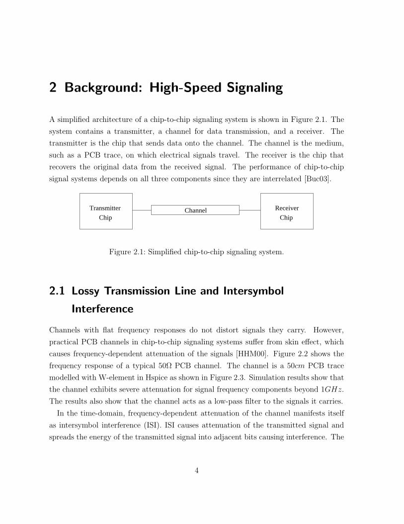
A simplified architecture of a chip-to-chip signaling system is shown in Figure 2.1. The
system contains a transmitter, a channel for data transmission, and a receiver. The
transmitter is the chip that sends data onto the channel. The channel is the medium,
such as a PCB trace, on which electrical signals travel. The receiver is the chip that
recovers the original data from the received signal. The performance of chip-to-chip
signal systems depends on all three components since they are interrelated [Buc03].
ChipChannel
Chip
Transmitter Receiver
Figure 2.1: Simplified chip-to-chip signaling system.
2.1 Lossy Transmission Line and Intersymbol
Interference
Channels with flat frequency responses do not distort signals they carry. However,
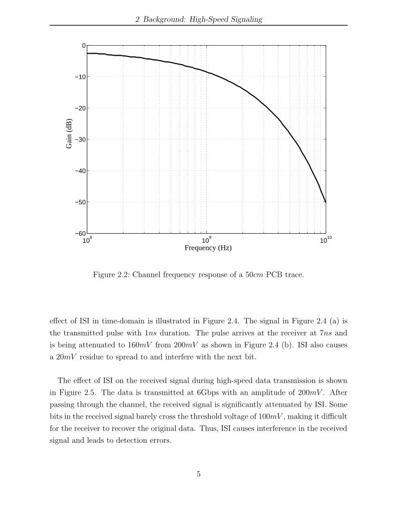
practical PCB channels in chip-to-chip signaling systems suffer from skin effect, which
causes frequency-dependent attenuation of the signals [HHM00]. Figure 2.2 shows the
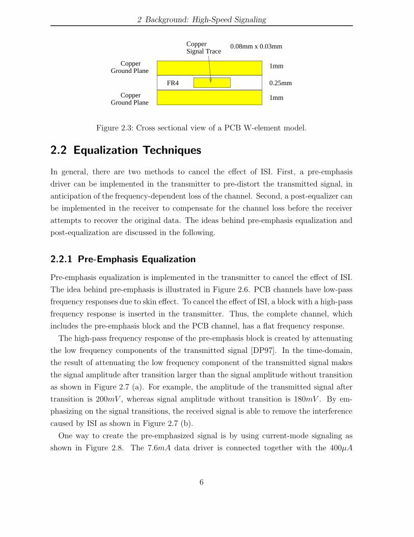
frequency response of a typical 50Ω PCB channel. The channel is a 50cm PCB trace
modelled with W-element in Hspice as shown in Figure 2.3. Simulation results show that
the channel exhibits severe attenuation for signal frequency components beyond 1GHz.
The results also show that the channel acts as a low-pass filter to the signals it carries.
In the time-domain, frequency-dependent attenuation of the channel manifests itself
as intersymbol interference (ISI). ISI causes attenuation of the transmitted signal and
spreads the energy of the transmitted signal into adjacent bits causing interference. The
4
2 Background: High-Speed Signaling
108
109
1010
−60
−50
−40
−30
−20
−10
0
Frequency (Hz)
Gai
n (d
B)
Figure 2.2: Channel frequency response of a 50cm PCB trace.
effect of ISI in time-domain is illustrated in Figure 2.4. The signal in Figure 2.4 (a) is
the transmitted pulse with 1ns duration. The pulse arrives at the receiver at 7ns and
is being attenuated to 160mV from 200mV as shown in Figure 2.4 (b). ISI also causes
a 20mV residue to spread to and interfere with the next bit.
The effect of ISI on the received signal during high-speed data transmission is shown
in Figure 2.5. The data is transmitted at 6Gbps with an amplitude of 200mV . After
passing through the channel, the received signal is significantly attenuated by ISI. Some
bits in the received signal barely cross the threshold voltage of 100mV , making it difficult
for the receiver to recover the original data. Thus, ISI causes interference in the received
signal and leads to detection errors.
5
2 Background: High-Speed Signaling
0.08mm x 0.03mm
CopperGround Plane
1mm
1mm
0.25mmFR4
Ground PlaneCopper
CopperSignal Trace
Figure 2.3: Cross sectional view of a PCB W-element model.
2.2 Equalization Techniques
In general, there are two methods to cancel the effect of ISI. First, a pre-emphasis
driver can be implemented in the transmitter to pre-distort the transmitted signal, in
anticipation of the frequency-dependent loss of the channel. Second, a post-equalizer can
be implemented in the receiver to compensate for the channel loss before the receiver
attempts to recover the original data. The ideas behind pre-emphasis equalization and
post-equalization are discussed in the following.
2.2.1 Pre-Emphasis Equalization
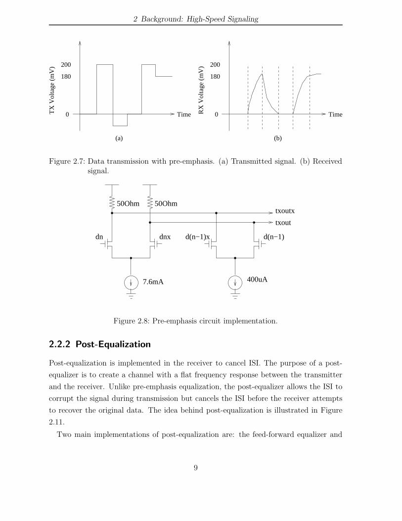
Pre-emphasis equalization is implemented in the transmitter to cancel the effect of ISI.
The idea behind pre-emphasis is illustrated in Figure 2.6. PCB channels have low-pass
frequency responses due to skin effect. To cancel the effect of ISI, a block with a high-pass
frequency response is inserted in the transmitter. Thus, the complete channel, which
includes the pre-emphasis block and the PCB channel, has a flat frequency response.
The high-pass frequency response of the pre-emphasis block is created by attenuating
the low frequency components of the transmitted signal [DP97]. In the time-domain,
the result of attenuating the low frequency component of the transmitted signal makes
the signal amplitude after transition larger than the signal amplitude without transition
as shown in Figure 2.7 (a). For example, the amplitude of the transmitted signal after
transition is 200mV , whereas signal amplitude without transition is 180mV . By em-
phasizing on the signal transitions, the received signal is able to remove the interference
caused by ISI as shown in Figure 2.7 (b).
One way to create the pre-emphasized signal is by using current-mode signaling as
shown in Figure 2.8. The 7.6mA data driver is connected together with the 400µA
6

2 Background: High-Speed Signaling
0 2 4 6 8 10 12 14 16 18 20−50
0
50
100
150
200
250
Time (ns)
TX
Vol
tage
(m
V)
0 2 4 6 8 10 12 14 16 18 200
50
100
150
200
Time (ns)
RX
Vol
tage
(m
V)
(a)
(b)
Figure 2.4: ISI in a 50cm PCB trace. (a) Channel input transient response. (b) Channeloutput transient response.
pre-emphasis driver at the output nodes, txout and txoutx. dn and dnx are data inputs,
and d(n − 1) and d(n − 1)x are data inputs delayed by one UI.
To illustrate how the pre-emphasis driver functions, the transmitted data is assumed
to be equal to dn = [-1, 1, -1, -1]. The data driver produces 190mV of output swing
and the pre-emphasis driver produces 10mV of output swing as shown in Figure 2.9.
The polarity of the 1UI delayed data to the pre-emphasis driver is flipped to emphasize
the signal transitions. The output of the pre-emphasis driver is the inverted and 1UI
delayed version of the output of the data driver. The pre-emphasized signal is created
by current summing the output of the data driver and the pre-emphasis driver.
Recently, a 5Gbps transmitter with pre-emphasis is designed by Lin as shown in Figure
2.10 [LWJ03]. The main driver has 10.5mA of current which produces 250mV output
swing. There are two pre-emphasis drivers: Tap1 uses the 1UI delayed data and Tap2
7

2 Background: High-Speed Signaling
0 500 1000 1500 2000 2500 3000 3500 4000 4500−50
0
50
100
150
200
Time (ps)
Vol
tage
(m
V)
0 500 1000 1500 2000 2500 3000 3500 4000 45000
50
100
150
200
Time (ps)
Vol
tage
(m
V)
(a)
(b)
Figure 2.5: Data transmission affected by ISI. (a) Transmitted signal. (b) Receivedsignal.
f f
Data Driver
Transmitter
Pre−emphasis Channel Receiver
0100110
Figure 2.6: The idea behind pre-emphasis equalization.
uses the 2UI delayed data. The current in Tap1 is controlled by a 7-bit digital input
and the current in Tap2 is controlled by a 3-bit digital input. With this architecture,
the transmitter is able to transmit data at 5Gbps over a 15m coaxial cable.
8
2 Background: High-Speed Signaling
(b)
0
180
200
TimeRX
Vol
tage
(m
V)200
TimeTX
Vol
tage
(m
V)
(a)
0
180
Figure 2.7: Data transmission with pre-emphasis. (a) Transmitted signal. (b) Receivedsignal.
txoutx
txout
400uA7.6mA
50Ohm 50Ohm
d(n−1)dn dnx d(n−1)x
Figure 2.8: Pre-emphasis circuit implementation.
2.2.2 Post-Equalization
Post-equalization is implemented in the receiver to cancel ISI. The purpose of a post-
equalizer is to create a channel with a flat frequency response between the transmitter
and the receiver. Unlike pre-emphasis equalization, the post-equalizer allows the ISI to
corrupt the signal during transmission but cancels the ISI before the receiver attempts
to recover the original data. The idea behind post-equalization is illustrated in Figure
2.11.
Two main implementations of post-equalization are: the feed-forward equalizer and
9

2 Background: High-Speed Signaling
(c)
Time
Time
−180−200
200
−10
10
−190
190
(a)
(b)
Time
1 −1−1 −1
Out
put (
mV
)Pr
e−em
ph D
rive
r (m
V)
Dat
a D
rive
r (m
V)
Figure 2.9: The generation of the pre-emphasis waveform. (a) Signal from data driver.(b) Signal from pre-emphasis driver. (c) Signal at the output node.
50Ohm
MainDriver
Tap2Tap1
10.5mA 15.2mA 4mA
out
outb
50Ohm
Figure 2.10: The transmitter implemented by Lin [LWJ03].
10

2 Background: High-Speed Signaling
f
Transmitter Channel Decision circuit
Receiver
Post Equalizer
f
0100110
Figure 2.11: The idea behind post-equalization.
the Decision Feedback Equalizer (DFE). The feed-forward equalizer samples the received
signal, and subtracts from it a fraction of the previous sample. The amount of subtrac-
tion depends on the ISI in the current sample. Figure 2.12 shows the block diagram
of a feed-forward equalizer where the depth of ISI is one. This means ISI only cause
interference to one adjacent bit. Extra feed forward paths are required to cancel ISI
with depth higher than one.
a
−
To Decision Circuit
1UI
Received Data
Figure 2.12: The idea behind feed-forward equalizer.
The idea behind a DFE is similar to a feed-forward equalizer. Instead of subtracting
a fraction of the previous sample from the current sample of the received signal, a DFE
subtracts a scaled version of the recovered data from the current sample of the received
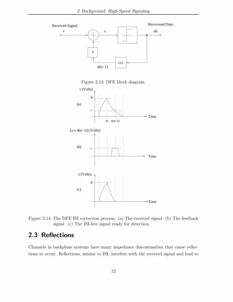
signal. Figure 2.13 shows the block diagram of a DFE where the depth of ISI is one. The
received signal r is subtracted by a correction signal given by a×d(n−1), where d(n−1)
is the previous recovered data and a is the scale factor. The result of the subtraction s,
the ISI-free received signal, enters the decision circuit to recover the original data.
Figure 2.14 illustrates the ISI subtraction in the DFE. The received signal r shown in
Figure 2.14 (a) has ISI equal to c. To cancel the ISI, it is necessary to subtract c from
the received signal at time t(n + 1). The correction signal is the scaled version of the
recovered data as shown in Figure 2.14 (b). The correction signal is subtracted from the
received signal r to become the ISI-free signal s as shown in Figure 2.14 (c).
11
2 Background: High-Speed Signaling
d(n−1)1UI
a
dnr
Received Signal Recovered Data
s
−
Figure 2.13: DFE block diagram.
Time
R
(a)
c(b)
R
(c)
tn t(n+1)
c
s (Volts)
Time
r (Volts)
Time
[a x d(n−1)] (Volts)
Figure 2.14: The DFE ISI correction process. (a) The received signal. (b) The feedbacksignal. (c) The ISI-free signal ready for detection.
2.3 Reflections
Channels in backplane systems have many impedance discontinuities that cause reflec-
tions to occur. Reflections, similar to ISI, interfere with the received signal and lead to
12
2 Background: High-Speed Signaling
detection errors. Practically, reflections are unavoidable since any impedance mismatch
along the channel lead to reflections. Examples of impedance mismatches in backplane
systems include PCB vias, connectors, bondwires, and termination resistors.
Reflections can be classified into three main types: resistive, capacitive, and inductive
[HHM00]. Resistive reflection is the simplest to understand as the reflection is only
an attenutated version of the original signal. Examples of impedance mismatches that
cause resistive reflections include PCB vias and termination resistors. Capacitors and
inductors are time-dependent elements and generate reflections that look different from
the original signal. Connectors, for example, cause capacitive reflections while bondwires
and PCB vias cause inductive reflections in backplane systems.
2.3.1 Resistive Reflection
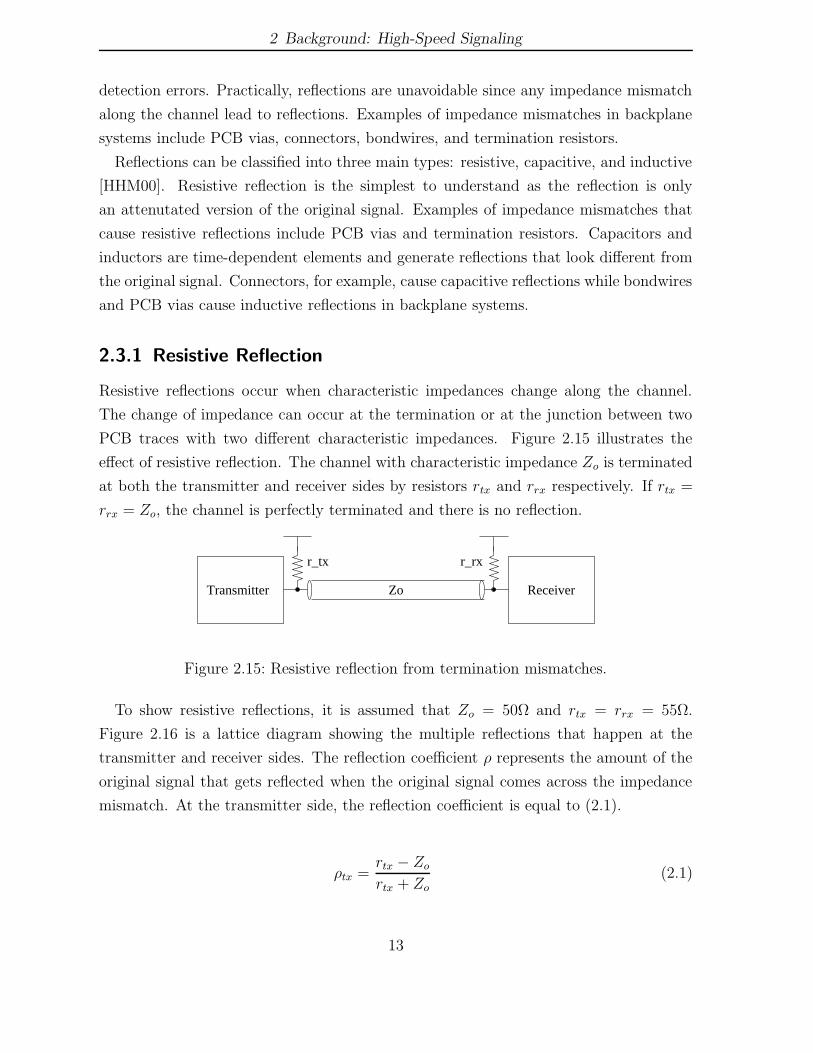
Resistive reflections occur when characteristic impedances change along the channel.
The change of impedance can occur at the termination or at the junction between two
PCB traces with two different characteristic impedances. Figure 2.15 illustrates the
effect of resistive reflection. The channel with characteristic impedance Zo is terminated
at both the transmitter and receiver sides by resistors rtx and rrx respectively. If rtx =
rrx = Zo, the channel is perfectly terminated and there is no reflection.
Zo
r_tx
Transmitter Receiver
r_rx
Figure 2.15: Resistive reflection from termination mismatches.
To show resistive reflections, it is assumed that Zo = 50Ω and rtx = rrx = 55Ω.
Figure 2.16 is a lattice diagram showing the multiple reflections that happen at the
transmitter and receiver sides. The reflection coefficient ρ represents the amount of the
original signal that gets reflected when the original signal comes across the impedance
mismatch. At the transmitter side, the reflection coefficient is equal to (2.1).
ρtx =rtx − Zo
rtx + Zo
(2.1)
13

2 Background: High-Speed Signaling
At the receiver side, the reflection coefficient is equal to (2.2).
ρrx =rrx − Zo
rrx + Zo
(2.2)
In this example, ρtx = ρrx = 0.048, which means that only 4.8% of the original signal
gets reflected back to the source. The channel has an attenuation factor of σ = 0.9,
which means only 90% of the transmitted signal appears at the output of the channel.
At time t = 0, the transmitter sends out a 1V square pulse to the receiver. The 1V
pulse is voltage divided by the termination resistor and the characteristic impedance of
the channel, which results in only 476mV appearing on the channel. After one channel
delay (1D), the attenuated signal appears at the receiver with an amplitude of 428mV .
Since 4.8% of the original signal gets reflected, 21mV travels back to the transmitter
and arrives at the transmitter at time 2D with an amplitude of 19mV . The signal is
reflected again and the reflection travels back to the receiver causing interference to the
received signal at that time. This example shows multiple resistive reflections that are
caused by imperfect resistor terminations.
4D
2D
3D
rho = 0.048 rho = 0.048Time
Receiver
r_rxr_tx
RoTransmitter
0
1
sigma=0.9
476mV
428mV
21mV19mV
0.9mV0.81mV
0.04mV
0
1D
Figure 2.16: Lattice diagram showing multiple resistive reflections.
14

2 Background: High-Speed Signaling
2.3.2 Capacitive Reflection
Capacitive reflections occur when signals come across any capacitive component along
the channel. Major capacitive reflections happen at connectors or bonding pads that
act as large capacitances to the signal. Figure 2.17 shows a connector, modelled by a
capacitor, located on the channel. The channel is assumed to be terminated properly at
both the transmitter and receiver ends.
C=5pF
Receiver
ZoZo
Zo ZoTransmitter
l=0.25m l=0.5m
Figure 2.17: Capacitive reflection from connectors.
When capacitors are excited by a step response, they will initially act as short circuits
and then charge up with a time constant of τ = CZo [HHM00]. After they are charged
up, they will look like open circuits. The reflection coefficient ρ for a short circuit is
equal to −1 and for an open circuit is +1. Thus, signals reflect negatively at first and
reflect positively after the capacitor is charged up.
Figure 2.18 illustrates a pulse response simulation with the channel in Figure 2.17.
The 200mV square pulse is sent to the channel and the capacitive reflection comes back
to the transmitter at 4.5ns. The shape of the reflection is different than the original
pulse.
The capacitor acts as a short circuit to the positive edge of the pulse. Since it expe-
riences a reflection coefficient of −1, it reflects negatively back to the transmitter. The
reflection is shown from the first part of the reflection in Figure 2.18 as it dips down
towards the negative direction. After the capacitor is fully charged up, the reflection
coefficient changes back to +1 and the reflection goes back to zero. The opposite scene-
rio is true for the negative edge of the square pulse. The reflection rises in the positive
direction and goes back to zero when the reflection coefficient changes to +1.
The amplitude of the reflection is dependent on the charge up time of the capacitor.
The charge up time of the capacitor is dictated by the time constant, τ = CZo. The time
duration between the start of the reflection to the peak of the reflection is the charge up
15

2 Background: High-Speed Signaling
0 2 4 6 8 10 12 14 16 18 20−100
−50
0
50
100
150
200
250
Time (ns)
Vol
t (m
V)
Figure 2.18: Simulation of capacitive reflection along the channel.
time of the capacitor. Thus, larger capacitors result in larger reflections.
2.3.3 Inductive Reflection
Inductive reflections look similar to capactive reflections. However, inductors act as
open circuits initially and eventually become short circuits. When signals come across
inductors, they initially experience a reflection coefficient of +1 and the coefficient will
gradually change to −1. Figure 2.19 shows a channel with a bondwire modelled by an
inductor.
The pulse response simulation with the channel in Figure 2.19 is shown in Figure
2.20. The transmitter sends a 200mV pulse to the receiver and the inductive reflection
comes back to the transmitter at 4.5ns. The positive edge of the transmitted pulse
experiences a reflection coefficient of +1 and reflects positively back to the transmitter.
16

2 Background: High-Speed Signaling
L=10nHZo
Zo Receiver
Zo
ZoTransmitter
l=0.25m l=0.5m
Figure 2.19: Inductive reflection along the channel.
As the inductor becomes a short circuit, the reflection coefficient changes to −1 and
the reflection goes back to zero. The negative edge of the transmitted pulse repeats
the reflection process when it reaches the inductor. The amplitude of the reflection is
proportional to the time constant of the inductor, which is equal to τ = LZo
. Thus, larger
inductors results in larger reflections.
0 2 4 6 8 10 12 14 16 18 20−50
0
50
100
150
200
250
Time (ns)
Vol
t (m
V)
Figure 2.20: Simulation of inductive reflection along the channel.
17
2 Background: High-Speed Signaling
2.4 Reflection Cancellation
Reflections, like ISI, interfere with the received signal and need to be cancelled. One
way is to cancel the reflections at the transmitter. By sending out cancellation signals
such that it is zero when summed with the reflection signal, the reflections are cancelled
before they reach the receiver and eliminate the interference to the received signal. Since
the reflections are cancelled before they travel back to the receiver, the occurrences of
multiple reflections are eliminated. Chapter 3 discusses the architecture of a transmitter
with reflection cancellation capability as well as the design and implementation of the
transmitter.
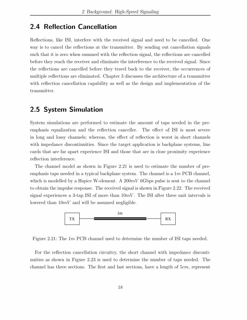
2.5 System Simulation
System simulations are performed to estimate the amount of taps needed in the pre-
emphasis equalization and the reflection canceller. The effect of ISI is most severe
in long and lossy channels; whereas, the effect of reflection is worst in short channels
with impedance discontinuities. Since the target application is backplane systems, line
cards that are far apart experience ISI and those that are in close proximity experience
reflection interference.
The channel model as shown in Figure 2.21 is used to estimate the number of pre-
emphasis taps needed in a typical backplane system. The channel is a 1m PCB channel,
which is modelled by a Hspice W-element. A 200mV 6Gbps pulse is sent to the channel
to obtain the impulse response. The received signal is shown in Figure 2.22. The received
signal experiences a 3-tap ISI of more than 10mV . The ISI after three unit intervals is
lowered than 10mV and will be assumed negligible.
RXTX
1m
Figure 2.21: The 1m PCB channel used to determine the number of ISI taps needed.
For the reflection cancellation circuitry, the short channel with impedance disconti-
nuities as shown in Figure 2.23 is used to determine the number of taps needed. The
channel has three sections. The first and last sections, have a length of 5cm, represent
18

2 Background: High-Speed Signaling
−1000 −500 0 500 1000 1500 2000 2500 3000 3500 4000 0
10
20
30
40
50
60
70
80
90
Time (ps)
Rec
eive
d V
olta
ge (
mV
)
3UI
3UI
1UI
2UI
Figure 2.22: The impulse response of a 1m PCB channel.
the length of the PCB trace on the line card. The 8cm middle section represents the
PCB channel on the backplane. The two 3pF capacitors represent the connectors used
to connect the line cards to the backplane. A 200mV 6Gbps pulse is sent to the channel
to obtain the impulse response as shown in Figure 2.24. The first reflection arrives at the
receiver after 1ns for a duration of about six unit intervals. The secondary reflections
caused by the first reflection are assumed to be negligible.
3pF
8cm
3pF
RXTX
5cm 5cm
Figure 2.23: The PCB channel used to determine the number of reflection taps needed.
19

2 Background: High-Speed Signaling
−1000 0 1000 2000 3000 4000 5000 6000−20
0
20
40
60
80
100
120
Time (ps)
Rec
eive
d V
olta
ge (
mV
)
6UI
6UI
Figure 2.24: The impulse response of a 8cm PCB channel with connectors.
The above system simulations indicate that for typical backplane systems, 3-tap pre-
emphasis equalization is adequate for 1m PCB channel at a data rate of 6Gbps. For
the reflections that occur in the short channels, between two adjacent line cards, the
number of taps should be more than six.
2.6 Summary
The frequency-dependent loss of PCB channels are caused by skin effect. Skin effect
manifests itself as ISI in the time-domain and causes interference to the received sig-
nal. Methods for canceling ISI include implementing pre-emphasis equalization in the
transmitter and implementing post-equalization in the receiver.
There are three different kinds of reflection: resistive, capacitive, and inductive. Re-
sistive reflection is the simplest to understand as the reflections have the same shape as
20

2 Background: High-Speed Signaling
the original signal. Capacitive and inductive reflections have different shapes due to the
time-dependent nature of capacitors and inductors.
21
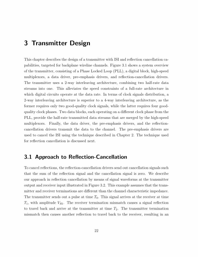
3 Transmitter Design
This chapter describes the design of a transmitter with ISI and reflection cancellation ca-
pabilities, targeted for backplane wireline channels. Figure 3.1 shows a system overview
of the transmitter, consisting of a Phase Locked Loop (PLL), a digital block, high-speed
multiplexors, a data driver, pre-emphasis drivers, and reflection-cancellation drivers.
The transmitter uses a 2-way interleaving architecture, combining two half-rate data
streams into one. This alleviates the speed constraints of a full-rate architecture in
which digital circuits operate at the data rate. In terms of clock signals distribution, a
2-way interleaving architecture is superior to a 4-way interleaving architecture, as the
former requires only two good-quality clock signals, while the latter requires four good-
quality clock phases. Two data blocks, each operating on a different clock phase from the
PLL, provide the half-rate transmitted data streams that are merged by the high-speed
multiplexors. Finally, the data driver, the pre-emphasis drivers, and the reflection-
cancellation drivers transmit the data to the channel. The pre-emphasis drivers are
used to cancel the ISI using the technique described in Chapter 2. The technique used
for reflection cancellation is discussed next.
3.1 Approach to Reflection-Cancellation
To cancel reflections, the reflection-cancellation drivers send out cancellation signals such
that the sum of the reflection signal and the cancellation signal is zero. We describe
our approach in reflection cancellation by means of signal waveforms at the transmitter
output and receiver input illustrated in Figure 3.2. This example assumes that the trans-
mitter and receiver terminations are different than the channel characteristic impedance.
The transmitter sends out a pulse at time T0. This signal arrives at the receiver at time
T1, with amplitude VR1. The receiver termination mismatch causes a signal reflection
to travel back and arrive at the transmitter at time T2. The transmitter termination
mismatch then causes another reflection to travel back to the receiver, resulting in an
22

3 Transmitter Design
Data
clk180
clk0
DriversPre−emphasis
Driver
TransmitterDigital Block
Hig
h−sp
eed
Mul
tiple
xors
CancellationDrivers
Reflection
PLL
Transmitter
Data Block
Transmitter
Data Block
To channel
Figure 3.1: System overview.
undesired signal at the receiver at time T3. The signal at time T3 with an amplitude of
VR3 is the interference that causes errors in signal detection.
(b) R1
V0
V0
0
0
mV
mV
T3
T0
T1
VR2
R3V
T2
Time
Time
Cancellation Signal
(a)
V
Figure 3.2: Approach to reflection cancellation. (a) Transmitter output. (b) Receiverinput.
To remove the interfering signal, the reflection cancellation drivers sends out a negative
23

3 Transmitter Design
pulse at time T2, as shown by the dashed line in Figure 3.2. The reflection canceling
pulse, with an amplitude equal to the reflected portion of the signal traveling back to
the receiver, cancels the reflection at the receiver. The reflection cancellation technique
is able to cancel the reflections that are within the unit interval, regardless if they are
coming from a resistive, a capacitive, or an inductive source.
The time resolution for the reflection cancellation is 1UI. This arrangement results in
ease of implementation since the system clock can be used to create the 1UI delayed data.
To design the reflection cancellation with a higher time resolution, a phase interpolation
scheme is needed to shift the cancellation signals within unit intervals. Due to the time
resolution limitation, any reflections that occur between unit intervals are only partially
cancelled. However, this does not disrupt the reflection cancellation since reflections in
the interval boundaries do not affect the vertical eye opening the most. The reflections in
the middle of the unit intervals, which affect the vertical eye opening, are cancelled with
the reflection-cancellation signals. Although this does not lead to perfect cancellation,
it results in significant improvement of the eye opening as we will see later in Section
4.2.1.
3.2 Top Level Description
The top level block diagram of the transmitter is shown in Figure 3.3. The diagram
includes all the major blocks inside the transmitter as well as their interconnections.
There are three major blocks: the transmitter digital block, the transmitter front-end,
and the PLL block. The transmitter digital block generates the data signals and passes
them to the transmitter front-end for transmission. The data rate of the transmitter
is 6Gbps. The transmitter has a 3-tap pre-emphasis driver, which is adequate for a
1m PCB channel as shown in Section 2.5. For reflection cancellation, it has an 8-tap
reflection canceller. This is an over-design as it was previous shown that only six taps are
needed in typical backplane systems. However, eight taps do provide more flexibilities
in dealing with complicated reflections. The PLL block provides the 3GHz clock signals
for the transmitter digital block. These major blocks are discussed in detail later in this
chapter.
All the data signals are differential. Throughout the thesis, the true and complement
of a differential signal are named as signal and signalx. Also, clk0 and clk180 represent
24
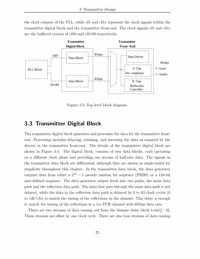
3 Transmitter Design
the clock outputs of the PLL, while clk and clkx represent the clock signals within the
transmitter digital block and the transmitter front-end. The clock signals clk and clkx
are the buffered version of clk0 and clk180 respectively.
Data Block
6Gbps
txout
txoutx
Data Driver
3−Tap
Pre−emphasis
8−Tap
ReflectionCanceller
3Gbpsclk0
clk180
PLL Block
3Gbps
TransmitterFront−End
TransmitterDigital Block
Data Block
Figure 3.3: Top level block diagram.
3.3 Transmitter Digital Block
The transmitter digital block generates and processes the data for the transmitter front-
end. Processing includes delaying, retiming, and inverting the data as required by the
drivers in the transmitter front-end. The details of the transmitter digital block are
shown in Figure 3.4. The digital block, consists of two data blocks, each operating
on a different clock phase and providing one stream of half-rate data. The signals in
the transmitter data block are differential, although they are shown as single-ended for
simplicity throughout this chapter. In the transmitter data block, the data generator
outputs data from either a 231 − 1 pseudo random bit sequence (PRBS) or a 128-bit
user-defined sequence. The data generator output feeds into two paths, the main data
path and the reflection data path. The data that goes through the main data path is not
delayed, while the data in the reflection data path is delayed by 0 to 63 clock cycles (0
to 126 UIs) to match the timing of the reflections in the channel. This delay is enough
to match the timing of the reflections in a 1m PCB channel with 6Gbps data rate.
There are two streams of data coming out from the dummy delay block txdat[1 : 0].
These streams are offset by one clock cycle. There are also four streams of data coming
25

3 Transmitter Design
DelayVariable Bit
Inversion
Bit
InversionAlignment
Negative
Negative
Alignment
txnneg[7:0]
txnpos[7:0]
txpos[3:1]
txneg[3:1]
txneg[0]
txpos[0]
txout
txoutx
txdat[1:0]
sclk
raw
txda
t
txdatn[3:0]
Mini−JTAG
Controller senLegend:
I/O pin
txdna[3:0]
Main Data Pathpr
bs_o
n, s
en
I/O SignalsJTAG
Reflection Data Path
clk0
clk180PLL Block
ControlTX
clk and clkx
for data blocks
Transmitter Digital Block
Data Block Sync with clk
Data Block Sync with clkx
driver_on, calseq_select
Transmitter
Front−End
(Section 3.4)
(Section 3.5)
txdnna[7:0]
DummyDelay
DataGenerator
Figure 3.4: The transmitter digital block.
out of the variable delay block txdatn[3 : 0], each with an additional clock cycle offset.
These offset data streams are retimed in the negative alignment blocks with the opposite
clock phase to produce 1/2 clock cycle (1UI) delayed data; data that is aligned with the
positive clock edge is retimed to the following negative clock edge. At the output of the
negative alignment block, two streams of output data, the original data stream and the
retimed data stream, are produced for one stream of input. In Figure 3.4, two streams
of data txdat[1 : 0] becomes four output streams txdna[3 : 0]. These 1UI offset data
streams then go through the bit inversion block. They are inverted, if needed, to allow
the pre-emphasis drivers and the reflection-cancellation drivers in the transmitter front-
end to produce negative cancellation signals. A total of twelve data streams, four from
the main data path txpos[3 : 0] and eight from the reflection data path txnpos[7 : 0],
26
3 Transmitter Design
are ready for the transmitter front-end. The four data streams from the main data path
go to the data driver, the 1st, 2nd and 3rd pre-emphasis drivers, while the eight data
streams from the reflection data path go to the eight reflection-cancellation drivers.
A control block and a mini-Joint Test Action Group (JTAG) controller are also in-
cluded in the transmitter digital block. The scan-clock sclk coming out of the mini-JTAG
scan-chain control block is sent to all the blocks that are in the scan-chain, which will be
discussed later in the chapter. The flip-flops of the data generator and those blocks with
the up-arrow sign use the system clock, clk and clkx. The system clock is multiplexed
between the scan-clock and the PLL clock, and one of them is selected depending on
the operation mode. The operation modes of the transmitter are covered in Chapter 4.
The sub-blocks of the transmitter digital block are discussed next.
3.3.1 Data Generator
The data generator, as shown in Figure 3.5, is made up of 128 cascaded flip-flops that
are connected in a ring architecture. The implementation of the flip-flops is discussed
later in Section 3.6.1. The 3-to-1 multiplexor, with a pair of control inputs, prbs on and
sen, selects one of the three functions of the data generator:
1. A section of the scan-chain in the transmitter
2. 231 − 1 Pseudo Random Bit Sequence (PRBS) generator
3. 128-bit circular shift register
Table 3.1 lists the data generator inputs and their corresponding functions. When
input sen is high, the data generator goes into scan-in mode and hence prbs on is
ignored. This generator architecture requires the least number of flip-flops to implement
all three functions since the PRBS generator shares the flip-flops with the 128-bit circular
shift register. The scan-chain within the data generator starts at the multiplexor sin
and ends at the 32nd flip-flop sout. The operation of the scan-chain is described later in
Section 3.3.7.
In the PRBS mode, the last thirty-one flip-flops are used to generate a 231 − 1 PRBS
with the initial seed pre-loaded during the scan-in process. Inputs to the XOR gate are
tapped from bit 0 and bit 3. Only two bits are chosen as the inputs to the XOR gate
because they are the minimum required to ensure that a maximum length sequence is
27

3 Transmitter Design
b127
clk clk
FF FF FF FF FF FF FFb0 rawtxdat
FF FF
sin
prbs
_on
sen
X1
00
10
31 FFsout
97 FF
buffer
Figure 3.5: The transmitter data generator.
Table 3.1: Data generator functions.
prbs on sen Functions
0 0 128-bit circular shift registerX 1 Scan-in mode1 0 231 − 1 PRBS
produced. As a result, the generator polynomial implemented is X32 +X3 +1 = 0. Part
of the resulting bit stream is shown in Table 3.2.
Table 3.2: PRBS sequence example.
State (b30 to b1) Output rawtxdat
000000000000000000000000001000 1100000000000000000000000000100 0110000000000000000000000000010 0011000000000000000000000000001 0001100000000000000000000000000 1
The 128-bit circular shift register is used for the transmission of the custom input
sequence and the calibration sequence. During this mode, the pre-loaded data is sent
out repeatedly. A long metal wire is required to connect the bit 0 flip-flop and the bit 127
flip-flop; thus, the last flip-flop has to drive the wiring capacitance of the long metal wire
as well as the input capacitance of the next stage. The buffer inserted in the feedback
28
3 Transmitter Design
path reduces the wiring capacitance that the last flip-flop has to drive. The outputs of
the data generator are fed to the main data path and the reflection data path.
3.3.2 Variable Delay Block
The variable delay block is used to generate the delayed version of the transmitted data
for the reflection-cancellation drivers. It has a 6-bit input from the scan-chain and can
delay the data by 0 to 63 clock cycles. Two possible implementations of the variable
delay block with only 2-to-1 multiplexors and flip-flops are shown in Figure 3.6. The
implementation in Figure 3.6(a) gives a constant delay path between the input and the
output, regardless of the delay selection. The delay path for this implementation is
always one multiplexor. However, the data input loading of this implementation can be
large since the input signal routes to all the multiplexors and one flip-flop.
We have chosen the implementation in Figure 3.6(b). This particular implementation
has the least amount of data input loading, that is one multiplexor and one flip-flop.
This increases the maximum operating speed of the data path since little buffering is
required for the data.
The disadvantage of this implementation is that the data goes through six multiplexors
in one clock cycle when zero delay is selected. Since the clock period is only 333ps, it
is impossible to meet the timing requirement with this implementation. To relax the
timing requirement, the data path is divided into three pipeline stages by the use of two
multiplexor flip-flops, labelled as ”MUX Flip-flop” in Figure 3.6(b). The ”MUX flip-
flop” is equipvalent to a 2-to-1 multiplexor cascaded by a flip-flop. The implementation
of the ”MUX flip-flop” is described later in Section 3.6.2.
The transmitter has eight reflection-cancellation drivers, which require eight streams
of data with 1UI spacing in the reflection data path. The four flip-flops at the output of
the variable delay block provide four data streams with one clock cycle spacing, and the
four data streams are further divided into the eight data streams with 1UI spacing in
the next stage. The output waveforms of the variable delay block are shown in Figure
3.7.
29

3 Transmitter Design
txdatn[0]
2FF1FF
4FF
8FF
16FF32FF
FF FF FF FF FFFF
FF
rawtxdat
sin
sclk
clk
sout
(b)
rawtxdat
txdatn
clk
(a)
delay_select
MUX Flip−flop
MUX Flip−flopMUX
MUX
MUXMUX
FF
FF FF
FF
FF
FF
FF
txdatn[1]
txdatn[2]
txdatn[3]
Figure 3.6: Variable delay block implemented with only 2-to-1 multiplexors and flip-flops. (a) Implementation with constant delay but large input loading. (b)Implementation with long zero-delay path but small input loading.
3.3.3 Dummy Delay Block
Since two multiplexor flip-flops are used in the variable delay block, two flip-flops are
inserted in the dummy delay block to align the main data path to the innate pipeline
delay of the variable delay block. The dummy delay block is shown in Figure 3.8.
30

3 Transmitter Design
txdatn[3]
0 1 2 3 4 5
0 1 2 3 4 5
0 1 2 3 4 5
0 1 2 3 4 5
0 1 2 3 4 5
Time
Signals
rawtxdat
clk
txdatn[0]
txdatn[1]
txdatn[2]
Figure 3.7: The timing diagram of the signals in the variable delay block.
FF FF FF FFrawtxdat
txdat[0]
txdat[1]
clk
ExtraExtra
Figure 3.8: The dummy delay block.
The main data path provides the data for the data driver and the three pre-emphasis
drivers. The data from txdat[0] is later split into 0UI and 1UI delayed data for the data
driver and the 1st pre-emphasis driver. The data from txdat[1] is delayed by one clock
cycle from txdat[0] and will be split into 2UI and 3UI delayed data for the 2nd and the
3rd pre-emphasis drivers.
3.3.4 Negative Alignment Block
The purpose of the negative alignment block is to realign the input data stream with
the opposite clock phase to create a 1UI delayed version of the input data. The block
diagram for the negative alignment block is shown in Figure 3.9.
To create a 1UI delayed version of the incoming data stream, the output of the first
flip-flop is fed into the second negative edge triggered flip-flop. The output dout0p5 is
31

3 Transmitter Design
FF
clk
FF
dout
dout0p5din
Figure 3.9: The negative alignment block.
retimed to the negative edge of the clock, which is 1UI delayed from the output dout.
The timing diagram of the operation is shown in Figure 3.10.
clk
0 1 2 3 4 5
0 1 2 3 4 5
0 1 2 3 4 5
Signals
dout
Time
dout0p5
din
Figure 3.10: The negative alignment block timing diagram.
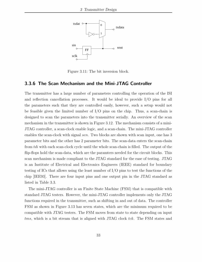
3.3.5 Bit Inversion Block
The bit inversion block inverts the data stream so that the pre-emphasis drivers and
reflection-cancellation drivers can create negative cancellation signals. The schematic of
the bit inversion block is illustrated in Figure 3.11.
The circuit is a 2-to-1 multiplexor. The implementation of the multiplexor is described
later in Section 3.6.3. The bit inversion block selects either txdat or its inverted value
from the incoming data stream, with the select input of the multiplexor coming from
the scan-chain. The differential implementation of the bit inversion block eliminates the
inverter by flipping the differential wires.
32
3 Transmitter Design
txdattxdata
sin
sclk
soutFF
1
0
Figure 3.11: The bit inversion block.
3.3.6 The Scan Mechanism and the Mini-JTAG Controller
The transmitter has a large number of parameters controlling the operation of the ISI
and reflection cancellation processes. It would be ideal to provide I/O pins for all
the parameters such that they are controlled easily, however, such a setup would not
be feasible given the limited number of I/O pins on the chip. Thus, a scan-chain is
designed to scan the parameters into the transmitter serially. An overview of the scan
mechanism in the transmitter is shown in Figure 3.12. The mechanism consists of a mini-
JTAG controller, a scan-clock enable logic, and a scan-chain. The mini-JTAG controller
enables the scan-clock with signal sen. Two blocks are shown with scan input, one has 3
parameter bits and the other has 2 parameter bits. The scan-data enters the scan-chain
from tdi with each scan-clock cycle until the whole scan-chain is filled. The output of the
flip-flops hold the scan-data, which are the paramters needed for the circuit blocks. This
scan mechanism is made compliant to the JTAG standard for the ease of testing. JTAG
is an Institute of Electrical and Electronics Engineers (IEEE) standard for boundary
testing of ICs that allows using the least number of I/O pins to test the functions of the
chip [IEE93]. There are four input pins and one output pin in the JTAG standard as
listed in Table 3.3.
The mini-JTAG controller is an Finite State Machine (FSM) that is compatible with
standard JTAG testers. However, the mini-JTAG controller implements only the JTAG
functions required in the transmitter, such as shifting in and out of data. The controller
FSM as shown in Figure 3.13 has seven states, which are the minimum required to be
compatible with JTAG testers. The FSM moves from state to state depending on input
tms, which is a bit stream that is aligned with JTAG clock tck. The FSM states and
33

3 Transmitter Design
Enable Logic
tdi tdo
sout sin
mini−JTAGController
tck
sen
sclkScan−chain
trst
Scan−clocktms
A block withA block with
3 parameter bits 2 parameter bits
Figure 3.12: Overview of the scan mechanism in the transmitter.
Table 3.3: JTAG pin list.
Pin Name Direction Functionstdi Input Scan-data inputtck Input JTAG clocktms Input Test mode selecttrst Input JTAG reset (optional)tdo Output Scan-data output
their functions are listed in Table 3.4. State ShDR enables the data scan-in by setting
sen to high, while the other states disable the scan-in process by setting sen to low.
The scan-clock sclk is a gated version of the JTAG clock tck; the gating is provided by
an AND-gate with sen being the enable signal. The signal trst is the signal to reset
the mini-JTAG controller back to the TLR state. The actual scan-chain is a chain
of flip-flops with a single input tdi and a single output tdo. In the transmitter, the
input and output of scan-chain sections within circuit blocks are named as sin and sout
respectively.
34

3 Transmitter Design
ShDR
1 0
0
1
1
0
0
0
1
0
1
1
0
1
Legend:
tms
TLRsen=0
RTIsen=0
SDRsen=0
CDRsen=0
sen=1EDRsen=0
UDRsen=0
Figure 3.13: The mini-JTAG controller FSM.
Table 3.4: FSM states representation and output.
State Output
State Name q2 q1 q0 sen Function
TLR 0 0 0 0 Reset state machineRTI 0 0 1 0 Idle stateSDR 0 1 0 0 Do nothingCDR 0 1 1 0 Do nothingShDR 1 0 0 1 Shift data in and out of the chipEDR 1 0 1 0 Do nothingUDR 1 1 0 0 Do nothing
Not Used 1 1 1 0
3.3.7 Scan-Chain
The scan-chain in the transmitter is shown in Figure 3.14. It goes through the major
blocks in the transmitter and sets the parameters for the blocks. The first section of the
scan-chain is in the data block synchronized with clk. The first part of the scan-chain is
the 128 flip-flops in the data generator. These flip-flops are shared between the data path
and the scan-chain since their initial states are set by the scan-in process. The next part
of the scan-chain is inside the variable delay block and it sets the 6-bit delay control
35

3 Transmitter Design
bit (MSB to LSB). The next section of the scan-chain sets the 8-bit and 4-bit invert
control signals for the reflection data path and the main data path. The scan-chain then
repeats itself for the data block that is synchronized with clkx. Next, the scan-chain
sets the 6-bit tap strength control (MSB to LSB) for the pre-emphasis drivers and the
reflection-cancellation drivers, starting with the 1st pre-emphasis driver and ending with
the 8th reflection-cancellation driver. The last two bits of the scan-chain are inside the
transmitter control block to set the transmitter operation mode as described in Section
3.3.8. Table 3.5 shows the bits assignment of the scan-chain in detail.
18 bits
Bit Inversion
(Main)
4 bits
Data VariableDelayGenerator
6 bits128 bits
Bit Inversion
(Reflection)
8 bits
2 bits48 bits
Bit Inversion
(Main)
4 bits
tdi
Data Block (clk)
Data Block (clkx)
tdoPre−
EmphasisReflectionCanceller
Data VariableDelayGenerator
6 bits128 bits
Bit Inversion
(Reflection)
8 bits
ControlBlock
Figure 3.14: The transmitter scan-chain.
3.3.8 Transmitter Control Block
The transmitter control block contains the control logic for the transmitter. It controls
the data driver, the data generator, and the calibration sequence enable pin in the high-
speed data multiplexors. The block diagram of the control block is shown in Figure
3.15.
The last two bits of the scan-chain are located in the transmitter control block, prbs
36

3 Transmitter Design
Table 3.5: Detailed scan-chain bit representation.
Bits Function Block Description
359:232 Data Generator 128-bit data generator231:226 Variable Delay 6-bit delay chain225:218 Bit Inversion 8-bit invert signal (reflection data path)217:214 Bit Inversion 4-bit invert signal (main data path)213:86 Data Generator 128-bit data generator85:80 Variable Delay 6-bit delay chain79:72 Bit Inversion 8-bit invert signal (reflection data path)71:68 Bit Inversion 4-bit invert signal (main data path)67:50 3-tap Pre-emphasis 3 6-bit pre-emphasis tap control49:2 8-tap Reflection Canceller 8 6-bit reflection tap control1:0 TX Control Block prbs and calibration bits
prbsCombination
Logic
calseq_select
driver_on
prbs_on
tdo
sclk
sin FF FF FF
calibration
Figure 3.15: The transmitter control block.
and calibration, and they are the only inputs to the combinational logic. Table 3.6
shows the truth table of the inputs and their corresponding outputs and functions. The
output prbs on is the PRBS select signal for the data generator, driver on is the enable
signal for the transmitter drivers, and calseq select is the calibration sequence enable
signal in the high-speed data multiplexors.
3.3.9 Transmitter Digital Block Layout
A testchip of the transmitter is implemented in Fujitsu’s 0.11µm CMOS process. The
layout of the transmitter digital block in the transmitter testchip is shown in Figure
3.16. The size of the layout is 550µm × 300µm. The digital block synchronized by clkx
37

3 Transmitter Design
Table 3.6: Transmitter control logic truth table.
Inputs Outputs
prbs calibration Operation Mode prbs on driver on calseq select
0 0 Custom Input 0 1 00 1 Calibration 0 1 11 0 PRBS 1 1 01 1 Driver Off 0 0 0
is at the top while the one synchronized by clk is placed at the bottom. The clock buffer
is placed in the middle of the chip. The negative alignment blocks and the bit inversion
blocks are placed after the delay blocks, and the data multiplexors, discussed in later in
Section 3.4.1, are placed in the right. In addition, the transmitter control logic is placed
at the bottom. The layout is optimized such that minimum length of wiring is needed
to connect the digital block to the transmitter front-end.
Figure 3.16: Transmitter digital block layout.
38

3 Transmitter Design
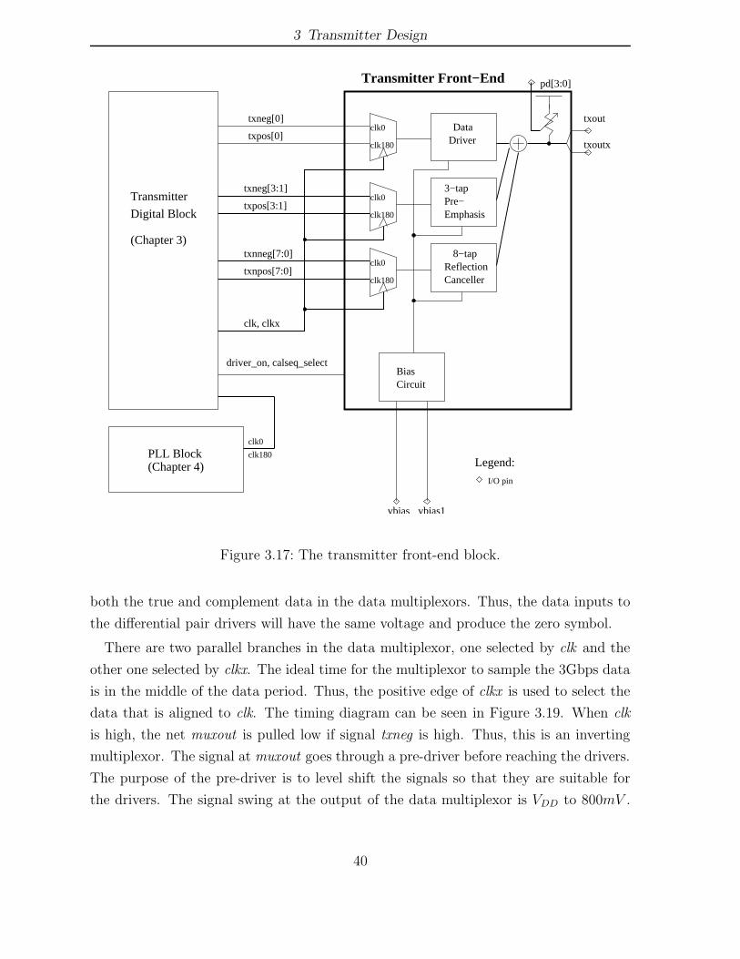
3.4 The Transmitter Front-End Block
The transmitter front-end, as shown in Figure 3.17, combines and transmits the data
from the digital block. Besides the normal data transmission, the transmitter front-
end provides ISI and reflection cancellation. In the transmitter front-end, there are six
blocks: the high-speed data multiplexors, the driver bias circuit, the data driver, the 3-
tap pre-emphasis driver, the 8-tap reflection canceller, and the 4-bit digitally controlled
variable termination resistors. The high-speed data multiplexors merge the data from
the transmitter digital block into a 6Gbps data stream. The data driver then transmits
the data stream onto the channel. The channel output is a current sum of the signals
from the data driver, the 3-tap pre-emphasis driver, and the 8-tap reflection canceller.
The 8 continuous taps of the reflection canceller can be delayed from 0 to 126 UIs
to match the timing of the reflections. The delay is provided by the variable delay
block, which was described in Section 3.3.2. The bias voltages of the current sources
for all the drivers are provided from a common bias circuit. To properly terminate the
channel at the transmitter end, a pair of 4-bit externally controlled PMOS resistors are
implemented. The following sections discuss the sub-blocks of the transmitter front-end
in detail.
3.4.1 High-Speed Data Multiplexor
High-speed multiplexors merge the data generated by the two transmitter data blocks
into a 6Gbps data stream for transmission. The data inputs to the data multiplexor,
txpos and txneg, in Figure 3.18 come from the output of the transmitter digital block.
The same data multiplexor is used for the complement of the differential data. Inputs
txpos and txneg are the 3Gbps data streams synchronized with the clk and clkx respec-
tively. Signals invpos and invneg in Figure 3.18 are enable signals for the calibration
mode. The calibration mode requires a zero symbol to obtain the channel characteristics.
The zero symbol has a voltage level midway between a ’1’ symbol and a ’-1’ symbol.
The calibration mode is discussed later in Chapter 4. Table 3.7 shows the truth table for
the invpos and invneg signals. Input signal invert comes from the bit inversion block in
the transmitter digital block and input calseq select comes from the transmitter control
block. If either the invpos or the invneg signal is pulled low, the transmitter goes into
the calibration mode. All the ’-1’ symbols are converted into zero symbols by disabling
39
3 Transmitter Design
CancellerReflection
8−tap
BiasCircuit
Legend:
clk180
clk0
clk180
clk0
clk180
clk0
txpos[0]
vbias vbias1
DataDriver
EmphasisPre−3−tap
clk, clkx
txneg[0]
txnpos[7:0]
txneg[3:1]
txpos[3:1]
txnneg[7:0]
txout
txoutx
clk0
clk180
I/O pin
Transmitter
Digital Block
(Chapter 3)
PLL Block(Chapter 4)
pd[3:0]Transmitter Front−End
driver_on, calseq_select
Figure 3.17: The transmitter front-end block.
both the true and complement data in the data multiplexors. Thus, the data inputs to
the differential pair drivers will have the same voltage and produce the zero symbol.
There are two parallel branches in the data multiplexor, one selected by clk and the
other one selected by clkx. The ideal time for the multiplexor to sample the 3Gbps data
is in the middle of the data period. Thus, the positive edge of clkx is used to select the
data that is aligned to clk. The timing diagram can be seen in Figure 3.19. When clk
is high, the net muxout is pulled low if signal txneg is high. Thus, this is an inverting
multiplexor. The signal at muxout goes through a pre-driver before reaching the drivers.
The purpose of the pre-driver is to level shift the signals so that they are suitable for
the drivers. The signal swing at the output of the data multiplexor is VDD to 800mV .
40

3 Transmitter Design
Table 3.7: Truth table for data multiplexor invpos and invneg pins.
Input Output
invert calseq select invpos invneg Functions0 0 1 1 Normal transmission0 1 1 0 Calibration mode1 0 1 1 Inverted normal transmission1 1 0 1 Invert calibration mode
Note: All transistor lengths are 0.11um unless indicated otherwise
16
10
16
16
16
10
5
5
20
40
0.33/0.5
clkx Pre−driver
muxout
outclk
txneg
invneg
txpos
invpos
Figure 3.18: The 6Gbps high-speed data multiplexor.
Simulation results show that the multiplexor output signal swing can fully switch the
current in the drivers.
3.4.2 Bias Circuit
A wide-swing cascode bias circuit [JM97] is used to provide the bias voltage for the cur-
rent sources of the data driver, the pre-emphasis drivers and the reflection-cancellation
drivers. This bias circuit has a simple implementation yet it provides a high output
impedance. The circuit is shown in Figure 3.20.
There are two inputs to this circuit, vbias and vbias1, and they both require an
41
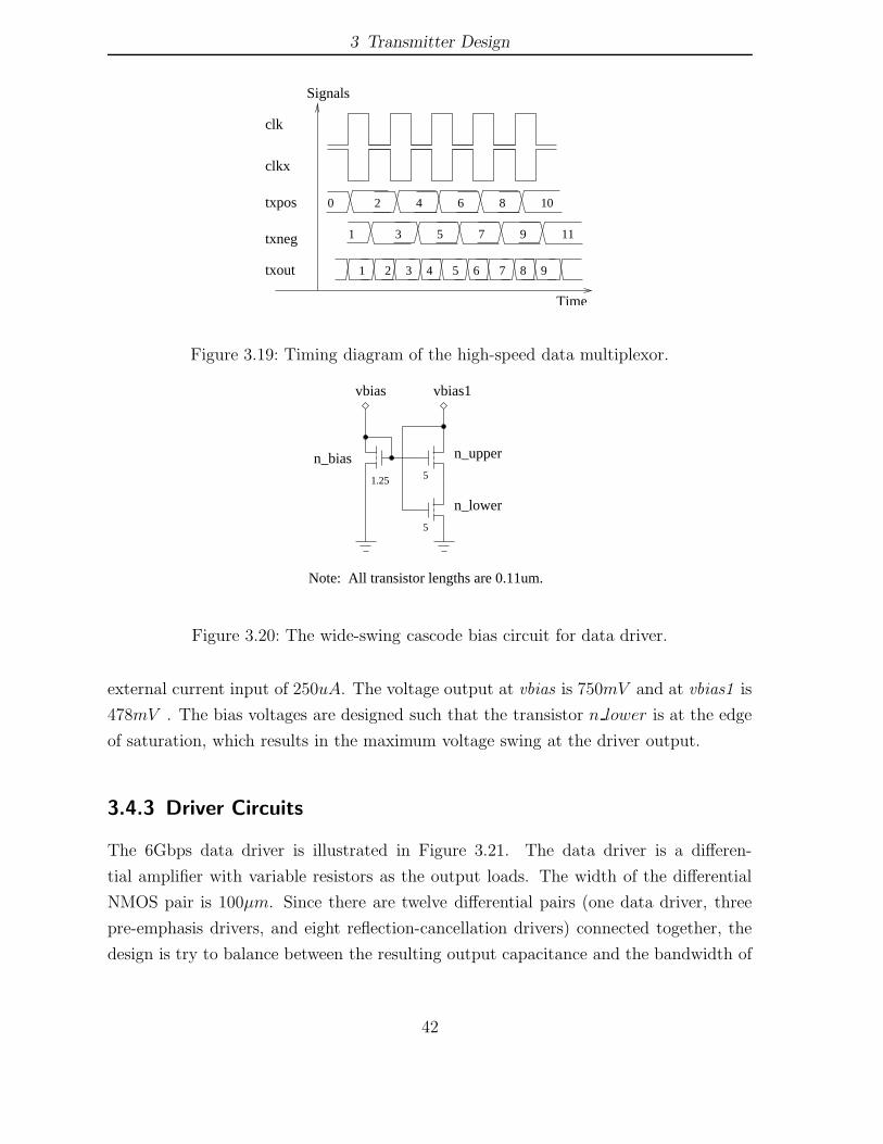
3 Transmitter Design
clk
3 5 7 9 11
0 2 4 6 8 10
1
1 2 3 4 5 6 7 8 9
Time
Signals
clkx
txpos
txneg
txout
Figure 3.19: Timing diagram of the high-speed data multiplexor.
Note: All transistor lengths are 0.11um.
1.25 5
5
vbias vbias1
n_lower
n_uppern_bias
Figure 3.20: The wide-swing cascode bias circuit for data driver.
external current input of 250uA. The voltage output at vbias is 750mV and at vbias1 is
478mV . The bias voltages are designed such that the transistor n lower is at the edge
of saturation, which results in the maximum voltage swing at the driver output.
3.4.3 Driver Circuits
The 6Gbps data driver is illustrated in Figure 3.21. The data driver is a differen-
tial amplifier with variable resistors as the output loads. The width of the differential
NMOS pair is 100µm. Since there are twelve differential pairs (one data driver, three
pre-emphasis drivers, and eight reflection-cancellation drivers) connected together, the
design is try to balance between the resulting output capacitance and the bandwidth of
42
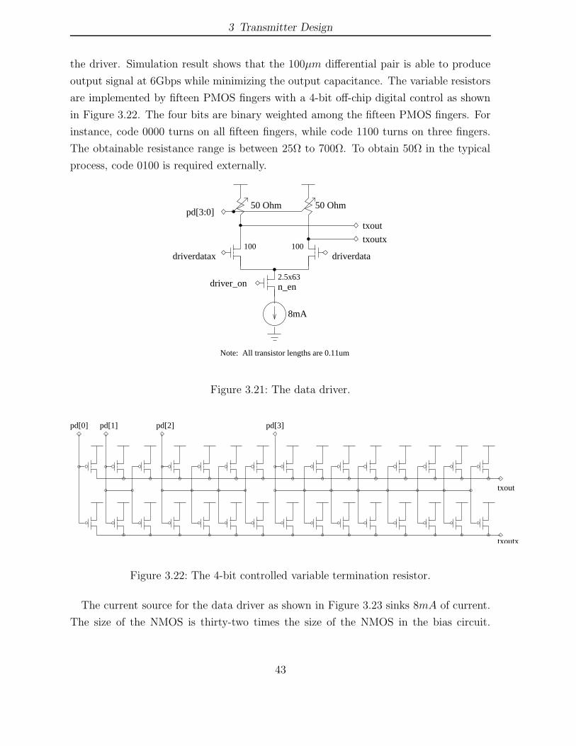
3 Transmitter Design
the driver. Simulation result shows that the 100µm differential pair is able to produce
output signal at 6Gbps while minimizing the output capacitance. The variable resistors
are implemented by fifteen PMOS fingers with a 4-bit off-chip digital control as shown
in Figure 3.22. The four bits are binary weighted among the fifteen PMOS fingers. For
instance, code 0000 turns on all fifteen fingers, while code 1100 turns on three fingers.
The obtainable resistance range is between 25Ω to 700Ω. To obtain 50Ω in the typical
process, code 0100 is required externally.
100
txout
pd[3:0]
driver_on2.5x63n_en
8mA
driverdatax
Note: All transistor lengths are 0.11um
100
50 Ohm50 Ohm
driverdata
txoutx
Figure 3.21: The data driver.
pd[3]
txout
txoutx
pd[0] pd[1] pd[2]
Figure 3.22: The 4-bit controlled variable termination resistor.
The current source for the data driver as shown in Figure 3.23 sinks 8mA of current.
The size of the NMOS is thirty-two times the size of the NMOS in the bias circuit.
43

3 Transmitter Design
The 8mA current produces an output swing of 200mV in a 50Ω channel. The 200mV
transmitted signal swing is the minimum required to produce a 100mV received signal
at the end of a 10m PCB trace at a data rate of 6Gbps. Transistor n en is the enable
switch for the data driver. When the driver is on, transistor n en is a small resistor and
does not interfere with the driver’s operation.
vbias1
Note: All transistor lengths are 0.11um
2.5x63
2.5x63
src
2.5x63
n_endriver_on
vbias
Figure 3.23: The current source for the data driver.
The schematics for the 3-tap pre-emphasis driver and 8-tap reflection-cancellation
driver are shown in Figure 3.24 and Figure 3.25 respectively. They are also implemented
by differential amplifiers. The current sources for the pre-emphasis drivers and the
reflection-cancellation drivers are different from the data driver as shown in Figure 3.26.
The 8mA current is divided into six binary weighted branches, and each branch has
a similar structure to the data driver current source. The 8mA current is an over-
design for the pre-emphasis drivers and the reflection cancellation drivers because ISI
and reflections cancellation signals normally have amplitude much less than the data
signals. However, the use of the same current source as the data driver saves design
time in the layout stage as it can be copied directly from the data driver current source.
The enable transistors are controlled by the scan-chain outputs.
44

3 Transmitter Design
txoutx
100 100
pu[5−0] 8mA
txdatx[0] txdat[0]
100 100
pu[11−6] 8mA
txdatx[1] txdat[1]
100 100
8mA
txdatx[2] txdat[2]
pu[17−12]
txout
Figure 3.24: The 3-tap pre-emphasis driver.
45

3Tra
nsm
itterD
esign
txout
100 100
pu[5−0] 8mA
100 100
pu[11−6] 8mA
txdatn[1]
100 100
8mA
txdatnx[3]
pu[23−18]
100 100
8mApu[17−12]
txdatn[2]txdatnx[2]txdatn[0] txdatnx[1]txdatnx[0] txdatn[3]
100 100
8mA
100 100
8mA
txdatn[5]
100 100
8mA
txdatnx[7]
pu[47−42]
100 100
8mApu[41−36]
txdatn[6]txdatnx[6]txdatn[4] txdatnx[5]txdatnx[4] txdatn[7]
pu[35−30]pu[29−24]
txoutx
Figu
re3.25:
The
8-taprefl
ection-can
cellationdriver.
46
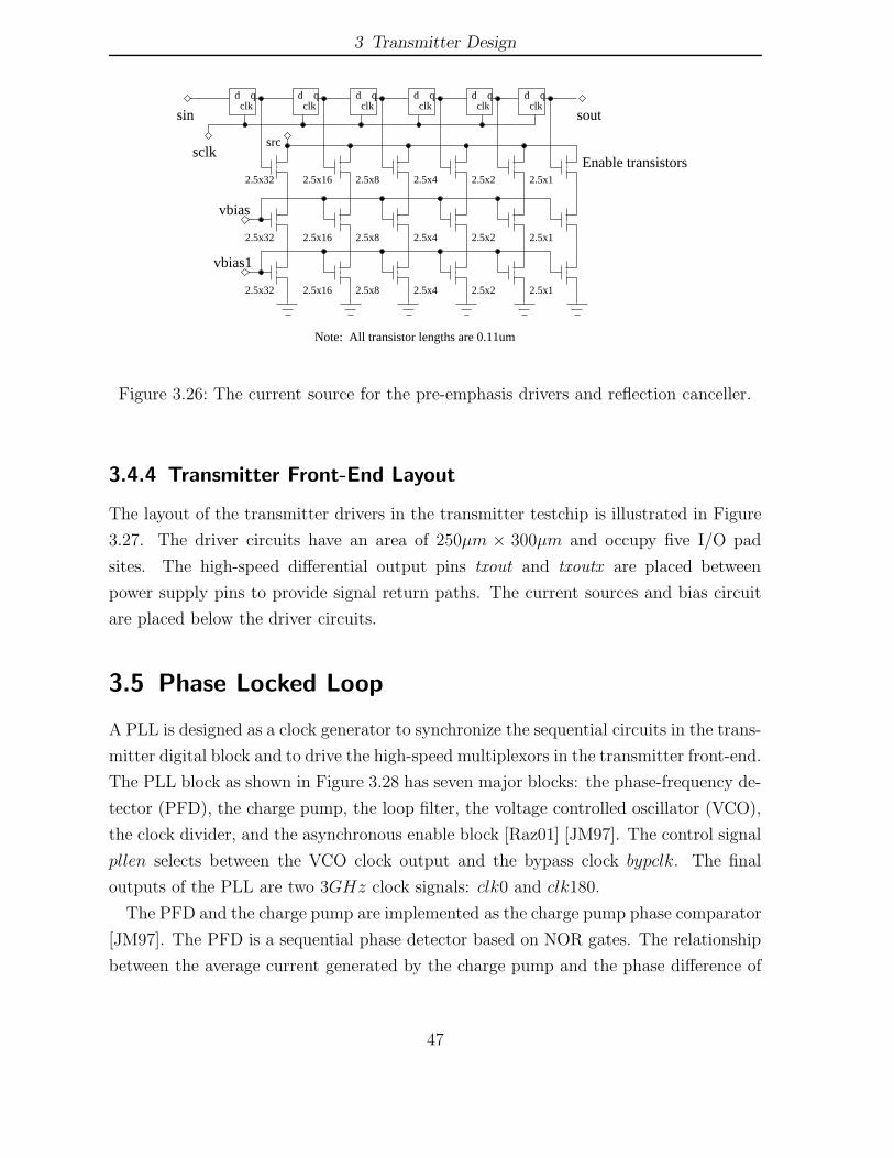
3 Transmitter Design
sclk
qclk
d qclk
d qclk
d qclk
dqclk
dqclk
d
Note: All transistor lengths are 0.11um
2.5x16
2.5x16
2.5x16
2.5x8
2.5x8
2.5x8
2.5x4
2.5x4
2.5x4
2.5x2
2.5x2
2.5x2
2.5x1
2.5x1
2.5x1
2.5x32
2.5x32
2.5x32
src
sin sout
Enable transistors
vbias
vbias1
Figure 3.26: The current source for the pre-emphasis drivers and reflection canceller.
3.4.4 Transmitter Front-End Layout
The layout of the transmitter drivers in the transmitter testchip is illustrated in Figure
3.27. The driver circuits have an area of 250µm × 300µm and occupy five I/O pad
sites. The high-speed differential output pins txout and txoutx are placed between
power supply pins to provide signal return paths. The current sources and bias circuit
are placed below the driver circuits.
3.5 Phase Locked Loop
A PLL is designed as a clock generator to synchronize the sequential circuits in the trans-
mitter digital block and to drive the high-speed multiplexors in the transmitter front-end.
The PLL block as shown in Figure 3.28 has seven major blocks: the phase-frequency de-
tector (PFD), the charge pump, the loop filter, the voltage controlled oscillator (VCO),
the clock divider, and the asynchronous enable block [Raz01] [JM97]. The control signal
pllen selects between the VCO clock output and the bypass clock bypclk. The final
outputs of the PLL are two 3GHz clock signals: clk0 and clk180.
The PFD and the charge pump are implemented as the charge pump phase comparator
[JM97]. The PFD is a sequential phase detector based on NOR gates. The relationship
between the average current generated by the charge pump and the phase difference of
47

3 Transmitter Design
Figure 3.27: Transmitter front-end layout.
clken
0
1
pllclk
dnvcntl
fbclk
bypclk
vcoclk
pllen
ClockDivider
1/32
VoltageControlledOscillator
LoopFilter
ChargePump
Phase
Frequency
Detector
upref_clkAsync
Enable
clk0
clk180
Figure 3.28: Top level PLL diagram.
the feedback and the reference clocks is simulated in Hspice. The plot is shown in Figure
3.29. The slope of the line represents the gain of the charge pump phase comparator,
48

3 Transmitter Design
which is equal to 9.86uA/rad in the typical process corner.
−6 −4 −2 0 2 4 6−100
−50
0
50
100
150
Phase Difference (rad)
Ave
rage
Cha
rge
Pum
p O
utpu
t Cur
rent
(m
A)
Typcal CornerSlow CornerFast Corner
Figure 3.29: Relationship between charge pump current and phase difference betweenref clk and fb clk.
The loop filter is a second order passive filter [Raz01]. A PLL needs to have damping
factor ζ = 0.707 to 1 for its transient response to be critically damped. For this loop
filter, ζ is designed to be 0.8915. With this loop filter, the bandwidth of the PLL is
11.7MHz.
The oscillator of the PLL is a tuned LC-VCO modified from [AM00] as shown in
Figure 3.30. It is implemented with an inductor, a varactor, and a negative Gm stage.
The inductor has an inductance of 1nH. The varactor is implemented with NMOS
transistors with their drain and source nodes shorted together. The VCO has a centre
frequency of 3GHz. The range of the control voltage goes from 0V to 1.2V , with a
linear tuning region between 0.3V to 0.9V . As shown in Figure 3.31, the tuning range
of the VCO is between 2.5GHz to 3.8GHz. The gain of the VCO, KV CO, is equal to
the slope of the tangent line at Vcntl = 0.6V . In the typical process corner, the gain of
the VCO is 1.66GHz/V .
In this PLL, the VCO clock frequency is divided by thirty-two using five cascaded
flip-flops. The clock divider schematic is shown in Figure 3.32. The challenge in this
49

3 Transmitter Design
vctrl
vcooutx
vcobias
psrcpref
psrc
vcoout
Output Stage
Figure 3.30: LC-VCO Block.
0 0.2 0.4 0.6 0.8 1 1.2 1.42.4
2.6
2.8
3
3.2
3.4
3.6
3.8
4
Vctrl
(V)
Osc
illat
ion
Freq
uenc
y (G
Hz)
Typcal CornerSlow CornerFast Corner
Figure 3.31: VCO tuning range.
50

3 Transmitter Design
design is to ensure that the flip-flop in the first stage responds fast enough to work with
the PLL clock output. From extracted simulation, the clock divider can work up to
4GHz in all process corners.
clk
FF
clk
FF
clk
FF
clk
FF
clk
FF
vcoclk
fbclk
Figure 3.32: The schematic of the clock divider.
The PLL clock output is gated by an external clock enable signal clken (refer to Figure
3.28). The asynchronous enable block retimes the signal clken internally to ensure that
a glitchless clock cycle is sent to the transmitter digital block when the clock signals are
enabled. The schematic of the asynchronous enable block is illustrated in Figure 3.33.
FF
FF
pllclkx
FFclk0
pllclk
clken
clk180
syn180
syn0
Gate
Gate
Figure 3.33: The schematic of the asynchronous enable block.
The asynchronous enable block uses two negative-edge triggered flip-flops to retime
the signal clken. The output of the flip-flops syn0 becomes the internal enable signal
for the clock clk. Since the flip-flop is negative-edge triggered, it guarantees that signal
syn0 is high before the clock cycle begins. Thus, it ensures that the first clock pulse
sent to the transmitter digital block is a full clock cycle.
51

3 Transmitter Design
To ensure that clk0 is leading clk180, clk0 is used to generate the internal enable
signal for clk180. In Figure 3.33, the internal enable signal for clk180 is syn180. The
timing of these signals is shown in Figure 3.34. Signal syn0 goes high after two negative
edges of pllclk, and signal syn180 enables clk180 after clk0 goes high.
Time
pllclk
pllclkx
clken
syn0
clk0
syn180
clk180
Signals
Figure 3.34: The asynchronous enable block circuit timing diagram.
3.5.1 PLL Layout
The 3GHz PLL layout in the transmitter testchip is shown in Figure 3.35. The size of
the layout is 250µm× 300µm. The LC-VCO is drawn with perfect symmetry to ensure
the differential output of the VCO is balanced. As expected, the layout of the inductor
and the loop filter occupied most of the area. In addition, the inductor is placed 20µm
from other circuits to minimize coupling.
3.6 Primitive Circuits
This section presents the implementation of the primitive circuits in the transmitter.
Three main primitive circuits are used in the design: the sense-amplifier flip-flop, the
52

3 Transmitter Design
Figure 3.35: 3GHz PLL layout.
sense-amplifier multiplexor flip-flop, and the 2-to-1 multiplexor. The design and imple-
mentation of these circuits are presented in the following sections.
3.6.1 Sense-Amplifier Flip-Flop
The timing of the digital data in the transmitter is synchronized by a 3GHz clock. Due
to the high-speed operation, conventional master-slave flip-flops cannot meet the timing
requirements. As a result, the sense-amplifier flip-flop in Figure 3.36 is selected because
of its ability to work with high-speed signals [NSO99].
The operation of the flip-flop is divided into two phases: the reset phase and the latch
53

3 Transmitter Design
n_fbd dx
pdrv
nsrc sx
qx
ndrv
q
clk rx
r s
pprechg
SenseAmplifier
Latch
n_fb
Figure 3.36: The sense-amplifier flip-flop.
phase. The flip-flop goes into the reset phase when clk is low and into the latch phase
when clk is high. In the reset phase, the sense-amplifier is pre-charged, and any change
from the flip-flop inputs, d and dx, is isolated from the flip-flop outputs, q and qx. At
the same time, the latch retains the result from the previous latch phase and drives the
flip-flop outputs. In the latch phase, the sense-amplifier amplifies the difference between
the differential inputs d and dx. The result is written into the latch to drive the flip-flop
outputs.
The sense-amplifier flip-flop has a clk-q delay of 90ps. The output latch is designed to
charge an output load of 36fF , assuming a fan-out of four. The clock input capacitance
is 9fF , while the hold time of the flip-flop is 15ps. The sense-amplifier flip-flop requires
only a single phase clock. This reduces the clock loading of the transmitter, and ease
54

3 Transmitter Design
the clock signals routing.
3.6.2 Sense-Amplifier Multiplexor Flip-Flop
The sense-amplifier multiplexor flip-flop has the same structure as the sense-amplifier
flip-flop described in Section 3.6.1. However, there is a 2-to-1 multiplexor built into the
input stage of the sense-amplifier, which is equilvalent to a 2-to-1 multiplexor cascaded
in front of a sense-amplifier flip-flop. The schematic is shown in Figure 3.37.
qx
4
d1 d0 d0x d1x
s
clk
reset
dint dxint
pprechg
set
nsrc setx
resetx
pdrv
ndrv
q
Figure 3.37: The combined 2-to-1 multiplexor and sense-amplifier flip-flop.
The select input s multiplexes the input data into the sense-amplifier. It selects either
d0 and d0x or d1 and d1x as the inputs to the sense-amplifier. The internal capacitance
at nodes dint and dxint of the sense-amplifier is larger due to the connection of two extra
NMOS transistors. As a result, the clk-q delay is 110ps, slightly larger than the original
55
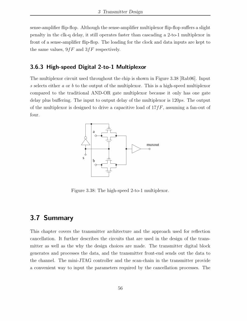
3 Transmitter Design
sense-amplifier flip-flop. Although the sense-amplifier multiplexor flip-flop suffers a slight
penalty in the clk-q delay, it still operates faster than cascading a 2-to-1 multiplexor in
front of a sense-amplifier flip-flop. The loading for the clock and data inputs are kept to
the same values, 9fF and 3fF respectively.
3.6.3 High-speed Digital 2-to-1 Multiplexor
The multiplexor circuit used throughout the chip is shown in Figure 3.38 [Rab96]. Input
s selects either a or b to the output of the multiplexor. This is a high-speed multiplexor
compared to the traditional AND-OR gate multiplexor because it only has one gate
delay plus buffering. The input to output delay of the multiplexor is 120ps. The output
of the multiplexor is designed to drive a capacitive load of 17fF , assuming a fan-out of
four.
sb
a
muxout
Figure 3.38: The high-speed 2-to-1 multiplexor.
3.7 Summary
This chapter covers the transmitter architecture and the approach used for reflection
cancellation. It further describes the circuits that are used in the design of the trans-
mitter as well as the why the design choices are made. The transmitter digital block
generates and processes the data, and the transmitter front-end sends out the data to
the channel. The mini-JTAG controller and the scan-chain in the transmitter provide
a convenient way to input the parameters required by the cancellation processes. The
56

3 Transmitter Design
PLL that is used as a clock generator is covered in detail. The PLL provides a differ-
ential 3GHz clock output for the transmitter. Finally, the primitive circuits such as
the sense-amplifier flip-flop and 2-to-1 multiplexor are described. The following chapter
presents the system operation modes and the simulation results.
57

4 System Operation Modes and Simulation
Results
This chapter discusses the transmitter operation modes and the system simulation re-
sults. Before data transmission, the channel characteristics must be obtained. From
the channel characteristics, the ISI and reflection-cancellation parameters need to be
adjusted properly. The process of obtaining the channel characteristics, adjusting the
parameters, and transmitting data are done in different operation modes. The simu-
lation results presented in the chapter show the effectiveness of the reflection and ISI
cancellation through the use of eye diagrams.
4.1 System Operation Modes
There are three different operation modes in the transmitter: the scan-in mode, the
calibration mode, and the data transmission mode. The scan-in mode loads the trans-
mitter scan-chain with the scan-in data sequence. The calibration mode sends out the
calibration sequence to obtain the channel characteristics. Finally, the data transmission
mode sends the data to the channel. The details of these operation modes are explained
in the following.
4.1.1 Scan-in Mode
In the scan-in mode, the transmitter loads in a 360-bit data sequence for the scan-chain.
This includes the initial sequence for the data generator (256 bits), the control bits for
the variable delay block (12 bits), the control bits for the bit inversion block (24 bits),
the control bits for the amplitude of the pre-emphasis and the reflection-cancellation
drivers (66 bits), and the control bits for the operation modes (2 bits). During the
scan-in mode, the PLL output is disabled until the data sequence is loaded into the
scan-chain.
58
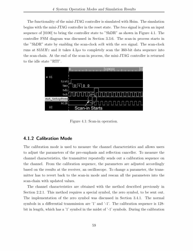
4 System Operation Modes and Simulation Results
The functionality of the mini-JTAG controller is simulated with Hsim. The simulation
begins with the mini-JTAG controller in the reset state. The tms signal is given an input
sequence of [0100] to bring the controller state to ”ShDR” as shown in Figure 4.1. The
controller FSM diagram was discussed in Section 3.3.6. The scan-in process starts in
the ”ShDR” state by enabling the scan-clock sclk with the sen signal. The scan-clock
runs at 83MHz and it takes 4.3µs to completely scan the 360-bit data sequence into
the scan-chain. At the end of the scan-in process, the mini-JTAG controller is returned
to the idle state ”RTI”.
Figure 4.1: Scan-in operation.
4.1.2 Calibration Mode
The calibration mode is used to measure the channel characteristics and allows users
to adjust the parameters of the pre-emphasis and reflection canceller. To measure the
channel characteristics, the transmitter repeatedly sends out a calibration sequence on
the channel. From the calibration sequence, the parameters are adjusted accordingly
based on the results at the receiver, an oscilloscope. To change a parameter, the trans-
mitter has to revert back to the scan-in mode and rescan all the parameters into the
scan-chain with updated values.
The channel characteristics are obtained with the method described previously in
Section 2.2.1. This method requires a special symbol, the zero symbol, to be sent out.
The implementation of the zero symbol was discussed in Section 3.4.1. The normal
symbols in a differential transmission are ’1’ and ’-1’. The calibration sequence is 128-
bit in length, which has a ’1’ symbol in the midst of ’-1’ symbols. During the calibration
59
4 System Operation Modes and Simulation Results
mode, the transmitter front-end converts all the ’-1’ symbols into zero symbols.
Using this method, the amount of ISI is determined by directly observing the output
waveform. By adjusting the amplitude of the pre-emphasis taps, ISI with up to 3UI du-
ration can be cancelled. The amount of signal reflection is determined also by observing
the output waveform. The coefficients of the 8-tap reflection canceller are adjusted such
that the reflections are completely removed or are zeroed out in the middle of the unit
interval. The timing of the reflection-cancellation signal is adjusted by setting the 6-bit
variable delay control. The timing of the 8-tap is adjusted such that it covers the entire
duration of the reflection. If that is not possible, the taps are adjusted to eliminate the
most dominant reflection. The simulation result of the calibration mode is shown along
with the result of the reflection and ISI cancellation later in this chapter.
4.1.3 Data Transmission Mode
Data transmission begins after calibration is completed. The transmitter is able to
transmit two different sequences of data: the 231 − 1 bit PRBS and the 128-bit user-
defined sequence. Their initial values are loaded into the data generator during the
scan-in mode. The simulation result of the data transmission is shown as received signal
eye diagrams later in this chapter.
4.2 Simulation Results
The extracted netlist of the transmitter is simulated in Hspice to demonstrate the ca-
pability of the reflection-cancellation circuitry. Two simulations, each with a different
channel, are presented here: one has severe termination impedance mismatches, and the
other includes two inductors. Also, simulations for ISI-cancellation are done separately
by using a lossy channel. The received signal eye diagrams, before and after cancellation,
are compared in all simulations.
4.2.1 Reflection Cancellation
The reflection-cancellation capability of the transmitter is demonstrated by simulating
the transmitter with a channel that includes impedance mismatches. The transmitter is
simulated in the calibration mode at 6Gbps to obtain the channel impulse response. The
60
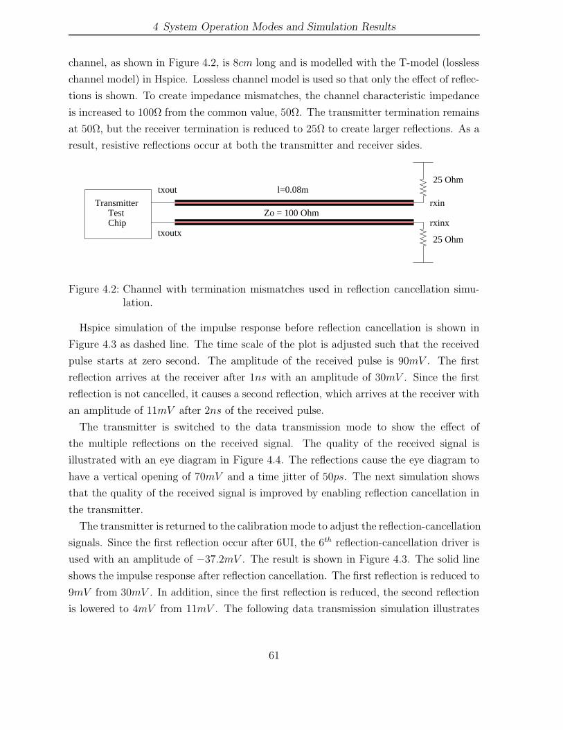
4 System Operation Modes and Simulation Results
channel, as shown in Figure 4.2, is 8cm long and is modelled with the T-model (lossless
channel model) in Hspice. Lossless channel model is used so that only the effect of reflec-
tions is shown. To create impedance mismatches, the channel characteristic impedance
is increased to 100Ω from the common value, 50Ω. The transmitter termination remains
at 50Ω, but the receiver termination is reduced to 25Ω to create larger reflections. As a
result, resistive reflections occur at both the transmitter and receiver sides.
TransmitterTestChip
txout
txoutx
l=0.08m25 Ohm
25 Ohm
rxin
rxinxZo = 100 Ohm
Figure 4.2: Channel with termination mismatches used in reflection cancellation simu-lation.
Hspice simulation of the impulse response before reflection cancellation is shown in
Figure 4.3 as dashed line. The time scale of the plot is adjusted such that the received
pulse starts at zero second. The amplitude of the received pulse is 90mV . The first
reflection arrives at the receiver after 1ns with an amplitude of 30mV . Since the first
reflection is not cancelled, it causes a second reflection, which arrives at the receiver with
an amplitude of 11mV after 2ns of the received pulse.
The transmitter is switched to the data transmission mode to show the effect of
the multiple reflections on the received signal. The quality of the received signal is
illustrated with an eye diagram in Figure 4.4. The reflections cause the eye diagram to
have a vertical opening of 70mV and a time jitter of 50ps. The next simulation shows
that the quality of the received signal is improved by enabling reflection cancellation in
the transmitter.
The transmitter is returned to the calibration mode to adjust the reflection-cancellation
signals. Since the first reflection occur after 6UI, the 6th reflection-cancellation driver is
used with an amplitude of −37.2mV . The result is shown in Figure 4.3. The solid line
shows the impulse response after reflection cancellation. The first reflection is reduced to
9mV from 30mV . In addition, since the first reflection is reduced, the second reflection
is lowered to 4mV from 11mV . The following data transmission simulation illustrates
61

4 System Operation Modes and Simulation Results
0 500 1000 1500 2000 2500 3000−20
0
20
40
60
80
100
Time (ps)
Vol
tage
of
(rxi
n, r
xinx
) (m
V)
Before reflection cancellationAfter reflection cancellation
3UI
90mV received pulse
6UI, 9mV
12UI, 4mV
Figure 4.3: The channel impulse response before and after reflection cancellation.
that significant improvment is made in the eye diagram by using reflection cancellation.
The transmitter is simulated in the data transmission mode with reflection cancella-
tion enabled. The received signal eye diagram is shown in Figure 4.5. It can be seen
that the vertical eye opening is increased to 140mV from 70mV , and the time jitter is
lowered to 30ps from 50ps prior to reflection cancellation. This simulation shows that
the transmitter is able to operate and produce relatively clean signal at the receiver
under severe termination mismatched channels.
To further demonstrate the reflection cancellation capability of the transmitter, a
channel with two impedance discontinuities is created. The channel, as shown in Figure
4.6, consists of three 4cm segments of a 12cm lossless transmission line and two 4nH
inductors for creating impedance discontinuities. The size of the inductors is intention-
ally enlarged to worsen the reflections in the channel. Finally, the channel is properly
terminated at both the transmitter and the receiver side with 50Ω resistors.
62
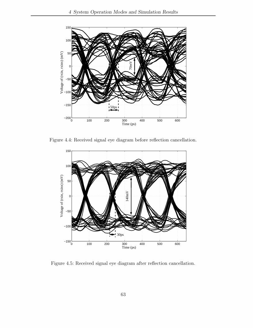
4 System Operation Modes and Simulation Results
0 100 200 300 400 500 600−200
−150
−100
−50
0
50
100
150
Time (ps)
Vol
tage
of
(rxi
n, r
xinx
) (m
V)
70m
V
50ps
Figure 4.4: Received signal eye diagram before reflection cancellation.
0 100 200 300 400 500 600−150
−100
−50
0
50
100
150
Time (ps)
Vol
tage
of
(rxi
n, r
xinx
) (m
V)
140m
V
30ps
Figure 4.5: Received signal eye diagram after reflection cancellation.
63

4 System Operation Modes and Simulation Results
txout
txoutx
rxinZo = 50 Ohm Zo = 50 Ohm Zo = 50 Ohm
l=0.04m l=0.04m
rxinx
TransmitterTestChip
l=0.04m
4nH
4nH 4nH
4nH
50 Ohm
50 Ohm
Figure 4.6: Channel with impedance discontinuities used in reflection cancellation sim-ulation.
Initially, the transmitter sends the calibration sequence on the channel with both
the pre-emphasis drivers and the reflection-cancellation drivers disabled. The received
signal before reflection cancellation is shown in Figure 4.7 as dashed line. The time axis
is scaled such that the received pulse starts at zero second. As expected, one inductive
reflection goes back to the receiver and arrives 500ps after the received pulse. This
reflection, if not cancelled, causes signal detection errors.
To show how the received signal is affected by the reflection, the transmitter is sim-
ulated in the data transmission mode. The transmitted data is sent to the channel at
6Gbps with an amplitude of 400mV . The eye diagram of the received signal presented
in Figure 4.8 shows the effect of the reflections. Signal reflections interfere with the
received signal and cause the eye diagram to have 80mV of vertical eye opening and
100ps of time jitter.
The eye diagram can be improved by reducing the reflections that travel back to
the receiver. With the transmitter operating in the calibration mode, the calibration
sequence is sent to the channel. The inductive reflection has a positive portion that
occurs at 600ps and a negative portion at 700ps as shown in Figure 4.7. The positive
portion occurs approximately 4UI after the main received pulse so the 4th reflection-
cancellation driver is used with an amplitude of −37.2mV . For the negative portion of
the inductive reflection, the 5th reflection-cancellation driver is used with an amplitude
of 27.9mV . By tuning the two reflection-cancellation drivers, the optimal result of the
calibration is shown in Figure 4.7. Since the reflections do not occur in the middle of
the unit interval, they cannot be fully cancelled. The positive portion is reduced from
42mV to 19mV , and the negative portion is lowered from −30mV to −21mV .
After the calibration, the transmitter is switched back to the data transmission mode.
64

4 System Operation Modes and Simulation Results
−500 0 500 1000 1500 2000 2500 3000 3500−40
−20
0
20
40
60
80
100
120
140
160
Time (ps)
Vol
tage
of
(rxi
n, r
xinx
) (m
V)
Before reflection cancellationAfter reflection cancellation
140mV received pulse
4UI, 19mV
5UI, −21mV
3UI
Figure 4.7: The channel impulse response before and after reflection cancellation.
The received signal eye diagram is shown in Figure 4.9. The eye diagram shows larger
eye openings than the one without reflection cancellation. The vertical eye opening has
increased to 160mV and the time jitter has decreased to 75ps. As a result, the reflection-
cancellation scheme improves the signal quality at the receiver by having larger received
signal amplitude and reduced time jitter.
4.2.2 ISI Cancellation
The ISI cancellation capability of the transmitter is demonstrated by simulating the
transmitter with the low-pass channel as shown in Figure 4.10. The low-pass charac-
teristic of the channel is represented by the first order RC filter with a -3dB frequency
of 2.1GHz such that adequate ISI is produced. The pair of 50Ω resistors are used for
termination to provide a 25Ω loading at the transmitter outputs. The ideal buffer is
65

4 System Operation Modes and Simulation Results
0 100 200 300 400 500 600−400
−300
−200
−100
0
100
200
300
400
Time (ps)
Vol
tage
of
(rxi
n, r
xinx
) (m
V)
100ps 80
mV
Figure 4.8: Received signal eye diagram before reflection cancellation.
0 100 200 300 400 500 600−300
−200
−100
0
100
200
300
Time (ps)
Vol
tage
of
(rxi
n, r
xinx
) (m
V)
160m
V
75ps
Figure 4.9: Received signal eye diagram after reflection cancellation.
66
4 System Operation Modes and Simulation Results
used to separate the transmitter with the channel output. This setup is similar to a sim-
ulation with the transmitter and a Hspice W-element model; however, the simulation
time is shortened since the signal propagation time is ignored.
1Transmitter
TestChip
txout
txoutx
50 Ohm
50 Ohm
rxin
rxinx
30 Ohm
30 Ohm2.5pF
2.5pF
Figure 4.10: Channel model used in ISI cancellation simulation.
To obtain the channel impulse response, the transmitter sends the calibration sequence
on the channel. The received pulse before ISI cancellation is shown in Figure 4.11 as
dashed line. The time axis is shifted such that the received pulse starts at zero seconds.
The received signal has an amplitude of 140mV , which is attenuated from a 200mV
transmitted pulse. The tail of the received signal extends until 500ps, and it causes a
30mV ISI after one unit interval.
The transmitter is then simulated in the data transmission mode with ISI cancellation
disabled. The received signal eye diagram is shown in Figure 4.12. The eye diagram
has a vertical opening of 200mV and a time jitter of 25ps. ISI cancellation can help
to enlarge the eye opening by lowering the amplitude of the transmitted signal and
emphasizing the signal transitions.
The transmitter is switched back to the calibration mode to find the optimal amplitude
of the pre-emphasis signals for ISI cancellation. Simulation shows that the optimal
received signal results when the amplitude of the first pre-emphasis driver is set to
−47.55mV . Figure 4.11 shows the impulse response of the channel after ISI cancellation.
The ISI after one unit interval is reduced to less than 10mV .
To show the improvment of the ISI cancellation on the received signal, the transmitter
is simulated in the data transmission mode with the pre-emphasis driver enabled. Figure
4.13 shows the eye diagram of the received signal, which has an eye opening of 300mV
and a time jitter of less than 25ps, compared to 200mV and 25ps respectively prior to
ISI cancellation. This shows that ISI cancellation has improved the eye opening of the
67

4 System Operation Modes and Simulation Results
0 500 1000 1500 2000−20
0
20
40
60
80
100
120
140
160
Time (ps)
Vol
tage
of
(rxi
n, r
xinx
) (m
V)
Before ISI cancellationAfter ISI cancellation
3UI
140mV received pulse
1UI, <10mV
Figure 4.11: The channel impulse response before and after ISI cancellation.
received signal.
4.2.3 Power Consumption
The power consumption of the transmitter, excluding the PLL, is simulated to be
297.3mW per channel in the typical condition. The contribution of each circuit block
to the total power consumption is shown in Figure 4.14. More than half of the trans-
mitter power (55%) is comsumed in the data generator due to the use of a large number
of flip-flops (256 in total). The variable delay block consumes 81mW (27%) from the
flip-flops (128 in total) used to delay the transmitted data. The rest of the circuits in
the digital block and the transmitter front-end contribute 16% to the total transmitter
power consumption. The power consumption of the pre-emphasis driver and the reflec-
tion cancellation driver is assumed to have a combined tail current of 5.25mA, which is
68

4 System Operation Modes and Simulation Results
0 100 200 300 400 500 600−250
−200
−150
−100
−50
0
50
100
150
200
250
Time (ps)
Vol
tage
of
(rxi
n, r
xinx
) (m
V)
25ps
200m
V
Figure 4.12: Received signal eye diagram before ISI cancellation.
0 100 200 300 400 500 600−200
−150
−100
−50
0
50
100
150
200
Time (ps)
Vol
tage
of
(rxi
n, r
xinx
) (m
V)
300m
V
<25ps
Figure 4.13: Received signal eye diagram after ISI cancellation.
69

4 System Operation Modes and Simulation Results
the amount of current used to cancel the reflection in the channel as shown previously
in Figure 4.10.
& Reflection Canceller
DigitalBlock
(9.1%)27mW163mW
(55%)81mW(27%)
Data Generator BlockVariable Delay
(3.4%)10mW
(3.4%)10mW
(2.1%)6.3mW
Data Multiplexors
Driver+Bias
Pre−emphasis
Rest of
Figure 4.14: Contributions of the transmitter power consumption.
In a production chip, the data generator is not needed, and hence its power consump-
tion should not be included when measuring the total power consumption. Thus, the
estimated power consumption in a production chip is only 134mW per channel.
4.3 PLL Simulation
The extracted netlist of the 3GHz PLL is simulated for lock acquisition and phase noise.
Lock acquisition simulation ensures that the PLL is able to acquire phase and frequency
locking between the frequency-divided VCO clock and the external reference clock. With
the control voltage initialized to 0V , the PLL is simulated until the VCO control voltage
reaches a stable value to ensure phase and frequency locking. Phase noise simulation is
then done to measure how the noise that is generated by the PLL components and the
reference clock affects the PLL output. From the PLL phase noise plot, the Root Mean
Square (RMS) jitter of the PLL is measured.
4.3.1 PLL Lock Acquistion
To ensure that the PLL is able to obtain locking after it starts up, a transient simulation
is done on the PLL with the VCO control voltage initialized to 0V and the reference
clock set to 93.75MHz. The transient waveform of the VCO control voltage is shown
in Figure 4.15. The PLL obtains locking after 1.8µs with the final VCO control voltage
stabilizing at 540mV , which produces an output clock frequency of 3GHz. Near lock,
70
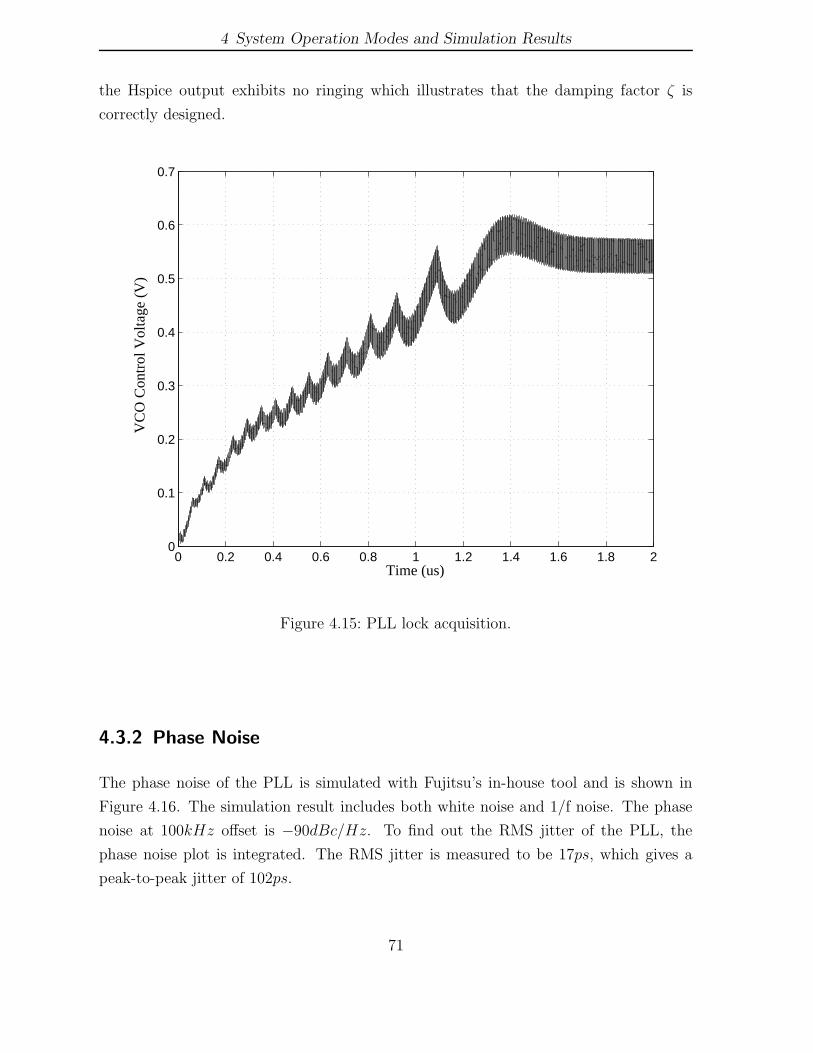
4 System Operation Modes and Simulation Results
the Hspice output exhibits no ringing which illustrates that the damping factor ζ is
correctly designed.
0 0.2 0.4 0.6 0.8 1 1.2 1.4 1.6 1.8 20
0.1
0.2
0.3
0.4
0.5
0.6
0.7
Time (us)
VC
O C
ontr
ol V
olta
ge (
V)
Figure 4.15: PLL lock acquisition.
4.3.2 Phase Noise
The phase noise of the PLL is simulated with Fujitsu’s in-house tool and is shown in
Figure 4.16. The simulation result includes both white noise and 1/f noise. The phase
noise at 100kHz offset is −90dBc/Hz. To find out the RMS jitter of the PLL, the
phase noise plot is integrated. The RMS jitter is measured to be 17ps, which gives a
peak-to-peak jitter of 102ps.
71
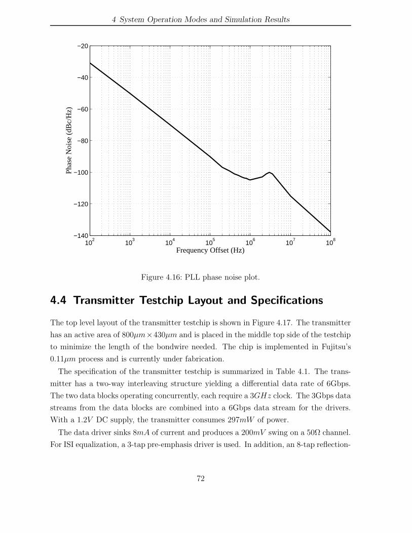
4 System Operation Modes and Simulation Results
102
103
104
105
106
107
108
−140
−120
−100
−80
−60
−40
−20
Frequency Offset (Hz)
Phas
e N
oise
(dB
c/H
z)
Figure 4.16: PLL phase noise plot.
4.4 Transmitter Testchip Layout and Specifications
The top level layout of the transmitter testchip is shown in Figure 4.17. The transmitter
has an active area of 800µm×430µm and is placed in the middle top side of the testchip
to minimize the length of the bondwire needed. The chip is implemented in Fujitsu’s
0.11µm process and is currently under fabrication.
The specification of the transmitter testchip is summarized in Table 4.1. The trans-
mitter has a two-way interleaving structure yielding a differential data rate of 6Gbps.
The two data blocks operating concurrently, each require a 3GHz clock. The 3Gbps data
streams from the data blocks are combined into a 6Gbps data stream for the drivers.
With a 1.2V DC supply, the transmitter consumes 297mW of power.
The data driver sinks 8mA of current and produces a 200mV swing on a 50Ω channel.
For ISI equalization, a 3-tap pre-emphasis driver is used. In addition, an 8-tap reflection-
72

4 System Operation Modes and Simulation Results
Figure 4.17: Testchip layout.
cancellation driver removes the signal reflections that are caused by channel impedance
discontinuities. The 8 continuous taps can be delayed from 0 to 126 UIs to match the
timing of the reflections. The ISI and reflection-cancellation drivers use similar driver
implementations as the data driver. There is a 6-bit control for the current source in
each tap, which can sink a maximum of 8mA.
The chip has an integrated 3GHz PLL to provide the clock for the transmitter.
The PLL requires an external reference clock between the range of 78.125MHz and
118.75MHz to generate an output clock frequency between 2.5GHz and 3.8GHz. The
testchip also supports an external clock to bypass the PLL clock. It is estimated that
the highest input frequency for the bypass clock is 200MHz.
4.5 Summary
This chapter presents the transmitter operation modes and the transmitter simulation
result. There are three operation modes for the transmitter: the scan-in mode, the cal-
ibration mode, and the data transmission mode. Scan-in mode allows the parameters
73

4 System Operation Modes and Simulation Results
Table 4.1: Transmitter testchip specifications.
Name Symbol Value Units NotesMin Typ Max
Technology 0.11 µmPower Supply 1.14 1.20 1.26 Volts
Reference Clock Frequency fref 78.125 100 118.75 MHzPLL Clock Frequency fclk 2.5 3 3.8 GHz
Data Rate 6 GbpsSignal Swing Vsw 200 mVPre-emphasis Vpreemph -200 200 mV 7-bit
Reflection Cancellation Vcancel -200 200 mV 7-bitPower Consumption P 297 mW
Layout Size 800 × 300 µm2
to be scanned into the scan-chain of the transmitter. The calibration mode obtains the
channel characteristics and allows the adjustment of the pre-emphasis and reflection-
cancellation drivers. The data transmission mode sends the transmitted data to the
channel. The simulation result from Hsim shows that the mini-JTAG controller is able
to start the scan-in process by enabling the scan-clock at the correct FSM state. Hspice
simulation results illustrate that improvments are made on the received signal eye di-
agrams by using the ISI and reflection-cancellation scheme. Finally, Hspice simulation
results show that the PLL is functional and is able to obtain phase locking during oper-
ation.
74

5 Conclusions
5.1 Summary
This thesis presented the design and implementation of a 6Gbps transmitter with ISI
and reflection cancellation. The transmitter can be divided into three main sections: the
transmitter digital block, the transmitter front-end and the PLL block. The transmitter
has a 2-way interleaving architecture, in which two half-rate data streams are combined
into one. The transmitter digital block provides the two half-rate data streams from
the 231 − 1 PRBS generator or the 128-bit user-defined data sequence. The transmitted
data is retimed and, if necessary, inverted before passed to the transmitter front-end for
transmission.
The transmitter front-end includes the high-speed data multiplexors, the data driver,
the pre-emphasis drivers, the reflection-cancellation drivers, the bias circuits, and the
termination resistors. The data multiplexors merge the two 3Gbps data streams from
the transmitter digital block into a 6Gbps data stream. The data driver then sends out
the combined data stream onto the channel. The ISI and reflection-cancellation drivers
use the delayed version of the transmitted data to cancel the ISI and reflections on the
channel.
ISI is cancelled by a 3-tap pre-emphasis driver in the transmitter. By adjusting the
6-bit digital control for each of the three pre-emphasis drivers, up to three UI of ISI
can be cancelled. Reflections are cancelled by an 8-tap reflection canceller that is also
implemented in the transmitter. The 6-bit variable delay block is used to delay the
cancellation signals to match the timing of the reflections. A maximum delay of 126UI,
with 1UI resolution, is possible from the variable delay block. The amplitude of the taps
can be individually adjusted to match the shape of the reflections. For the reflections
that are not located in the middle of the unit interval, the cancellation signals are
adjusted such that the reflections located at the interval boundaries are reduced as
much as possible, while emphasizing on zeroing the reflections in the middle of the unit
75

5 Conclusions
intervals.
The 3GHz PLL is used as a clock generator for the transmitter. The PLL uses an LC-
VCO as the oscillator, which has a tuning range between 2.5GHz and 3.8GHz. There
is an optional bypass clock to serve as a backup if the PLL malfunctions.
A testchip of the transmitter is implemented with the Fujitsu’s 0.11µm CMOS process
Extensive post-layout simulation is done on the transmitter to verify its functionality.
Simulation shows that improvments are made on the received signal eye diagram when
reflections and ISI are cancelled. The PLL has an acquistion time of less than 2us. In
addition, the phase noise at 10kHz offset is −90dBc/Hz, and it has an RMS jitter of
17ps.
5.2 Contributions
The transmitter described in the thesis is designed for chip-to-chip signaling applications.
The transmitter is capable of transmitting data at 6Gbps. It has a 3-tap pre-emphasis
driver for ISI equalization and an 8-tap reflection canceller for canceling signal reflections
in the channel.
A testchip of the transmitter is implemented in Fujitsu’s 0.11µm CMOS process,
and has been submitted for fabrication. Simulation results including severe impedance
mismatch and inductive reflections verify the testchip functionality at 6Gbps.
5.3 Future Work
There are four main areas in the transmitter design that can be considered for fur-
ture work: the time resolution of the reflection-cancellation block, the flexibility of the
reflection-cancellation taps, the automatic adjustment of the cancellation parameters,
and the power consumption of the transmitter.
The reflection-cancellation block is designed to have a timing resolution of one UI. This
is often inadequate in removing complicated reflections that are generated by reactive
loads. The current implementation of the reflection canceller is only capable of zeroing
the reflection in the middle of the unit interval. To get better quality of reflection
cancellation and a cleaner eye diagram, it is desirable to have a higher time resolution
in the reflection canceller. The timing of each reflection-cancellation tap should have
76

5 Conclusions
a resolution of at least half of a unit interval so that reflections located in the interval
boundaries are also cancelled.
Reflections often occur at multiple locations in the channel and they can be far apart
from each other. The reflection canceller in this transmitter is limited to have only
eight continuous taps. Thus, the reflection canceller cannot cancel multiple reflections
that are separated by more than eight UIs. A more flexible tap assignment should be
implemented such that the reflection canceller can cover a wider cancellation range.
The delay of the reflection-cancellation signals and the amount of compensation for
each tap are parameters that require manual adjustment. This is inadequate for pro-
duction chips. A receiver should be designed with a ”back-channel” to send channel
characteristics back to the transmitter so that these parameters can be automatically
adjusted. The back-channel does not have to be a high-speed link since the operating
environment of backplane systems changes slowly after operation. In the transmitter,
circuits should be designed to take the information from the receiver and adjust the
parameters accordingly.
The power consumption of the transmitter can be reduced by disabling the flip-flops
that are not in the delay path of the variable delay block. By disabling the clock signals
that drive these flip-flops, unnecessary switching activity is eliminated resulting in power
saving.
77

References
[AM00] P. Andreani and S. Mattisson. On the use of MOS varactors in RF VCO’s.JSSC, 35(6):905–910, June 2000.
[Buc03] A. Buchwald. Basics of serial backplane transceivers. ISSCC presentation,February 2003.
[DP97] W. J. Dally and J. Poulton. Transmitter equalization for 4-Gbps signaling.IEEE Micro, page 48, 1997.
[FMWK97] A. Fiedler, R. Mactaggart, J. Welch, and S. Krshnan. A 1.0625 Gbpstransceiver with 2x-oversampling and transmit signal pre-emphasis. IEEE
International Solids-State Circuits Conference, Digest of Technical Papers,pages 238–239, 1997.
[HHM00] S. H. Hall, G. W. Hall, and J. A. McCall. High-Speed Digital System Design,
A Handbook of Interconnect Theory and Design Practices. John Wiley andSons, 2000.
[IEE93] IEEE. IEEE standard test access port and boundary-scan architecture.IEEE Standards, October 1993.
[JM97] D. Johns and K. Martins. Analog Integrated Circuit Design. John Wileyand Sons, 1997.
[KFM02] Y. Kudoh, M. Fukaishi, and M. Mizuno. A 0.13-um CMOS 5-Gb/s10-meter 28AWG cable transceiver with no-feedback-loop continue-timepost-equalizer. Symposium On VLSI Circuits Digest of Technical Papers,page 64, 2002.
[LWJ03] C-H Lin, C-H Wang, and S-J. Jou. 5Gbps serial link transmitter withpre-emphasis. IEEE, page 795, 2003.
[NSO99] B. Nikolic, V. Stojanovic, and V. G. Oklondzja. Sense amplifier-based flip-flop. IEEE International Solid-State Circuits Conference, page 282, 1999.
[Rab96] J. M. Rabaey. Digital Integrated Circuits - A Design Perspective. PrenticeHall, Inc., 1996.
[Raz01] B. Razavi. Design of Analog CMOS Integrated Circuits. McGraw-Hill In-ternational Edition, 2001.
78

References
[Son96] B-S. Song. NRZ timing recovery technique for band limited channels. IEEE
International Solid-State Circuits Conference, pages 194–195, 1996.
[SR01] J. Savoj and B. Razavi. A 10Gb/s CMOS clock and data recovery circuitwith frequency detection. IEEE International Solid-State Circuits Confer-
ence, page 78, 2001.
[TTM+03] H. Takauchi, H. Tamura, S. Matsubara, M. Kibune, Y. Doi, T. Chiba,H. Anbutsu, H. Yamaguchi, T. Mori, M. Takatsu, K. Gotoh, T. Sakai,and T. Yamamura. A CMOS multi-channel 10Gb/s transceiver. IEEE
International Solid-State Circuits Conference, page 72, 2003.
[ZWS+03] J. Zerbe, C. Werner, V. Stojanovic, F. Chen, J. Wei, D. Kim G.Tsang,W. Stonecypher, T. Thrush A. Ho, R. Kollipara, G-J. Yeh, M. Horowitz, andK. Donnelly. Equalization and clock recovery for a 2.5-10Gb/s 2-PAM/4-PAM backplane transceiver cell. IEEE International Solid-State Circuits
Conference, page 80, 2003.
79