Embed Size (px)
Citation preview
A 5nW Wake-Up Receiver With Better Than-63dBm Sensitivity via an Active
Pseudo-Differential Envelope DetectorPatrick P. Mercier, Po-Han Peter Wang, Haowei Jiang, Li Gao, Pinar Sen,
Young-Han Kim, Gabriel M. Rebeiz, and Drew A. HallElectrical and Computer EngineeringUniversity of California - San Diego
La Jolla, CA 92093Email: [email protected], [email protected]
Abstract—A 402-405 MHz MICS-band wake-up receiver ispresented that achieves −63.8 dBm sensitivity at 4.5 nW. Highsensitivity at 400 MHz is accomplished via an 18.5 dB passivevoltage gain transformer filter loaded by a high input impedance(Rin > 30 kΩ), high scaling factor (kED > 300), 1.8 nWcurrent re-use pseudo-balun envelope detector, while low poweris achieved by operating all active circuits, including the re-generative comparator, baseband correlator, and temperaturecompensated relaxation oscillator in sub-threshold with a single0.4 V supply. The chip is fabricated using 0.18 µm CMOS SOIprocess and achieves the highest figure of merit of all directenvelope detection-based wake-up receivers operating above 400MHz.
Keywords—LPWAN; wake-up receiver; low power; wireless
I. INTRODUCTION
Wake-up receivers (WuRXs), used to continuously moni-tor the RF environment for infrequent event-driven wake-upsignals, can replace the need for energy-expensive synchro-nization routines frequently required in conventional radionetworks. WuRXs at nW power levels have been reported[1]–[3], however with moderate sensitivity. When used in lowaverage-throughput applications (e.g., wearable temperaturesensors or environmental monitors), wake-up latency, andtherefore data rate, can be relaxed. Prior work has exploitedsuch requirements to design low-bandwidth, and therefore low-noise, on-off keying (OOK) WuRXs that, along with a passiveRF gain transformer filter, achieved excellent sensitivity atnW power levels [4]. However, this prior work was limitedto 113.5 MHz, largely because of the low input impedance ofthe envelope detector (ED). While a low carrier frequency maybe suitable for some applications, such as unattended groundsensor networks, it is not practical for many wearable and IoTapplications. To enable operation at higher frequencies withoutsignificantly compromising sensitivity or power consumption,this paper presents the design of a WuRX featuring an activepseudo-balun ED. This new ED has higher input resistance,
Approved for public release: distribution unlimited.
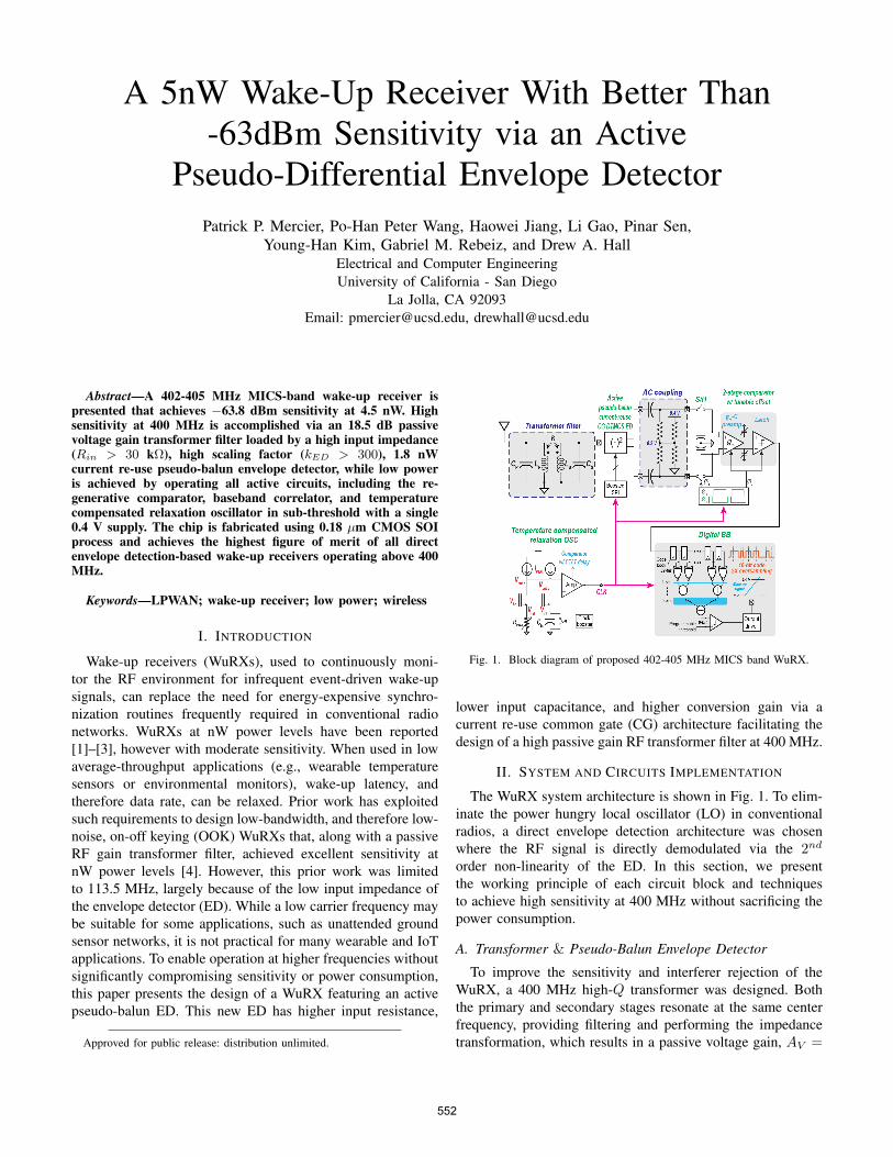
Fig. 1. Block diagram of proposed 402-405 MHz MICS band WuRX.
lower input capacitance, and higher conversion gain via acurrent re-use common gate (CG) architecture facilitating thedesign of a high passive gain RF transformer filter at 400 MHz.
II. SYSTEM AND CIRCUITS IMPLEMENTATION
The WuRX system architecture is shown in Fig. 1. To elim-inate the power hungry local oscillator (LO) in conventionalradios, a direct envelope detection architecture was chosenwhere the RF signal is directly demodulated via the 2nd
order non-linearity of the ED. In this section, we presentthe working principle of each circuit block and techniquesto achieve high sensitivity at 400 MHz without sacrificing thepower consumption.
A. Transformer & Pseudo-Balun Envelope Detector
To improve the sensitivity and interferer rejection of theWuRX, a 400 MHz high-Q transformer was designed. Boththe primary and secondary stages resonate at the same centerfrequency, providing filtering and performing the impedancetransformation, which results in a passive voltage gain, AV =
552
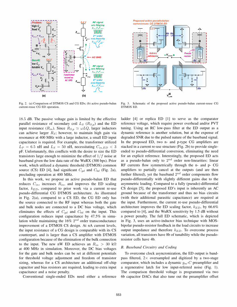
Fig. 2. (a) Comparison of DTMOS CS and CG EDs; (b) active pseudo-baluncurrent-reuse CG ED operation.
18.5 dB. The passive voltage gain is limited by the effectiveparallel resistance of secondary coil LS (RS,p) and the EDinput resistance (Rin). Since RS,p ' ωLQ, larger inductorscan achieve larger RS ; however, to maintain high gain viaresonance at 400 MHz with a large inductor, a small ED inputcapacitance is required. For example, the transformer utilizedLP = 6.5 nH and LS = 50 nH, necessitating Cin,ED < 3pF. Unfortunately, this conflicts with the desire to size the EDtransistors large enough to minimize the effect of 1/f noise atbaseband given the low data rate of the WuRX (300 bps). Priorwork, which utilized a dynamic threshold (DTMOS) commonsource (CS) ED [4], had significant Cgd and Cbd (Fig. 2a),precluding operation at 400 MHz.
In this work, we propose an active pseudo-balun ED thatreduces Cin, increases Rin, and improves the ED scalingfactor, kED, compared to prior work via a current re-usepseudo-differential CG DTMOS architecture. As illustratedin Fig. 2(a), compared to a CS ED, the CG ED only hasthe source connected to the RF input whereas both the gateand bulk nodes are connected to a DC bias voltage, whicheliminates the effects of Cgd and Cbd on the input. Thisconfiguration reduces input capacitance by 47.5% in simu-lation while maintaining the 16% 2nd order transconductanceimprovement of a DTMOS CS design. At nA current levels,the input resistance of a CG design is comparable with its CScounterpart, and is larger than a CS amplifier with DTMOSconfiguration because of the elimination of the bulk connectionto the input. The new nW ED achieves an Rin > 30 kΩat 400 MHz in simulation. Moreover, the DC bias voltagesfor the gate and bulk nodes can be set at different potentialsfor threshold voltage adjustment and freedom of transistorsizing, whereas for a CS architecture an additional off-chipcapacitor and bias resistors are required, leading to extra inputcapacitance and a noise penalty.
Conventional single-ended EDs need either a reference
Fig. 3. Schematic of the proposed active pseudo-balun current-reuse CGDTMOS ED.
ladder [4] or replica ED [1] to serve as the comparatorreference voltage, which require power overhead and/or PVTtuning. Using an RC low-pass filter at the ED output as adynamic reference is another solution, but at the expense ofdegraded SNR due to the pulsed nature of the baseband signal.In the proposed ED, two n- and p-type CG amplifiers arestacked in a current re-use structure (Fig. 2b) to provide single-ended to pseudo-differential conversion, eliminating the needfor an explicit reference. Interestingly, the proposed ED actsas a pseudo-balun only to 2nd order non-linearities: linearRF currents flow symmetrically through the n- and p- CGamplifiers to partially cancel at the outputs (and are thenfurther filtered), yet the baseband 2nd order components flowpseudo-differentially with slightly different gains due to theasymmetric loading. Compared to a fully (pseudo)-differentialCS design [5], the proposed ED’s input is inherently an ACground because of the transformer and thus no bias circuits(with their additional parasitic capacitance) are required atthe input. Furthermore, the current re-use pseudo-differentialarchitecture improves the ED scaling factor, kED, by 66.6%compared to [4], and the WuRX sensitivity by 1.5 dB withouta power penalty. The full ED schematic, which is depictedin Fig. 3, uses an active-inductor bias technique with MOS-bipolar pseudo-resistor feedback in the load circuits to increaseoutput impedance and therefore kED. To overcome processvariation, all transistors have 8b of tunability while the pseudo-resistor cells have 4b.
B. Baseband Circuitry and Coding
To overcome clock asyncronization, the ED output is band-pass filtered, 2× oversampled and digitized by a two-stagecomparator, which includes a dynamic gm-C preamplifier anda regenerative latch for low input-referred noise (Fig. 1).The comparison threshold voltage is programmed via two6b capacitor DACs that also tune out the preamplifier offset
553
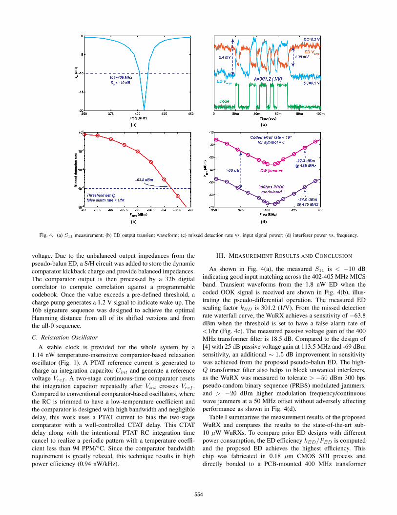
Fig. 4. (a) S11 measurement; (b) ED output transient waveform; (c) missed detection rate vs. input signal power; (d) interferer power vs. frequency.
voltage. Due to the unbalanced output impedances from thepseudo-balun ED, a S/H circuit was added to store the dynamiccomparator kickback charge and provide balanced impedances.The comparator output is then processed by a 32b digitalcorrelator to compute correlation against a programmablecodebook. Once the value exceeds a pre-defined threshold, acharge pump generates a 1.2 V signal to indicate wake-up. The16b signature sequence was designed to achieve the optimalHamming distance from all of its shifted versions and fromthe all-0 sequence.
C. Relaxation Oscillator
A stable clock is provided for the whole system by a1.14 nW temperature-insensitive comparator-based relaxationoscillator (Fig. 1). A PTAT reference current is generated tocharge an integration capacitor Cint and generate a referencevoltage Vref . A two-stage continuous-time comparator resetsthe integration capacitor repeatedly after Vint crosses Vref .Compared to conventional comparator-based oscillators, wherethe RC is trimmed to have a low-temperature coefficient andthe comparator is designed with high bandwidth and negligibledelay, this work uses a PTAT current to bias the two-stagecomparator with a well-controlled CTAT delay. This CTATdelay along with the intentional PTAT RC integration timecancel to realize a periodic pattern with a temperature coeffi-cient less than 94 PPM/C. Since the comparator bandwidthrequirement is greatly relaxed, this technique results in highpower efficiency (0.94 nW/kHz).
III. MEASUREMENT RESULTS AND CONCLUSION
As shown in Fig. 4(a), the measured S11 is < −10 dBindicating good input matching across the 402-405 MHz MICSband. Transient waveforms from the 1.8 nW ED when thecoded OOK signal is received are shown in Fig. 4(b), illus-trating the pseudo-differential operation. The measured EDscaling factor kED is 301.2 (1/V). From the missed detectionrate waterfall curve, the WuRX achieves a sensitivity of −63.8dBm when the threshold is set to have a false alarm rate of<1/hr (Fig. 4c). The measured passive voltage gain of the 400MHz transformer filter is 18.5 dB. Compared to the design of[4] with 25 dB passive voltage gain at 113.5 MHz and -69 dBmsensitivity, an additional ∼ 1.5 dB improvement in sensitivitywas achieved from the proposed pseudo-balun ED. The high-Q transformer filter also helps to block unwanted interferers,as the WuRX was measured to tolerate > −50 dBm 300 bpspseudo-random binary sequence (PRBS) modulated jammers,and > −20 dBm higher modulation frequency/continuouswave jammers at a 50 MHz offset without adversely affectingperformance as shown in Fig. 4(d).
Table I summarizes the measurement results of the proposedWuRX and compares the results to the state-of-the-art sub-10 µW WuRXs. To compare prior ED designs with differentpower consumption, the ED efficiency kED/PED is computedand the proposed ED achieves the highest efficiency. Thischip was fabricated in 0.18 µm CMOS SOI process anddirectly bonded to a PCB-mounted 400 MHz transformer
554
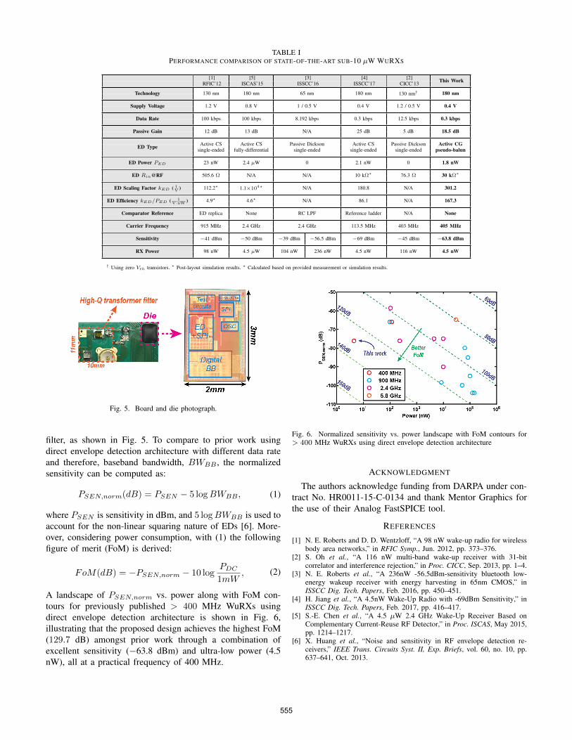
TABLE IPERFORMANCE COMPARISON OF STATE-OF-THE-ART SUB-10 µW WURXS
[1] [5] [3] [4] [2]RFIC’12 ISCAS’15 ISSCC’16 ISSCC’17 CICC’13 This Work
130 nm 180 nm 65 nm 180 nm 130 nm† 180 nmTechnology
1.2 V 0.8 V 1 / 0.5 V 0.4 V 1.2 / 0.5 V 0.4 VSupply Voltage
100 kbps 100 kbps 8.192 kbps 0.3 kbps 12.5 kbps 0.3 kbpsData Rate
12 dB 13 dB N/A 25 dB 5 dB 18.5 dBPassive Gain
Active CS Active CS Passive Dickson Active CS Passive Dickson Active CGsingle-ended fully-differential single-ended single-ended single-ended pseudo-balunED Type
23 nW 2.4 µW 0 2.1 nW 0 1.8 nWED Power PED
505.6 Ω N/A N/A 10 kΩ∗ 76.3 Ω 30 kΩ∗ED Rin@RF
112.2? 1.1×10⁴? N/A 180.8 N/A 301.2ED Scaling Factor kED ( 1V )
4.9? 4.6? N/A 86.1 N/A 167.3ED Efficiency kED/PED ( 1V·nW )
ED replica None RC LPF Reference ladder N/A NoneComparator Reference
915 MHz 2.4 GHz 2.4 GHz 113.5 MHz 403 MHz 405 MHzCarrier Frequency
−41 dBm −50 dBm −39 dBm −56.5 dBm −69 dBm −45 dBm −63.8 dBmSensitivity
98 nW 4.5 µW 104 nW 236 nW 4.5 nW 116 nW 4.5 nWRX Power
† Using zero Vth transistors. ∗ Post-layout simulation results. ? Calculated based on provided measurement or simulation results.
Fig. 5. Board and die photograph.
filter, as shown in Fig. 5. To compare to prior work usingdirect envelope detection architecture with different data rateand therefore, baseband bandwidth, BWBB , the normalizedsensitivity can be computed as:
PSEN,norm(dB) = PSEN − 5 logBWBB , (1)
where PSEN is sensitivity in dBm, and 5 logBWBB is used toaccount for the non-linear squaring nature of EDs [6]. More-over, considering power consumption, with (1) the followingfigure of merit (FoM) is derived:
FoM(dB) = −PSEN,norm − 10 logPDC1mW
, (2)
A landscape of PSEN,norm vs. power along with FoM con-tours for previously published > 400 MHz WuRXs usingdirect envelope detection architecture is shown in Fig. 6,illustrating that the proposed design achieves the highest FoM(129.7 dB) amongst prior work through a combination ofexcellent sensitivity (−63.8 dBm) and ultra-low power (4.5nW), all at a practical frequency of 400 MHz.
Fig. 6. Normalized sensitivity vs. power landscape with FoM contours for> 400 MHz WuRXs using direct envelope detection architecture
ACKNOWLEDGMENT
The authors acknowledge funding from DARPA under con-tract No. HR0011-15-C-0134 and thank Mentor Graphics forthe use of their Analog FastSPICE tool.
REFERENCES
[1] N. E. Roberts and D. D. Wentzloff, “A 98 nW wake-up radio for wirelessbody area networks,” in RFIC Symp., Jun. 2012, pp. 373–376.
[2] S. Oh et al., “A 116 nW multi-band wake-up receiver with 31-bitcorrelator and interference rejection,” in Proc. CICC, Sep. 2013, pp. 1–4.
[3] N. E. Roberts et al., “A 236nW -56.5dBm-sensitivity bluetooth low-energy wakeup receiver with energy harvesting in 65nm CMOS,” inISSCC Dig. Tech. Papers, Feb. 2016, pp. 450–451.
[4] H. Jiang et al., “A 4.5nW Wake-Up Radio with -69dBm Sensitivity,” inISSCC Dig. Tech. Papers, Feb. 2017, pp. 416–417.
[5] S.-E. Chen et al., “A 4.5 µW 2.4 GHz Wake-Up Receiver Based onComplementary Current-Reuse RF Detector,” in Proc. ISCAS, May 2015,pp. 1214–1217.
[6] X. Huang et al., “Noise and sensitivity in RF envelope detection re-ceivers,” IEEE Trans. Circuits Syst. II, Exp. Briefs, vol. 60, no. 10, pp.637–641, Oct. 2013.
555