Embed Size (px)
Citation preview
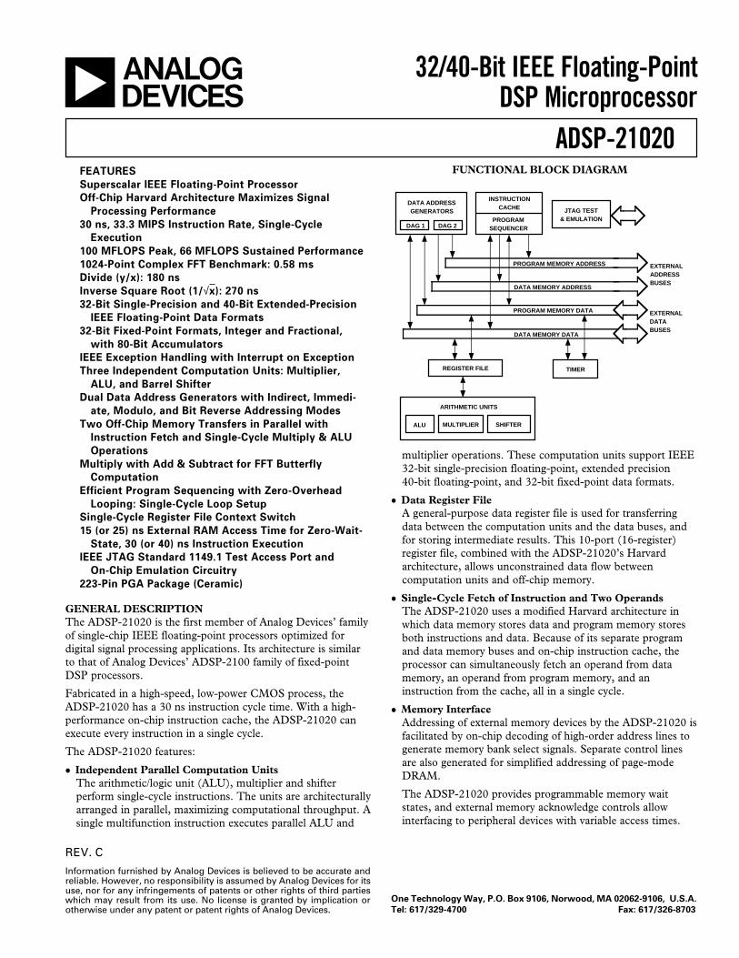
FUNCTIONAL BLOCK DIAGRAM
EXTERNALADDRESSBUSES
PROGRAMSEQUENCER
EXTERNALDATABUSES
DATA ADDRESSGENERATORS
DAG 1 DAG 2
PROGRAM MEMORY ADDRESS
PROGRAM MEMORY DATA
DATA MEMORY DATA
DATA MEMORY ADDRESS
INSTRUCTIONCACHE
ARITHMETIC UNITS
SHIFTERMULTIPLIERALU
REGISTER FILE TIMER
JTAG TEST& EMULATION
REV. C
Information furnished by Analog Devices is believed to be accurate andreliable. However, no responsibility is assumed by Analog Devices for itsuse, nor for any infringements of patents or other rights of third partieswhich may result from its use. No license is granted by implication orotherwise under any patent or patent rights of Analog Devices.
a 32/40-Bit IEEE Floating-PointDSP Microprocessor
ADSP-21020
One Technology Way, P.O. Box 9106, Norwood, MA 02062-9106, U.S.A.
Tel: 617/329-4700 Fax: 617/326-8703
GENERAL DESCRIPTIONThe ADSP-21020 is the first member of Analog Devices’ familyof single-chip IEEE floating-point processors optimized fordigital signal processing applications. Its architecture is similarto that of Analog Devices’ ADSP-2100 family of fixed-pointDSP processors.
Fabricated in a high-speed, low-power CMOS process, theADSP-21020 has a 30 ns instruction cycle time. With a high-performance on-chip instruction cache, the ADSP-21020 canexecute every instruction in a single cycle.
The ADSP-21020 features:
• Independent Parallel Computation UnitsThe arithmetic/logic unit (ALU), multiplier and shifterperform single-cycle instructions. The units are architecturallyarranged in parallel, maximizing computational throughput. Asingle multifunction instruction executes parallel ALU and
FEATURES
Superscalar IEEE Floating-Point Processor
Off-Chip Harvard Architecture Maximizes Signal
Processing Performance
30 ns, 33.3 MIPS Instruction Rate, Single-Cycle
Execution
100 MFLOPS Peak, 66 MFLOPS Sustained Performance
1024-Point Complex FFT Benchmark: 0.58 ms
Divide (y/x): 180 ns
Inverse Square Root (1/√x): 270 ns
32-Bit Single-Precision and 40-Bit Extended-Precision
IEEE Floating-Point Data Formats
32-Bit Fixed-Point Formats, Integer and Fractional,
with 80-Bit Accumulators
IEEE Exception Handling with Interrupt on Exception
Three Independent Computation Units: Multiplier,
ALU, and Barrel Shifter
Dual Data Address Generators with Indirect, Immedi-
ate, Modulo, and Bit Reverse Addressing Modes
Two Off-Chip Memory Transfers in Parallel with
Instruction Fetch and Single-Cycle Multiply & ALU
Operations
Multiply with Add & Subtract for FFT Butterfly
Computation
Efficient Program Sequencing with Zero-Overhead
Looping: Single-Cycle Loop Setup
Single-Cycle Register File Context Switch
15 (or 25) ns External RAM Access Time for Zero-Wait-
State, 30 (or 40) ns Instruction Execution
IEEE JTAG Standard 1149.1 Test Access Port and
On-Chip Emulation Circuitry
223-Pin PGA Package (Ceramic)
multiplier operations. These computation units support IEEE32-bit single-precision floating-point, extended precision40-bit floating-point, and 32-bit fixed-point data formats.
• Data Register FileA general-purpose data register file is used for transferringdata between the computation units and the data buses, andfor storing intermediate results. This 10-port (16-register)register file, combined with the ADSP-21020’s Harvardarchitecture, allows unconstrained data flow betweencomputation units and off-chip memory.
• Single-Cycle Fetch of Instruction and Two OperandsThe ADSP-21020 uses a modified Harvard architecture inwhich data memory stores data and program memory storesboth instructions and data. Because of its separate programand data memory buses and on-chip instruction cache, theprocessor can simultaneously fetch an operand from datamemory, an operand from program memory, and aninstruction from the cache, all in a single cycle.
• Memory InterfaceAddressing of external memory devices by the ADSP-21020 isfacilitated by on-chip decoding of high-order address lines togenerate memory bank select signals. Separate control linesare also generated for simplified addressing of page-modeDRAM.
The ADSP-21020 provides programmable memory waitstates, and external memory acknowledge controls allowinterfacing to peripheral devices with variable access times.
ADSP-21020
REV. C–2–
• Instruction CacheThe ADSP-21020 includes a high performance instructioncache that enables three-bus operation for fetching aninstruction and two data values. The cache is selective—onlythe instructions whose fetches conflict with program memorydata accesses are cached. This allows full-speed executionof core, looped operations such as digital filter multiply-accumulates and FFT butterfly processing.
• Hardware Circular BuffersThe ADSP-21020 provides hardware to implement circularbuffers in memory, which are common in digital filters andFourier transform implementations. It handles addresspointer wraparound, reducing overhead (thereby increasingperformance) and simplifying implementation. Circularbuffers can start and end at any location.
• Flexible Instruction SetThe ADSP-21020’s 48-bit instruction word accommodates avariety of parallel operations, for concise programming. Forexample, the ADSP-21020 can conditionally execute amultiply, an add, a subtract and a branch in a singleinstruction.
DEVELOPMENT SYSTEMThe ADSP-21020 is supported with a complete set of softwareand hardware development tools. The ADSP-21000 FamilyDevelopment System includes development software, anevaluation board and an in-circuit emulator.
• AssemblerCreates relocatable, COFF (Common Object File Format)object files from ADSP-21xxx assembly source code. Itaccepts standard C preprocessor directives for conditionalassembly and macro processing. The algebraic syntax of theADSP-21xxx assembly language facilitates coding anddebugging of DSP algorithms.
• Linker/LibrarianThe Linker processes separately assembled object files andlibrary files to create a single executable program. It assignsmemory locations to code and to data in accordance with auser-defined architecture file that describes the memory andI/O configuration of the target system. The Librarian allowsyou to group frequently used object files into a single libraryfile that can be linked with your main program.
• SimulatorThe Simulator performs interactive, instruction-levelsimulation of ADSP-21xxx code within the hardwareconfiguration described by a system architecture file. It flagsillegal operations and supports full symbolic disassembly. Itprovides an easy-to-use, window oriented, graphical userinterface that is identical to the one used by the ADSP-21020EZ-ICE Emulator. Commands are accessed from pull-downmenus with a mouse.
• PROM SplitterFormats an executable file into files that can be used with anindustry-standard PROM programmer.
• C Compiler and Runtime LibraryThe C Compiler complies with ANSI specifications. It takesadvantage of the ADSP-21020’s high-level language architec-tural features and incorporates optimizing algorithms to speedup the execution of code. It includes an extensive runtimelibrary with over 100 standard and DSP-specific functions.
• C Source Level DebuggerA full-featured C source level debugger that works with thesimulator or EZ-ICE emulator to allow debugging ofassembler source, C source, or mixed assembler and C.
• Numerical C CompilerSupports ANSI Standard (X3J11.1) Numerical C as definedby the Numeric C Extensions Group. The compiler accepts Csource input containing Numerical C extensions for arrayselection, vector math operations, complex data types,circular pointers, and variably dimensioned arrays, andoutputs ADSP-21xxx assembly language source code.
• ADSP-21020 EZ-LAB® Evaluation BoardThe EZ-LAB Evaluation Board is a general-purpose, stand-alone ADSP-21020 system that includes 32K words ofprogram memory and 32K words of data memory as well asanalog I/O. A PC RS-232 download path enables the user todownload and run programs directly on the EZ-LAB. Inaddition, it may be used in conjunction with the EZ-ICEEmulator to provide a powerful software debug environment.
• ADSP-21020 EZ-ICE® EmulatorThis in-circuit emulator provides the system designer with aPC-based development environment that allows nonintrusiveaccess to the ADSP-21020’s internal registers through theprocessor’s 5-pin JTAG Test Access Port. This use of on-chipemulation circuitry enables reliable, full-speed performance inany target. The emulator uses the same graphical user inter-face as the ADSP-21020 Simulator, allowing an easy tran-sition from software to hardware debug. (See “Target SystemRequirements for Use of EZ-ICE Emulator” on page 27.)
ADDITIONAL INFORMATIONThis data sheet provides a general overview of ADSP-21020functionality. For additional information on the architecture andinstruction set of the processor, refer to the ADSP-21020 User’sManual. For development system and programming referenceinformation, refer to the ADSP-21000 Family DevelopmentSoftware Manuals and the ADSP-21020 Programmer’s QuickReference. Applications code listings and benchmarks for keyDSP algorithms are available on the DSP Applications BBS; call(617) 461-4258, 8 data bits, no parity, 1 stop bit, 300/1200/2400/9600 baud.
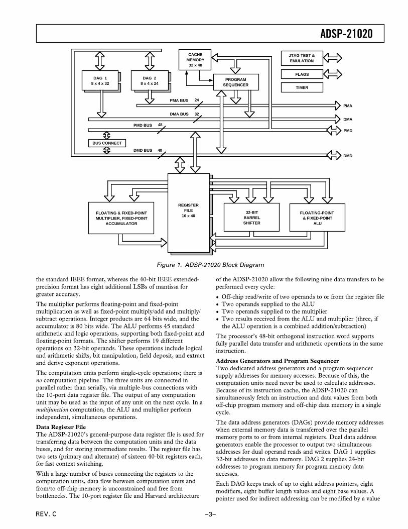
ARCHITECTURE OVERVIEWFigure 1 shows a block diagram of the ADSP-21020. Theprocessor features:
• Three Computation Units (ALU, Multiplier, and Shifter)with a Shared Data Register File
• Two Data Address Generators (DAG 1, DAG 2)• Program Sequencer with Instruction Cache• 32-Bit Timer• Memory Buses and Interface• JTAG Test Access Port and On-Chip Emulation Support
Computation UnitsThe ADSP-21020 contains three independent computationunits: an ALU, a multiplier with fixed-point accumulator, and ashifter. In order to meet a wide variety of processing needs, thecomputation units process data in three formats: 32-bitfixed-point, 32-bit floating-point and 40-bit floating-point. Thefloating-point operations are single-precision IEEE-compatible(IEEE Standard 754/854). The 32-bit floating-point format is
EZ-LAB and EZ-ICE are registered trademarks of Analog Devices, Inc.
ADSP-21020
REV. C –3–
the standard IEEE format, whereas the 40-bit IEEE extended-precision format has eight additional LSBs of mantissa forgreater accuracy.
The multiplier performs floating-point and fixed-pointmultiplication as well as fixed-point multiply/add and multiply/subtract operations. Integer products are 64 bits wide, and theaccumulator is 80 bits wide. The ALU performs 45 standardarithmetic and logic operations, supporting both fixed-point andfloating-point formats. The shifter performs 19 differentoperations on 32-bit operands. These operations include logicaland arithmetic shifts, bit manipulation, field deposit, and extractand derive exponent operations.
The computation units perform single-cycle operations; there isno computation pipeline. The three units are connected inparallel rather than serially, via multiple-bus connections withthe 10-port data register file. The output of any computationunit may be used as the input of any unit on the next cycle. In amultifunction computation, the ALU and multiplier performindependent, simultaneous operations.
Data Register FileThe ADSP-21020’s general-purpose data register file is used fortransferring data between the computation units and the databuses, and for storing intermediate results. The register file hastwo sets (primary and alternate) of sixteen 40-bit registers each,for fast context switching.
With a large number of buses connecting the registers to thecomputation units, data flow between computation units andfrom/to off-chip memory is unconstrained and free frombottlenecks. The 10-port register file and Harvard architecture
of the ADSP-21020 allow the following nine data transfers to beperformed every cycle:
• Off-chip read/write of two operands to or from the register file• Two operands supplied to the ALU• Two operands supplied to the multiplier• Two results received from the ALU and multiplier (three, if
the ALU operation is a combined addition/subtraction)
The processor’s 48-bit orthogonal instruction word supportsfully parallel data transfer and arithmetic operations in the sameinstruction.
Address Generators and Program SequencerTwo dedicated address generators and a program sequencersupply addresses for memory accesses. Because of this, thecomputation units need never be used to calculate addresses.Because of its instruction cache, the ADSP-21020 cansimultaneously fetch an instruction and data values from bothoff-chip program memory and off-chip data memory in a singlecycle.
The data address generators (DAGs) provide memory addresseswhen external memory data is transferred over the parallelmemory ports to or from internal registers. Dual data addressgenerators enable the processor to output two simultaneousaddresses for dual operand reads and writes. DAG 1 supplies32-bit addresses to data memory. DAG 2 supplies 24-bitaddresses to program memory for program memory dataaccesses.
Each DAG keeps track of up to eight address pointers, eightmodifiers, eight buffer length values and eight base values. Apointer used for indirect addressing can be modified by a value
DAG 28 x 4 x 24
DAG 18 x 4 x 32
CACHEMEMORY
32 x 48
PROGRAMSEQUENCER
PMD BUS
DMD BUS
24PMA BUS
PMD
DMD
PMA
32DMA BUSDMA
48
40
JTAG TEST &EMULATION
FLAGS
FLOATING & FIXED-POINTMULTIPLIER, FIXED-POINT
ACCUMULATOR
32-BITBARRELSHIFTER
FLOATING-POINT & FIXED-POINT
ALU
REGISTERFILE
16 x 40
BUS CONNECT
TIMER
Figure 1. ADSP-21020 Block Diagram
ADSP-21020
REV. C–4–
in a specified register, either before (premodify) or after(postmodify) the access. To implement automatic moduloaddressing for circular buffers, the ADSP-21020 provides bufferlength registers that can be associated with each pointer. Basevalues for pointers allow circular buffers to be placed at arbitrarylocations. Each DAG register has an alternate register that canbe activated for fast context switching.
The program sequencer supplies instruction addresses toprogram memory. It controls loop iterations and evaluatesconditional instructions. To execute looped code with zerooverhead, the ADSP-21020 maintains an internal loop counterand loop stack. No explicit jump or decrement instructions arerequired to maintain the loop.
The ADSP-21020 derives its high clock rate from pipelinedfetch, decode and execute cycles. Approximately 70% of themachine cycle is available for memory accesses; consequently,ADSP-21020 systems can be built using slower and thereforeless expensive memory chips.
Instruction CacheThe program sequencer includes a high performance, selectiveinstruction cache that enables three-bus operation for fetchingan instruction and two data values. This two-way, set-associativecache holds 32 instructions. The cache is selective—only theinstructions whose fetches conflict with program memory dataaccesses are cached, so the ADSP-21020 can perform a programmemory data access and can execute the corresponding instructionin the same cycle. The program sequencer fetches the instructionfrom the cache instead of from program memory, enabling theADSP-21020 to simultaneously access data in both programmemory and data memory.
Context SwitchingMany of the ADSP-21020’s registers have alternate register setsthat can be activated during interrupt servicing to facilitate a fastcontext switch. The data registers in the register file, DAGregisters and the multiplier result register all have alternate sets.Registers active at reset are called primary registers; the othersare called alternate registers. Bits in the MODE1 control registerdetermine which registers are active at any particular time.
The primary/alternate select bits for each half of the register file(top eight or bottom eight registers) are independent. Likewise,the top four and bottom four register sets in each DAG haveindependent primary/ alternate select bits. This scheme allowspassing of data between contexts.
InterruptsThe ADSP-21020 has four external hardware interrupts, nineinternally generated interrupts, and eight software interrupts.For the external interrupts and the internal timer interrupt, theADSP-21020 automatically stacks the arithmetic status andmode (MODE1) registers when servicing the interrupt, allowingfive nesting levels of fast service for these interrupts.
An interrupt can occur at any time while the ADSP-21020 isexecuting a program. Internal events that generate interruptsinclude arithmetic exceptions, which allow for fast trap handlingand recovery.
TimerThe programmable interval timer provides periodic interruptgeneration. When enabled, the timer decrements a 32-bit countregister every cycle. When this count register reaches zero, theADSP-21020 generates an interrupt and asserts its TIMEXP
output. The count register is automatically reloaded from a32-bit period register and the count resumes immediately.
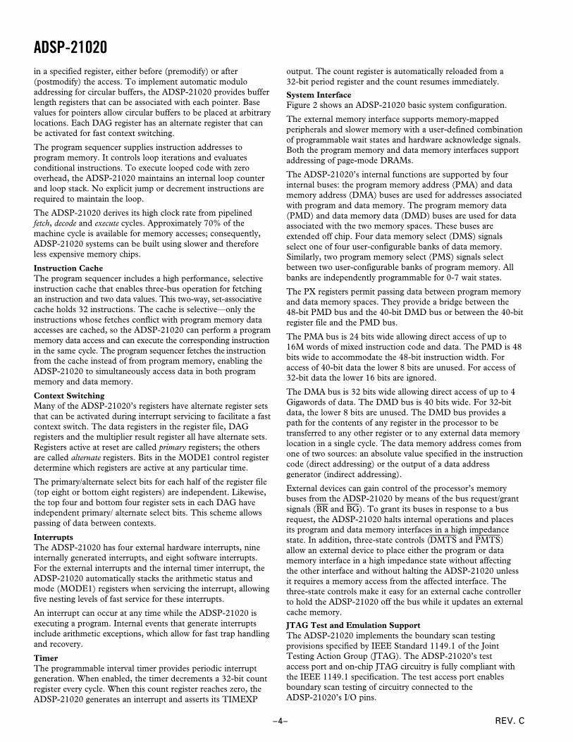
System InterfaceFigure 2 shows an ADSP-21020 basic system configuration.
The external memory interface supports memory-mappedperipherals and slower memory with a user-defined combinationof programmable wait states and hardware acknowledge signals.Both the program memory and data memory interfaces supportaddressing of page-mode DRAMs.
The ADSP-21020’s internal functions are supported by fourinternal buses: the program memory address (PMA) and datamemory address (DMA) buses are used for addresses associatedwith program and data memory. The program memory data(PMD) and data memory data (DMD) buses are used for dataassociated with the two memory spaces. These buses areextended off chip. Four data memory select (DMS) signalsselect one of four user-configurable banks of data memory.Similarly, two program memory select (PMS) signals selectbetween two user-configurable banks of program memory. Allbanks are independently programmable for 0-7 wait states.
The PX registers permit passing data between program memoryand data memory spaces. They provide a bridge between the48-bit PMD bus and the 40-bit DMD bus or between the 40-bitregister file and the PMD bus.
The PMA bus is 24 bits wide allowing direct access of up to16M words of mixed instruction code and data. The PMD is 48bits wide to accommodate the 48-bit instruction width. Foraccess of 40-bit data the lower 8 bits are unused. For access of32-bit data the lower 16 bits are ignored.
The DMA bus is 32 bits wide allowing direct access of up to 4Gigawords of data. The DMD bus is 40 bits wide. For 32-bitdata, the lower 8 bits are unused. The DMD bus provides apath for the contents of any register in the processor to betransferred to any other register or to any external data memorylocation in a single cycle. The data memory address comes fromone of two sources: an absolute value specified in the instructioncode (direct addressing) or the output of a data addressgenerator (indirect addressing).
External devices can gain control of the processor’s memorybuses from the ADSP-21020 by means of the bus request/grantsignals (BR and BG). To grant its buses in response to a busrequest, the ADSP-21020 halts internal operations and placesits program and data memory interfaces in a high impedancestate. In addition, three-state controls (DMTS and PMTS)allow an external device to place either the program or datamemory interface in a high impedance state without affectingthe other interface and without halting the ADSP-21020 unlessit requires a memory access from the affected interface. Thethree-state controls make it easy for an external cache controllerto hold the ADSP-21020 off the bus while it updates an externalcache memory.
JTAG Test and Emulation SupportThe ADSP-21020 implements the boundary scan testingprovisions specified by IEEE Standard 1149.1 of the JointTesting Action Group (JTAG). The ADSP-21020’s testaccess port and on-chip JTAG circuitry is fully compliant withthe IEEE 1149.1 specification. The test access port enablesboundary scan testing of circuitry connected to theADSP-21020’s I/O pins.
ADSP-21020
REV. C –5–
4
1×CLOCK
CLKIN
PMA
PMD
DMACK
DMA
DMD
ADSP-21010
24
48
32
32
2
PMACK
4
DMPAGEPMPAGE
FL
AG
3-0
JTA
G
54
RC
OM
P
TIM
EX
P
ADDR
DATA
PROGRAMMEMORY
SELECTS
OE
WE
PMS1-0
PMRD
PMWR
DMRD
DMWR
DMTS
DATAMEMORY
ACK
PERIPHERALS
ADDR
DATA
ADDR
DATA
SELECTS
SELECTS
OE
WE
OE
WE
BR
BG
RESET IRQ3-0
PMTS
DMS3-0
Figure 2. Basic System Configuration
The ADSP-21020 also implements on-chip emulation throughthe JTAG test access port. The processor’s eight sets of break-point range registers enable program execution at full speeduntil reaching a desired break-point address range. Theprocessor can then halt and allow reading/writing of all theprocessor’s internal registers and external memories through theJTAG port.
PIN DESCRIPTIONSThis section describes the pins of the ADSP-21020. Whengroups of pins are identified with subscripts, e.g. PMD47–0, thehighest numbered pin is the MSB (in this case, PMD47). Inputsidentified as synchronous (S) must meet timing requirementswith respect to CLKIN (or with respect to TCK for TMS, TDI,and TRST). Those that are asynchronous (A) can be assertedasynchronously to CLKIN.
O = Output; I = Input; S = Synchronous; A = Asynchronous;P = Power Supply; G = Ground.
PinName Type Function
PMA23–0 O Program Memory Address. The ADSP-21020outputs an address in program memory onthese pins.
PMD47–0 I/O Program Memory Data. The ADSP-21020inputs and outputs data and instructions onthese pins. 32-bit fixed-point data and 32-bitsingle-precision floating-point data is trans-ferred over bits 47-16 of the PMD bus.
PMS1–0 O Program Memory Select lines. These pins areasserted as chip selects for the correspondingbanks of program memory. Memory banksmust be defined in the memory controlregisters. These pins are decoded programmemory address lines and provide an earlyindication of a possible bus cycle.
PMRD O Program Memory Read strobe. This pin isasserted when the ADSP-21020 reads fromprogram memory.
PMWR O Program Memory Write strobe. This pin isasserted when the ADSP-21020 writes toprogram memory.
PMACK I/S Program Memory Acknowledge. An externaldevice deasserts this input to add wait statesto a memory access.
PinName Type Function
PMPAGE O Program Memory Page Boundary. TheADSP-21020 asserts this pin to signal that aprogram memory page boundary has beencrossed. Memory pages must be defined inthe memory control registers.
PMTS I/S Program Memory Three-State Control.PMTS places the program memory address,data, selects, and strobes in a high-impedance state. If PMTS is asserted whilea PM access is occurring, the processor willhalt and the memory access will not becompleted. PMACK must be asserted for atleast one cycle when PMTS is deasserted toallow any pending memory access to com-plete properly. PMTS should only beasserted (low) during an active memoryaccess cycle.
DMA31–0 O Data Memory Address. The ADSP-21020outputs an address in data memory on thesepins.
DMD39–0 I/O Data Memory Data. The ADSP-21020inputs and outputs data on these pins.32-bit fixed point data and 32-bitsingle-precision floating point data istransferred over bits 39-8 of the DMD bus.
DMS3–0 O Data Memory Select lines. These pins areasserted as chip selects for the correspon-ding banks of data memory. Memory banksmust be defined in the memory controlregisters. These pins are decoded datamemory address lines and provide an earlyindication of a possible bus cycle.
DMRD O Data Memory Read strobe. This pin isasserted when the ADSP-21020 reads fromdata memory.
DMWR O Data Memory Write strobe. This pin isasserted when the ADSP-21020 writes todata memory.
DMACK I/S Data Memory Acknowledge. An externaldevice deasserts this input to add wait statesto a memory access.
ADSP-21020
REV. C–6–
PinName Type Function
DMPAGE O Data Memory Page Boundary. The ADSP-21020 asserts this pin to signal that a datamemory page boundary has been crossed.Memory pages must be defined in thememory control registers.
DMTS I/S Data Memory Three-State Control. DMTSplaces the data memory address, data,selects, and strobes in a high-impedancestate. If DMTS is asserted while a DMaccess is occurring, the processor will haltand the memory access will not becompleted. DMACK must be asserted forat least one cycle when DMTS isdeasserted to allow any pending memoryaccess to complete properly. DMTS shouldonly be asserted (low) during an activememory access cycle.
CLKIIN I External clock input to the ADSP-21020.The instruction cycle rate is equal toCLKIN. CLKIN may not be halted,changed, or operated below the specifiedfrequency.
RESET I/A Sets the ADSP-21020 to a known state andbegins execution at the program memorylocation specified by the hardware resetvector (address). This input must beasserted (low) at power-up.
IRQ3–0 I/A Interrupt request lines; may be either edgetriggered or level-sensitive.
FLAG3–0 I/O/A External Flags. Each is configured viacontrol bits as either an input or output. Asan input, it can be tested as a condition. Asan output, it can be used to signal externalperipherals.
BR I/A Bus Request. Used by an external device torequest control of the memory interface.When BR is asserted, the processor haltsexecution after completion of the currentcycle, places all memory data, addresses,selects, and strobes in a high-impedancestate, and asserts BG. The processorcontinues normal operation when BR isreleased.
BG O Bus Grant. Acknowledges a bus request(BR), indicating that the external devicemay take control of the memory interface.BG is asserted (held low) until BR isreleased.
TIMEXP O Timer Expired. Asserted for four cycleswhen the value of TCOUNT isdecremented to zero.
RCOMP Compensation Resistor input. Controlscompensated output buffers. ConnectRCOMP through a 1.8 kΩ ±15% resistorto EVDD. Use of a capacitor (approxi-mately 100 pF), placed in parallel with the1.8 kΩ resistor is recommended.
EVDD P Power supply (for output drivers),nominally +5 V dc (10 pins).
EGND G Power supply return (for output drivers);(16 pins).
PinName Type Function
IVDD P Power supply (for internal circuitry),nominally +5 V dc (4 pins).
IGND G Power supply return (for internal circuitry); (7pins).
TCK I Test Clock. Provides an asynchronous clockfor JTAG boundary scan.
TMS I/S Test Mode Select. Used to control the teststate machine. TMS has a 20 kΩ internalpullup resistor.
TDI VS Test Data Input. Provides serial data for theboundary scan logic. TDI has a 20 kΩ internalpullup resistor.
TDO O Test Data Output. Serial scan output of theboundary scan path.
TRST I/A Test Reset. Resets the test state machine.TRST must be asserted (pulsed low) afterpower-up or held low for proper operation ofthe ADSP-21020. TRST has a 20 kΩ internalpullup resistor.
NC No Connect. No Connects are reserved pinsthat must be left open and unconnected.
INSTRUCTION SET SUMMARYThe ADSP-21020 instruction set provides a wide variety ofprogramming capabilities. Every instruction assembles into asingle word and can execute in a single processor cycle.Multifunction instructions enable simultaneous multiplier andALU operations, as well as computations executed in parallelwith data transfers. The addressing power of the ADSP-21020gives you flexibility in moving data both internally andexternally. The ADSP-21020 assembly language uses analgebraic syntax for ease of coding and readability.
The instruction types are grouped into four categories:Compute and Move or ModifyProgram Flow ControlImmediate MoveMiscellaneous
The instruction types are numbered; there are 22 types. Someinstructions have more than one syntactical form; for example,Instruction 4 has four distinct forms. The instruction numberitself has no bearing on programming, but corresponds to theopcode recognized by the ADSP-21020 device.
Because of the width and orthogonality of the instruction word,there are many possible instructions. For example, the ALUsupports 21 fixed-point operations and 24 floating-pointoperations; each of these operations can be the compute portionof an instruction.
The following pages provide an overview and summary of theADSP-21020 instruction set. For complete information, see theADSP-21020 User’s Manual. For additional reference informa-tion, see the ADSP-21020 Programmer’s Quick Reference.
This section also contains several reference tables for using theinstruction set.
• Table I describes the notation and abbreviations used.• Table II lists all condition and termination code mnemonics.• Table III lists all register mnemonics.• Tables IV through VII list the syntax for all compute
(ALU, multiplier, shifter or multifunction) operations.• Table VIII lists interrupts and their vector addresses.
ADSP-21020
REV. C –7–
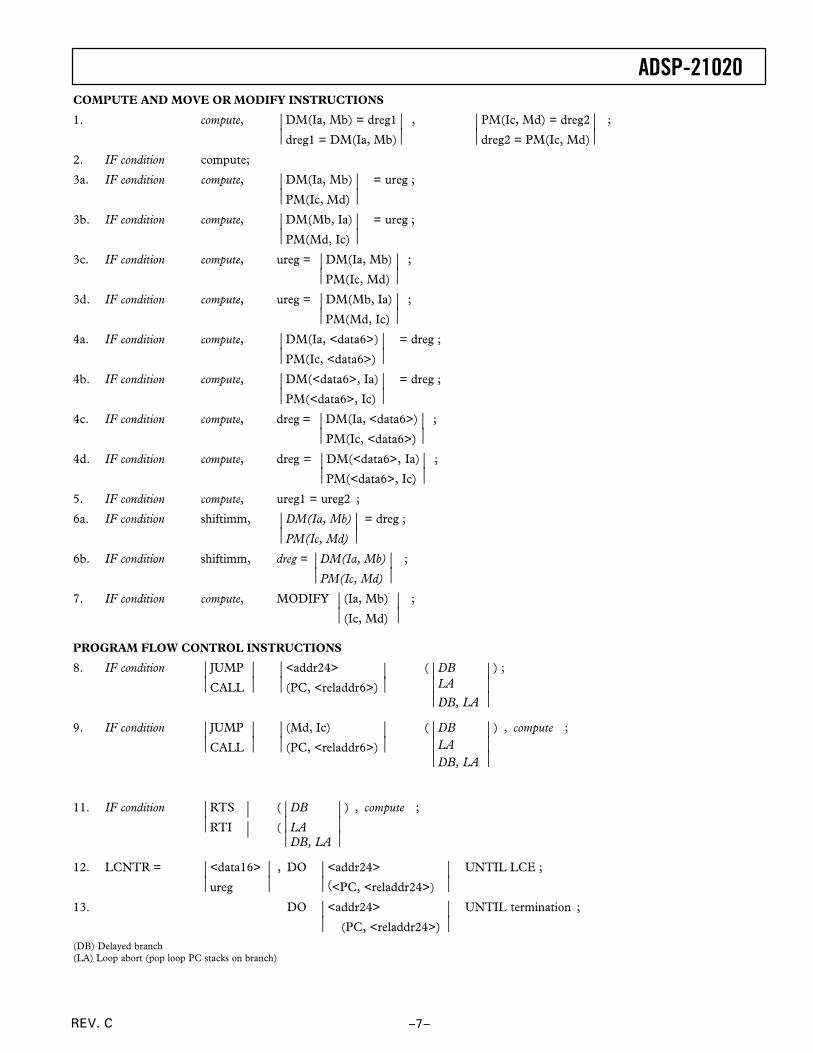
COMPUTE AND MOVE OR MODIFY INSTRUCTIONS
1. compute, |DM(Ia, Mb) = dreg1| , |PM(Ic, Md) = dreg2| ;|dreg1 = DM(Ia, Mb)| |dreg2 = PM(Ic, Md)|
2. IF condition compute;
3a. IF condition compute, |DM(Ia, Mb)| = ureg ;|PM(Ic, Md) |
3b. IF condition compute, |DM(Mb, Ia)| = ureg ;|PM(Md, Ic) |
3c. IF condition compute, ureg = |DM(Ia, Mb)| ;|PM(Ic, Md) |
3d. IF condition compute, ureg = |DM(Mb, Ia)| ;|PM(Md, Ic) |
4a. IF condition compute, |DM(Ia, <data6>)| = dreg ;|PM(Ic, <data6>) |
4b. IF condition compute, |DM(<data6>, Ia)| = dreg ;|PM(<data6>, Ic) |
4c. IF condition compute, dreg = |DM(Ia, <data6>)| ;|PM(Ic, <data6>) |
4d. IF condition compute, dreg = |DM(<data6>, Ia)| ;|PM(<data6>, Ic) |
5. IF condition compute, ureg1 = ureg2 ;
6a. IF condition shiftimm, |DM(Ia, Mb)| = dreg ;|PM(Ic, Md) |
6b. IF condition shiftimm, dreg = |DM(Ia, Mb)| ;|PM(Ic, Md) |
7. IF condition compute, MODIFY |(Ia, Mb) | ;
7. IF condition compute, MODIFY |(Ic, Md) |
PROGRAM FLOW CONTROL INSTRUCTIONS
8. IF condition |JUMP | |<addr24> | (|DB |) ;|CALL | |(PC, <reladdr6>)| (|LA, ||CALL| |(PC, <reladdr6>)| (
|DB, LA |
9. IF condition |JUMP | |(Md, Ic) | (|DB |) , compute ;|CALL | |(PC, <reladdr6>)| (|LA, ||CALL| |(PC, <reladdr6>)| (
|DB, LA |
11. IF condition |RTS | (|DB, |) , compute ;|RTI | (|LA, ||RTI | (
|DB, LA |
12. LCNTR = |<data16> | , DO |<addr24> | UNTIL LCE ;
12. LCNTR = |ureg | , DO |(<PC, <reladdr24>)( | UNTIL LCE ;
13. LCNTR = |<data16> | , DO |<addr24> | UNTIL termination ;
12. LCNTR = |ureg | , DO |(|(PC, <reladdr24>) |(DB) Delayed branch(LA) Loop abort (pop loop PC stacks on branch)
ADSP-21020
REV. C–8–
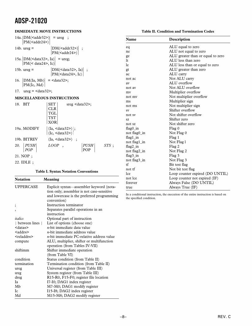
Table II. Condition and Termination Codes
Name Description
eq ALU equal to zerone ALU not equal to zeroge ALU greater than or equal to zerolt ALU less than zerole ALU less than or equal to zerogt ALU greater than zeroac ALU carrynot ac Not ALU carryav ALU overflownot av Not ALU overflowmv Multiplier overflownot mv Not multiplier overflowms Multiplier signnot ms Not multiplier signsv Shifter overflownot sv Not shifter overflowsz Shifter zeronot sz Not shifter zeroflag0_in Flag 0not flag0_in Not Flag 0flag1_in Flag 1not flag1_in Not Flag lflag2_in Flag 2not flag2_in Not Flag 2flag3_in Flag 3not flag3_in Not Flag 3tf Bit test flagnot tf Not bit test flaglce Loop counter expired (DO UNTIL)not lce Loop counter not expired (IF)forever Always False (DO UNTIL)true Always True (IF)
In a conditional instruction, the execution of the entire instruction is based onthe specified condition.
IMMEDIATE MOVE INSTRUCTIONS
14a. DM(<addr32>) = ureg ;PM(<addr24>)
14b. ureg = DM(<addr32>) ;PM(<addr24>)
15a. DM(<data32>, Ia) = ureg;PM(< data24>, Ic)
15b. ureg = DM(<data32>, Ia) ;PM(<data24>, Ic)
16. DM(Ia, Mb) = <data32>;PM(Ic, Md)
17. ureg = <data32>;
MISCELLANEOUS INSTRUCTIONS
18. BIT SET sreg <data32>;CLRTGLTSTXOR
19a. MODIFY (Ia, <data32>)|;(Ic, <data32>)|
19b. BITREV (Ia, <data32>) ;
20. |PUSH LOOP , PUSH STS ;|POP POP
21. NOP ;
22. IDLE ;
Table I. Syntax Notation Conventions
Notation Meaning
UPPERCASE Explicit syntax—assembler keyword (nota-tion only; assembler is not case-sensitiveand lowercase is the preferred programmingconvention)
; Instruction terminator, Separates parallel operations in an
instructionitalics Optional part of instruction| between lines | List of options (choose one)<datan> n-bit immediate data value<addrn> n-bit immediate address value<reladdrn> n-bit immediate PC-relative address valuecompute ALU, multiplier, shifter or multifunction
operation (from Tables IV-VII)shiftimm Shifter immediate operation
(from Table VI)condition Status condition (from Table II)termination Termination condition (from Table II)ureg Universal register (from Table III)sreg System register (from Table III)dreg R15-R0, F15-F0; register file locationIa I7-I0; DAG1 index registerMb M7-M0; DAG1 modify registerIc I15-I8; DAG2 index registerMd M15-M8; DAG2 modify register
ADSP-21020
REV. C –9–
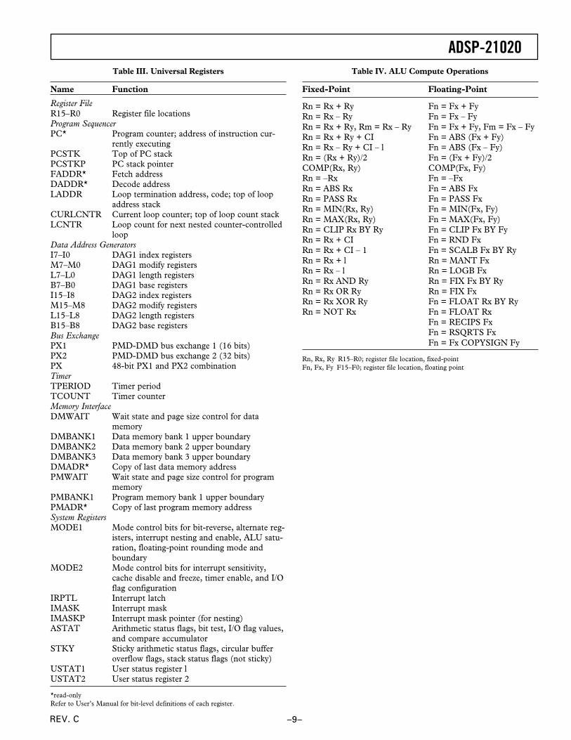
Table III. Universal Registers
Name Function
Register FileR15–R0 Register file locationsProgram SequencerPC* Program counter; address of instruction cur-
rently executingPCSTK Top of PC stackPCSTKP PC stack pointerFADDR* Fetch addressDADDR* Decode addressLADDR Loop termination address, code; top of loop
address stackCURLCNTR Current loop counter; top of loop count stackLCNTR Loop count for next nested counter-controlled
loopData Address GeneratorsI7–I0 DAG1 index registersM7–M0 DAG1 modify registersL7–L0 DAG1 length registersB7–B0 DAG1 base registersI15–I8 DAG2 index registersM15–M8 DAG2 modify registersL15–L8 DAG2 length registersB15–B8 DAG2 base registersBus ExchangePX1 PMD-DMD bus exchange 1 (16 bits)PX2 PMD-DMD bus exchange 2 (32 bits)PX 48-bit PX1 and PX2 combinationTimerTPERIOD Timer periodTCOUNT Timer counterMemory InterfaceDMWAIT Wait state and page size control for data
memoryDMBANK1 Data memory bank 1 upper boundaryDMBANK2 Data memory bank 2 upper boundaryDMBANK3 Data memory bank 3 upper boundaryDMADR* Copy of last data memory addressPMWAIT Wait state and page size control for program
memoryPMBANK1 Program memory bank 1 upper boundaryPMADR* Copy of last program memory addressSystem RegistersMODE1 Mode control bits for bit-reverse, alternate reg-
isters, interrupt nesting and enable, ALU satu-ration, floating-point rounding mode andboundary
MODE2 Mode control bits for interrupt sensitivity,cache disable and freeze, timer enable, and I/Oflag configuration
IRPTL Interrupt latchIMASK Interrupt maskIMASKP Interrupt mask pointer (for nesting)ASTAT Arithmetic status flags, bit test, I/O flag values,
and compare accumulatorSTKY Sticky arithmetic status flags, circular buffer
overflow flags, stack status flags (not sticky)USTAT1 User status register lUSTAT2 User status register 2
*read-onlyRefer to User’s Manual for bit-level definitions of each register.
Table IV. ALU Compute Operations
Fixed-Point Floating-Point
Rn = Rx + Ry Fn = Fx + FyRn = Rx – Ry Fn = Fx – FyRn = Rx + Ry, Rm = Rx – Ry Fn = Fx + Fy, Fm = Fx – FyRn = Rx + Ry + CI Fn = ABS (Fx + Fy)Rn = Rx – Ry + CI – l Fn = ABS (Fx – Fy)Rn = (Rx + Ry)/2 Fn = (Fx + Fy)/2COMP(Rx, Ry) COMP(Fx, Fy)Rn = –Rx Fn = –FxRn = ABS Rx Fn = ABS FxRn = PASS Rx Fn = PASS FxRn = MIN(Rx, Ry) Fn = MIN(Fx, Fy)Rn = MAX(Rx, Ry) Fn = MAX(Fx, Fy)Rn = CLIP Rx BY Ry Fn = CLIP Fx BY FyRn = Rx + CI Fn = RND FxRn = Rx + CI – 1 Fn = SCALB Fx BY RyRn = Rx + l Rn = MANT FxRn = Rx – l Rn = LOGB FxRn = Rx AND Ry Rn = FIX Fx BY RyRn = Rx OR Ry Rn = FIX FxRn = Rx XOR Ry Fn = FLOAT Rx BY RyRn = NOT Rx Fn = FLOAT Rx
Fn = RECIPS FxFn = RSQRTS FxFn = Fx COPYSIGN Fy
Rn, Rx, Ry R15–R0; register file location, fixed-pointFn, Fx, Fy F15–F0; register file location, floating point
ADSP-21020
REV. C–10–
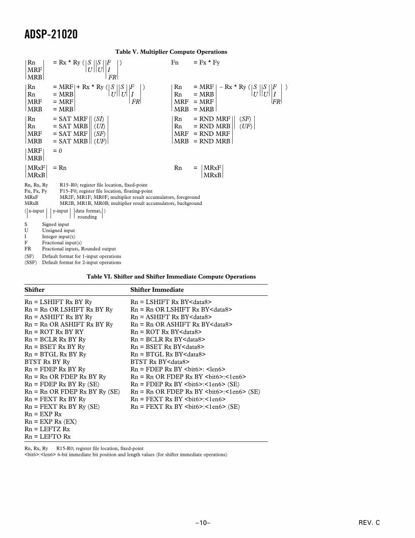
Table V. Multiplier Compute Operations
Rn = Rx * Ry ( S S F ) Fn = Fx * FyMRF = Rx * Ry ( U U IMRB = Rx * Ry ( U U FR
Rn = MRF + Rx * Ry ( S S F ) Rn = MRF – Rx * Ry ( S S F )Rn = MRB + Rx * Ry ( U U I Rn = MRB= Rx * Ry ( U U IMRF = MRF + Rx * Ry ( U U FR MRF = MRF= Rx * Ry ( U U I FRMRB = MRB MRB = MRB
Rn = SAT MRF (SI) Rn = RND MRF (SF)Rn = SAT MRB (UI) Rn = RND MRB (UF)MRF = SAT MRF (SF) MRF = RND MRFMRB = SAT MRB (UF) MRB = RND MRB
MRF = 0MRB
MRxF = Rn Rn = MRxFMRxB Rn = MRxB
Rn, Rx, Ry R15–R0; register file location, fixed-pointFn, Fx, Fy F15–F0; register file location, floating-pointMRxF MR2F, MR1F; MR0F; multiplier result accumulators, foregroundMRxB MR2B, MR1B, MR0B; multiplier result accumulators, background
( x-input y-input data format, )( x-input y-input rounding
S Signed inputU Unsigned inputI Integer input(s)F Fractional input(s)FR Fractional inputs, Rounded output
(SF) Default format for 1-input operations(SSF) Default format for 2-input operations
Table VI. Shifter and Shifter Immediate Compute Operations
Shifter Shifter Immediate
Rn = LSHIFT Rx BY Ry Rn = LSHIFT Rx BY<data8>Rn = Rn OR LSHIFT Rx BY Ry Rn = Rn OR LSHIFT Rx BY<data8>Rn = ASHIFT Rx BY Ry Rn = ASHIFT Rx BY<data8>Rn = Rn OR ASHIFT Rx BY Ry Rn = Rn OR ASHIFT Rx BY<data8>Rn = ROT Rx BY RY Rn = ROT Rx BY<data8>Rn = BCLR Rx BY Ry Rn = BCLR Rx BY<data8>Rn = BSET Rx BY Ry Rn = BSET Rx BY<data8>Rn = BTGL Rx BY Ry Rn = BTGL Rx BY<data8>BTST Rx BY Ry BTST Rx BY<data8>Rn = FDEP Rx BY Ry Rn = FDEP Rx BY <bit6>: <len6>Rn = Rn OR FDEP Rx BY Ry Rn = Rn OR FDEP Rx BY <bit6>:<1en6>Rn = FDEP Rx BY Ry (SE) Rn = FDEP Rx BY <bit6>:<1en6> (SE)Rn = Rn OR FDEP Rx BY Ry (SE) Rn = Rn OR FDEP Rx BY <bit6>:<1en6> (SE)Rn = FEXT Rx BY Ry Rn = FEXT Rx BY <bit6>:<1en6>Rn = FEXT Rx BY Ry (SE) Rn = FEXT Rx BY <bit6>:<1en6> (SE)Rn = EXP RxRn = EXP Rx (EX)Rn = LEFTZ RxRn = LEFTO Rx
Rn, Rx, Ry R15-R0; register file location, fixed-point<bit6>:<len6> 6-bit immediate bit position and length values (for shifter immediate operations)
ADSP-21020
REV. C –11–
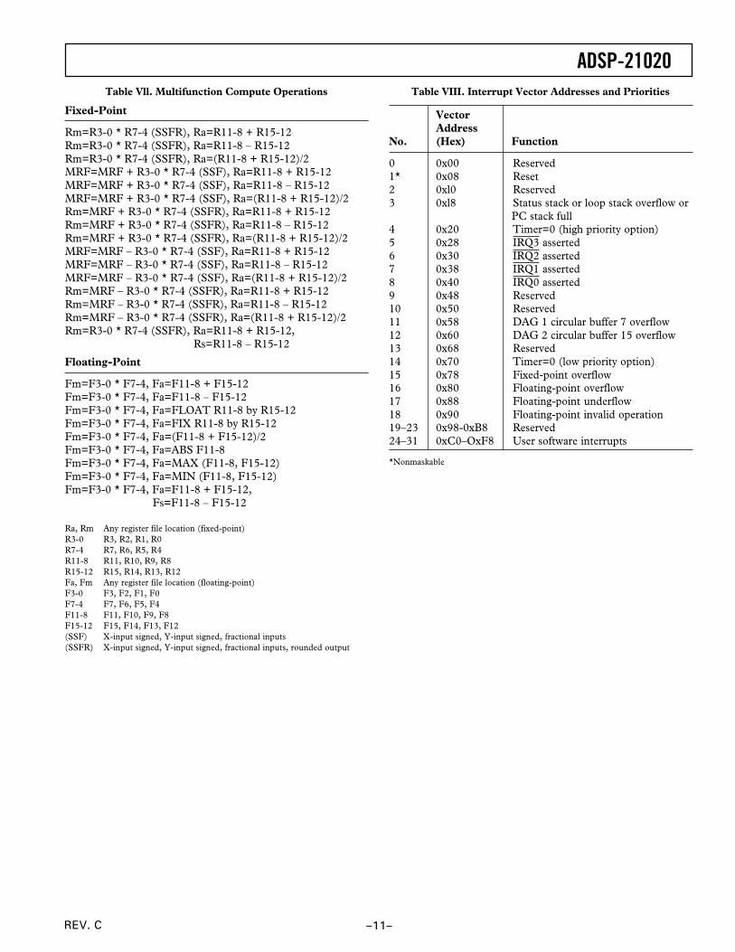
Table Vll. Multifunction Compute Operations
Fixed-Point
Rm=R3-0 * R7-4 (SSFR), Ra=R11-8 + R15-12Rm=R3-0 * R7-4 (SSFR), Ra=R11-8 – R15-12Rm=R3-0 * R7-4 (SSFR), Ra=(R11-8 + R15-12)/2MRF=MRF + R3-0 * R7-4 (SSF), Ra=R11-8 + R15-12MRF=MRF + R3-0 * R7-4 (SSF), Ra=R11-8 – R15-12MRF=MRF + R3-0 * R7-4 (SSF), Ra=(R11-8 + R15-12)/2Rm=MRF + R3-0 * R7-4 (SSFR), Ra=R11-8 + R15-12Rm=MRF + R3-0 * R7-4 (SSFR), Ra=R11-8 – R15-12Rm=MRF + R3-0 * R7-4 (SSFR), Ra=(R11-8 + R15-12)/2MRF=MRF – R3-0 * R7-4 (SSF), Ra=R11-8 + R15-12MRF=MRF – R3-0 * R7-4 (SSF), Ra=R11-8 – R15-12MRF=MRF – R3-0 * R7-4 (SSF), Ra=(R11-8 + R15-12)/2Rm=MRF – R3-0 * R7-4 (SSFR), Ra=R11-8 + R15-12Rm=MRF – R3-0 * R7-4 (SSFR), Ra=R11-8 – R15-12Rm=MRF – R3-0 * R7-4 (SSFR), Ra=(R11-8 + R15-12)/2Rm=R3-0 * R7-4 (SSFR), Ra=R11-8 + R15-12,
Rs=R11-8 – R15-12
Floating-Point
Fm=F3-0 * F7-4, Fa=F11-8 + F15-12Fm=F3-0 * F7-4, Fa=F11-8 – F15-12Fm=F3-0 * F7-4, Fa=FLOAT R11-8 by R15-12Fm=F3-0 * F7-4, Fa=FIX R11-8 by R15-12Fm=F3-0 * F7-4, Fa=(F11-8 + F15-12)/2Fm=F3-0 * F7-4, Fa=ABS F11-8Fm=F3-0 * F7-4, Fa=MAX (F11-8, F15-12)Fm=F3-0 * F7-4, Fa=MIN (F11-8, F15-12)Fm=F3-0 * F7-4, Fa=F11-8 + F15-12,
Fs=F11-8 – F15-12
Ra, Rm Any register file location (fixed-point)R3-0 R3, R2, R1, R0R7-4 R7, R6, R5, R4R11-8 R11, R10, R9, R8R15-12 R15, R14, R13, R12Fa, Fm Any register file location (floating-point)F3-0 F3, F2, F1, F0F7-4 F7, F6, F5, F4F11-8 F11, F10, F9, F8F15-12 F15, F14, F13, F12(SSF) X-input signed, Y-input signed, fractional inputs(SSFR) X-input signed, Y-input signed, fractional inputs, rounded output
Table VIII. Interrupt Vector Addresses and Priorities
VectorAddress
No. (Hex) Function
0 0x00 Reserved1* 0x08 Reset2 0xl0 Reserved3 0xl8 Status stack or loop stack overflow or
PC stack full4 0x20 Timer=0 (high priority option)5 0x28 IRQ3 asserted6 0x30 IRQ2 asserted7 0x38 IRQ1 asserted8 0x40 IRQ0 asserted9 0x48 Reserved10 0x50 Reserved11 0x58 DAG 1 circular buffer 7 overflow12 0x60 DAG 2 circular buffer 15 overflow13 0x68 Reserved14 0x70 Timer=0 (low priority option)15 0x78 Fixed-point overflow16 0x80 Floating-point overflow17 0x88 Floating-point underflow18 0x90 Floating-point invalid operation19–23 0x98-0xB8 Reserved24–31 0xC0–OxF8 User software interrupts
*Nonmaskable
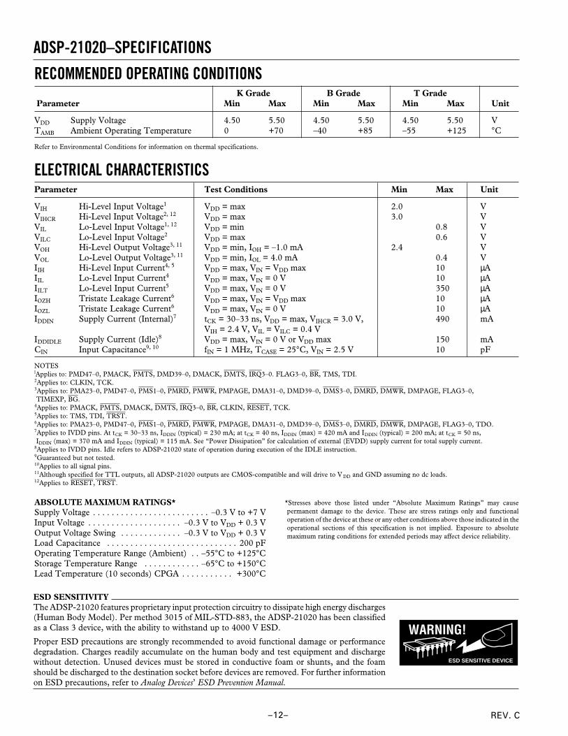
RECOMMENDED OPERATING CONDITIONS K Grade B Grade T Grade
Parameter Min Max Min Max Min Max Unit
VDD Supply Voltage 4.50 5.50 4.50 5.50 4.50 5.50 VTAMB Ambient Operating Temperature 0 +70 –40 +85 –55 +125 °C
Refer to Environmental Conditions for information on thermal specifications.
ELECTRICAL CHARACTERISTICSParameter Test Conditions Min Max Unit
VIH Hi-Level Input Voltage1 VDD = max 2.0 VVIHCR Hi-Level Input Voltage2, 12 VDD = max 3.0 VVIL Lo-Level Input Voltage1, 12 VDD = min 0.8 VVILC Lo-Level Input Voltage2 VDD = max 0.6 VVOH Hi-Level Output Voltage3, 11 VDD = min, IOH = –1.0 mA 2.4 VVOL Lo-Level Output Voltage3, 11 VDD = min, IOL = 4.0 mA 0.4 VIIH Hi-Level Input Current4, 5 VDD = max, VIN = VDD max 10 µAIIL Lo-Level Input Current4 VDD = max, VIN = 0 V 10 µAIILT Lo-Level Input Current5 VDD = max, VIN = 0 V 350 µAIOZH Tristate Leakage Current6 VDD = max, VIN = VDD max 10 µAIOZL Tristate Leakage Current6 VDD = max, VIN = 0 V 10 µAIDDIN Supply Current (Internal)7 tCK = 30–33 ns, VDD = max, VIHCR = 3.0 V, 490 mA
VIH = 2.4 V, VIL = VILC = 0.4 VIDDIDLE Supply Current (Idle)8 VDD = max, VIN = 0 V or VDD max 150 mACIN Input Capacitance9, 10 fIN = 1 MHz, TCASE = 25°C, VIN = 2.5 V 10 pF
NOTESlApplies to: PMD47–0, PMACK, PMTS, DMD39–0, DMACK, DMTS, IRQ3–0. FLAG3–0, BR, TMS, TDI.2Applies to: CLKIN, TCK.3Applies to: PMA23–0, PMD47–0, PMS1–0, PMRD, PMWR, PMPAGE, DMA31–0, DMD39–0, DMS3–0, DMRD, DMWR, DMPAGE, FLAG3–0,TIMEXP, BG.
4Applies to: PMACK, PMTS, DMACK, DMTS, IRQ3–0, BR, CLKIN, RESET, TCK.5Applies to: TMS, TDI, TRST.6Applies to: PMA23–0, PMD47–0, PMS1–0, PMRD, PMWR, PMPAGE, DMA31–0, DMD39–0, DMS3–0, DMRD, DMWR, DMPAGE, FLAG3–0, TDO.7Applies to IVDD pins. At tCK = 30–33 ns, IDDIN (typical) = 230 mA; at tCK = 40 ns, IDDIN (max) = 420 mA and IDDIN (typical) = 200 mA; at tCK = 50 ns,IDDIN (max) = 370 mA and IDDIN (typical) = 115 mA. See “Power Dissipation” for calculation of external (EVDD) supply current for total supply current.
8Applies to IVDD pins. Idle refers to ADSP-21020 state of operation during execution of the IDLE instruction.9Guaranteed but not tested.10Applies to all signal pins.11Although specified for TTL outputs, all ADSP-21020 outputs are CMOS-compatible and will drive to V DD and GND assuming no dc loads.12Applies to RESET, TRST.
ABSOLUTE MAXIMUM RATINGS*Supply Voltage . . . . . . . . . . . . . . . . . . . . . . . . . –0.3 V to +7 VInput Voltage . . . . . . . . . . . . . . . . . . . . –0.3 V to VDD + 0.3 VOutput Voltage Swing . . . . . . . . . . . . . –0.3 V to VDD + 0.3 VLoad Capacitance . . . . . . . . . . . . . . . . . . . . . . . . . . . . 200 pFOperating Temperature Range (Ambient) . . –55°C to +125°CStorage Temperature Range . . . . . . . . . . . . –65°C to +150°CLead Temperature (10 seconds) CPGA . . . . . . . . . . . +300°C
ESD SENSITIVITYThe ADSP-21020 features proprietary input protection circuitry to dissipate high energy discharges(Human Body Model). Per method 3015 of MIL-STD-883, the ADSP-21020 has been classifiedas a Class 3 device, with the ability to withstand up to 4000 V ESD.
Proper ESD precautions are strongly recommended to avoid functional damage or performancedegradation. Charges readily accumulate on the human body and test equipment and dischargewithout detection. Unused devices must be stored in conductive foam or shunts, and the foamshould be discharged to the destination socket before devices are removed. For further informationon ESD precautions, refer to Analog Devices’ ESD Prevention Manual.
*Stresses above those listed under “Absolute Maximum Ratings” may causepermanent damage to the device. These are stress ratings only and functionaloperation of the device at these or any other conditions above those indicated in theoperational sections of this specification is not implied. Exposure to absolutemaximum rating conditions for extended periods may affect device reliability.
REV. C–12–
ADSP-21020–SPECIFICATIONS
WARNING!
ESD SENSITIVE DEVICE
ADSP-21020
REV. C –13–
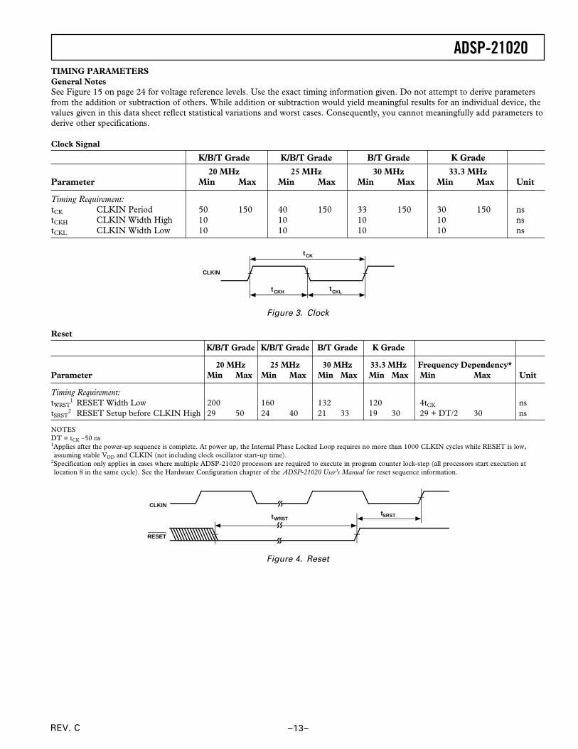
TIMING PARAMETERSGeneral NotesSee Figure 15 on page 24 for voltage reference levels. Use the exact timing information given. Do not attempt to derive parametersfrom the addition or subtraction of others. While addition or subtraction would yield meaningful results for an individual device, thevalues given in this data sheet reflect statistical variations and worst cases. Consequently, you cannot meaningfully add parameters toderive other specifications.
Clock Signal
K/B/T Grade K/B/T Grade B/T Grade K Grade
20 MHz 25 MHz 30 MHz 33.3 MHzParameter Min Max Min Max Min Max Min Max Unit
Timing Requirement:tCK CLKIN Period 50 150 40 150 33 150 30 150 nstCKH CLKIN Width High 10 10 10 10 nstCKL CLKIN Width Low 10 10 10 10 ns
CLKIN
tCKH tCKL
tCK
Figure 3. Clock
Reset
K/B/T Grade K/B/T Grade B/T Grade K Grade
20 MHz 25 MHz 30 MHz 33.3 MHz Frequency Dependency*Parameter Min Max Min Max Min Max Min Max Min Max Unit
Timing Requirement:tWRST
1 RESET Width Low 200 160 132 120 4tCK nstSRST
2 RESET Setup before CLKIN High 29 50 24 40 21 33 19 30 29 + DT/2 30 ns
NOTESDT = tCK –50 ns1Applies after the power-up sequence is complete. At power up, the Internal Phase Locked Loop requires no more than 1000 CLKIN cycles while RESET is low,assuming stable VDD and CLKIN (not including clock oscillator start-up time).
2Specification only applies in cases where multiple ADSP-21020 processors are required to execute in program counter lock-step (all processors start execution atlocation 8 in the same cycle). See the Hardware Configuration chapter of the ADSP-21020 User’s Manual for reset sequence information.
CLKIN
tWRSTtSRST
RESET
Figure 4. Reset
ADSP-21020
REV. C–14–
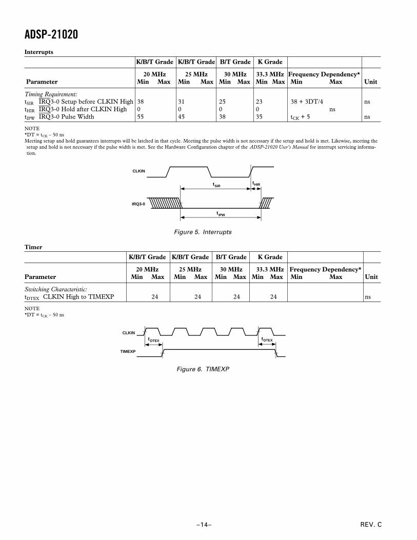
Interrupts
K/B/T Grade K/B/T Grade B/T Grade K Grade
20 MHz 25 MHz 30 MHz 33.3 MHz Frequency Dependency* Parameter Min Max Min Max Min Max Min Max Min Max Unit
Timing Requirement:tSIR IRQ3-0 Setup before CLKIN High 38 31 25 23 38 + 3DT/4 nstHIR IRQ3-0 Hold after CLKIN High 0 0 0 0 nstIPW IRQ3-0 Pulse Width 55 45 38 35 tCK + 5 ns
NOTE*DT = tCK – 50 nsMeeting setup and hold guarantees interrupts will be latched in that cycle. Meeting the pulse width is not necessary if the setup and hold is met. Likewise, meeting thesetup and hold is not necessary if the pulse width is met. See the Hardware Configuration chapter of the ADSP-21020 User’s Manual for interrupt servicing informa-tion.
CLKIN
tSIR
IRQ3-0
tHIR
tIPW
Figure 5. Interrupts
Timer
K/B/T Grade K/B/T Grade B/T Grade K Grade
20 MHz 25 MHz 30 MHz 33.3 MHz Frequency Dependency*Parameter Min Max Min Max Min Max Min Max Min Max Unit
Switching Characteristic:tDTEX CLKIN High to TIMEXP 24 24 24 24 ns
NOTE*DT = tCK – 50 ns
CLKIN
tDTEX
TIMEXP
tDTEX
Figure 6. TIMEXP
ADSP-21020
REV. C –15–
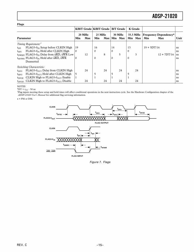
Flags
K/B/T Grade K/B/T Grade B/T Grade K Grade
20 MHz 25 MHz 30 MHz 33.3 MHz Frequency Dependency*Parameter Min Max Min Max Min Max Min Max Min Max Unit
Timing Requirement:1
tSFI FLAG3-0IN Setup before CLKIN High 19 16 14 13 19 + 5DT/16 nstHFI FLAG3-0IN Hold after CLKIN High 0 0 0 0 nstDWRFI FLAG3-0IN Delay from xRD, xWR Low 12 8 5 3 12 + 7DT/16 nstHFIWR FLAG3-0IN Hold after xRD, xWR 0 0 0 0 ns
Deasserted
Switching Characteristic:tDFO FLAG3-0OUT Delay from CLKIN High 24 24 24 24 nstHFO FLAG3-0OUT Hold after CLKIN High 5 5 5 5 nstDFOE CLKIN High to FLAG3-0OUT Enable 1 1 1 1 nstDFOD CLKIN High to FLAG3-0OUT Disable 24 24 24 24 ns
NOTES*DT = tCK – 50 ns1Flag inputs meeting these setup and hold times will affect conditional operations in the next instruction cycle. See the Hardware Configuration chapter of theADSP-21020 User’s Manual for additional flag servicing information.
x = PM or DM.
CLKIN
tDFOE
FLAG3-0OUT
tDFO tHFO
tDFO
tDFOD
FLAG OUTPUT
CLKIN
tHFI
FLAG3-0 IN
FLAG INPUT
tSFI
tDWRFItHFIWR
xRD, xWR
Figure 7. Flags
ADSP-21020
REV. C–16–
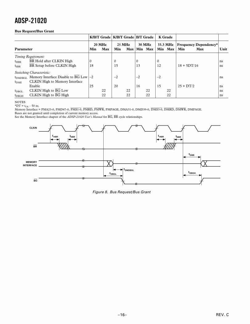
Bus Request/Bus Grant
K/B/T Grade K/B/T Grade B/T Grade K Grade
20 MHz 25 MHz 30 MHz 33.3 MHz Frequency Dependency*Parameter Min Max Min Max Min Max Min Max Min Max Unit
Timing Requirement:tHBR BR Hold after CLKIN High 0 0 0 0 nstSBR BR Setup before CLKIN High 18 15 13 12 18 + 5DT/16 ns
Switching Characteristic:tDMDBGL Memory Interface Disable to BG Low –2 –2 –2 –2 nstDME CLKIN High to Memory Interface
Enable 25 20 16 15 25 + DT/2 nstDBGL CLKIN High to BG Low 22 22 22 22 nstDBGH CLKIN High to BG High 22 22 22 22 ns
NOTES*DT = tCK – 50 ns.Memory Interface = PMA23-0, PMD47-0, PMS1-0, PMRD, PMWR, PMPAGE, DMA31-0, DMD39-0, DMS3-0, DMRD, DMWR, DMPAGE.Buses are not granted until completion of current memory access.See the Memory Interface chapter of the ADSP-21020 User’s Manual for BG, BR cycle relationships.
CLKIN
tHBR
MEMORYINTERFACE
tSBR
tDBGL
tDMDBGL
tHBR tSBR
tDME
tDBGH
BR
BG
Figure 8. Bus Request/Bus Grant
ADSP-21020
REV. C –17–
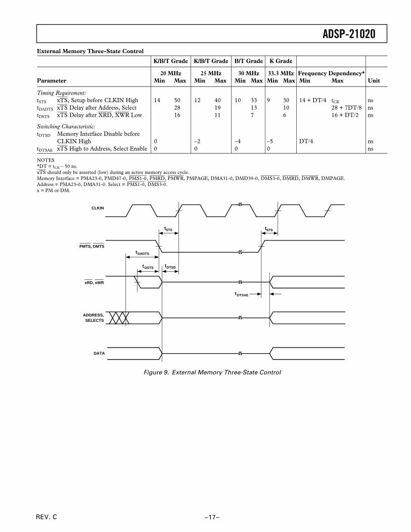
External Memory Three-State Control
K/B/T Grade K/B/T Grade B/T Grade K Grade
20 MHz 25 MHz 30 MHz 33.3 MHz Frequency Dependency*Parameter Min Max Min Max Min Max Min Max Min Max Unit
Timing Requirement:tSTS xTS, Setup before CLKIN High 14 50 12 40 10 33 9 30 14 + DT/4 tCK nstDADTS xTS Delay after Address, Select 28 19 13 10 28 + 7DT/8 nstDSTS xTS Delay after XRD, XWR Low 16 11 7 6 16 + DT/2 ns
Switching Characteristic:tDTSD Memory Interface Disable before
CLKIN High 0 –2 –4 –5 DT/4 nstDTSAE xTS High to Address, Select Enable 0 0 0 0 ns
NOTES*DT = tCK – 50 ns.xTS should only be asserted (low) during an active memory access cycle.Memory Interface = PMA23-0, PMD47-0, PMS1-0, PMRD, PMWR, PMPAGE, DMA31-0, DMD39-0, DMS3-0, DMRD, DMWR, DMPAGE.Address = PMA23-0, DMA31-0. Select = PMS1-0, DMS3-0.x = PM or DM.
CLKIN
ADDRESS,SELECTS
tSTS
DATA
tDTSD
tDADTS
tDTSAE
tDSTS
tSTS
xRD, xWR
PMTS, DMTS
Figure 9. External Memory Three-State Control
ADSP-21020
REV. C–18–
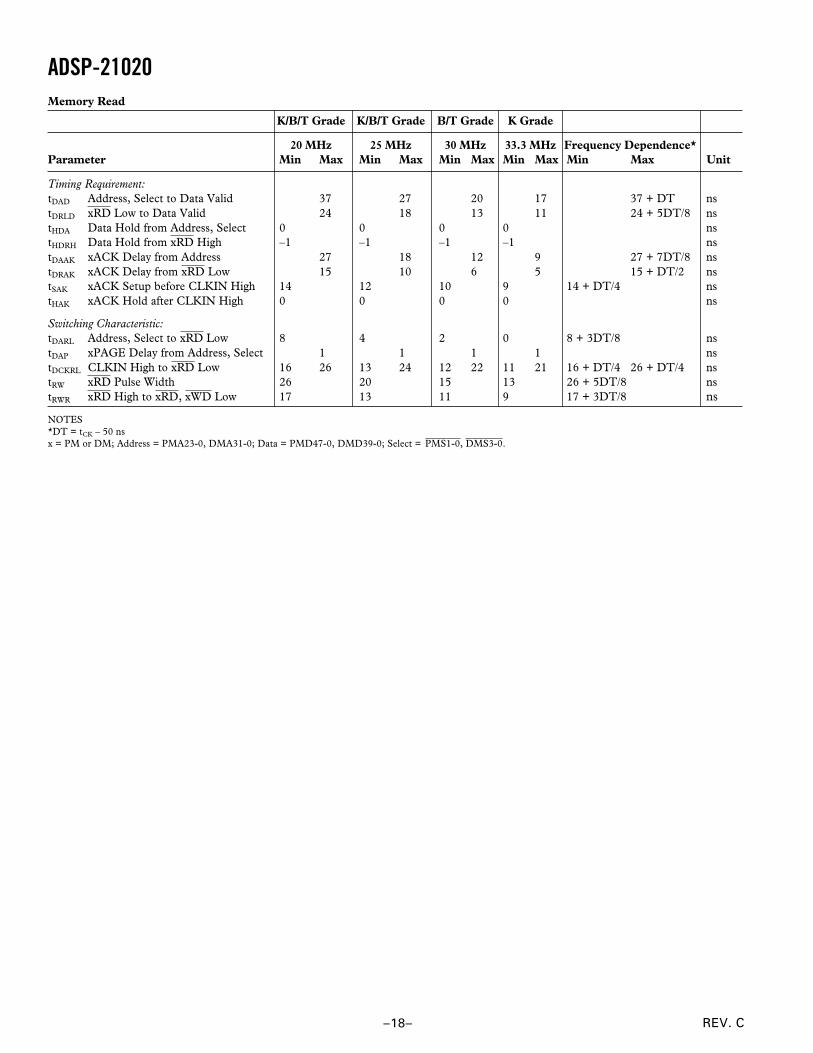
Memory Read
K/B/T Grade K/B/T Grade B/T Grade K Grade
20 MHz 25 MHz 30 MHz 33.3 MHz Frequency Dependence*Parameter Min Max Min Max Min Max Min Max Min Max Unit
Timing Requirement:tDAD Address, Select to Data Valid 37 27 20 17 37 + DT nstDRLD xRD Low to Data Valid 24 18 13 11 24 + 5DT/8 nstHDA Data Hold from Address, Select 0 0 0 0 nstHDRH Data Hold from xRD High –1 –1 –1 –1 nstDAAK xACK Delay from Address 27 18 12 9 27 + 7DT/8 nstDRAK xACK Delay from xRD Low 15 10 6 5 15 + DT/2 nstSAK xACK Setup before CLKIN High 14 12 10 9 14 + DT/4 nstHAK xACK Hold after CLKIN High 0 0 0 0 ns
Switching Characteristic:tDARL Address, Select to xRD Low 8 4 2 0 8 + 3DT/8 nstDAP xPAGE Delay from Address, Select 1 1 1 1 nstDCKRL CLKIN High to xRD Low 16 26 13 24 12 22 11 21 16 + DT/4 26 + DT/4 nstRW xRD Pulse Width 26 20 15 13 26 + 5DT/8 nstRWR xRD High to xRD, xWD Low 17 13 11 9 17 + 3DT/8 ns
NOTES*DT = tCK – 50 nsx = PM or DM; Address = PMA23-0, DMA31-0; Data = PMD47-0, DMD39-0; Select = PMS1-0, DMS3-0.
ADSP-21020
REV. C –19–
CLKIN
DATA
DMACK,PMACK
ADDRESS,SELECT
DMPAGE,PMPAGE
tDARL
tDAP
tDAAK
tDCKRL
tDRAKtSAK tHAK
tDAD
tDRLD
tRWR
tHDRH
tRW
tHDA
DMWR,PMWR
DMRD, PMRD
Figure 10. Memory Read
ADSP-21020
REV. C–20–
Memory Write
K/B/T Grade K/B/T Grade B/T Grade K Grade
20 MHz 25 MHz 30 MHz 33.3 MHz Frequency Dependency*Parameter Min Max Min Max Min Max Min Max Min Max Unit
Timing Requirement: 12tDAAK xACK Delay from Address, Select 27 18 6 9 27 + 7DT/8 nstDWAK xACK Delay from xWR Low 15 10 10 5 15 + DT/2 nstSAK xACK Setup before CLKIN High 14 12 0 9 14 + DT/4 nstHAK xACK Hold after CLKIN High 0 0 0 ns
Switching Characteristic:tDAWH Address, Select to xWR Deasserted 37 28 21 18 37+ 15DT/16 nstDAWL Address, Select to xWR Low 11 7 5 3 11 + 3DT/8 nstWW xWR Pulse Width 26 20 16 15 26 + 9DT/16 nstDDWH Data Setup before xWR High 23 18 14 13 23 + DT/2 nstDWHA Address, Select Hold after xWR
Deasserted 1 0 0 0 1 + DT/16 nstHDWH Data Hold after xWR Deasserted1 0 –1 –1 –1 DT/16 nstDAP xPAGE Delay from Address, Select 1 1 1 1 nstDCKWL CLKIN High to xWR Low 16 26 13 24 12 22 11 21 16 + DT/4 26 + DT/4 nstWWR xWR High to xWR or xRD Low 17 13 10 8 17 + 7DT/16 nstDDWR Data Disable before xWR or xRD
Low 13 9 7 5 13 + 3DT/8 nstWDE xWR Low to Data Enabled 0 –1 –1 –1 DT/16 ns
NOTES*DT = tC – 50 nsSee “System Hold Time Calculation” in “Test Conditions” section for calculating hold times given capacitive and DC loads.x = PM or DM; Address = PMA23-0, DMA31-0; Data = PMD47-0, DMD39-0; Select = PMS1-0, DMS3-0.
ADSP-21020
REV. C –21–
CLKIN
DATA
DMACK,PMACK
ADDRESS,SELECT
DMPAGE,PMPAGE
tDAWL
tDAP
tDAAK
tDCKWL
tDWAK
tSAK tHAK
tWDE
tDWHA
tWWR
tDDWR
tDDWH
tWW
tDAWH
tHDWH
DMWR,PMWR
DMRD,PMRD
Figure 11. Memory Write
ADSP-21020
REV. C–22–
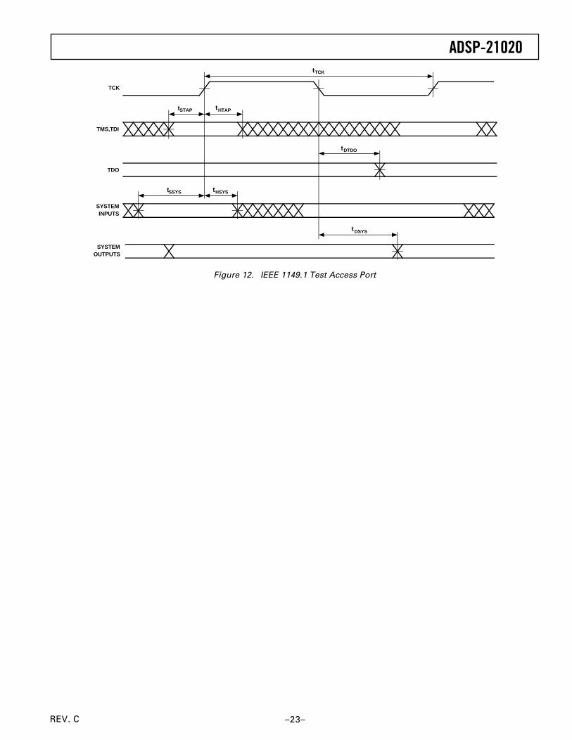
IEEE 1149.1 Test Access Port
K/B/T Grade K/B/T Grade B/T Grade K Grade
20 MHz 25 MHz 30 MHz 33.3 MHz Frequency Dependency*Parameter Min Max Min Max Min Max Min Max Min Max Unit
Timing Requirement:tTCK TCK Period 50 40 33 30 tCK nstSTAP TDI, TMS Setup before TCK High 5 5 5 5 nstHTAP TDI, TMS Hold after TCK High 6 6 6 6 nstSSYS System Inputs Setup before TCK High 7 7 7 7 nstHSYS System Inputs Hold after TCK High 9 9 9 9 nstTRSTW TRST Pulse Width 200 160 132 120 ns
Switching Characteristic:tDTDO TDO Delay from TCK Low 15 15 15 15 nstDSYS System Outputs Delay from TCK Low 26 26 26 26 ns
NOTES*DT = tC – 50 nsSystem Inputs = PMD47-0, PMACK, PMTS, DMD39-0, DMACK, DMTS, CLKIN, IRQ3 0, RESET, FLAG3-0, BR.System Outputs = PMA23-0, PMS1-0, PMRD, PMWR, PMD47-0, PMPAGE, DMA31-0, DMS1-0, DMRD, DMWR, DMD39-0, DMPAGE, FLAG3-0, BG,TIMEXP.See the IEEE 1149.1 Test Access Port chapter of the ADSP-21020 User’s Manual for further detail.
ADSP-21020
REV. C –23–
TCK
TMS,TDI
TDO
SYSTEMINPUTS
SYSTEMOUTPUTS
tSTAP tHTAP
tDTDO
tSSYS tHSYS
tDSYS
tTCK
Figure 12. IEEE 1149.1 Test Access Port
ADSP-21020
REV. C–24–
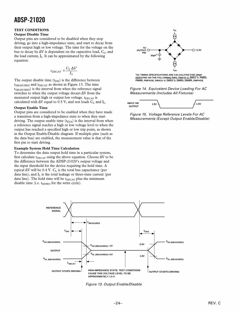
TEST CONDITIONSOutput Disable TimeOutput pins are considered to be disabled when they stopdriving, go into a high-impedance state, and start to decay fromtheir output high or low voltage. The time for the voltage on thebus to decay by ∆V is dependent on the capacitive load, CL, andthe load current, IL. It can be approximated by the followingequation:
tDECAY =
CL ∆VIL
The output disable time (tDIS) is the difference betweentMEASURED and tDECAY as shown in Figure 13. The timetMEASURED) is the interval from when the reference signalswitches to when the output voltage decays ∆V from themeasured output high or output low voltage. tDECAY iscalculated with ∆V equal to 0.5 V, and test loads CL and IL.
Output Enable TimeOutput pins are considered to be enabled when they have madea transition from a high-impedance state to when they startdriving. The output enable time (tENA) is the interval from whena reference signal reaches a high or low voltage level to when theoutput has reached a specified high or low trip point, as shownin the Output Enable/Disable diagram. If multiple pins (such asthe data bus) are enabled, the measurement value is that of thefirst pin to start driving.
Example System Hold Time CalculationTo determine the data output hold time in a particular system,first calculate tDECAY using the above equation. Choose ∆V to bethe difference between the ADSP-21020’s output voltage andthe input threshold for the device requiring the hold time. Atypical ∆V will be 0.4 V. CL is the total bus capacitance (perdata line), and IL is the total leakage or three-state current (perdata line). The hold time will be tDECAY plus the minimumdisable time (i.e. tHDWD for the write cycle).
TOOUTPUT
PIN50pF*
+1.5V
*AC TIMING SPECIFICATIONS ARE CALCULATED FOR 100pFDERATING ON THE FOLLOWING PINS: PMA23–0, PMS1–0, PMRD,PMWR, PMPAGE, DMA31–0, DMS3–0, DMRD, DMWR, DMPAGE
IOH
IOL
Figure 14. Equivalent Device Loading For AC
Measurements (Includes All Fixtures)
INPUT OROUTPUT
1.5V1.5V
Figure 15. Voltage Reference Levels For AC
Measurements (Except Output Enable/Disable)
tENA
2.0V
1.0V
–∆V
+∆V
tDIS
REFERENCESIGNAL
OUTPUT
tDECAY
VOH (MEASURED)
VOL (MEASURED)
tMEASURED
OUTPUT STOPS DRIVING OUTPUT STARTS DRIVINGHIGH-IMPEDANCE STATE. TEST CONDITIONSCAUSE THIS VOLTAGE LEVEL TO BEAPPROXIMATELY 1.5 V.
VOH (MEASURED)
VOL (MEASURED)
VOH (MEASURED)
VOL (MEASURED)
Figure 13. Output Enable/Disable
ADSP-21020
REV. C –25–
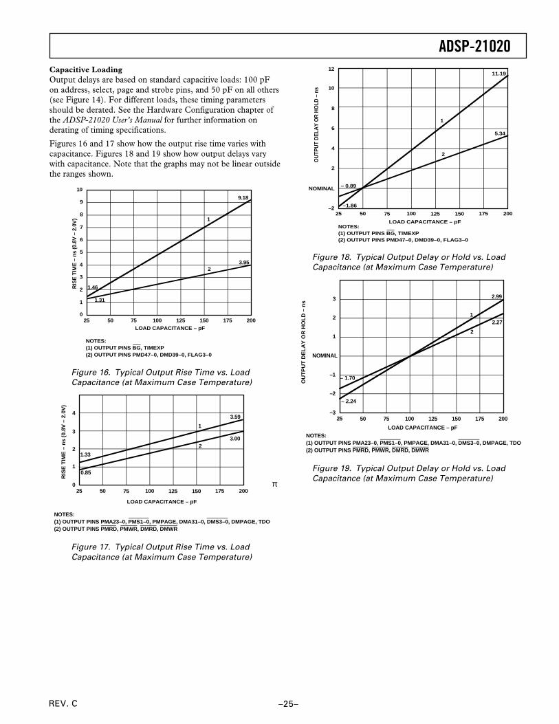
Capacitive LoadingOutput delays are based on standard capacitive loads: 100 pFon address, select, page and strobe pins, and 50 pF on all others(see Figure 14). For different loads, these timing parametersshould be derated. See the Hardware Configuration chapter ofthe ADSP-21020 User’s Manual for further information onderating of timing specifications.
Figures 16 and 17 show how the output rise time varies withcapacitance. Figures 18 and 19 show how output delays varywith capacitance. Note that the graphs may not be linear outsidethe ranges shown.
10
0200
3
1
50
2
25
6
4
5
7
8
9
17515012510075LOAD CAPACITANCE – pF
RIS
E T
IME
– n
s (0
.8V
– 2
.0V
) 1
2
9.18
1.46
1.31
NOTES:(1) OUTPUT PINS BG, TIMEXP(2) OUTPUT PINS PMD47–0, DMD39–0, FLAG3–0
3.95
Figure 16. Typical Output Rise Time vs. Load
Capacitance (at Maximum Case Temperature)
0200
3
1
50
2
25
4
17512510075 150
LOAD CAPACITANCE – pF
RIS
E T
IME
– n
s (0
.8V
– 2
.0V
)
1
2
3.59
3.00
1.33
0.85
NOTES:(1) OUTPUT PINS PMA23–0, PMS1–0, PMPAGE, DMA31–0, DMS3–0, DMPAGE, TDO(2) OUTPUT PINS PMRD, PMWR, DMRD, DMWR
π
Figure 17. Typical Output Rise Time vs. Load
Capacitance (at Maximum Case Temperature)
10
–2200
4
NOMINAL
50
2
25
8
6
17512510075 150
1
2
11.19
5.34
–1.86
– 0.89
LOAD CAPACITANCE – pF
OU
TPU
T D
ELA
Y O
R H
OLD
– n
s
NOTES:(1) OUTPUT PINS BG, TIMEXP(2) OUTPUT PINS PMD47–0, DMD39–0, FLAG3–0
12
Figure 18. Typical Output Delay or Hold vs. Load
Capacitance (at Maximum Case Temperature)
–3200
NOMINAL
–2
50
–1
25
3
1
2
17515012510075
1
2
2.99
2.27
– 1.70
– 2.24
LOAD CAPACITANCE – pF
OU
TP
UT
DE
LA
Y O
R H
OL
D –
ns
NOTES:(1) OUTPUT PINS PMA23–0, PMS1–0, PMPAGE, DMA31–0, DMS3–0, DMPAGE, TDO(2) OUTPUT PINS PMRD, PMWR, DMRD, DMWR
Figure 19. Typical Output Delay or Hold vs. Load
Capacitance (at Maximum Case Temperature)
ADSP-21020
REV. C–26–
ENVIRONMENTAL CONDITIONSThe ADSP-21020 is available in a Ceramic Pin Grid Array(CPGA). The package uses a cavity-down configuration whichgives it favorable thermal characteristics. The top surface of thepackage contains a raised copper slug from which much of thedie heat is dissipated. The slug provides a surface for mountinga heat sink (if required).
The commercial grade (K grade) ADSP-21020 is specified foroperation at TAMB of 0°C to +70°C. Maximum TCASE (casetemperature) can be calculated from the following equation:
TCASE = T AMB + PD × θCA( )where PD is power dissipation and θCA is the case-to-ambientthermal resistance. The value of PD depends on yourapplication; the method for calculating PD is shown under“Power Dissipation” below. θCA varies with airflow and with thepresence or absence of a heat sink. Table IX shows a range ofθCA values.
Table IX. Maximum θCA for Various Airflow Values
Airflow (Linear ft./min.) 0 100 200 300
CPGA with No Heat Sink 12.8°C/W 9.2°C/W 6.6°C/W 5.5°C/W
NOTESθJC is approximately 1°C/W.Maximum recommended TJ is 130°C.As per method 1012 MIL-STD-883. Ambient temperature: 25°C. Power:3.5 W.
Power DissipationTotal power dissipation has two components: one due tointernal circuitry and one due to the switching of externaloutput drivers. Internal power dissipation is dependent on theinstruction execution sequence and the data values involved.Internal power dissipation is calculated in the following way:
PINT = IDDIN 3 VDD
The external component of total power dissipation is caused bythe switching of output pins. Its magnitude depends on:
1) the number of output pins that switch during each cycle (O),2) the maximum frequency at which they can switch (f),3) their load capacitance (C), and4) their voltage swing (VDD).
It is calculated by:
PEXT = O 3 C 3 VDD2 3 f
The load capacitance should include the processor’s packagecapacitance (CIN). The switching frequency includes driving theload high and then back low. Address and data pins can drivehigh and low at a maximum rate of 1/(2tCK). The write strobescan switch every cycle at a frequency of 1/tCK. Select pins switchat 1/(2tCK), but 2 DM and 2 PM selects can switch on eachcycle. If only one bank is accessed, no select line will switch.
Example:
Estimate PEXT with the following assumptions:
• A system with one RAM bank each of PM (48 bits) and DM(32 bits).
• 32K 3 8 RAM chips are used, each with a load of 10 pF.
• Single-precision mode is enabled so that only 32 data pins canswitch at once.
• PM and DM writes occur every other cycle, with 50% of thepins switching.
• The instruction cycle rate is 20 MHz (tCK = 50 ns) andVDD = 5.0 V.
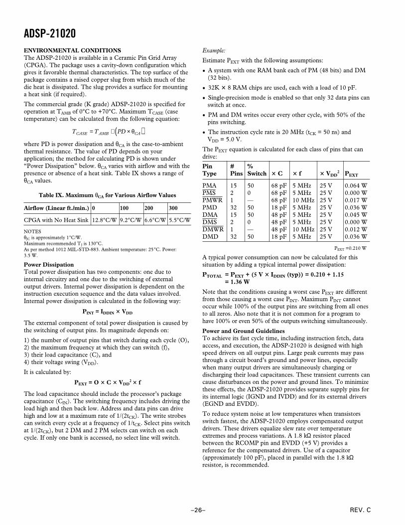
The PEXT equation is calculated for each class of pins that candrive:
Pin # %Type Pins Switch 3 C 3 f 3 VDD
2 PEXT
PMA 15 50 68 pF 5 MHz 25 V 0.064 WPMS 2 0 68 pF 5 MHz 25 V 0.000 WPMWR 1 — 68 pF 10 MHz 25 V 0.017 WPMD 32 50 18 pF 5 MHz 25 V 0.036 WDMA 15 50 48 pF 5 MHz 25 V 0.045 WDMS 2 0 48 pF 5 MHz 25 V 0.000 WDMWR 1 — 48 pF 10 MHz 25 V 0.012 WDMD 32 50 18 pF 5 MHz 25 V 0.036 W
PEXT =0.210 W
A typical power consumption can now be calculated for thissituation by adding a typical internal power dissipation:
PTOTAL = PEXT + (5 V 3 IDDIN (typ)) = 0.210 + 1.15= 1.36 W
Note that the conditions causing a worst case PEXT are differentfrom those causing a worst case PINT. Maximum PINT cannotoccur while 100% of the output pins are switching from all onesto all zeros. Also note that it is not common for a program tohave 100% or even 50% of the outputs switching simultaneously.
Power and Ground GuidelinesTo achieve its fast cycle time, including instruction fetch, dataaccess, and execution, the ADSP-21020 is designed with highspeed drivers on all output pins. Large peak currents may passthrough a circuit board’s ground and power lines, especiallywhen many output drivers are simultaneously charging ordischarging their load capacitances. These transient currents cancause disturbances on the power and ground lines. To minimizethese effects, the ADSP-21020 provides separate supply pins forits internal logic (IGND and IVDD) and for its external drivers(EGND and EVDD).
To reduce system noise at low temperatures when transistorsswitch fastest, the ADSP-21020 employs compensated outputdrivers. These drivers equalize slew rate over temperatureextremes and process variations. A 1.8 kΩ resistor placedbetween the RCOMP pin and EVDD (+5 V) provides areference for the compensated drivers. Use of a capacitor(approximately 100 pF), placed in parallel with the 1.8 kΩresistor, is recommended.
ADSP-21020
REV. C –27–
All GND pins should have a low impedance path to ground. Aground plane is required in ADSP-21020 systems to reduce thisimpedance, minimizing noise.
The EVDD and IVDD pins should be bypassed to the groundplane using approximately 14 high-frequency capacitors (0.1 µFceramic). Keep each capacitor’s lead and trace length to thepins as short as possible. This low inductive path provides theADSP-21020 with the peak currents required when its outputdrivers switch. The capacitors’ ground leads should also beshort and connect directly to the ground plane. This provides alow impedance return path for the load capacitance of theADSP-21020’s output drivers.
If a VDD plane is not used, the following recommendationsapply. Traces from the +5 V supply to the 10 EVDD pinsshould be designed to satisfy the minimum VDD specificationwhile carrying average dc currents of [IDDEX/10 3 (number ofEVDD pins per trace)]. IDDEX is the calculated external supplycurrent. A similar calculation should be made for the fourIVDD pins using the IDDIN specification. The traces connecting+5 V to the IVDD pins should be separate from those con-necting to the EVDD pins.
A low frequency bypass capacitor (20 µF tantalum) located nearthe junction of the IVDD and EVDD traces is also recommended.
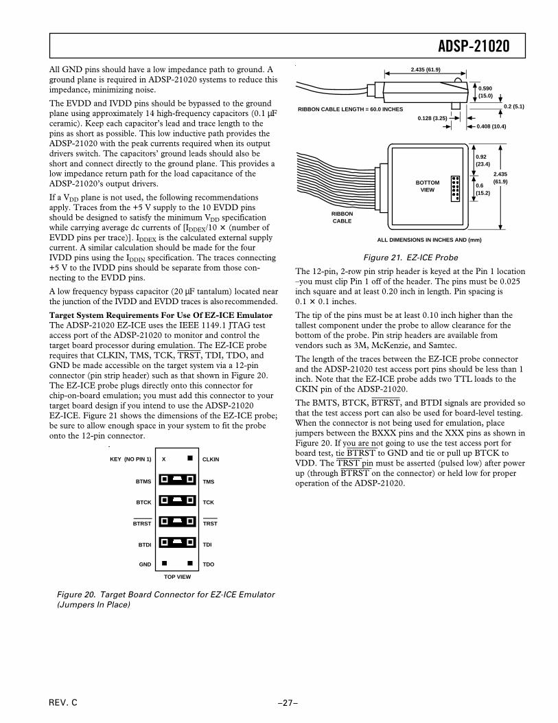
Target System Requirements For Use Of EZ-ICE EmulatorThe ADSP-21020 EZ-ICE uses the IEEE 1149.1 JTAG testaccess port of the ADSP-21020 to monitor and control thetarget board processor during emulation. The EZ-ICE proberequires that CLKIN, TMS, TCK, TRST, TDI, TDO, andGND be made accessible on the target system via a 12-pinconnector (pin strip header) such as that shown in Figure 20.The EZ-ICE probe plugs directly onto this connector forchip-on-board emulation; you must add this connector to yourtarget board design if you intend to use the ADSP-21020EZ-ICE. Figure 21 shows the dimensions of the EZ-ICE probe;be sure to allow enough space in your system to fit the probeonto the 12-pin connector.
CLKIN
TCK
TDI
TDO
TMS
TRST
BTCK
BTDI
GND
BTMS
BTRST
KEY (NO PIN 1)
TOP VIEW
X
Figure 20. Target Board Connector for EZ-ICE Emulator
(Jumpers In Place)
BOTTOMVIEW
2.435 (61.9)
0.6 (15.2)
0.92 (23.4)
RIBBONCABLE
ALL DIMENSIONS IN INCHES AND (mm)
0.590 (15.0)
2.435 (61.9)
0.2 (5.1)
0.128 (3.25)0.408 (10.4)
RIBBON CABLE LENGTH = 60.0 INCHES
Figure 21. EZ-ICE Probe
The 12-pin, 2-row pin strip header is keyed at the Pin 1 location–you must clip Pin 1 off of the header. The pins must be 0.025inch square and at least 0.20 inch in length. Pin spacing is0.1 3 0.1 inches.
The tip of the pins must be at least 0.10 inch higher than thetallest component under the probe to allow clearance for thebottom of the probe. Pin strip headers are available fromvendors such as 3M, McKenzie, and Samtec.
The length of the traces between the EZ-ICE probe connectorand the ADSP-21020 test access port pins should be less than 1inch. Note that the EZ-ICE probe adds two TTL loads to theCKIN pin of the ADSP-21020.
The BMTS, BTCK, BTRST, and BTDI signals are provided sothat the test access port can also be used for board-level testing.When the connector is not being used for emulation, placejumpers between the BXXX pins and the XXX pins as shown inFigure 20. If you are not going to use the test access port forboard test, tie BTRST to GND and tie or pull up BTCK toVDD. The TRST pin must be asserted (pulsed low) after powerup (through BTRST on the connector) or held low for properoperation of the ADSP-21020.
ADSP-21020
REV. C–28–
TCK
PMA21
PMPAGE
TRST
RCOMP
DMACK
TDO
DMTS
PMWR
PMD47
PMD46
PMD44
PMD42
PMD41
PMD38
DMD22
EVDD
DMD24
DMD25DMD26
DMD23
DMD27
DMD28
DMD33
DMD29
DMD35
DMD36
DMD39
DMD34
NC
DMS0
DMPAGE
DMS2
DMA31
DMA27
DMA26
DMA29
DMA24
DMA19
DMA14
DMA17
PMA0
NC
FLAG2
DMA1
DMA3
DMA7
DMA11
PMA20
PMA19
PMA14
PMA10
PMA9
PMA5
PMA4
BG
IRQ0
PMACK
NC
NC
RESET
DMD32
DMD30
DMD31
EGND
NC
PMD36
PMD33
EGND
DMA30
DMA28
DMA23
EVDD
DMA13
DMA16
EGND
EVDD
EGND
FLAG3
DMA2
DMA6
DMA9
PMA17
PMA11
PMA1
PMA8
BR
EGND
EGND
EVDD
EVDD
DMD7
DMD12
PMD31
PMD27
PMD9
PMD4
PMD1
DMD4
PMD21
PMD18
PMD12
EGND
EGND
EGND
EGND
EVDD
EVDD
PMS0
TDI
DMWR
EVDD
DMS3
DMS1
EGND
IGND
PMD45
PMD43
EGND
IGND
CLKIN
DMRD
EGND
IGND
DMD37
DMD38
EVDD
IVDD
DMA25
DMA15
DMA10
DMA5
FLAG1
PMA2
PMA7
PMA12
PMA16
PMA22
PMS1
DMA20
IRQ3
EGND
EGND
IGND
IGND
IVDD
NC
PMRD
EVDD
IVDD
DMA21
DMA22
TIMEXP
TMS
PMA23
DMA18
DMA12
DMA8
DMA4
DMA0
FLAG0
PMA3
PMA6
PMA15
PMA18
IRQ1
IRQ2
PMA13
DMD8
DMD14
PMD35
PMD30
PMD11
PMD8
PMD5
PMD3
NC
PMD0
DMD2
DMD5
PMD26
PMD23
PMD19
PMD16
PMD13
DMD16
DMD18
PMD39
PMD32
PMD10
PMD7
PMD2
PMD28
PMD25
PMD22
PMD17
PMD14
DMD0
DMD3
DMD6
DMD10
DMD11
DMD15
EGND
DMD21
PMD40
PMD37
PMD34
PMD29
PMD24
PMD20
PMD15
PMD6
DMD1
DMD9
DMD13
DMD17
DMD20
IGND
IGND
IVDD
DMD19
N
M
L
K
J
H
G
F
E
D
C
B
A
U
T
S
R
P
13 12 11 10 9 8 7 6 5 4 3 2 118 17 16 15 14
N
M
L
K
J
H
G
F
E
D
C
B
U
T
S
R
P
A
13 12 11 10 9 8 7 6 5 4 3 2 118 17 16 15 14
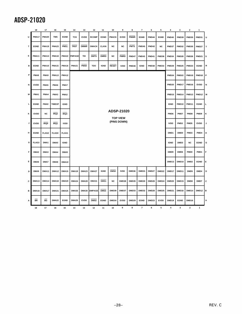
TOP VIEW(PINS DOWN)
PMTS
ADSP-21020
ADSP-21020
REV. C –29–
DMD7 DMD8 DMA14 DMA13
DMD12 DMD14 DMD18 DMD21
DMD22
DMD26 DMD32 DMD33 DMD37 DMD39 DMA21 DMA17 DMA16
EVDD DMD23 DMD29 DMD34 DMA22 BG BR
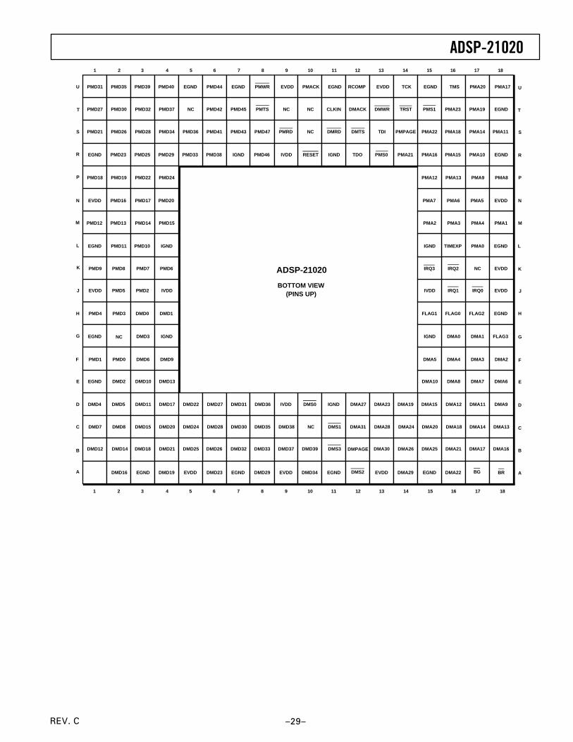
BOTTOM VIEW(PINS UP)
PMD31 PMD35 PMD39 PMD40 PMD44 PMWR PMACK RCOMP
PMD27 PMD30 PMD32 PMD37 NC PMD42 PMTS NC NC CLKIN DMACK DMWR
PMD11 PMA0 EGND
PMD9 PMD8 NC EVDD
PMD5 IRQ0
PMD4 PMD3 FLAG2 EGND
NC DMA1 FLAG3
PMD1 PMD0 DMA3 DMA2
DMD2 DMA7 DMA6
DMD4 DMD5 DMA11 DMA9
13121110987654321
N
M
L
K
J
H
G
F
E
D
C
B
13121110987654321
N
M
L
K
J
H
G
F
E
D
C
B
A
PMD47 PMRD NC
TIMEXP
IRQ2
IRQ1
PMD10
PMD7
PMD2
DMD35 DMD38 NC
TCK TMS PMA20 PMA17
TRST PMS1 PMA23 PMA19
DMS3 DMPAGE DMA30 DMA26 DMA25
DMS2 DMA29
PMD21 PMD26
PMD23
PMD18 PMD19
PMD16
PMD12 PMD13
PMA14 PMA11
PMA10
PMA9
PMA5
PMA4 PMA1
1817161514
U
T
S
R
P
1817161514
U
T
S
R
P
DMA18
DMA15 DMA12
DMA10 DMA8
DMA5 DMA4
DMA0
FLAG0FLAG1
PMA2 PMA3
PMA6PMA7
PMA8PMA12
PMA15PMA16
PMA18
PMA21
PMA22
PMS0
PMPAGE
TDO
TDIDMTSDMRD
PMD46
PMD45
PMD43PMD41
PMD38
PMD36PMD34
PMD33PMD29
PMD28
PMD25
PMD24PMD22
PMD20PMD17
PMD15PMD14
PMD6
DMD0 DMD1
DMD3
DMD6 DMD9
DMD10
DMD11
DMD13
DMD15
DMD17
DMD20 DMD24
DMD25
DMD27
DMD28 DMD30
DMD31 DMD36
DMS1
DMS0
DMA31 DMA28
DMA27
DMA24
DMA23
DMA20
DMA19
IRQ3
RESET
EGND EGND EGND
EGND
EGND
EGND
EGNDEGND
EGND
EGND EGND EGND EGND
EVDD EVDD
EVDD EVDD
EVDDEVDD
EVDD EVDD
IGND
IGND IGND
IGNDIGND
IGND IGND
IVDD
IVDD IVDD
IVDD
PMA13
DMD16 EGND DMD19A
ADSP-21020
ADSP-21020
REV. C–30–
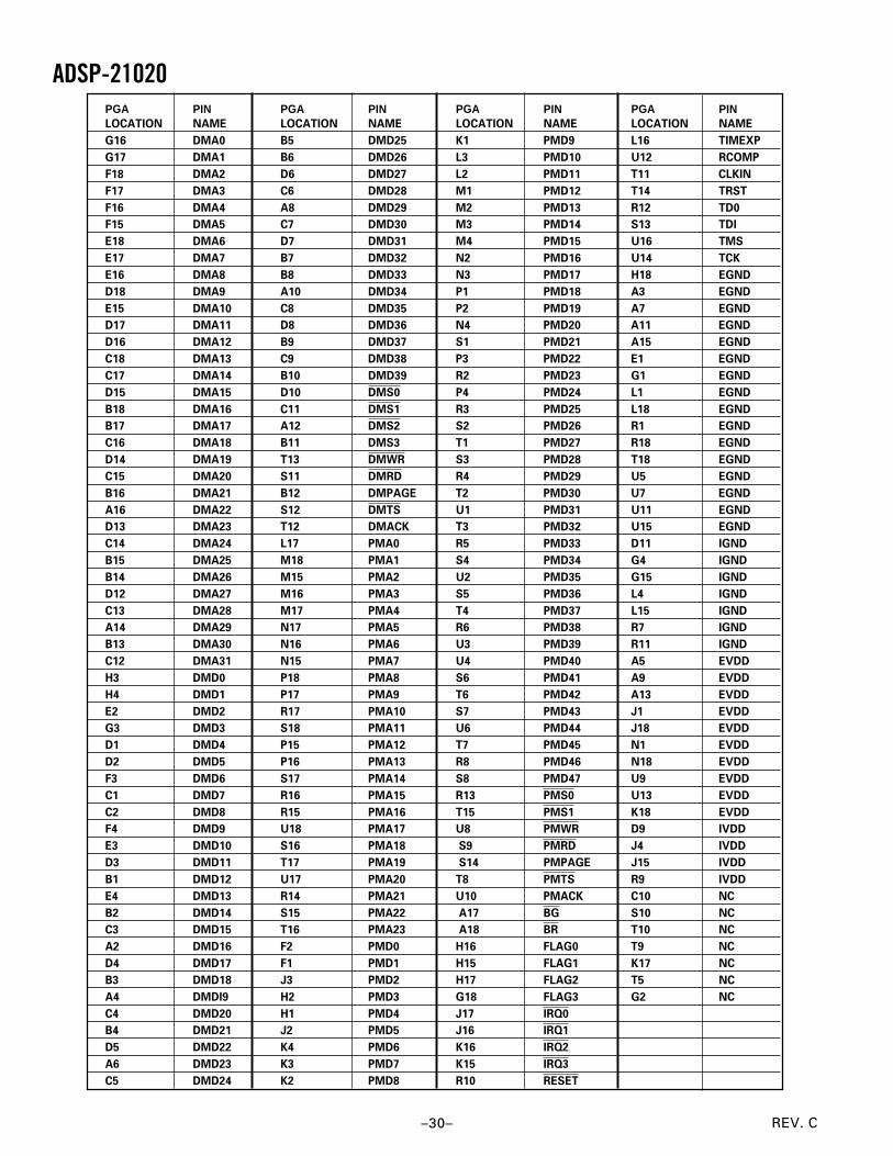
PGA PIN PGA PIN PGA PIN PGA PINLOCATION NAME LOCATION NAME LOCATION NAME LOCATION NAME
G16 DMA0 B5 DMD25 K1 PMD9 L16 TIMEXP
G17 DMA1 B6 DMD26 L3 PMD10 U12 RCOMP
F18 DMA2 D6 DMD27 L2 PMD11 T11 CLKIN
F17 DMA3 C6 DMD28 M1 PMD12 T14 TRST
F16 DMA4 A8 DMD29 M2 PMD13 R12 TD0
F15 DMA5 C7 DMD30 M3 PMD14 S13 TDI
E18 DMA6 D7 DMD31 M4 PMD15 U16 TMS
E17 DMA7 B7 DMD32 N2 PMD16 U14 TCK
E16 DMA8 B8 DMD33 N3 PMD17 H18 EGND
D18 DMA9 A10 DMD34 P1 PMD18 A3 EGND
E15 DMA10 C8 DMD35 P2 PMD19 A7 EGND
D17 DMA11 D8 DMD36 N4 PMD20 A11 EGND
D16 DMA12 B9 DMD37 S1 PMD21 A15 EGND
C18 DMA13 C9 DMD38 P3 PMD22 E1 EGND
C17 DMA14 B10 DMD39 R2 PMD23 G1 EGND
D15 DMA15 D10 DMS0 P4 PMD24 L1 EGND
B18 DMA16 C11 DMS1 R3 PMD25 L18 EGND
B17 DMA17 A12 DMS2 S2 PMD26 R1 EGND
C16 DMA18 B11 DMS3 T1 PMD27 R18 EGND
D14 DMA19 T13 DMWR S3 PMD28 T18 EGND
C15 DMA20 S11 DMRD R4 PMD29 U5 EGND
B16 DMA21 B12 DMPAGE T2 PMD30 U7 EGND
A16 DMA22 S12 DMTS U1 PMD31 U11 EGND
D13 DMA23 T12 DMACK T3 PMD32 U15 EGND
C14 DMA24 L17 PMA0 R5 PMD33 D11 IGND
B15 DMA25 M18 PMA1 S4 PMD34 G4 IGND
B14 DMA26 M15 PMA2 U2 PMD35 G15 IGND
D12 DMA27 M16 PMA3 S5 PMD36 L4 IGND
C13 DMA28 M17 PMA4 T4 PMD37 L15 IGND
A14 DMA29 N17 PMA5 R6 PMD38 R7 IGND
B13 DMA30 N16 PMA6 U3 PMD39 R11 IGND
C12 DMA31 N15 PMA7 U4 PMD40 A5 EVDD
H3 DMD0 P18 PMA8 S6 PMD41 A9 EVDD
H4 DMD1 P17 PMA9 T6 PMD42 A13 EVDD
E2 DMD2 R17 PMA10 S7 PMD43 J1 EVDD
G3 DMD3 S18 PMA11 U6 PMD44 J18 EVDD
D1 DMD4 P15 PMA12 T7 PMD45 N1 EVDD
D2 DMD5 P16 PMA13 R8 PMD46 N18 EVDD
F3 DMD6 S17 PMA14 S8 PMD47 U9 EVDD
C1 DMD7 R16 PMA15 R13 PMS0 U13 EVDD
C2 DMD8 R15 PMA16 T15 PMS1 K18 EVDD
F4 DMD9 U18 PMA17 U8 PMWR D9 IVDD
E3 DMD10 S16 PMA18 S9 PMRD J4 IVDD
D3 DMD11 T17 PMA19 S14 PMPAGE J15 IVDD
B1 DMD12 U17 PMA20 T8 PMTS R9 IVDD
E4 DMD13 R14 PMA21 U10 PMACK C10 NC
B2 DMD14 S15 PMA22 A17 BG S10 NC
C3 DMD15 T16 PMA23 A18 BR T10 NC
A2 DMD16 F2 PMD0 H16 FLAG0 T9 NC
D4 DMD17 F1 PMD1 H15 FLAG1 K17 NC
B3 DMD18 J3 PMD2 H17 FLAG2 T5 NC
A4 DMDl9 H2 PMD3 G18 FLAG3 G2 NC
C4 DMD20 H1 PMD4 J17 IRQ0B4 DMD21 J2 PMD5 J16 IRQ1D5 DMD22 K4 PMD6 K16 IRQ2A6 DMD23 K3 PMD7 K15 IRQ3C5 DMD24 K2 PMD8 R10 RESET
ADSP-21020
REV. C –31–
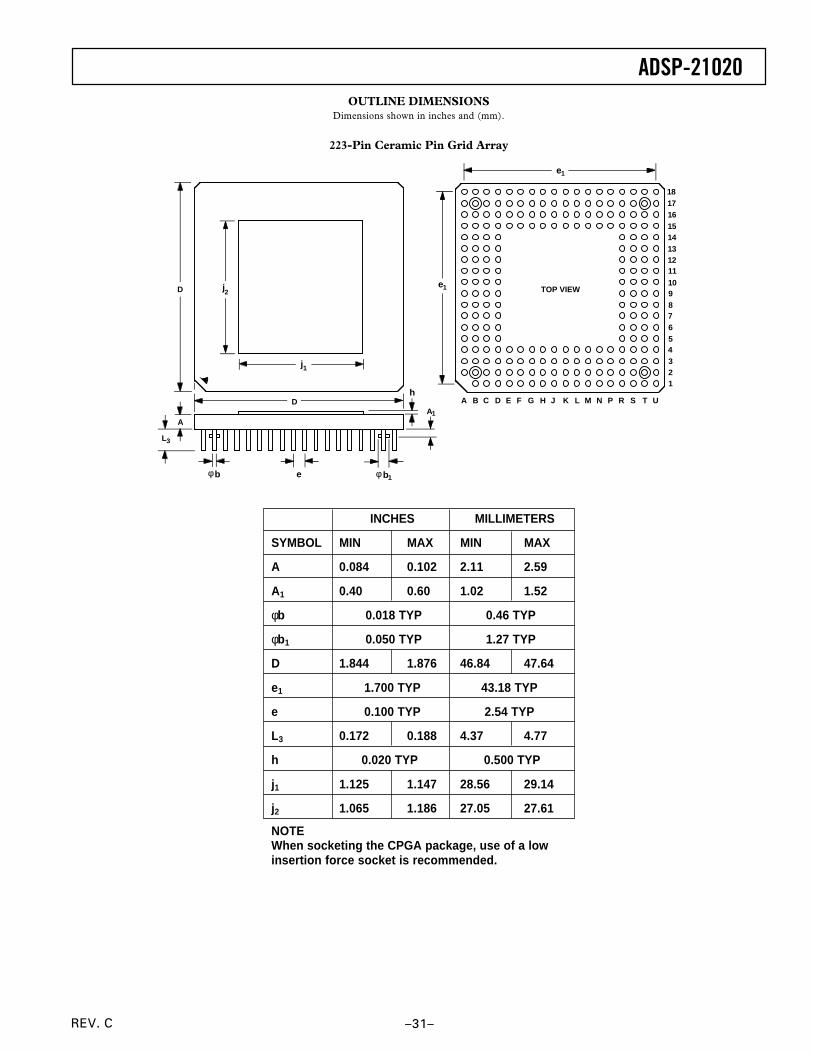
OUTLINE DIMENSIONSDimensions shown in inches and (mm).
223-Pin Ceramic Pin Grid Array
D
D
AA1
L3
b1φe
h
bφ
j1
j2
A B C D E F G H J K L M N P R S T U
123456789101112131415161718
TOP VIEWe1
e1
INCHES MILLIMETERS
SYMBOL MIN MAX MIN MAX
A 0.084 0.102 2.11 2.59
A1 0.40 0.60 1.02 1.52
φb 0.018 TYP 0.46 TYP
φb1 0.050 TYP 1.27 TYP
D 1.844 1.876 46.84 47.64
e1 1.700 TYP 43.18 TYP
e 0.100 TYP 2.54 TYP
L3 0.172 0.188 4.37 4.77
h 0.020 TYP 0.500 TYP
j1 1.125 1.147 28.56 29.14
j2 1.065 1.186 27.05 27.61
NOTEWhen socketing the CPGA package, use of a lowinsertion force socket is recommended.
ADSP-21020
REV. C–32–
C1
60
1c–5
–8
/94
PR
INT
ED
IN
U.S
.A.
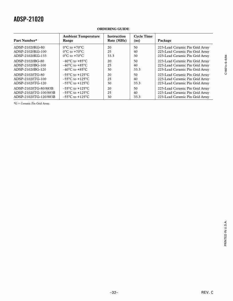
ORDERING GUIDE
Ambient Temperature Instruction Cycle TimePart Number* Range Rate (MHz) (ns) Package
ADSP-21020KG-80 0°C to +70°C 20 50 223-Lead Ceramic Pin Grid ArrayADSP-21020KG-100 0°C to +70°C 25 40 223-Lead Ceramic Pin Grid ArrayADSP-21020KG-133 0°C to +70°C 33.3 30 223-Lead Ceramic Pin Grid Array
ADSP-21020BG-80 –40°C to +85°C 20 50 223-Lead Ceramic Pin Grid ArrayADSP-21020BG-100 –40°C to +85°C 25 40 223-Lead Ceramic Pin Grid ArrayADSP-21020BG-120 –40°C to +85°C 30 33.3 223-Lead Ceramic Pin Grid Array
ADSP-21020TG-80 –55°C to +125°C 20 50 223-Lead Ceramic Pin Grid ArrayADSP-21020TG-100 –55°C to +125°C 25 40 223-Lead Ceramic Pin Grid ArrayADSP-21020TG-120 –55°C to +125°C 30 33.3 223-Lead Ceramic Pin Grid Array
ADSP-21020TG-80/883B –55°C to +125°C 20 50 223-Lead Ceramic Pin Grid ArrayADSP-21020TG-100/883B –55°C to +125°C 25 40 223-Lead Ceramic Pin Grid ArrayADSP-21020TG-120/883B –55°C to +125°C 30 33.3 223-Lead Ceramic Pin Grid Array
*G = Ceramic Pin Grid Array.