Embed Size (px)
Citation preview
A Three-Port Photovoltaic (PV) Micro-Inverter with Power Decoupling Capability
Souhib Harb, Haibing Hu, Nasser Kutkut, Issa Batarseh, Z. John Shen
Department of Electrical Engineering and Computer Science
University of Central Florida
Orlando, FL 32826
ABSTRACT: This paper presents a new micro-inverter topology that is intended for single-phase grid-connected PV systems. The features of the proposed topology are: (1) eliminating the double-frequency power ripple using small film capacitor; (2) improving the maximum-power-point tracking (MPPT) performance; (3) using long life-time film capacitors, which will improve the reliability of the inverter; and (4) requiring no additional circuitry to manage the transformer leakage energy.
Index terms- Power Decoupling, Single phase Inverter, Photovoltaic, Microinverter
I. INTRODUCTION Micro-Inverters connected to a single PV panel are
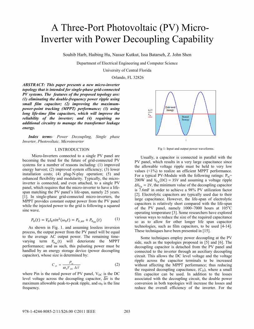
becoming the trend for the future of grid-connected PV systems for a number of reasons including: (1) improved energy harvest; (2) improved system efficiency; (3) lower installation costs; (4) plug-N-play operation; (5) and enhanced flexibility and modularity. Typically, the micro-inverter is connected, and even attached, to a single PV panel, which requires that the micro-inverter to have a life-span matching the PV panel’s life-span, namely 25 years. [1]. In single-phase grid-connected micro-inverters, the MPPT provides constant output power from the PV panel while the injected power to the grid is following a squared sine wave.
_ (1)
As shown in Fig. 1. and assuming lossless inversion process, the output power from the PV panel will be equal to the average AC output power. The remaining time-varying term P t will deteriorate the MPPT performance; and as such, this pulsating power must be handled by an energy storage device (power decoupling capacitor), whose size is determined by:
vVPCDC
inD ~
0 Δ=
ω (2)
where Pin is the rated power of PV panel, VDC is the DC level voltage across the decoupling capacitor, ∆v is the maximum allowable peak-to-peak ripple, and ω0 is the line frequency.
Usually, a capacitor is connected in parallel with the
PV panel, which results in a very large capacitance since the allowable voltage ripple must be held to very low values (<1%) to realize an efficient MPPT performance. For a typical PV-Module with the following ratings: Pin= 200W and VCD DC 35V and assuming a voltage ripple ∆VCD 2V, the minimum value of the decoupling capacitor is 7.6mF in order to achieve a 98% PV utilization factor [2]. Electrolytic capacitors are typically used due to their large capacitance. However, the life-span of electrolytic capacitors is relatively short compared with the life-span of the PV panel, namely 1000~7000 hours at 105oC operating temperature [3]. Some researchers have explored various ways to reduce the size of the required capacitance so as to allow for other longer life span capacitor technologies, such as film capacitors, to be used [4-14]. These techniques have been presented in [15].
Some techniques employ power decoupling at the PV side, such as the topologies proposed in [5] and [6]. The decoupling capacitor is detached from the PV panel and connected to the inverter through an auxiliary decoupling circuit. This allows the DC level voltage and the voltage ripple across the capacitor terminals to be increased without affecting the MPPT performance; thus reducing the required decoupling capacitance, (CD), where a small film capacitor can be used. In addition to the losses associated with the decoupling circuit, the double power conversion in both topologies will increase the losses and reduce the overall efficiency of the inverter. For the
Fig 1: Input and output power waveforms.
978-1-4244-8085-2/11/$26.00 ©2011 IEEE 203
topology in [5], a dissipative RCD clamp circuit is needed to handle the transformer leakage energy problem, which further increases the power losses. A modified version of the topology in [5] was proposed in [6]; where the leakage energy is stored in the decoupling capacitor through the decoupling circuit and no dissipative snubber circuit is needed. The decoupling circuit in [5] consists of one switch and one diode while in [6] four switches and two diodes are needed. Three port converters are proposed in recent years to interface different renewable sources [16].These topologies also can be modified to implement power decoupling in single-stage micro-inverter applications [17].In this paper, we propose a new topology that employs power decoupling at the PV side; where the transformer leakage energy is stored in the decoupling capacitor with minimal added components. More details will be given in next sections.
II. THE PROPOSED THREE-PORT MICRO INVERTER
The proposed topology is presented in Fig. 2. The power decoupling circuit consists of only one switch and two diodes in addition to the decoupling capacitor. The operation of this topology is divided into two main modes: (1) charging mode; (2) discharging mode. The decoupling capacitor will act as a secondary port. It will work as a load in the first mode and as a source in the second mode.
Grid
S1
S2
D1
D2
S4
S3
D3
D4
T
Cf
Lf
Cdc
CDPV
Fig 2: The proposed Three-Port Micro-Inverter.
III.MODE OF OPERATION The operation depends on the value of the output
power, )(0 tP . From Fig. 1, the circuit will be operating in mode-I (charging mode) when
inPtP <)(0. During this
mode, the extra energy will be stored in the decoupling capacitor. When
inPtP >)(0, the circuit will be operating in
mode-II (discharging mode). The decoupling capacitor will support the PV panel by discharging energy into the transformer and transferring the required power to the output (utility grid).
Mode-I
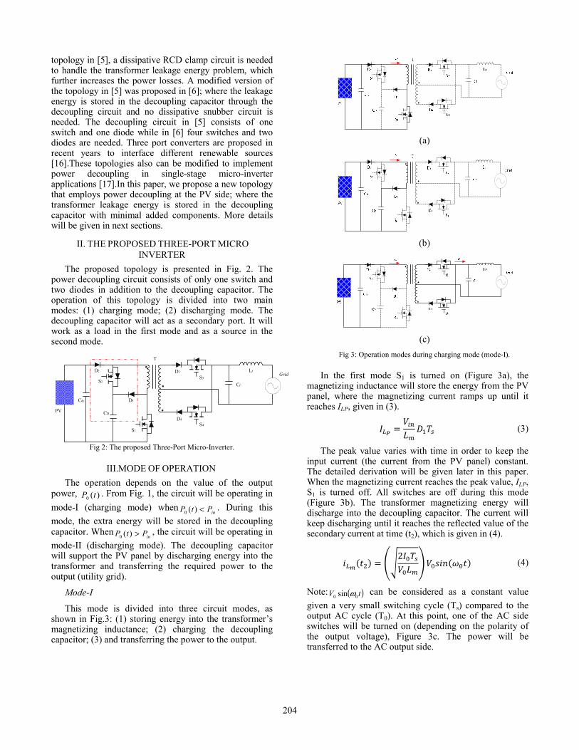
This mode is divided into three circuit modes, as shown in Fig.3: (1) storing energy into the transformer’s magnetizing inductance; (2) charging the decoupling capacitor; (3) and transferring the power to the output.
(a)
(b)
(c)
Fig 3: Operation modes during charging mode (mode-I).
In the first mode S1 is turned on (Figure 3a), the magnetizing inductance will store the energy from the PV panel, where the magnetizing current ramps up until it reaches ILP, given in (3).
(3)
The peak value varies with time in order to keep the input current (the current from the PV panel) constant. The detailed derivation will be given later in this paper. When the magnetizing current reaches the peak value, ILP, S1 is turned off. All switches are off during this mode (Figure 3b). The transformer magnetizing energy will discharge into the decoupling capacitor. The current will keep discharging until it reaches the reflected value of the secondary current at time (t2), which is given in (4). 2
(4)
Note: ( )tV 00 sin ω can be considered as a constant value given a very small switching cycle (Ts) compared to the output AC cycle (T0). At this point, one of the AC side switches will be turned on (depending on the polarity of the output voltage), Figure 3c. The power will be transferred to the AC output side.
204
Using the power equation, ILP can be derived as 12 12 (5)
It can be found that
(6)
(7)
Substituting (6) and (7) in (5), then:
2 1 (8)
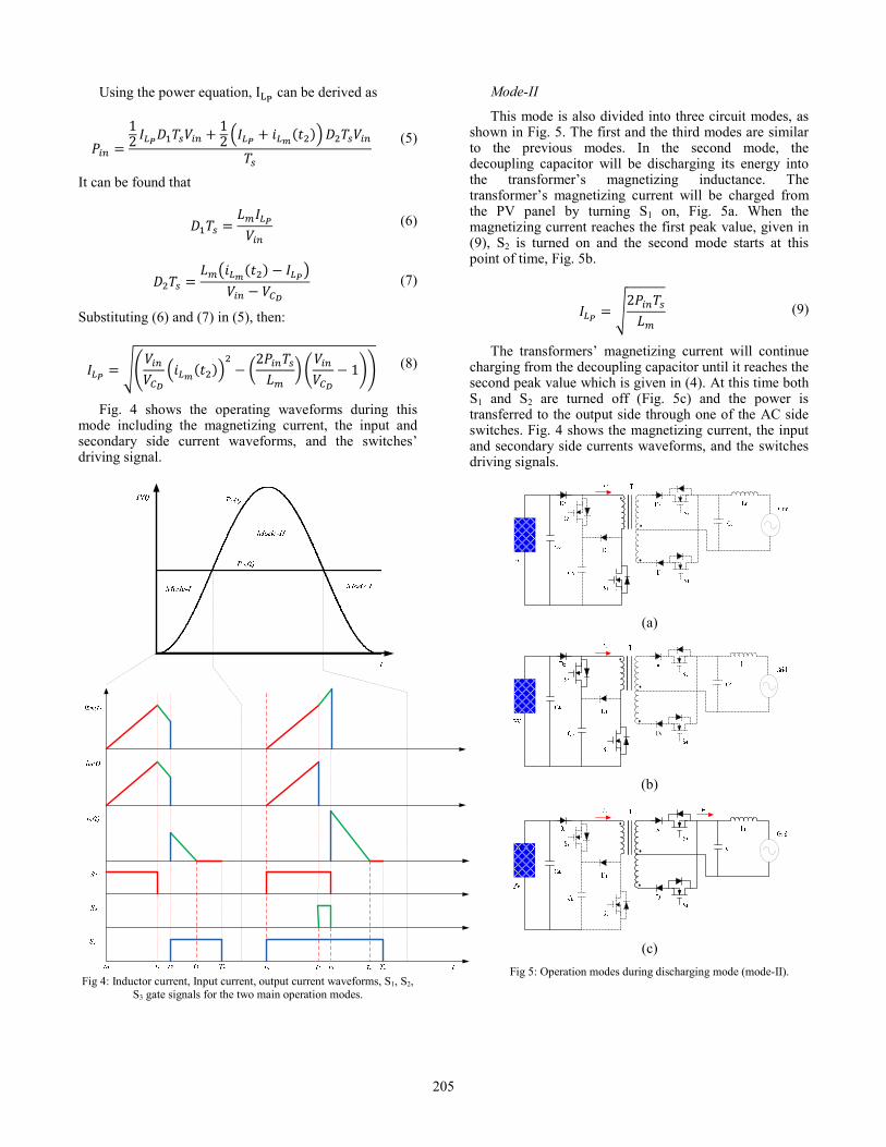
Fig. 4 shows the operating waveforms during this mode including the magnetizing current, the input and secondary side current waveforms, and the switches’ driving signal.
Fig 4: Inductor current, Input current, output current waveforms, S1, S2, S3 gate signals for the two main operation modes.
Mode-II
This mode is also divided into three circuit modes, as shown in Fig. 5. The first and the third modes are similar to the previous modes. In the second mode, the decoupling capacitor will be discharging its energy into the transformer’s magnetizing inductance. The transformer’s magnetizing current will be charged from the PV panel by turning S1 on, Fig. 5a. When the magnetizing current reaches the first peak value, given in (9), S2 is turned on and the second mode starts at this point of time, Fig. 5b.
2 (9)
The transformers’ magnetizing current will continue charging from the decoupling capacitor until it reaches the second peak value which is given in (4). At this time both S1 and S2 are turned off (Fig. 5c) and the power is transferred to the output side through one of the AC side switches. Fig. 4 shows the magnetizing current, the input and secondary side currents waveforms, and the switches driving signals.
(a)
(b)
(c)
Fig 5: Operation modes during discharging mode (mode-II).
205
It can be noticed from the operation modes that the leakage energy is stored in the decoupling capacitor without using any additional circuit. This is one of the advantages of the proposed topology. In [5], this leakage energy will cause a spike on the decoupling switch at turn off time when the energy is transferred to the AC side. The modified topology in [6] solved this problem by storing the leakage energy in the decoupling capacitor through the flyback diodes. The advantages of the proposed topology over the previous topologies in [5] [6] can be summarized as follows:
1. No double power conversion, which results in reduced power losses.
2. The transformer leakage energy is stored in the decoupling capacitor through D1. This means that there is no need for extra dissipative clamp circuits. Again, this will reduce the power losses.
3. Fewer components are used in the decoupling circuit, only one switch and two diodes, unlike the topology in [6], where four switches and two diodes are required.
IV. THE DECOUPLING CAPACITOR (CD) The formula that governs the decoupling capacitor
(CD) value will be derived in this section. During sub-mode-3 in both main modes, the energy that has been stored in the magnetizing inductance will be transferred to the secondary side. Wherefore, the voltage across the decoupling capacitor must be greater than the stress voltage across S1, which is given in (10).
2 (10)
Then, the minimum voltage across CD must satisfy the following condition (11).
(11)
But, the minimum voltage across CD is given in (12). ∆2 (12)
Using (11) and (12), the relationship in (13) can be derived. By choosing a certain DC-level across the CD, the maximum allowed voltage ripple can be found.
∆ 2 (13)
It is worth to mention that when we choose the DC-level voltage across the decoupling capacitor we should take in the consideration the stresses on the power devices at the input side (S1, S2, D1, and D2). Now, for a certain system parameters, we can choose the appropriate value for the decoupling capacitor. Consider a 100W system with 35V as an input voltage with a grid voltage and
frequency of 110Vrms and 60Hz, respectively. Let us choose a DC-level across the decoupling capacitor of 120V. Then the ripple should be less than 107V. Assuming a value of 100V and using (2), 22.1µF of decoupling capacitance is needed.
V. SIMULATION RESULTS The PSIM software is used to simulate the proposed
topology. Table 1 lists the components’ values that were used in the simulation.
Table 1: Proposed topology component values.
Fig. 6 shows the simulation results. In Fig. 6, the magnetizing inductance, input, and secondary currents waveforms for one complete grid cycle are shown.
Magnetizing inductance current, iLm(t)
Input current, iin(t)
Secondary side current, i2(t)
Fig 6: Simulation results of the proposed topology.
Fig. 7 and Fig. 8 show an expanded view of the circuit operation in mode-I and mode-II, respectively.
Fig 7: Expanded view for the simulation results for mode-I.
Input Power (Pin) 100 W Input Voltage (Vin) 35 V Magnetizing Inductance (Lm) 7µH Turns Ration (N) 5
Decoupling Capacitance (CD) 40µF Cf 1µF
Output Resistor (Ro) 120Ω Lf 1mH
206
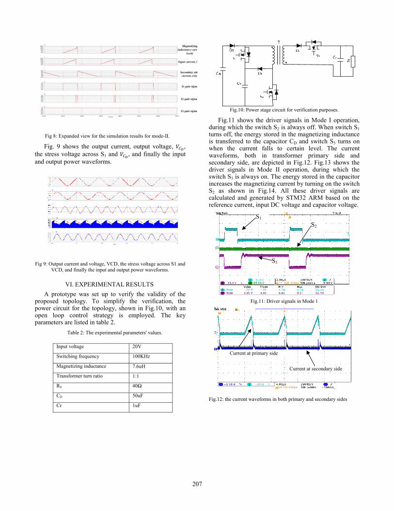
Fig 8: Expanded view for the simulation results for mode-II.
Fig. 9 shows the output current, output voltage, , the stress voltage across S1 and , and finally the input and output power waveforms.
Fig 9: Output current and voltage, VCD, the stress voltage across S1 and
VCD, and finally the input and output power waveforms.
VI. EXPERIMENTAL RESULTS A prototype was set up to verify the validity of the
proposed topology. To simplify the verification, the power circuit for the topology, shown in Fig.10, with an open loop control strategy is employed. The key parameters are listed in table 2.
Table 2: The experimental parameters' values.
Input voltage 20V
Switching frequency 100KHz
Magnetizing inductance 7.6uH
Transformer turn ratio 1:1
R0 40Ω
CD 50uF
Cr 1uF
Fig.10: Power stage circuit for verification purposes.
Fig.11 shows the driver signals in Mode I operation, during which the switch S2 is always off. When switch S1 turns off, the energy stored in the magnetizing inductance is transferred to the capacitor CD and switch S3 turns on when the current falls to certain level. The current waveforms, both in transformer primary side and secondary side, are depicted in Fig.12. Fig.13 shows the driver signals in Mode II operation, during which the switch S3 is always on. The energy stored in the capacitor increases the magnetizing current by turning on the switch S2 as shown in Fig.14. All these driver signals are calculated and generated by STM32 ARM based on the reference current, input DC voltage and capacitor voltage.
Fig.11: Driver signals in Mode 1
Fig.12: the current waveforms in both primary and secondary sides
S1
S3
S2
Current at primary side
Current at secondary side
207
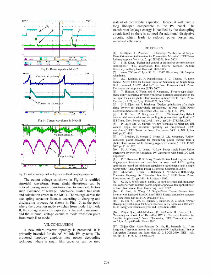
Fig 13: Driver signals in Mode 2
Fig.14: Current waveforms in Mode II
Fig. 15: output voltage and voltage across the decoupling capacitor
The output voltage as shown in Fig.15 is rectified sinsoidal waveform. Some slight distortions can be noticed during mode transitions due to nonideal factors such existance of leakage inductance, switch transients and calculation errors in the MCU. The voltage across the decoupling capacitor fluctates according to charging and discharging process. As shown in Fig. 15, at the point where the operation mode switches from mode I to mode II, the voltage across the capacitor is charged to maximum and the minimal voltage occurs at mode transition point from mode II to mode I.
VII. CONCLUSION A new micro-inverter topology is presented. It is
primarily intended for the AC-Module PV systems. The proposed topology employs new power decoupling technique where a small film capacitor can be used
instead of electrolytic capacitor. Hence, it will have a long life-span comparable to the PV panel. The transformer leakage energy is handled by the decoupling circuit itself so there is no need for additional dissipative circuits; which leads to reduced power losses and improved efficiency.
REFERENCES [1] S.B.Kjaer, J.H.Pedersen, F. Blaabjerg. “A Review of Single-Phase Grid-connected Inverters for Photovoltaic Modules”. IEEE Trans. Industry Applica. Vol.41 no.5, pp.1292-1306, Sept. 2005. [2] S. B. Kjaer, “Design and control of an inverter for photovoltaic applications,” Ph.D. dissertation, Inst. Energy Technol., Aalborg University, Aalborg East, Denmark, 2004/2005. [3] www.CDE.com// Type 381EL 1050C Ultra-Long Lift Snap-In, Aluminum. [4] A.C. Kyritsis, N. P. Papanikolaou, E. C. Tatakis. “A novel Parallel Active Filter for Current Pulsation Smoothing on Single Stage Grid connected AC-PV Modules”, in Proc. European Conf. Power Electronics and Applications (EPE), 2007. [5] T. Shimizu, K. Wada, and N. Nakamura, “Flyback-type single-phase utility interactive inverter with power pulsation decoupling on the dc input for an ac photovoltaic module system,” IEEE Trans. Power Electron., vol. 21, no. 5, pp. 1264–1272, Sep. 2006. [6] S. B. Kjaer and F. Blaabjerg, "Design optimization of a single phase inverter for photovoltaic applications," in Proc. IEEE Power Electronics Specialists Conference, 2003, vol. 3, pp. 1183-1190. [7] G. H. Tan, J. Z. Wang, and Y. C. Ji, “Soft-switching flyback inverter with enhanced power decoupling for photovoltaic applications,” IET Trans. Elect. Power Appl., vol. 1, no. 2, pp. 264–274, Mar. 2007. [8] P. Enjeti and W. Shireen, “A new technique to reject DC link voltage ripple for inverters operating on programmed PWM waveforms,” IEEE Trans. on Power Electronics, VOL. 7, NO. 1, Jan. 1992.pp.171-180. [9] T. Brekken. N. Mohan, C. Henze, & L.R. Moumneh, "Utility-connected power converter for maximizing power transfer from a photovoltaic source while drawing ripple-free current," IEEE PESC, 2002.pp.1518-1522. [10] N. A. Ninad, L. Lopes, “A Low Power single-Phase Utility Interactive Inverter for Residential PV Generation with Small DC Link Capacitor” [11] P. T. Krein and R. S. Balog, "Cost-effective hundred-year life for single-phase inverters and rectifiers in solar and LED lighting applications based on minimum capacitance requirements and a ripple power port," IEEE Applied Power Electronics Conference, 2009. [12] Al-Atrash, H.; Tian, F.; Batarseh, I., “Tri-Modal Half-Bridge Converter Topology for Three-Port Interface,” IEEE Trans. Power Electronics, vol. 22, pp. 341 - 345, January 2007. [13] Q. Li, P. Wolfs, and S. Senini, “A hard switched high frequency link converter with constant power output for photovoltaic applications,” in Proc. Australasian Univ. Power Eng. Conf., 2002. [14] C. Bush, B. Wang. “A Single-Phase Current Source Solar Inverter with Reduced-Size DC Link” IEEE Energy conversion congress and Exposition, San Jose,CA, 2009,pp.54-59. [15] H. Hu, S. Harb, N. Kutkut, I. Batarseh, Z. J. Shen, “Power Decoupling Techniques for Micro-inverters in PV Systems-a Review”, IEEE Energy conversion congress and Exposition, 2010.
[16] Zhijun Qian; Abdel-Rahman, O.; Al-Atrash, H.; Batarseh, I.; , "Modeling and Control of Three-Port DC/DC Converter Interface for Satellite Applications," Power Electronics, IEEE Transactions on , vol.25, no.3, pp.637-649, March 2010
[17] Zhijun Qian; Abdel-Rahman, O.; Hu, H.; Batarseh, I.; , " An Integrated Three-port Inverter for Stand-alone PV Applications," Energy Conversion Congress and Exposition, 2010. ECCE 2010. IEEE , vol., no., pp.1471-1478, 12-16 Sept. 2010
S1 S2 S3
Output voltage
Voltage across Cd
Current at primary id
Current at secondaryid
208

![A Performance Model for Photovoltaic Modules with ...€¦ · of existing models [1-4]. Some manufacturers are fully integrating a microinverter into a PV module, combining the separate](https://img.pdfslide.us/doc/110x75/5f7666e4b7ef92542b438c2e/a-performance-model-for-photovoltaic-modules-with-of-existing-models-1-4.jpg)