Embed Size (px)
Citation preview

LUND UNIVERSITY
PO Box 117221 00 Lund+46 46-222 00 00
A 2.4 GHz CMOS power amplifier using internal frequency doubling
Cijvat, Pieternella; Troedsson, Niklas; Sjöland, Henrik
Published in:2005 IEEE International Symposium On Circuits And Systems (Iscas), Vols 1-6, Conference Proceedings
DOI:10.1109/ISCAS.2005.1465179
2005
Link to publication
Citation for published version (APA):Cijvat, P., Troedsson, N., & Sjöland, H. (2005). A 2.4 GHz CMOS power amplifier using internal frequencydoubling. In 2005 IEEE International Symposium On Circuits And Systems (Iscas), Vols 1-6, ConferenceProceedings (pp. 2683-2686). IEEE - Institute of Electrical and Electronics Engineers Inc..https://doi.org/10.1109/ISCAS.2005.1465179
Total number of authors:3
General rightsUnless other specific re-use rights are stated the following general rights apply:Copyright and moral rights for the publications made accessible in the public portal are retained by the authorsand/or other copyright owners and it is a condition of accessing publications that users recognise and abide by thelegal requirements associated with these rights. • Users may download and print one copy of any publication from the public portal for the purpose of private studyor research. • You may not further distribute the material or use it for any profit-making activity or commercial gain • You may freely distribute the URL identifying the publication in the public portal
Read more about Creative commons licenses: https://creativecommons.org/licenses/Take down policyIf you believe that this document breaches copyright please contact us providing details, and we will removeaccess to the work immediately and investigate your claim.
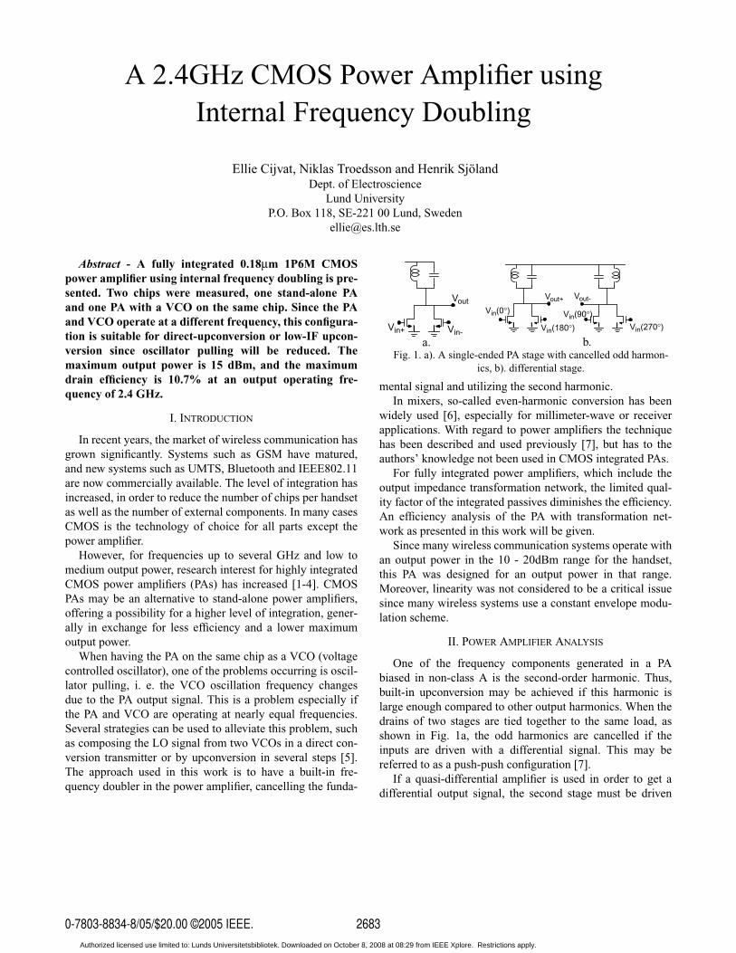
Abstract - A fully integrated 0.18µm 1P6M CMOSpower amplifier using internal frequency doubling is pre-sented. Two chips were measured, one stand-alone PAand one PA with a VCO on the same chip. Since the PAand VCO operate at a different frequency, this configura-tion is suitable for direct-upconversion or low-IF upcon-version since oscillator pulling will be reduced. Themaximum output power is 15 dBm, and the maximumdrain efficiency is 10.7% at an output operating fre-quency of 2.4 GHz.
I. INTRODUCTION
In recent years, the market of wireless communication hasgrown significantly. Systems such as GSM have matured,and new systems such as UMTS, Bluetooth and IEEE802.11are now commercially available. The level of integration hasincreased, in order to reduce the number of chips per handsetas well as the number of external components. In many casesCMOS is the technology of choice for all parts except thepower amplifier.
However, for frequencies up to several GHz and low tomedium output power, research interest for highly integratedCMOS power amplifiers (PAs) has increased [1-4]. CMOSPAs may be an alternative to stand-alone power amplifiers,offering a possibility for a higher level of integration, gener-ally in exchange for less efficiency and a lower maximumoutput power.
When having the PA on the same chip as a VCO (voltagecontrolled oscillator), one of the problems occurring is oscil-lator pulling, i. e. the VCO oscillation frequency changesdue to the PA output signal. This is a problem especially ifthe PA and VCO are operating at nearly equal frequencies.Several strategies can be used to alleviate this problem, suchas composing the LO signal from two VCOs in a direct con-version transmitter or by upconversion in several steps [5].The approach used in this work is to have a built-in fre-quency doubler in the power amplifier, cancelling the funda-
mental signal and utilizing the second harmonic.In mixers, so-called even-harmonic conversion has been
widely used [6], especially for millimeter-wave or receiverapplications. With regard to power amplifiers the techniquehas been described and used previously [7], but has to theauthors’ knowledge not been used in CMOS integrated PAs.
For fully integrated power amplifiers, which include theoutput impedance transformation network, the limited qual-ity factor of the integrated passives diminishes the efficiency.An efficiency analysis of the PA with transformation net-work as presented in this work will be given.
Since many wireless communication systems operate withan output power in the 10 - 20dBm range for the handset,this PA was designed for an output power in that range.Moreover, linearity was not considered to be a critical issuesince many wireless systems use a constant envelope modu-lation scheme.
II. POWER AMPLIFIER ANALYSIS
One of the frequency components generated in a PAbiased in non-class A is the second-order harmonic. Thus,built-in upconversion may be achieved if this harmonic islarge enough compared to other output harmonics. When thedrains of two stages are tied together to the same load, asshown in Fig. 1a, the odd harmonics are cancelled if theinputs are driven with a differential signal. This may bereferred to as a push-push configuration [7].
If a quasi-differential amplifier is used in order to get adifferential output signal, the second stage must be driven
Fig. 1. a). A single-ended PA stage with cancelled odd harmon-ics, b). differential stage.
Vin-Vin+
Vout
Vin(90°)
Vin(180°)
Vin(0°)
Vin(270°)
Vout+ Vout-
a. b.
A 2.4GHz CMOS Power Amplifier usingInternal Frequency Doubling
Ellie Cijvat, Niklas Troedsson and Henrik SjölandDept. of Electroscience
Lund UniversityP.O. Box 118, SE-221 00 Lund, Sweden
26830-7803-8834-8/05/$20.00 ©2005 IEEE.Authorized licensed use limited to: Lunds Universitetsbibliotek. Downloaded on October 8, 2008 at 08:29 from IEEE Xplore. Restrictions apply.

with a 90° phase shift relative to the first stage, as shown inFig. 1b. Quadrature signals are thus needed to drive the dif-ferential PA.
Ideal PA response
Assuming that the output stage of the PA can be modeledas an ideal current source with a maximum voltage swing of2VDD at the drain node, the DC, fundamental and 2nd orderresponse of the PA depend on the conduction angle α orclass in which the PA is biased [8].
For this ideal PA both the fundamental and second orderresponses (output currents normalized to the maximum out-put current Imax), as well as the efficiencies η1 and η2 aredepicted in Fig. 2, as a function of the conduction angle α.So far it is assumed that the PA does not have a so-calledknee voltage Vknee [8], that only relevant harmonics are seenat the output, and that the load impedance is always opti-mized for maximum voltage swing (2VDD) with maximumcurrent swing Imax.
The impedance transformation network.
The MOSFET DC current is supplied through inductorL1. The section formed by Lbw (the output bondwire induct-ance) and C3 in the network shown in Fig. 3 can be seen as alow-pass up-transformation L-section, and the section C1and C2 as a down-transformation stage. In theory this pro-vides us with enough degrees of freedom to ensure sufficientbandwidth while being able to freely choose the transforma-tion ratio. However, both parasitics and size limitations for
integrated passive components limit the impedance transfor-mation ratio Parasitic capacitances from the pad may beincluded in C3, while parasitic capacitances at the drain areincluded in C1. For the PA with internal frequency doublingthe network must be tuned so that the desired impedancetransformation is achieved at twice the PA input frequency.In the next section we will look more into non-idealities ofthe transformation network.
III. IMPLEMENTATION
The quasi-differential PA as described in the previous sec-tion was implemented in a 0.18µm 1P6M CMOS technologywith the option of 3.3V supply. Since we aimed at outputpowers of 15 - 20 dBm, this supply voltage was chosen, andthus non-minimum length MOSFETs were used in the finalstage. One test chip included a passive polyphase filter, apre-amplifier and the PA, while a second test chip includedboth a quadrature VCO and the PA. The block diagrams areshown in Fig. 4.
The goal of the circuit in Fig. 4a was to test the concept ofinternal frequency doubling, as well as the output power andefficiency in the final PA stage. The polyphase network pro-vides the driving stage with I- and Q- signals, but has a sig-nificant signal loss. The PA schematic is shown in Fig. 5.
For the VCO core in the circuit of Fig. 6 PMOSFETswere used, so that the VCO output voltage swings aroundground, the desired bias voltage of the PA input. The two
0 1 2 3 4 5 6 70
0.1
0.2
0.3
0.4
0.5
0.6
0.7
alfa
0 1 2 3 4 5 6 70
10
20
30
40
50
60
70
80
90
100
alfa
Fig. 2. a). Ideal normalized DC, fundamental and second orderoutput current as function of the conduction angle α, b). drain
efficiency for the fundamental and second-order output.
a. b.
effic
ienc
y [%
]
η1
η2
Io/Im
ax
I1
Idc
I2
α0 71 2 3 4 5 6
100
0
50
α0 71 2 3 4 5 6
.7
0
.1
.2
.3
.4
.5
.6
Fig. 3. a). A PA with transformation network (shaded area), b).an ideal model.
RLRopt
TVDD
a. b.
Lbw
C3
C2
C1L1
i+
i-o+o-
i+
i-o+o-
Fig. 4. Block diagrams, a). stand-alone PA, b). PA with VCO.
Vo+ Vo-Vi+ Vi-
a.
b.
Poly-Phase
Network
PA 100Ω
PA 100Ω
VCO
Fig. 5. Simplified schematic of the PA.
Vout+ Vout-
2684Authorized licensed use limited to: Lunds Universitetsbibliotek. Downloaded on October 8, 2008 at 08:29 from IEEE Xplore. Restrictions apply.

blocks can then be connected without buffer or couplingcapacitor; a disadvantage is that this more or less fixes thePA input bias voltage, while an advantage is that no signaldegradation will take place between the VCO and PA. Theswitched tuning of the varactor as shown in Fig. 6 has beendescribed earlier [9].
Non-idealities of the PA implementation
One of the most crucial non-idealities in any PA imple-mentation is the knee voltage Vknee, i.e. the minimum drainvoltage necessary to have the PA operating as an amplifier.Vknee will reduce the maximum voltage swing and thus themaximum output power, as well as the efficiency [8].
The integrated passives that make up the impedance trans-formation network, including “RF choke” inductor, all havea limited quality factor Q. The inductors are differential, sav-ing area and giving a higher Q factor compared to single-ended inductors with similar inductance value. The inductordesign and modeling was done in-house [10]. The transfor-mation network was designed to transorm the 50 Ω antennaimpedance to 90 Ω at the frequency of operation.
For the transformation network of Fig. 3 with suitable
capacitor and inductor values, including a Q factor of 12 forthe inductor L1, MATLAB simulations showed that the effi-ciency of the transformation network is about 75%, i.e. thepower loss from drain to output will be about 1.2dB. Moreo-ver, in a real impedance transformation network also capaci-tor non-idealities and interconnect parasitics will causepower losses.
IV. RESULTS
Both the stand-alone PA and the PA with VCO were pack-aged in an LCC package and attached to a PCB. In Fig. 7 thechip micrograph of the PA with VCO is shown. Parasiticsrelated to the bondwires, package and board were estimatedand taken into account in simulations.
The stand-alone PA
The purpose of this circuit was to verify that the internalfrequency doubling worked, and to characterize the finalstage. Due to the on-chip polyphase network used to gener-ate the quadrature phases the gain is low. In the measure-ments the circuit was therefore preceded by a Mini-Circuitsamplifier. In Fig. 8 measurement results for the stand-alonePA are shown.
The PA with VCO
In Fig. 9 the output power and efficiency as function ofVdd,vco is shown. Increasing Vdd,vco is equivalent to increas-ing the input power of the PA stage.
Fig. 6. Schematic of the VCO, including the varactor with con-tinuous and discrete tuning.
-+vctrl
Vi+ Vi-Varactor VaractorVq- Vq+
Fig. 7. A chip micrograph of the PA with VCO.
PA
VCO
−15 −10 −5 0−25
−20
−15
−10
−5
0
5
10
15
Pin [dBm]
Pout [dBm]
Stand−alone PA; VddDR=3.3
Vdd,PA=3
Vdd,PA=3.3
−15 −10 −5 00
2
4
6
8
10
12
Pin [dBm]
efficiency [%]
Stand−alone PA; VddDR=3.3
Vdd,PA=3.3
Vdd,PA=3
Fig. 8. Measured results for the stand-alone PA for Vdd,pa=3.3and 3 V, a). output power, b). drain efficiency.
a. b.Pin [dBm]
=Vdd,PA=3=Vdd,PA=3.3
0-15 -10 -5 0-15 -10 -5
Pou
t [dB
m]
-25
15
5
-5
-15
effic
ienc
y [%
]
0
12
8
4
Pin [dBm]
Vdd,PA=3
Vdd,PA=3.3
2.2 2.4 2.6 2.8 3 3.2 3.4 3.6−35
−30
−25
−20
−15
−10
−5
0
5
10
VDD,vco [V]
Pout [dBm]
PA + VCO; VddPA=3.3
2.2 2.4 2.6 2.8 3 3.2 3.4 3.60
0.5
1
1.5
2
2.5
3
3.5
4
4.5
5
VDD,vco [V]
efficiency [%]
PA + VCO; VddPA=3.3
Fig. 9. Measured results for the PA with VCO as a function ofVdd,vco for two different VCO control words, a). output power,
b). drain efficiency.
(1111)
(1101)
(1111)
(1101)
a. b.Vdd,VCO [V]
2.2 2.6 3 3.4Vdd,VCO [V]
2.2 2.6 3 3.4
Pou
t [dB
m]
10
-5
-20
-35
effic
ienc
y [%
]
0
5
2.5
2685Authorized licensed use limited to: Lunds Universitetsbibliotek. Downloaded on October 8, 2008 at 08:29 from IEEE Xplore. Restrictions apply.

The VCO used in this circuit was not optimized for thepurpose. Therefore, it could not drive the PA sufficientlywhich had a negative impact on the efficiency and outputpower. For equal VCO supply voltage, the driving power washigher when using the control word (1111) compared tousing (1101), thus giving a larger PA output power and a bet-ter PA drain efficiency. Moreover, the oscillation frequencywas not in agreement with the optimum PA operating fre-quency. Off-chip components were used to tune the PA to theright frequency.
Fig. 10 shows the output power as function of Vdd,PA,illustrating the knee effect, and the drain efficiency. Themaximum efficiency occurs for relatively low supply volt-ages; this illustrates the fact that for equal driving power, thePA with low supply voltage has a clipped output voltagewaveform, which may be beneficial for the efficiency [8].For even lower supply voltages (Vdd,PA < 0.6 V, see Fig. 10b)the MOSFET will be in triode and thus have a lower gm,resulting in a decreasing efficiency.
Measurements of both circuits showed that the gain ineach block is less than expected from simulations. This maybe due to a lower transistor gm or lower inductor Q value.This has a large impact on the total gain, but also on the effi-ciency of the PA and power consumption of the VCO. InTable 1 the measurement results are summarized.
As was shown in Section II, the efficiency and the outputpower are degraded since the 2nd harmonic is taken insteadof the fundamental.
V. CONCLUSIONS
A fully integrated class-C power amplifier with internalfrequency doubler has been designed and measured. A0.18µm 1P6M CMOS technology was used. The circuit is
suitable for a direct-conversion or low-IF transmitter, sincethe PA and VCO do not operate at the same frequency. Thus,VCO pulling will be reduced. The maximum output power is15 dBm, with a maximum drain efficiency of 10.7%. Theconcept of internal frequency doubling was tested both in astand-alone PA and a PA with VCO on the same chip.
REFERENCES
[1]. M. Rofougaran, A. Rofougaran, C. Ølgaard, and A.A.Abidi, “A 900 MHz CMOS RF power amplifier withprogrammable output”, in 1994 Symposium on VLSICircuits Digest, pp. 133-134, June 1994.
[2]. I. Aoki, S.D. Kee, D.B. Rutledge, and A. Hajimiri,“Fully integrated CMOS power amplifier design usingthe distributed active-transformer architecture”, IEEEJournal of Solid-State Circuits, Vol. 37, no.3, pp. 371-383, March 2002.
[3]. Y.J.E. Chen, M. Hamai, D. Heo, A. Sutono, S. Yoo, andJ. Laskar, “RF power amplifier integration in CMOStechnology”, in 2000 IEEE Microwave Symposium(MTT-S) Digest, pp. 545-548, May 2001.
[4]. R. Gupta, B.M. Ballweber, and D.J. Allstot, “Designand optimization of CMOS RF power amplifiers”, IEEEJournal of Solid-State Circuits, Vol. 36 no. 2, pp. 166-175, February 2001.
[5]. B. Razavi, RF Microelectronics. Prentice Hall PTR,Upper Saddle River, NJ, 1998.
[6]. M. Cohn, J.E. Degenford and B.A. Newman, “Har-monic mixing with an antiparallel diode pair”, IEEETrans. on Microwave Theory and Techniques, Vol.MTT-23 no. 8, pp. 667-673, August 1975.
[7]. R. Martin and F. Ali, “A Ku-band oscillator subsystemusing a broadband GaAs MMIC push-pull amplifier/doubler”, IEEE Microwave and Guided Wave Letters,Vol. 1 no. 11, pp. 348-350, November 1991.
[8]. S.C. Cripps, “RF power amplifiers for wireless commu-nication”. Artech House, Norwood, MA, USA, 1999.
[9]. H. Sjöland, “Improved switched tuning of differentialCMOS VCOs”, IEEE Trans. on Circuits and SystemsII: Analog and Digital Signal Processing, Vol. 49 no. 5,pp. 352-355, May 2002.
[10].N. Troedsson and H. Sjöland, “A distributed capaci-tance analysis of co-planar inductors for a CMOSQVCO with varactor tuned buffer stage”, Analog Inte-grated Circuits and Signal Processing, Vol. 42 no. 1,pp. 7-19, January 2005.
TABLE 1: SUMMARY OF MEASUREMENT RESULTS
maximum PA output power 15 dBm
maximum PA drain efficiency 10.7%
active area: stand-alone PAVCO + PA
1.44 mm2
2.25 mm2
0 0.5 1 1.5 2 2.5 3 3.5−25
−20
−15
−10
−5
0
5
10
Vdd,PA [V]
Pout [dBm]
PA + VCO; Vdd,vco=3.3
0 0.5 1 1.5 2 2.5 3 3.50
1
2
3
4
5
6
7
8
9
10
Vdd,PA [V]
efficiency [%]
PA + VCO; Vdd,vco=3.3
Fig. 10. Results for varying Vdd,PA, a). output power, b). drainefficiency.
a. b.Vdd,PA [V]
0 1 2 3Vdd,PA [V]
0 1 2 3
effic
ienc
y [%
]
10
0
5Pou
t [dB
m]
10
0
-10
-20
2686Authorized licensed use limited to: Lunds Universitetsbibliotek. Downloaded on October 8, 2008 at 08:29 from IEEE Xplore. Restrictions apply.


![Operational Transconductance Amplifier (OTA) in 45nm CMOS · Amplifier (OTA) in 45nm CMOS YOUNGSEOK LEE ... Design of Analog CMOS Integrated Circuits. McGraw-Hill, 2002. [2] B. Ahuja,](https://img.pdfslide.us/doc/110x75/5fbfc7035b7a87264a188ff5/operational-transconductance-amplifier-ota-in-45nm-cmos-amplifier-ota-in-45nm.jpg)

![EECS 522 RF Power Amplifier with Cartesian Feedback · [5] D. Chowdhury; et al, “A 2.4GHz mixed signal polar power amplifier with low‐power integrated filtering in 65nm CMOS,”](https://img.pdfslide.us/doc/110x75/605954abc5036c62b2623d26/eecs-522-rf-power-amplifier-with-cartesian-5-d-chowdhury-et-al-aoea-24ghz.jpg)