Embed Size (px)
Citation preview
Microelectronics Journal 43 (2012) 687–696
Contents lists available at SciVerse ScienceDirect
Microelectronics Journal
0026-26
http://d
n Corr
E-m
klee84@
journal homepage: www.elsevier.com/locate/mejo
A 20 Gb/s triple-mode (PAM-2, PAM-4, and duobinary) transmitter
Byungho Min n, Keytaek Lee, Samuel Palermo
Department of Electrical and Computer Engineering, Texas A&M University, College Station, Texas 77843, United States
a r t i c l e i n f o
Article history:
Received 31 October 2011
Received in revised form
2 March 2012
Accepted 14 May 2012Available online 14 June 2012
Keywords:
Backplane transceiver
Bit-error rate (BER)
Duobinary
Feed-forward equalization (FFE)
I/O link
Inter-symbol interference (ISI)
Link analysis tools
Pulse-amplitude modulation (PAM)
Statistical signaling analysis
92/$ - see front matter & 2012 Elsevier Ltd. A
x.doi.org/10.1016/j.mejo.2012.05.009
esponding author. Tel.: þ1 979 422 6990.
ail addresses: [email protected], bhmin09
neo.tamu.edu (K. Lee), [email protected]
a b s t r a c t
Increasing data rates over electrical channels with significant frequency-dependent loss is difficult due
to excessive inter-symbol interference (ISI). In order to achieve sufficient link margins at high rates, I/O
system designers implement equalization in the transmitters and are motivated to consider more
spectrally-efficient modulation formats relative to the common PAM-2 scheme, such as PAM-4 and
duobinary. This paper reviews when to consider PAM-4 and duobinary formats, as the modulation
scheme which yields the highest system margins at a given data rate is a function of the channel loss
profile, and presents a 20 Gb/s triple-mode transmitter capable of efficiently implementing these three
modulation schemes and three-tap feed-forward equalization. A statistical link modeling tool, which
models ISI, crosstalk, random noise, and timing jitter, is developed to compare the three common
modulation formats operating on electrical backplane channel models. In order to improve duobinary
modulation efficiency, a low-power quarter-rate duobinary precoder circuit is proposed which provides
significant timing margin improvement relative to full-rate precoders. Simulation results of the
proposed transmitter in a 90 nm CMOS technology compare operation with the different modulation
schemes over three backplane channels with different loss profiles.
& 2012 Elsevier Ltd. All rights reserved.
1. Introduction
High-performance computing applications require I/O datarates to scale well past 10 Gb/s to meet the demand of futuresystems. However, inter-chip communication at high data ratesover standard electrical channels is challenging due to excessivefrequency-dependent channel attenuation which causes largeamounts of inter-symbol interference (ISI).
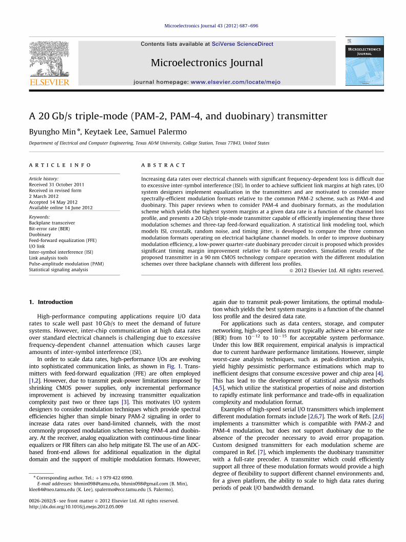
In order to scale data rates, high-performance I/Os are evolvinginto sophisticated communication links, as shown in Fig. 1. Trans-mitters with feed-forward equalization (FFE) are often employed[1,2]. However, due to transmit peak-power limitations imposed byshrinking CMOS power supplies, only incremental performanceimprovement is achieved by increasing transmitter equalizationcomplexity past two or three taps [3]. This motivates I/O systemdesigners to consider modulation techniques which provide spectralefficiencies higher than simple binary PAM-2 signaling in order toincrease data rates over band-limited channels, with the mostcommonly proposed modulation schemes being PAM-4 and duobin-ary. At the receiver, analog equalization with continuous-time linearequalizers or FIR filters can also help mitigate ISI. The use of an ADC-based front-end allows for additional equalization in the digitaldomain and the support of multiple modulation formats. However,
ll rights reserved.
[email protected] (B. Min),
du (S. Palermo).
again due to transmit peak-power limitations, the optimal modula-tion which yields the best system margins is a function of the channelloss profile and the desired data rate.
For applications such as data centers, storage, and computernetworking, high-speed links must typically achieve a bit-error rate(BER) from 10�12 to 10�15 for acceptable system performance.Under this low BER requirement, empirical analysis is impracticaldue to current hardware performance limitations. However, simpleworst-case analysis techniques, such as peak-distortion analysis,yield highly pessimistic performance estimations which map toinefficient designs that consume excessive power and chip area [4].This has lead to the development of statistical analysis methods[4,5], which utilize the statistical properties of noise and distortionto rapidly estimate link performance and trade-offs in equalizationcomplexity and modulation format.
Examples of high-speed serial I/O transmitters which implementdifferent modulation formats include [2,6,7]. The work of Refs. [2,6]implements a transmitter which is compatible with PAM-2 andPAM-4 modulation, but does not support duobinary due to theabsence of the precoder necessary to avoid error propagation.Custom designed transmitters for each modulation scheme arecompared in Ref. [7], which implements the duobinary transmitterwith a full-rate precoder. A transmitter which could efficientlysupport all three of these modulation formats would provide a highdegree of flexibility to support different channel environments and,for a given platform, the ability to scale to high data rates duringperiods of peak I/O bandwidth demand.
B. Min et al. / Microelectronics Journal 43 (2012) 687–696688
This paper presents a 20 Gb/s triple-mode transmitter capable ofefficiently implementing these three common modulation schemesand three-tap feed-forward equalization. Section 2 reviews thesupported modulation schemes and when to consider PAM-4 andduobinary as a function of the channel loss profile. A statistical linkmodeling tool is detailed in Section 3 and utilized to verify therelative performance and further discusses the trade-offs of thedifferent modulation formats and equalization complexity for threebackplane channels with differing loss profiles. Section 4 discussesthe design of the triple-mode transmitter, where a quarter-rateprecoder circuit allows for the efficient inclusion of duobinarymodulation. 90 nm CMOS simulation results of the triple-modetransmitter are presented in Section 5. Finally, Section 6 concludesthe paper.
2. Modulation techniques
2.1. Overview of PAM-2, PAM-4, and duobinary signaling
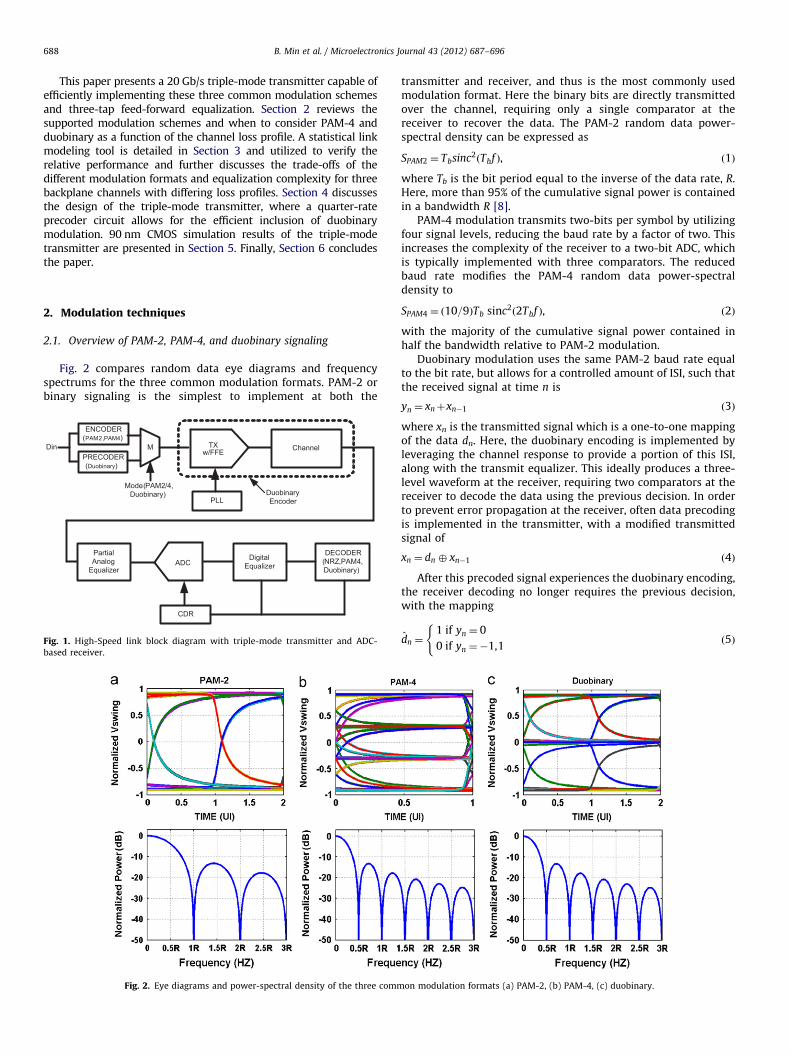
Fig. 2 compares random data eye diagrams and frequencyspectrums for the three common modulation formats. PAM-2 orbinary signaling is the simplest to implement at both the
Mode(PAM2/4, Duobinary)
Din
ENCODER
w/FFE
PLL
PartialAnalog
Equalizer
DigitalEqualizer
DECODER (NRZ,PAM4, Duobinary)
CDR
Channel
ADC
PRECODERM
Duobinary Encoder
TX
Fig. 1. High-Speed link block diagram with triple-mode transmitter and ADC-
based receiver.
Fig. 2. Eye diagrams and power-spectral density of the three comm
transmitter and receiver, and thus is the most commonly usedmodulation format. Here the binary bits are directly transmittedover the channel, requiring only a single comparator at thereceiver to recover the data. The PAM-2 random data power-spectral density can be expressed as
SPAM2 ¼ Tbsinc2ðTbf Þ, ð1Þ
where Tb is the bit period equal to the inverse of the data rate, R.Here, more than 95% of the cumulative signal power is containedin a bandwidth R [8].
PAM-4 modulation transmits two-bits per symbol by utilizingfour signal levels, reducing the baud rate by a factor of two. Thisincreases the complexity of the receiver to a two-bit ADC, whichis typically implemented with three comparators. The reducedbaud rate modifies the PAM-4 random data power-spectraldensity to
SPAM4 ¼ ð10=9ÞTb sinc2ð2Tbf Þ, ð2Þ
with the majority of the cumulative signal power contained inhalf the bandwidth relative to PAM-2 modulation.
Duobinary modulation uses the same PAM-2 baud rate equalto the bit rate, but allows for a controlled amount of ISI, such thatthe received signal at time n is
yn ¼ xnþxn�1 ð3Þ
where xn is the transmitted signal which is a one-to-one mappingof the data dn. Here, the duobinary encoding is implemented byleveraging the channel response to provide a portion of this ISI,along with the transmit equalizer. This ideally produces a three-level waveform at the receiver, requiring two comparators at thereceiver to decode the data using the previous decision. In orderto prevent error propagation at the receiver, often data precodingis implemented in the transmitter, with a modified transmittedsignal of
xn ¼ dn � xn�1 ð4Þ
After this precoded signal experiences the duobinary encoding,the receiver decoding no longer requires the previous decision,with the mapping
d̂n ¼1 if yn ¼ 0
0 if yn ¼�1,1
(ð5Þ
on modulation formats (a) PAM-2, (b) PAM-4, (c) duobinary.
B. Min et al. / Microelectronics Journal 43 (2012) 687–696 689
This controlled ISI results in a duobinary random data power-spectral density of
Sduo ¼ Tb sin c2ðTbf Þncos2ðpTbf Þ ¼ Tb sin c2ð2Tbf Þ, ð6Þ
which for a given data rate provides the same factor of twosignal bandwidth reduction as PAM-4 modulation.
2.2. Modulation selection
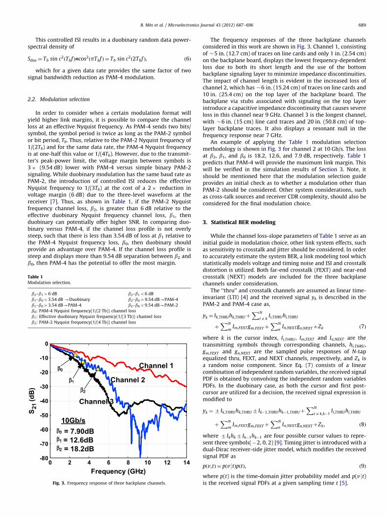
In order to consider when a certain modulation format willyield higher link margins, it is possible to compare the channelloss at an effective Nyquist frequency. As PAM-4 sends two bits/symbol, the symbol period is twice as long as the PAM-2 symbolor bit period, Tb. Thus, relative to the PAM-2 Nyquist frequency of1/(2Tb) and for the same data rate, the PAM-4 Nyquist frequencyis at one-half this value or 1/(4Tb). However, due to the transmit-ter’s peak-power limit, the voltage margin between symbols is3� (9.54 dB) lower with PAM-4 versus simple binary PAM-2signaling. While duobinary modulation has the same baud rate asPAM-2, the introduction of controlled ISI reduces the effectiveNyquist frequency to 1/(3Tb) at the cost of a 2� reduction involtage margin (6 dB) due to the three-level waveform at thereceiver [7]. Thus, as shown in Table 1, if the PAM-2 Nyquistfrequency channel loss, b2, is greater than 6 dB relative to theeffective duobinary Nyquist frequency channel loss, b1, thenduobinary can potentially offer higher SNR. In comparing duo-binary versus PAM-4, if the channel loss profile is not overlysteep, such that there is less than 3.54 dB of loss at b1 relative tothe PAM-4 Nyquist frequency loss, b0, then duobinary shouldprovide an advantage over PAM-4. If the channel loss profile issteep and displays more than 9.54 dB separation between b2 andb0, then PAM-4 has the potential to offer the most margin.
Table 1Modulation selection.
b2–b146 dB b2–b1o6 dB
b1–b0o3.54 dB -Duobinary b2–b049.54 dB-PAM-4
b1–b043.54 dB-PAM-4 b2–b0o9.54 dB-PAM-2
b0: PAM-4 Nyquist frequency(1/(2 Tb)) channel loss
b1: Effective duobinary Nyquist frequency(1/(3 Tb)) channel loss
b2: PAM-2 Nyquist frequency(1/(4 Tb)) channel loss
Fig. 3. Frequency response of three backplane channels.
The frequency responses of the three backplane channelsconsidered in this work are shown in Fig. 3. Channel 1, consistingof �5 in. (12.7 cm) of traces on line cards and only 1 in. (2.54 cm)on the backplane board, displays the lowest frequency-dependentloss due to both its short length and the use of the bottombackplane signaling layer to minimize impedance discontinuities.The impact of channel length is evident in the increased loss ofchannel 2, which has �6 in. (15.24 cm) of traces on line cards and10 in. (25.4 cm) on the top layer of the backplane board. Thebackplane via stubs associated with signaling on the top layerintroduce a capacitive impedance discontinuity that causes severeloss in this channel near 9 GHz. Channel 3 is the longest channel,with �6 in. (15 cm) line card traces and 20 in. (50.8 cm) of top-layer backplane traces. It also displays a resonant null in thefrequency response near 7 GHz.
An example of applying the Table 1 modulation selectionmethodology is shown in Fig. 3 for channel 2 at 10 Gb/s. The lossat b2, b1, and b0 is 18.2, 12.6, and 7.9 dB, respectively. Table 1predicts that PAM-4 will provide the maximum link margin. Thiswill be verified in the simulation results of Section 3. Note, itshould be mentioned here that the modulation selection guideprovides an initial check as to whether a modulation other thanPAM-2 should be considered. Other system considerations, suchas cross-talk sources and receiver CDR complexity, should also beconsidered for the final modulation choice.
3. Statistical BER modeling
While the channel loss-slope parameters of Table 1 serve as aninitial guide in modulation choice, other link system effects, suchas sensitivity to crosstalk and jitter should be considered. In orderto accurately estimate the system BER, a link modeling tool whichstatistically models voltage and timing noise and ISI and crosstalkdistortion is utilized. Both far-end crosstalk (FEXT) and near-endcrosstalk (NEXT) models are included for the three backplanechannels under consideration.
The ‘‘thru’’ and crosstalk channels are assumed as linear time-invariant (LTI) [4] and the received signal yk is described in thePAM-2 and PAM-4 case as,
yk ¼ Ik,THRUhk,THRUþXN
iakIi,THRUhi,THRU
þXN
mIm,FEXT gm,FEXTþ
XN
nIn,NEXT gn,NEXTþZk ð7Þ
where k is the cursor index, Ii,THRU , Im,FEXT and In,NEXT are thetransmitting symbols through corresponding channels, hi,THRU ,gm,FEXT and gn,NEXT are the sampled pulse responses of N-tapequalized thru, FEXT, and NEXT channels, respectively, and Zk isa random noise component. Since Eq. (7) consists of a linearcombination of independent random variables, the received signalPDF is obtained by convolving the independent random variablesPDFs. In the duobinary case, as both the cursor and first post-cursor are utilized for a decision, the received signal expression ismodified to
yk ¼ 7 Ik,THRUhk,THRU 7 Ik�1,THRUhk�1,THRUþXN
iak,k�1Ii,THRUhi,THRU
þXN
mIm,FEXT gm,FEXTþ
XN
nIn,NEXT gn,NEXTþZk, ð8Þ
where 7 Ikhk7 Ik�1hk�1 are four possible cursor values to repre-sent three symbols(�2, 0, 2) [9]. Timing jitter is introduced with adual-Dirac receiver-side jitter model, which modifies the receivedsignal PDF as
pðv,tÞ ¼ pðv9tÞpðtÞ, ð9Þ
where p(t) is the time-domain jitter probability model and p(v9t)is the received signal PDFs at a given sampling time t [5].
B. Min et al. / Microelectronics Journal 43 (2012) 687–696690
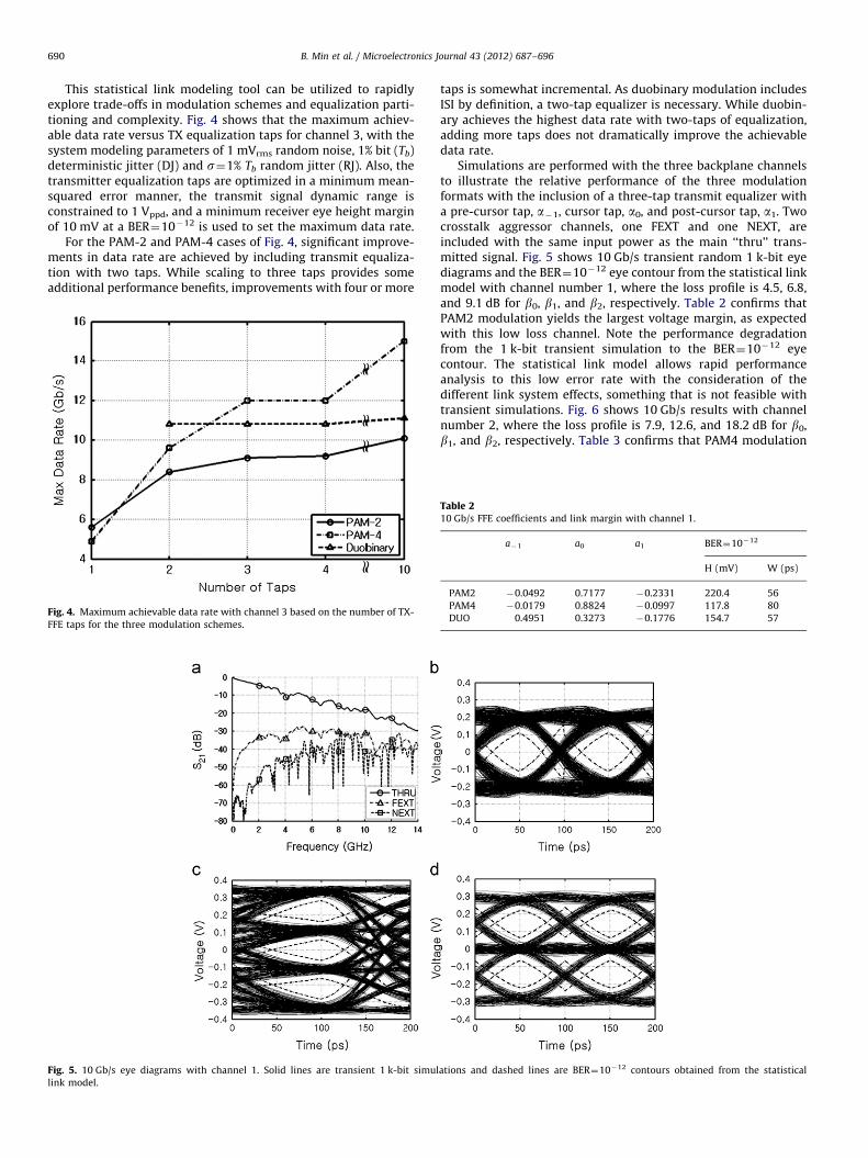
This statistical link modeling tool can be utilized to rapidlyexplore trade-offs in modulation schemes and equalization parti-tioning and complexity. Fig. 4 shows that the maximum achiev-able data rate versus TX equalization taps for channel 3, with thesystem modeling parameters of 1 mVrms random noise, 1% bit (Tb)deterministic jitter (DJ) and s¼1% Tb random jitter (RJ). Also, thetransmitter equalization taps are optimized in a minimum mean-squared error manner, the transmit signal dynamic range isconstrained to 1 Vppd, and a minimum receiver eye height marginof 10 mV at a BER¼10�12 is used to set the maximum data rate.
For the PAM-2 and PAM-4 cases of Fig. 4, significant improve-ments in data rate are achieved by including transmit equaliza-tion with two taps. While scaling to three taps provides someadditional performance benefits, improvements with four or more
Fig. 4. Maximum achievable data rate with channel 3 based on the number of TX-
FFE taps for the three modulation schemes.
Fig. 5. 10 Gb/s eye diagrams with channel 1. Solid lines are transient 1 k-bit simul
link model.
taps is somewhat incremental. As duobinary modulation includesISI by definition, a two-tap equalizer is necessary. While duobin-ary achieves the highest data rate with two-taps of equalization,adding more taps does not dramatically improve the achievabledata rate.
Simulations are performed with the three backplane channelsto illustrate the relative performance of the three modulationformats with the inclusion of a three-tap transmit equalizer witha pre-cursor tap, a�1, cursor tap, a0, and post-cursor tap, a1. Twocrosstalk aggressor channels, one FEXT and one NEXT, areincluded with the same input power as the main ‘‘thru’’ trans-mitted signal. Fig. 5 shows 10 Gb/s transient random 1 k-bit eyediagrams and the BER¼10�12 eye contour from the statistical linkmodel with channel number 1, where the loss profile is 4.5, 6.8,and 9.1 dB for b0, b1, and b2, respectively. Table 2 confirms thatPAM2 modulation yields the largest voltage margin, as expectedwith this low loss channel. Note the performance degradationfrom the 1 k-bit transient simulation to the BER¼10�12 eyecontour. The statistical link model allows rapid performanceanalysis to this low error rate with the consideration of thedifferent link system effects, something that is not feasible withtransient simulations. Fig. 6 shows 10 Gb/s results with channelnumber 2, where the loss profile is 7.9, 12.6, and 18.2 dB for b0,b1, and b2, respectively. Table 3 confirms that PAM4 modulation
ations and dashed lines are BER¼10�12 contours obtained from the statistical
Table 210 Gb/s FFE coefficients and link margin with channel 1.
a�1 a0 a1 BER¼10�12
H (mV) W (ps)
PAM2 �0.0492 0.7177 �0.2331 220.4 56
PAM4 �0.0179 0.8824 �0.0997 117.8 80
DUO 0.4951 0.3273 �0.1776 154.7 57
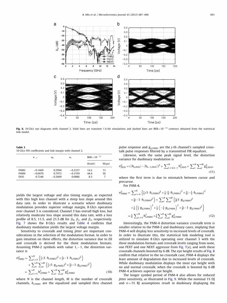
Fig. 6. 10 Gb/s eye diagrams with channel 2. Solid lines are transient 1 k-bit simulations and dashed lines are BER¼10�12 contours obtained from the statistical
link model.
Table 310 Gb/s FFE coefficients and link margin with channel 2.
a�1 a0 a1 BER¼10�12
H(mV) W(ps)
PAM2 �0.1669 0.5994 �0.2337 14.2 13
PAM4 �0.0470 0.7972 �0.1559 44.4 36
DUO 0.7246 �0.2669 0.0086 8.3 7
B. Min et al. / Microelectronics Journal 43 (2012) 687–696 691
yields the largest voltage and also timing margin, as expectedwith this high loss channel with a steep loss slope around thisdata rate. In order to illustrate a scenario where duobinarymodulation provides superior voltage margin, 8 Gb/s operationover channel 3 is considered. Channel 3 has overall high loss, butrelatively moderate loss slope around this data rate, with a lossprofile of 8.5, 11.5, and 21.5 dB for b0, b1, and b2, respectively.Fig. 7 shows the 8 Gb/s results and Table 4 confirms thatduobinary modulation yields the largest voltage margin.
Sensitivity to crosstalk and timing jitter are important con-siderations in the selection of the modulation format. In order togain intuition on these effects, the distortion variance due to ISIand crosstalk is derived for the three modulation formats.Assuming PAM-2 symbols with value 1,�1, the distortion var-iance is
s2PAM2 ¼
XN
iak12 ð1Uhi,PAM2Þ
2þ1
2ð�1Uhi,PAM2Þ2
n oþXN
i
XM
j12 ð1Ugij,PAM2Þ
2þ1
2ð�1Ugij,PAM2Þ2
n o¼XN
iakh2
i,PAM2þXN
i
XM
jg2
ij,PAM2 ð10Þ
where N is the channel length, M is the number of crosstalkchannels, hi,PAM2 are the equalized and sampled thru channel
pulse response and gij,PAM2 are the j-th channel’s sampled cross-talk pulse responses filtered by a transmitted FIR equalizer.
Likewise, with the same peak signal level, the distortionvariance for duobinary modulation is
s2DUO ¼ ð9hk,DUO9�9hk�1,DUO9Þ
2þXN
iak,k�1h2
i,DUOþXN
i
XM
jg2
ij,DUO,
ð11Þ
where the first term is due to mismatch between cursor andprecursor.
For PAM-4,
s2PAM4 ¼
XN
iak14 ð1Uhi,PAM4Þ
2þ1
413Uhi,PAM4
� �2þ1
4 �13Uhi,PAM4
� �2n
þ14ð�1Uhi,PAM4Þ
2oþXN
i
XM
j14ð1Ugij,PAM4Þ
2n
þ14
13Ugij,PAM4
� �2þ1
4 �13Ugij,PAM4
� �2þ1
4ð�1Ugij,PAM4Þ2
�
¼ 59
XN
iakh2
i,PAM4þ59
XN
i
XM
jg2
ij,PAM4 ð12Þ
Interestingly, the PAM-4 distortion variance crosstalk term issmaller relative to the PAM-2 and duobinary cases, implying thatPAM-4 will display less sensitivity to increased levels of crosstalk.In order to illustrate this, the statistical link modeling tool isutilized to simulate 8 Gb/s operating over channel 3 with thethree modulation formats and crosstalk levels ranging from none,one FEXT and one NEXT aggressor from Fig. 7(a), and with thesecrosstalk channels boosted by 6 dB. The eye height results of Fig. 8confirm that relative to the no crosstalk case, PAM-4 displays theleast amount of degradation due to increased levels of crosstalk.While duobinary modulation displays the most eye height withno and normal crosstalk, when the crosstalk is boosted by 6 dBPAM-4 achieves superior eye height.
The longer symbol period of PAM-4 also allows for reducedjitter sensitivity, as illustrated in Fig. 9. While the nominal 1% DJand s¼1% RJ assumptions result in duobinary displaying the
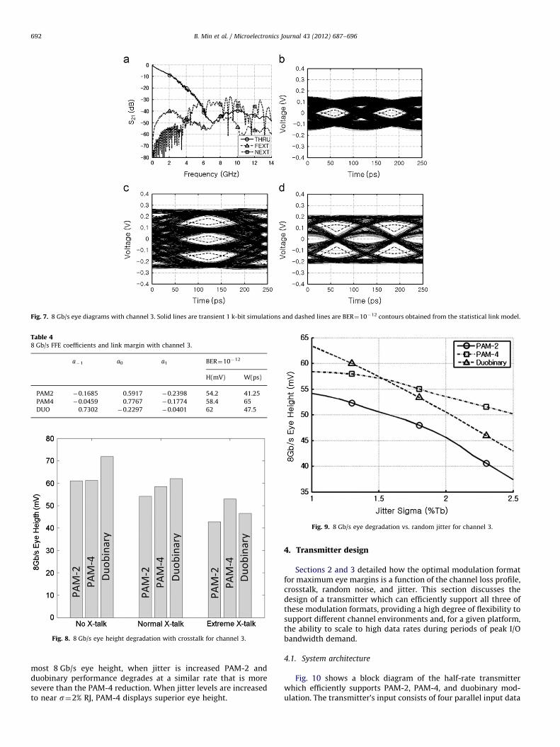
Fig. 7. 8 Gb/s eye diagrams with channel 3. Solid lines are transient 1 k-bit simulations and dashed lines are BER¼10�12 contours obtained from the statistical link model.
Table 48 Gb/s FFE coefficients and link margin with channel 3.
a�1 a0 a1 BER¼10�12
H(mV) W(ps)
PAM2 �0.1685 0.5917 �0.2398 54.2 41.25
PAM4 �0.0459 0.7767 �0.1774 58.4 65
DUO 0.7302 �0.2297 �0.0401 62 47.5
Fig. 8. 8 Gb/s eye height degradation with crosstalk for channel 3.
Fig. 9. 8 Gb/s eye degradation vs. random jitter for channel 3.
B. Min et al. / Microelectronics Journal 43 (2012) 687–696692
most 8 Gb/s eye height, when jitter is increased PAM-2 andduobinary performance degrades at a similar rate that is moresevere than the PAM-4 reduction. When jitter levels are increasedto near s¼2% RJ, PAM-4 displays superior eye height.
4. Transmitter design
Sections 2 and 3 detailed how the optimal modulation formatfor maximum eye margins is a function of the channel loss profile,crosstalk, random noise, and jitter. This section discusses thedesign of a transmitter which can efficiently support all three ofthese modulation formats, providing a high degree of flexibility tosupport different channel environments and, for a given platform,the ability to scale to high data rates during periods of peak I/Obandwidth demand.
4.1. System architecture
Fig. 10 shows a block diagram of the half-rate transmitterwhich efficiently supports PAM-2, PAM-4, and duobinary mod-ulation. The transmitter’s input consists of four parallel input data
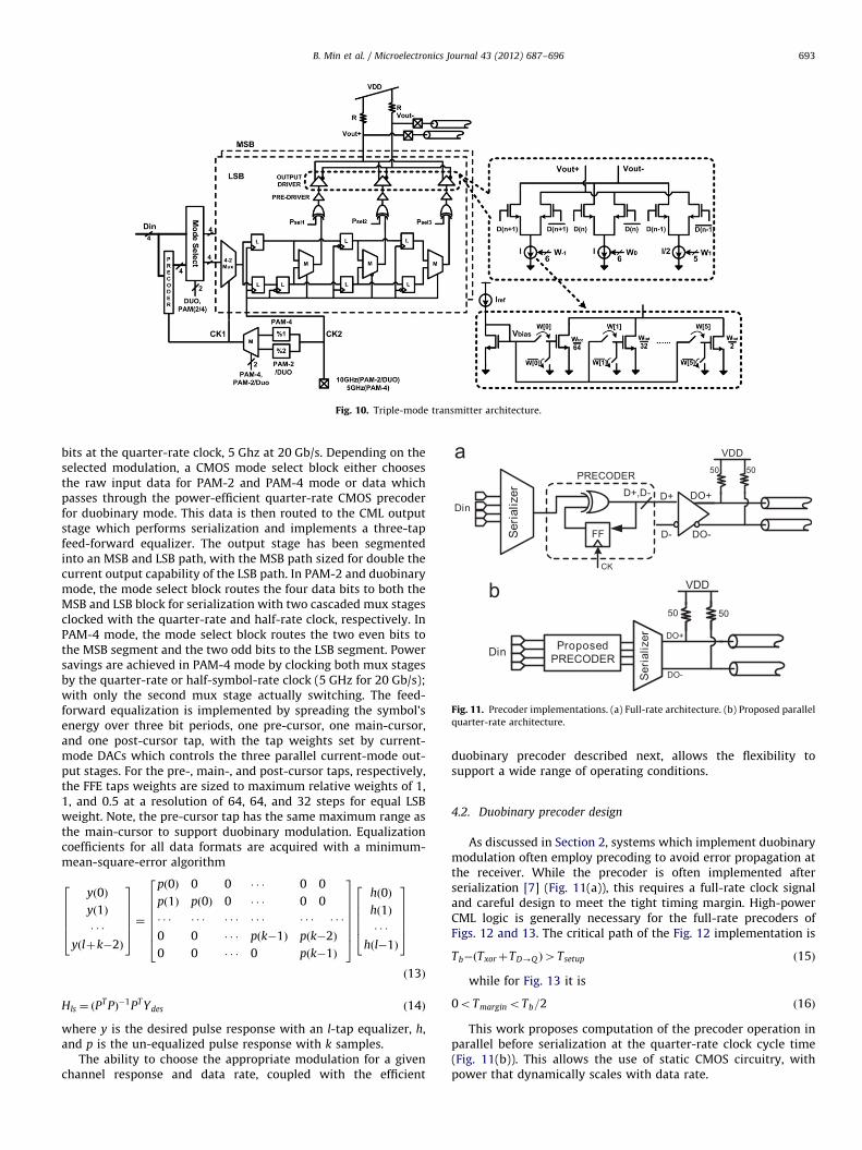
Fig. 10. Triple-mode transmitter architecture.
Seria
lizer
PRECODER
DO-
DO+
VDD5050
Din
FF
CK
D+,D- D+
D-
ProposedPRECODER
DO+
DO-
50 50
VDD
DinSe
rializ
er
Fig. 11. Precoder implementations. (a) Full-rate architecture. (b) Proposed parallel
quarter-rate architecture.
B. Min et al. / Microelectronics Journal 43 (2012) 687–696 693
bits at the quarter-rate clock, 5 Ghz at 20 Gb/s. Depending on theselected modulation, a CMOS mode select block either choosesthe raw input data for PAM-2 and PAM-4 mode or data whichpasses through the power-efficient quarter-rate CMOS precoderfor duobinary mode. This data is then routed to the CML outputstage which performs serialization and implements a three-tapfeed-forward equalizer. The output stage has been segmentedinto an MSB and LSB path, with the MSB path sized for double thecurrent output capability of the LSB path. In PAM-2 and duobinarymode, the mode select block routes the four data bits to both theMSB and LSB block for serialization with two cascaded mux stagesclocked with the quarter-rate and half-rate clock, respectively. InPAM-4 mode, the mode select block routes the two even bits tothe MSB segment and the two odd bits to the LSB segment. Powersavings are achieved in PAM-4 mode by clocking both mux stagesby the quarter-rate or half-symbol-rate clock (5 GHz for 20 Gb/s);with only the second mux stage actually switching. The feed-forward equalization is implemented by spreading the symbol’senergy over three bit periods, one pre-cursor, one main-cursor,and one post-cursor tap, with the tap weights set by current-mode DACs which controls the three parallel current-mode out-put stages. For the pre-, main-, and post-cursor taps, respectively,the FFE taps weights are sized to maximum relative weights of 1,1, and 0.5 at a resolution of 64, 64, and 32 steps for equal LSBweight. Note, the pre-cursor tap has the same maximum range asthe main-cursor to support duobinary modulation. Equalizationcoefficients for all data formats are acquired with a minimum-mean-square-error algorithm
yð0Þ
yð1Þ
� � �
yðlþk�2Þ
266664
377775¼
pð0Þ 0 0 � � � 0 0
pð1Þ pð0Þ 0 � � � 0 0
� � � � � � � � � � � � � � � � � �
0 0 � � � pðk�1Þ pðk�2Þ
0 0 � � � 0 pðk�1Þ
26666664
37777775
hð0Þ
hð1Þ
� � �
hðl�1Þ
266664
377775ð13Þ
Hls ¼ ðPT PÞ�1PT Ydes ð14Þ
where y is the desired pulse response with an l-tap equalizer, h,and p is the un-equalized pulse response with k samples.
The ability to choose the appropriate modulation for a givenchannel response and data rate, coupled with the efficient
duobinary precoder described next, allows the flexibility tosupport a wide range of operating conditions.
4.2. Duobinary precoder design
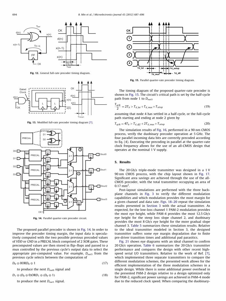
As discussed in Section 2, systems which implement duobinarymodulation often employ precoding to avoid error propagation atthe receiver. While the precoder is often implemented afterserialization [7] (Fig. 11(a)), this requires a full-rate clock signaland careful design to meet the tight timing margin. High-powerCML logic is generally necessary for the full-rate precoders ofFigs. 12 and 13. The critical path of the Fig. 12 implementation is
Tb�ðTxorþTD-Q Þ4Tsetup ð15Þ
while for Fig. 13 it is
0oTmarginoTb=2 ð16Þ
This work proposes computation of the precoder operation inparallel before serialization at the quarter-rate clock cycle time(Fig. 11(b)). This allows the use of static CMOS circuitry, withpower that dynamically scales with data rate.
FF
d(n)x(n)
x(n-1)
CK
Txor
TD Q
CK
d(n)
x(n-1)
x(n)
TxorTD Q
Fig. 12. General full-rate precoder timing diagram.
L L
CK
GatedClock
CK
d(n)
x(n)x(n)
x(n)
d(n)
Fig. 13. Modified full-rate precoder timing diagram [7].
PRECALgnd D
vdd
vdd
gnd
D0
D1
D2
D3
D
D
D
D
D
D
D
L
2:1
2:1
2:1
2:1 D
D
D
D
gnd/vdd
D1
D2
PRECAL
PRECAL
PRECAL
CK1
Dout0
Dout1
Dout2
Dout3
L
L
L
PRECAL
12
3
4
Fig. 14. Parallel quarter-rate precoder circuit.
Fig. 15. Parallel quarter-rate precoder timing diagram.
B. Min et al. / Microelectronics Journal 43 (2012) 687–696694
The proposed parallel precoder is shown in Fig. 14. In order toimprove the precoder timing margin, the input data is specula-tively computed with the two possible previous precoded valuesof VDD or GND in a PRECAL block comprised of 2 XOR gates. Theseprecomputed values are then stored in flip–flops and passed to amux controlled by the previous cycle’s output data to select theappropriate pre-computed value. For example, Dout3 from theprevious cycle selects between the computation of
D0 � 0ORD0 � 1 ð17Þ
to produce the next Dout0 signal and
D1 � ðD0 � 0ÞORD1 � ðD0 � 1Þ ð18Þ
to produce the next Dout1 signal.
The timing diagram of the proposed quarter-rate precoder isshown in Fig. 15. The circuit’s critical path is set by the half-cyclepath from node 1 to Dout3
Tqclk
2¼ 2Tb4Td_latþTd_muxþTsetup ð19Þ
assuming that node 4 has settled in a half-cycle, or the full-cyclepath starting and ending at node 2 given by
Tqclk ¼ 4Tb4Td_df f þ2Td_muxþTsetup ð20Þ
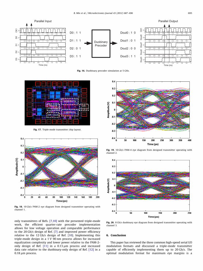
The simulation results of Fig. 16, performed in a 90 nm CMOSprocess, verify the duobinary precoder operation at 5 GHz. Thefour parallel incoming data bits are correctly precoded accordingto Eq. (4). Executing the precoding in parallel at the quarter-rateclock frequency allows for the use of an all-CMOS design thatoperates at the nominal 1 V supply.
5. Results
The 20 Gb/s triple-mode transmitter was designed in a 1 V90 nm CMOS process, with the chip layout shown in Fig. 17.Significant area savings are achieved through the use of the all-CMOS precoder, with the total transmitter occupying an area of0.17 mm2.
Post-layout simulations are performed with the three back-plane channels in Fig. 3 to verify the different modulationcapabilities and which modulation provides the most margin fora given channel and data rate. Figs. 18–20 repeat the simulationresults presented in Section 3 with the actual transmitter. Asexpected, for the low-loss channel 1 PAM-2 modulation providesthe most eye height, while PAM-4 provides the most 12.5 Gb/seye height for the steep loss slope channel 2, and duobinaryprovides the most 8 Gb/s eye height for the more gradual slopechannel 3. Table 5 summarizes these simulation results. Relativeto the ideal transmitter modeled in Section 3, the designedtransmitter suffers some eye margin degradation due to finitepre-driver transition times and additional pad parasitics.
Fig. 21 shows eye diagrams with an ideal channel to confirm20 Gb/s operation. Table 6 summarizes the 20 Gb/s transmitterperformance and compares the design with other recent high-speed serial I/O transmitters. Relative to the work of Ref. [7],which implemented three separate transmitters to compare thedifferent modulation schemes, the presented work allows for theefficient implementation of the three modulation schemes in asingle design. While there is some additional power overhead inthe presented PAM-2 design relative to a design optimized onlyfor PAM-2, significant power savings are achieved in PAM-4 modedue to the reduced clock speed. When comparing the duobinary-
CK
1D
out0
Dou
t1D
out2
Dou
t3
Time (ns)
CK
1D
0D
1D
2D
3
Time (ns)
DuobinaryPrecoder
D
Parallel Input Parallel Output
0 : 1 1
D1 : 1 1
D2 : 0 1
D3 : 1 1
Dout0 : 1 0
Dout1 : 0 1
Dout2 : 0 0
Dout3 : 1 1
Fig. 16. Duobinary precoder simulation at 5 GHz.
Fig. 17. Triple-mode transmitter chip layout.
Fig. 18. 10 Gb/s PAM-2 eye diagram from designed transmitter operating with
channel 1.
Fig. 19. 10 Gb/s PAM-4 eye diagram from designed transmitter operating with
channel 2.
Fig. 20. 8 Gb/s duobinary eye diagram from designed transmitter operating with
channel 3.
B. Min et al. / Microelectronics Journal 43 (2012) 687–696 695
only transmitters of Refs. [7,10] with the presented triple-modework, the efficient quarter-rate precoder implementationallows for low voltage operation and comparable performanceto the 20 Gb/s design of Ref. [7] and improved power efficiencyrelative to the 12 Gb/s design of Ref. [10]. Implementing thistriple-mode design in a 1 V 90 nm process allows for increasedequalization complexity and lower power relative to the PAM-2-only design of Ref. [11] in a 0.13 mm process and increaseddata rate relative to the duobinary-only design of Ref. [12] in a0.18 mm process.
6. Conclusion
This paper has reviewed the three common high-speed serial I/Omodulation formats and discussed a triple-mode transmittercapable of efficiently implementing them up to 20 Gb/s. Theoptimal modulation format for maximum eye margins is a
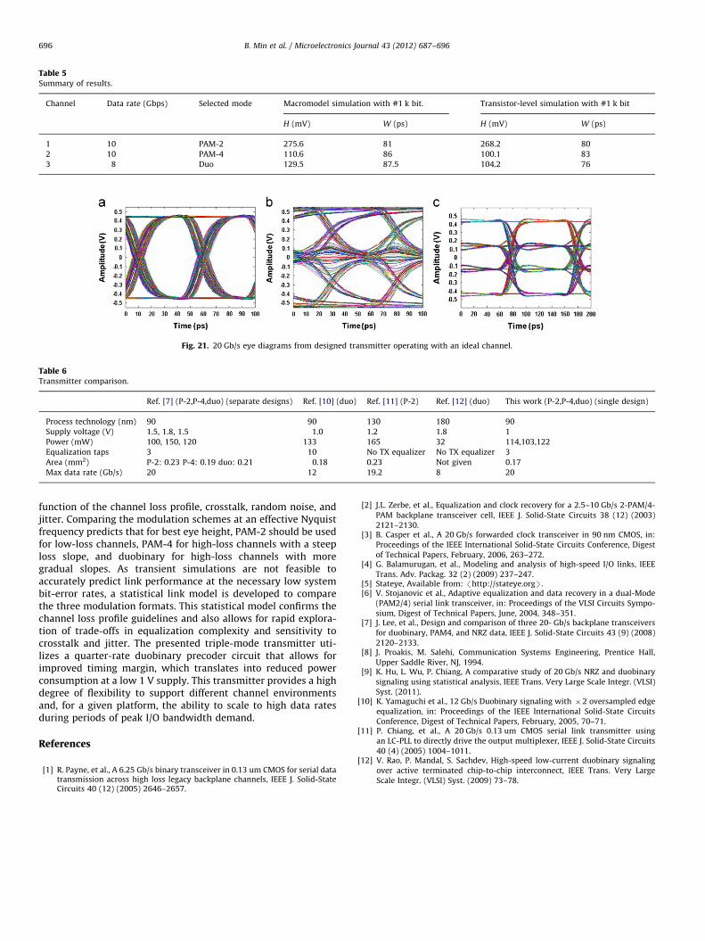
Table 5Summary of results.
Channel Data rate (Gbps) Selected mode Macromodel simulation with #1 k bit. Transistor-level simulation with #1 k bit
H (mV) W (ps) H (mV) W (ps)
1 10 PAM-2 275.6 81 268.2 80
2 10 PAM-4 110.6 86 100.1 83
3 8 Duo 129.5 87.5 104.2 76
Fig. 21. 20 Gb/s eye diagrams from designed transmitter operating with an ideal channel.
Table 6Transmitter comparison.
Ref. [7] (P-2,P-4,duo) (separate designs) Ref. [10] (duo) Ref. [11] (P-2) Ref. [12] (duo) This work (P-2,P-4,duo) (single design)
Process technology (nm) 90 90 130 180 90
Supply voltage (V) 1.5, 1.8, 1.5 1.0 1.2 1.8 1
Power (mW) 100, 150, 120 133 165 32 114,103,122
Equalization taps 3 10 No TX equalizer No TX equalizer 3
Area (mm2) P-2: 0.23 P-4: 0.19 duo: 0.21 0.18 0.23 Not given 0.17
Max data rate (Gb/s) 20 12 19.2 8 20
B. Min et al. / Microelectronics Journal 43 (2012) 687–696696
function of the channel loss profile, crosstalk, random noise, andjitter. Comparing the modulation schemes at an effective Nyquistfrequency predicts that for best eye height, PAM-2 should be usedfor low-loss channels, PAM-4 for high-loss channels with a steeploss slope, and duobinary for high-loss channels with moregradual slopes. As transient simulations are not feasible toaccurately predict link performance at the necessary low systembit-error rates, a statistical link model is developed to comparethe three modulation formats. This statistical model confirms thechannel loss profile guidelines and also allows for rapid explora-tion of trade-offs in equalization complexity and sensitivity tocrosstalk and jitter. The presented triple-mode transmitter uti-lizes a quarter-rate duobinary precoder circuit that allows forimproved timing margin, which translates into reduced powerconsumption at a low 1 V supply. This transmitter provides a highdegree of flexibility to support different channel environmentsand, for a given platform, the ability to scale to high data ratesduring periods of peak I/O bandwidth demand.
References
[1] R. Payne, et al., A 6.25 Gb/s binary transceiver in 0.13 um CMOS for serial datatransmission across high loss legacy backplane channels, IEEE J. Solid-StateCircuits 40 (12) (2005) 2646–2657.
[2] J.L. Zerbe, et al., Equalization and clock recovery for a 2.5–10 Gb/s 2-PAM/4-
PAM backplane transceiver cell, IEEE J. Solid-State Circuits 38 (12) (2003)2121–2130.
[3] B. Casper et al., A 20 Gb/s forwarded clock transceiver in 90 nm CMOS, in:Proceedings of the IEEE International Solid-State Circuits Conference, Digest
of Technical Papers, February, 2006, 263–272.[4] G. Balamurugan, et al., Modeling and analysis of high-speed I/O links, IEEE
Trans. Adv. Packag. 32 (2) (2009) 237–247.[5] Stateye, Available from: /http://stateye.orgS.[6] V. Stojanovic et al., Adaptive equalization and data recovery in a dual-Mode
(PAM2/4) serial link transceiver, in: Proceedings of the VLSI Circuits Sympo-sium, Digest of Technical Papers, June, 2004, 348–351.
[7] J. Lee, et al., Design and comparison of three 20- Gb/s backplane transceiversfor duobinary, PAM4, and NRZ data, IEEE J. Solid-State Circuits 43 (9) (2008)
2120–2133.[8] J. Proakis, M. Salehi, Communication Systems Engineering, Prentice Hall,
Upper Saddle River, NJ, 1994.[9] K. Hu, L. Wu, P. Chiang, A comparative study of 20 Gb/s NRZ and duobinary
signaling using statistical analysis, IEEE Trans. Very Large Scale Integr. (VLSI)Syst. (2011).
[10] K. Yamaguchi et al., 12 Gb/s Duobinary signaling with �2 oversampled edgeequalization, in: Proceedings of the IEEE International Solid-State CircuitsConference, Digest of Technical Papers, February, 2005, 70–71.
[11] P. Chiang, et al., A 20 Gb/s 0.13 um CMOS serial link transmitter usingan LC-PLL to directly drive the output multiplexer, IEEE J. Solid-State Circuits
40 (4) (2005) 1004–1011.[12] V. Rao, P. Mandal, S. Sachdev, High-speed low-current duobinary signaling
over active terminated chip-to-chip interconnect, IEEE Trans. Very LargeScale Integr. (VLSI) Syst. (2009) 73–78.