Embed Size (px)
Citation preview

A 18mW, 3.3dB NF, 60GHz LNA in 32nm SOI CMOS
Technology with Autonomic NF Calibration
J.-O. Plouchart1, F. Wang2, A. Balteanu1, B. Parker1, M. A. T. Sanduleanu1, M. Yeck1,
Chen1, W. Woods3, B. Sadhu1, A. Valdes-Garcia1, X. Li2, and D. Friedman1
1IBM T. J. Watson Research Center, Yorktown Heights, NY, USA 2Electrical & Computer Engineering Department, Carnegie Mellon University, Pittsburgh, PA, USA
3IBM Semiconductor Research and Development Center, Essex Junction, VT
Abstract— A self-healing mmWave SoC integrating an 8052
microcontroller with 12kB of memory, an ADC, a temperature
sensor, and a 3-stage cascode 60GHz LNA, implemented in a
32nm SOI CMOS technology exhibits a peak gain of 21dB, an
average 3.3dB NF from 53 to 62GHz and 18mW power
consumption. An indirect NF sensing algorithm was
implemented on the integrated uC, which enables an adaptive
biasing algorithm to reduce the 60GHz NF sigma and LNA
power consumption by 37 and 40%, respectively, across P,V,T.
Index Terms—Mm-wave, SoC, NF, LNA, 60GHz,
autonomic calibration.
I. INTRODUCTION
The design of millimeter-wave (mmWave) transceivers
in advanced CMOS technology nodes are attractive due to
high fT, fMAX and its integration with complex digital
circuits. However such a design remains a challenge due to
device modelling uncertainties and sensitivities to process
(P), supply voltage (V), and temperature (T) variations.
This challenge has motivated research in the area of self-
healing circuit capabilities for mmWave circuits [1]-[2].
Note, however, that mmWave transceiver (TRx)
measurements are difficult even using external
measurement equipment, and further that integrating on-
chip direct mmWave measurement infrastructure is in most
cases not feasible. A potential solution to this problem
presented in [3] is to perform indirect performance sensing
by using a set of easily measurable metrics (e.g., DC bias
current) to predict performance metrics of interest that are
difficult to measure directly using on-chip sensors. An
indirect VCO phase noise performance sensing method was
demonstrated in [4], here to adaptively tune a VCO to
improve its performance and/or yield. A 1.5GHz and
2.4GHz LNAs with linearity and gain [5] and S11/S21
healing capabilities [6] were also reported. For mmWave
LNA noise figure (NF), a self-healing approach was
presented and evaluated through simulations in [7]. In this
work, we present the hardware implementation and
measurements results for a self-healing 60GHz LNA.
II. MMWAVE SOC LNA DESIGN
Fig. 1 shows the SoC LNA block diagram and the
detailed cascode amplifier stage schematic. The overall
design was implemented in a 32nm SOI process. The
implementation of on-chip healing algorithms requires
complex SoC design, especially for a mmwave TRx. In this
architecture, the serial interface and microcontroller data
flows are multiplexed such that the algorithm can be run
either outside of the chip on a host or inside the chip on the
microcontroller.
Fig. 1. Circuit block and cascode amplifier stage schematic.
A microcontroller was chosen for the healing
implementation because it offers the flexibility to enhance
the algorithm once the chip is tested or in the field,
providing additional configurability as compared to a
dedicated/fixed algorithm implementation in hardware. The
healing architecture is scalable to a large number of circuits,
or a full TRx, as well as an array of TRx. Since the uC, the
T sensor, and the ADCs would be shared by all the circuits,
the ratio between the circuit area dedicated to self-healing
and the TRx area decreases as the TRx gets more complex.
The uC with its 12kB of memory occupies only 0.25x1mm2,
V. H.-C.
978-1-4799-7642-3/15/$31.00 © 2015 IEEE 2015 IEEE Radio Frequency Integrated Circuits Symposium
RTU2B-1
319
which is a significant fraction of the LNA area, but a small
fraction of the area required for a full mmWave TRx. Note
that one limitation of this approach is that since the uC
clock frequency is in the MHz range, the self-healing loop
latency will inevitably be in the usec range, which is
sufficient for most of the self-healing applications but not
for applications demanding ultra-fast feedback.
The LNA itself consists of an input matching networks
and three identical cascode amplifier stages. Each
individual cascode amplifier stage integrates two actuators.
The first of these is the DAC actuator which allows bias
current adjustment. The second actuator is the digital
control that enables the inductance and capacitance of the
transmission line used in the cascode amplifier load to be
varied [8]. The digitally tuneable line is used to tune the
frequency response of the amplifier. The sensor is the ADC
used to convert the voltage Vsens1, which tracks the DC
voltage between the drain of the input stage and the source
of the output stage. The FETs, along with all the wire
parasitics, were extracted from the layout to enable accurate
simulation. The circuit was simulated using high frequency
models for the transmission lines, capacitors, and resistors
used in the design.
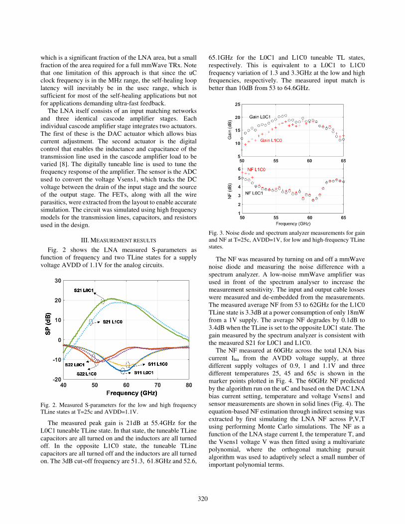
III. MEASUREMENT RESULTS
Fig. 2 shows the LNA measured S-parameters as
function of frequency and two TLine states for a supply
voltage AVDD of 1.1V for the analog circuits.
Fig. 2. Measured S-parameters for the low and high frequency
TLine states at T=25c and AVDD=1.1V.
The measured peak gain is 21dB at 55.4GHz for the
L0C1 tuneable TLine state. In that state, the tuneable TLine
capacitors are all turned on and the inductors are all turned
off. In the opposite L1C0 state, the tuneable TLine
capacitors are all turned off and the inductors are all turned
on. The 3dB cut-off frequency are 51.3, 61.8GHz and 52.6,
65.1GHz for the L0C1 and L1C0 tuneable TL states,
respectively. This is equivalent to a L0C1 to L1C0
frequency variation of 1.3 and 3.3GHz at the low and high
frequencies, respectively. The measured input match is
better than 10dB from 53 to 64.6GHz.
Fig. 3. Noise diode and spectrum analyzer measurements for gain
and NF at T=25c, AVDD=1V, for low and high-frequency TLine
states.
The NF was measured by turning on and off a mmWave
noise diode and measuring the noise difference with a
spectrum analyzer. A low-noise mmWave amplifier was
used in front of the spectrum analyser to increase the
measurement sensitivity. The input and output cable losses
were measured and de-embedded from the measurements.
The measured average NF from 53 to 62GHz for the L1C0
TLine state is 3.3dB at a power consumption of only 18mW
from a 1V supply. The average NF degrades by 0.1dB to
3.4dB when the TLine is set to the opposite L0C1 state. The
gain measured by the spectrum analyzer is consistent with
the measured S21 for L0C1 and L1C0.
The NF measured at 60GHz across the total LNA bias
current Ilna from the AVDD voltage supply, at three
different supply voltages of 0.9, 1 and 1.1V and three
different temperatures 25, 45 and 65c is shown in the
marker points plotted in Fig. 4. The 60GHz NF predicted
by the algorithm run on the uC and based on the DAC LNA
bias current setting, temperature and voltage Vsens1 and
sensor measurements are shown in solid lines (Fig. 4). The
equation-based NF estimation through indirect sensing was
extracted by first simulating the LNA NF across P,V,T
using performing Monte Carlo simulations. The NF as a
function of the LNA stage current I, the temperature T, and
the Vsens1 voltage V was then fitted using a multivariate
polynomial, where the orthogonal matching pursuit
algorithm was used to adaptively select a small number of
important polynomial terms.
320
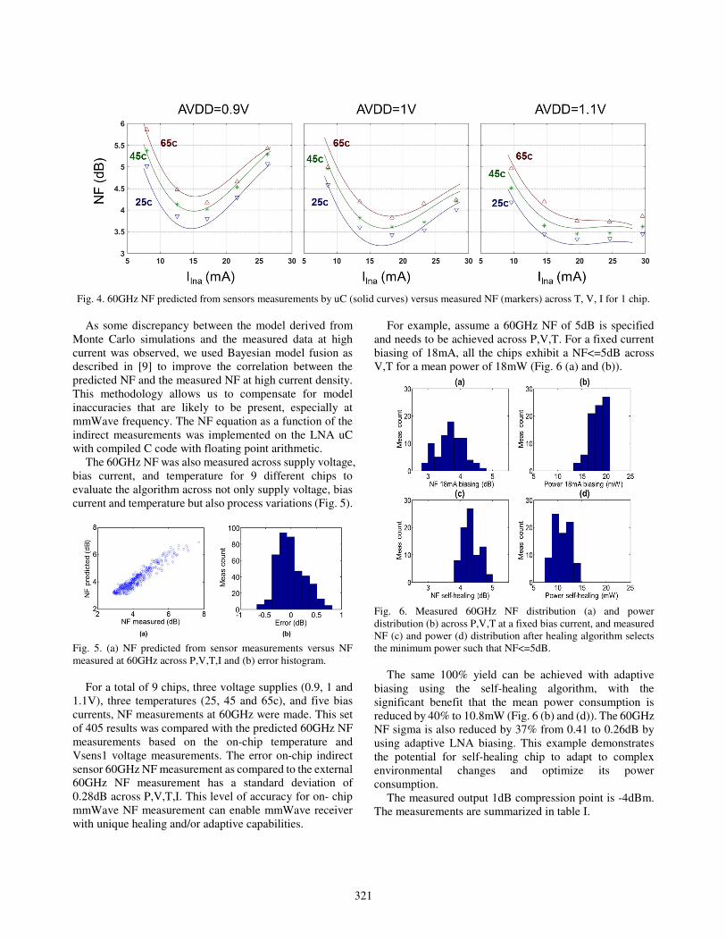
Fig. 4. 60GHz NF predicted from sensors measurements by uC (solid curves) versus measured NF (markers) across T, V, I for 1 chip.
As some discrepancy between the model derived from
Monte Carlo simulations and the measured data at high
current was observed, we used Bayesian model fusion as
described in [9] to improve the correlation between the
predicted NF and the measured NF at high current density.
This methodology allows us to compensate for model
inaccuracies that are likely to be present, especially at
mmWave frequency. The NF equation as a function of the
indirect measurements was implemented on the LNA uC
with compiled C code with floating point arithmetic.
The 60GHz NF was also measured across supply voltage,
bias current, and temperature for 9 different chips to
evaluate the algorithm across not only supply voltage, bias
current and temperature but also process variations (Fig. 5).
Fig. 5. (a) NF predicted from sensor measurements versus NF
measured at 60GHz across P,V,T,I and (b) error histogram.
For a total of 9 chips, three voltage supplies (0.9, 1 and
1.1V), three temperatures (25, 45 and 65c), and five bias
currents, NF measurements at 60GHz were made. This set
of 405 results was compared with the predicted 60GHz NF
measurements based on the on-chip temperature and
Vsens1 voltage measurements. The error on-chip indirect
sensor 60GHz NF measurement as compared to the external
60GHz NF measurement has a standard deviation of
0.28dB across P,V,T,I. This level of accuracy for on- chip
mmWave NF measurement can enable mmWave receiver
with unique healing and/or adaptive capabilities.
For example, assume a 60GHz NF of 5dB is specified
and needs to be achieved across P,V,T. For a fixed current
biasing of 18mA, all the chips exhibit a NF<=5dB across
V,T for a mean power of 18mW (Fig. 6 (a) and (b)).
Fig. 6. Measured 60GHz NF distribution (a) and power
distribution (b) across P,V,T at a fixed bias current, and measured
NF (c) and power (d) distribution after healing algorithm selects
the minimum power such that NF<=5dB.
The same 100% yield can be achieved with adaptive
biasing using the self-healing algorithm, with the
significant benefit that the mean power consumption is
reduced by 40% to 10.8mW (Fig. 6 (b) and (d)). The 60GHz
NF sigma is also reduced by 37% from 0.41 to 0.26dB by
using adaptive LNA biasing. This example demonstrates
the potential for self-healing chip to adapt to complex
environmental changes and optimize its power
consumption.
The measured output 1dB compression point is -4dBm.
The measurements are summarized in table I.
321
Fig. 7 shows the mmWave LNA SoC including the uC,
SRAM, serial interface, bandgap, PTAT, T sensor and SAR
ADC. The chip area is 1.94mm by 1.12mm.
Fig. 7. Chip micrograph.
TABLE I: MEASUREMENT RESULT SUMMARY
To the best of the author’s knowledge, the lowest
reported NF for 60GHz Si-based LNAs are between 4 and
5.5dB [10]-[13], which are higher than the measured
average 60GHz NF of 3.3dB for this 32nm SOI LNA.
IV. CONCLUSION
A self-healing 60GHz LNA was demonstrated in a 32nm
SOI CMOS technology. The measured peak LNA gain is
21dB at 55.4GHz, and an average 3.3dB NF from 53 to
62GHz is measured for a power consumption of only
18mW on a 1V supply. The healing algorithm was
implemented on the integrated uC. Good agreement
between the self-healing NF predicted from DC
measurements and the external 60GHz NF measurements
was achieved over a broad LNA bias current voltage supply
and temperature range. This demonstrates that difficult
mmwave measurements such as NF can be performed
indirectly and integrated efficiently on-chip. These results
are an important step towards self-adaptive TRx circuits
and systems that can minimize energy needed to transmit
and receive under varying environmental conditions.
ACKNOWLEDGMENT
The authors thank Roger Moussalli for support with uC
evaluation. This work is sponsored by the DARPA
HEALICS program under Air Force Research Laboratory
(AFRL) contract FA8650-09-C-7924. The views expressed
are those of the author and do not reflect the official policy
or position of the Department of Defense or the U.S.
Government.
REFERENCES
[1] C. Maxey, G. Creech, S. Raman, and J. Rockway, “Mixed-
signal SoCs with in situ self-healing circuitry,” IEEE Design
& Test of Computers, vol. 29, no. 6, pp. 27-39, Dec. 2012.
[2] C. Chien et al., “Dual-control self-healing architecture for
high-performance radio SoCs,” IEEE Design & Test of
Computers, vol. 29, no. 6, pp. 40-51, Dec. 2012.
[3] S. Sun et al., “Indirect Performance Sensing for On-Chip
Self-Healing of Analog and RF Circuits,” IEEE
Transactions on Circuits and Systems, vol. 61, no. 8, pp.
2243-2252, Aug. 2014.
[4] B. Sadhu et al., “A linearized, low-phase-noise VCO-based
25-GHz PLL with autonomic biasing,” IEEE Journal of
Solid-State Circuits, vol. 48, no. 5, pp. 1138-1150, May
2013.
[5] S. Sen et al, “A power-scalable channel-adaptive wireless
receiver based on built-In orthogonally tunable LNA,” IEEE
Transactions on Circuits and Systems, vol. 59, no. 5, pp.
946-957, May 2012.
[6] K. Jayaraman et al. “A self-healing 2.4GHz LNA with on-
chip S11/S21 measurement/calibration for in-situ PVT
compensation,” IEEE RFIC Symposium, Jun. 2010, pp. 311-
314.
[7] J.-O. Plouchart et al., “Adaptive Circuit Design
Methodology and Test Applied to Millimeter-wave Circuits,”
IEEE Design & Test, issue 99, 2014.
[8] W. H. Woods et al., “CMOS Millimeter Wave Phase Shifter
Based on Tunable Transmission Lines,” IEEE Custom
Integrated Circuits Conference, pp. 1-4, Sep. 2013.
[9] F. Wang et al, “Bayesian model fusion: large-scale
performance modeling of analog and mixed-signal circuits
by reusing early-stage data,” in Proceedings of Design
Automation Conference, pp. 1-6, Jun. 2013
[10] H-H Hsieh et al., “60GHz High-Gain Low-Noise Amplifiers
with a Common-Gate Inductive Feedback in 65nm CMOS,”
IEEE RFIC Symposium, Jun. 2011, pp. 1-4.
[11] T. Yao et al., Algorithmic Design of CMOS LNAs and PAs
for 60-GHz Radio,” IEEE Journal of Solid-State Circuits,
vol. 42, no. 5, pp. 1044-1057, May 2007.
[12] B. A. Floyd et al., “SiGe bipolar transceiver circuits
operating at 60 GHz,” IEEE Journal of Solid-State Circuits,
vol. 40, no. 1, pp. 156–157, Jan. 2005.
[13] M. Uzunkol and G. M. Rebeiz “A 65 GHz LNA/Phase
Shifter With 4.3 dB NF Using 45 nm CMOS SOI,” IEEE
Microwave and Wireless Components Letters, vol. 22, no.
10, pp. 530-532, Oct. 2012.
322


![g]kfnL nf sjftf] tyf nf{ ]shLjg](https://img.pdfslide.us/doc/110x75/62091bd4c59e5d1fdc43555b/gkfnl-nf-sjftf-tyf-nf-shljg.jpg)