Embed Size (px)
Citation preview
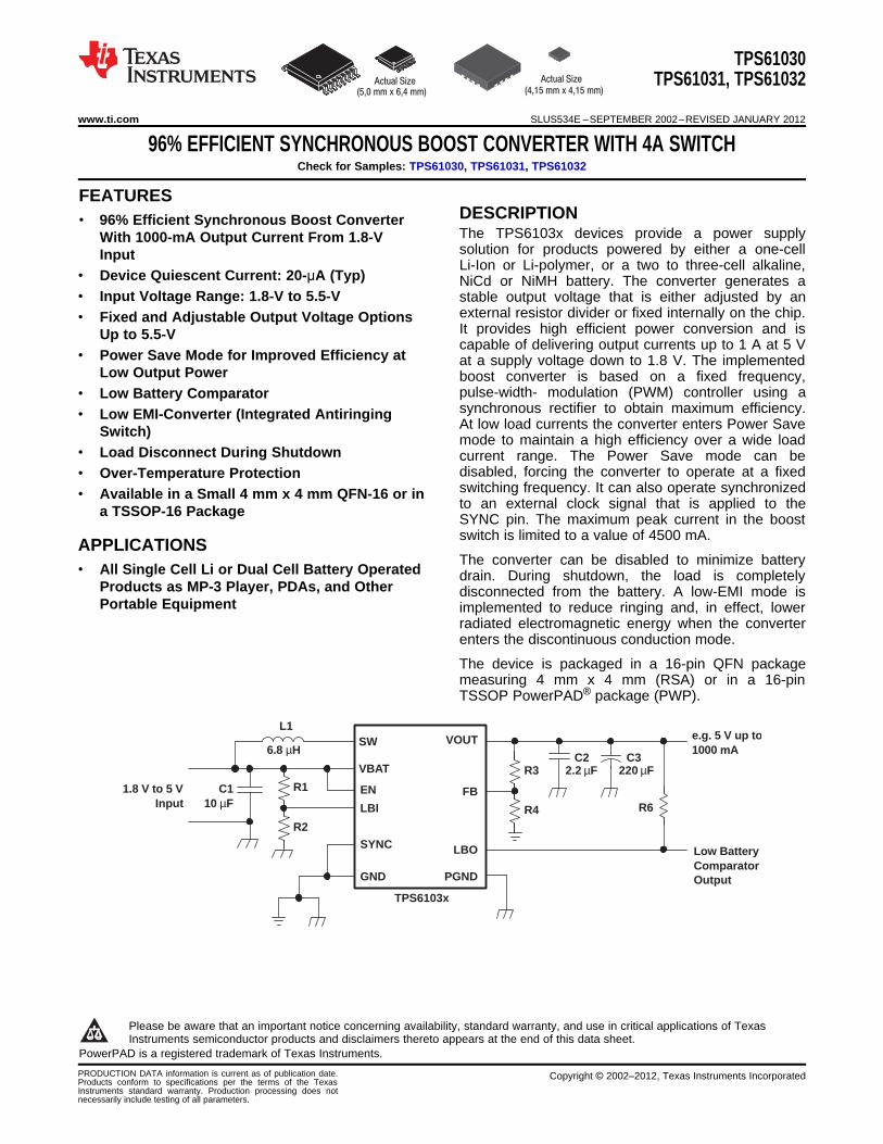
SW
C110 µF
L1
6.8 µH
R1
R2
VBAT
VOUT
FB
C22.2 µF
C3220 µF
LBO
PGND
LBI
SYNC
EN
GND
TPS6103x
e.g. 5 V up to1000 mA
Low BatteryComparatorOutput
R3
R4 R6
1.8 V to 5 VInput
TPS61030TPS61031, TPS61032
www.ti.com SLUS534E –SEPTEMBER 2002–REVISED JANUARY 2012
96% EFFICIENT SYNCHRONOUS BOOST CONVERTER WITH 4A SWITCHCheck for Samples: TPS61030, TPS61031, TPS61032
1FEATURESDESCRIPTION
2• 96% Efficient Synchronous Boost ConverterThe TPS6103x devices provide a power supplyWith 1000-mA Output Current From 1.8-Vsolution for products powered by either a one-cellInputLi-Ion or Li-polymer, or a two to three-cell alkaline,
• Device Quiescent Current: 20-µA (Typ) NiCd or NiMH battery. The converter generates a• Input Voltage Range: 1.8-V to 5.5-V stable output voltage that is either adjusted by an
external resistor divider or fixed internally on the chip.• Fixed and Adjustable Output Voltage OptionsIt provides high efficient power conversion and isUp to 5.5-Vcapable of delivering output currents up to 1 A at 5 V
• Power Save Mode for Improved Efficiency at at a supply voltage down to 1.8 V. The implementedLow Output Power boost converter is based on a fixed frequency,
pulse-width- modulation (PWM) controller using a• Low Battery Comparatorsynchronous rectifier to obtain maximum efficiency.• Low EMI-Converter (Integrated AntiringingAt low load currents the converter enters Power SaveSwitch)mode to maintain a high efficiency over a wide load
• Load Disconnect During Shutdown current range. The Power Save mode can bedisabled, forcing the converter to operate at a fixed• Over-Temperature Protectionswitching frequency. It can also operate synchronized• Available in a Small 4 mm x 4 mm QFN-16 or into an external clock signal that is applied to thea TSSOP-16 Package SYNC pin. The maximum peak current in the boostswitch is limited to a value of 4500 mA.
APPLICATIONSThe converter can be disabled to minimize battery• All Single Cell Li or Dual Cell Battery Operated drain. During shutdown, the load is completely
Products as MP-3 Player, PDAs, and Other disconnected from the battery. A low-EMI mode isPortable Equipment implemented to reduce ringing and, in effect, lower
radiated electromagnetic energy when the converterenters the discontinuous conduction mode.
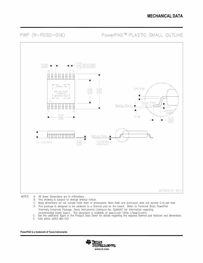
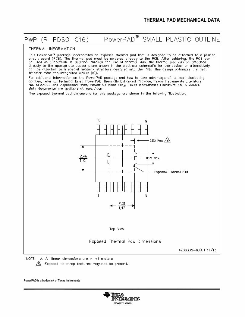
The device is packaged in a 16-pin QFN packagemeasuring 4 mm x 4 mm (RSA) or in a 16-pinTSSOP PowerPAD® package (PWP).
1
Please be aware that an important notice concerning availability, standard warranty, and use in critical applications of TexasInstruments semiconductor products and disclaimers thereto appears at the end of this data sheet.
2PowerPAD is a registered trademark of Texas Instruments.
PRODUCTION DATA information is current as of publication date. Copyright © 2002–2012, Texas Instruments IncorporatedProducts conform to specifications per the terms of the TexasInstruments standard warranty. Production processing does notnecessarily include testing of all parameters.
TPS61030TPS61031, TPS61032
SLUS534E –SEPTEMBER 2002–REVISED JANUARY 2012 www.ti.com
These devices have limited built-in ESD protection. The leads should be shorted together or the device placed in conductive foamduring storage or handling to prevent electrostatic damage to the MOS gates.
AVAILABLE OUTPUT VOLTAGE OPTIONS (1)
OUTPUT VOLTAGETA PACKAGE PART NUMBER (2)DC/DC
Adjustable TPS61030PWP
3.3 V 16-Pin TSSOP PowerPAD™ TPS61031PWP
5 V TPS61032PWP-40°C to 85°C
Adjustable TPS61030RSA
3.3 V 16-Pin QFN TPS61031RSA
5 V TPS61032RSA
(1) Contact the factory to check availability of other fixed output voltage versions.(2) The packages are available taped and reeled. Add R suffix to device type (e.g., TPS61030PWPR or TPS61030RSAR) to order
quantities of 2000 devices per reel for the PWP packaged devices and 3000 units per reel for the RSA package.
ABSOLUTE MAXIMUM RATINGSover operating free-air temperature range (unless otherwise noted) (1)
TPS6103x
Input voltage range on LBI -0.3 V to 3.6 V
Input voltage range on SW, VOUT, LBO, VBAT, SYNC, EN, FB -0.3 V to 7 V
Maximum junction temperature TJ -40°C to 150°CStorage temperature range Tstg -65°C to 150°C
(1) Stresses beyond those listed under Absolute Maximum Ratings may cause permanent damage to the device. These are stress ratingsonly, and functional operation of the device at these or any other conditions beyond those indicated under Recommended OperatingConditions is not implied. Exposure to absolute-maximum-rated conditions for extended periods may affect device reliability.
Recommended Operating ConditionsMIN NOM MAX UNIT
Supply voltage at VBAT, VI 1.8 5.5 V
Operating ambient temperature range, TA -40 85 °COperating virtual junction temperaturerange, TJ -40 125 °C
2 Copyright © 2002–2012, Texas Instruments Incorporated
TPS61030TPS61031, TPS61032
www.ti.com SLUS534E –SEPTEMBER 2002–REVISED JANUARY 2012
electrical characteristicsover recommended free-air temperature range and over recommended input voltage range (typical at an ambient temperaturerange of 25°C) (unless otherwise noted)
DC/DC STAGE
PARAMETER TEST CONDITIONS MIN TYP MAX UNIT
VI Input voltage range 1.8 5.5 V
VO TPS61030 output voltage range 1.8 5.5 V
VFB TPS61030 feedback voltage 490 500 510 mV
f Oscillator frequency 500 600 700 kHz
Frequency range for synchronization 500 700 kHz
Switch current limit VOUT= 5 V 3600 4000 4500 mA
Start-up current limit 0.4 x ISW mA
SWN switch on resistance VOUT= 5 V 55 mΩSWP switch on resistance VOUT= 5 V 55 mΩTotal accuracy -3% 3%
Line regulation 0.6%
Load regulation 0.6%
IO = 0 mA, VEN = VBAT = 1.8 V,VBAT 10 25 µAVOUT =5 VQuiescent current
IO = 0 mA, VEN = VBAT = 1.8 V,VOUT 10 20 µAVOUT = 5 V
Shutdown current VEN= 0 V, VBAT = 2.4 V 0.1 1 µA
CONTROL STAGE
PARAMETER TEST CONDITIONS MIN TYP MAX UNIT
VUVLO Under voltage lockout threshold VLBI voltage decreasing 1.5 V
VIL LBI voltage threshold VLBI voltage decreasing 490 500 510 mV
LBI input hysteresis 10 mV
LBI input current EN = VBAT or GND 0.01 0.1 µA
LBO output low voltage VO = 3.3 V, IOI = 100 µA 0.04 0.4 V
LBO output low current 100 µA
LBO output leakage current VLBO= 7 V 0.01 0.1 µA
VIL EN, SYNC input low voltage 0.2 × VBAT V
VIH EN, SYNC input high voltage 0.8 × VBAT V
EN, SYNC input current Clamped on GND or VBAT 0.01 0.1 µA
Overtemperature protection 140 °COvertemperature hysteresis 20 °C
Copyright © 2002–2012, Texas Instruments Incorporated 3
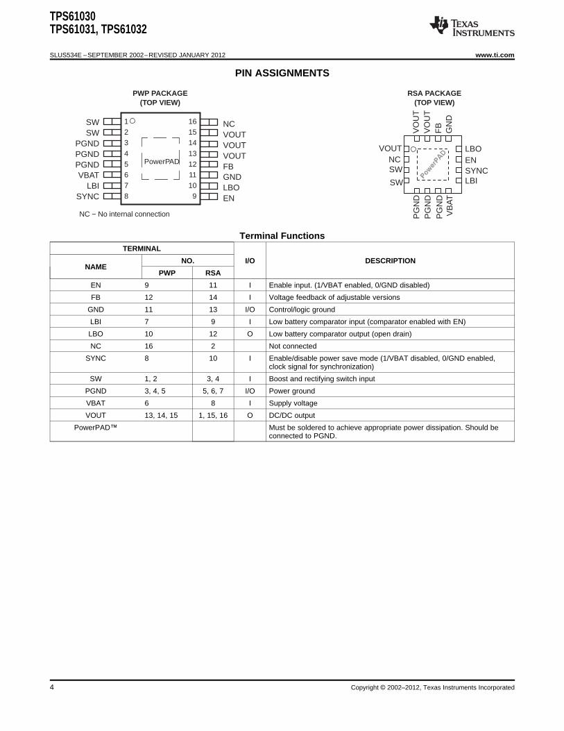
NCSW
SW LBI
LBOVOUT
SYNCEN
PG
ND
PG
ND
PG
ND
VB
AT
VO
UT
VO
UT
FB
GN
D
RSA PACKAGE(TOP VIEW)
123
4 5678
161514
131211109
SWSW
PGNDPGNDPGNDVBAT
LBISYNC
NCVOUTVOUTVOUTFBGNDLBOEN
PWP PACKAGE(TOP VIEW)
NC − No internal connection
PowerPAD
TPS61030TPS61031, TPS61032
SLUS534E –SEPTEMBER 2002–REVISED JANUARY 2012 www.ti.com
PIN ASSIGNMENTS
Terminal FunctionsTERMINAL
NO. I/O DESCRIPTIONNAME
PWP RSA
EN 9 11 I Enable input. (1/VBAT enabled, 0/GND disabled)
FB 12 14 I Voltage feedback of adjustable versions
GND 11 13 I/O Control/logic ground
LBI 7 9 I Low battery comparator input (comparator enabled with EN)
LBO 10 12 O Low battery comparator output (open drain)
NC 16 2 Not connected
SYNC 8 10 I Enable/disable power save mode (1/VBAT disabled, 0/GND enabled,clock signal for synchronization)
SW 1, 2 3, 4 I Boost and rectifying switch input
PGND 3, 4, 5 5, 6, 7 I/O Power ground
VBAT 6 8 I Supply voltage
VOUT 13, 14, 15 1, 15, 16 O DC/DC output
PowerPAD™ Must be soldered to achieve appropriate power dissipation. Should beconnected to PGND.
4 Copyright © 2002–2012, Texas Instruments Incorporated
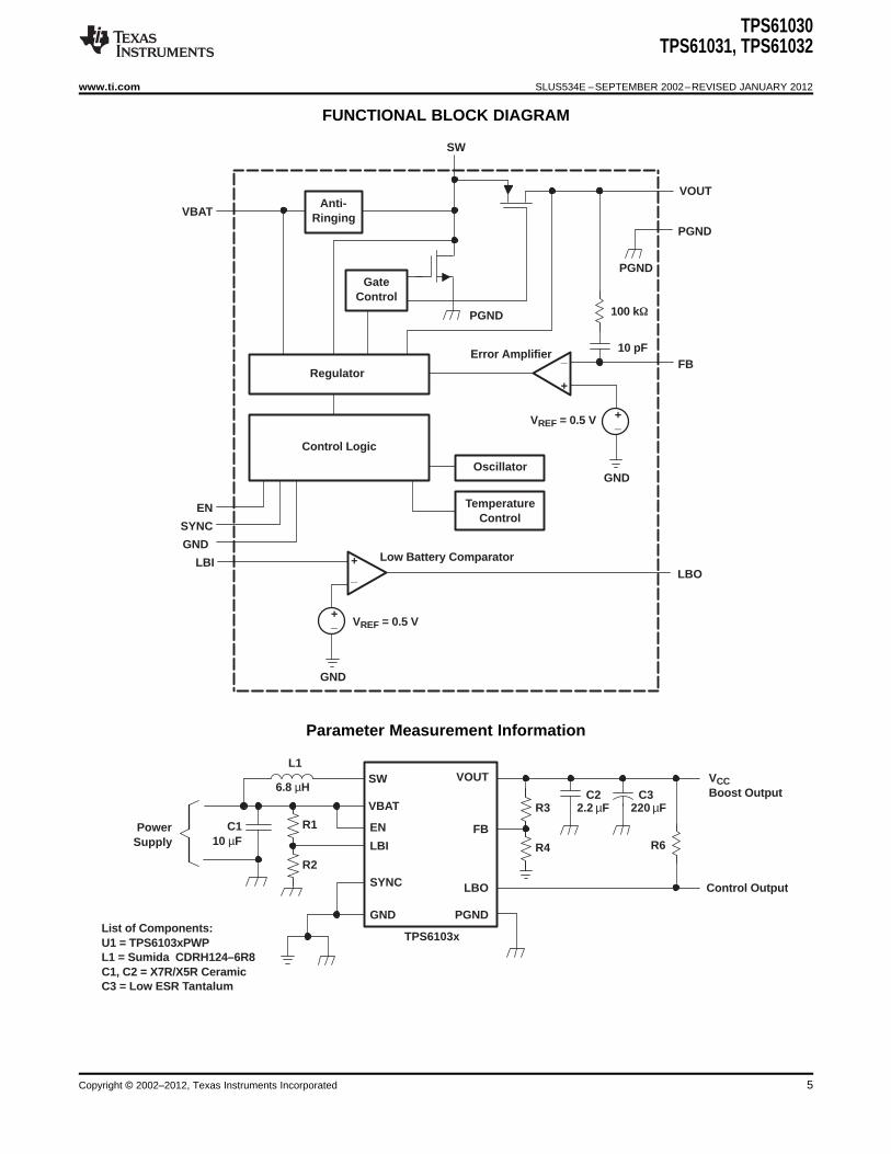
Anti-Ringing
GateControl
PGND
Regulator
PGND
Control Logic
Oscillator
TemperatureControl
VOUT
PGND
FB
SW
VBAT
EN
SYNC
GND
LBILBO
_
+
100 k
10 pF
_+VREF = 0.5 V
GND
Error Amplifier
_+
_+
GND
VREF = 0.5 V
Low Battery Comparator
SW
C110 µF
PowerSupply
L1
6.8 µH
R1
R2
VBAT
VOUT
FB
C22.2 µF
C3220 µF
LBO
PGND
LBI
SYNC
EN
GND
TPS6103xList of Components:U1 = TPS6103xPWPL1 = Sumida CDRH124–6R8C1, C2 = X7R/X5R CeramicC3 = Low ESR Tantalum
VCCBoost Output
Control Output
R3
R4 R6
TPS61030TPS61031, TPS61032
www.ti.com SLUS534E –SEPTEMBER 2002–REVISED JANUARY 2012
FUNCTIONAL BLOCK DIAGRAM
Parameter Measurement Information
Copyright © 2002–2012, Texas Instruments Incorporated 5
0
0.5
1
1.5
2
2.5
3
3.5
1.8 2.2 2.6 3 3.4 3.8 4.2 4.6 5
VI - Input Voltage - V
Max
imu
m O
utp
ut C
urr
ent
- A
0
0.5
1
1.5
2
2.5
3
3.5
1.8 2.2 2.6 3 3.4 3.8 4.2 4.6 5
VI - Input Voltage - V
Max
imu
m O
utp
ut C
urr
ent
- A
TPS61030TPS61031, TPS61032
SLUS534E –SEPTEMBER 2002–REVISED JANUARY 2012 www.ti.com
TYPICAL CHARACTERISTICS
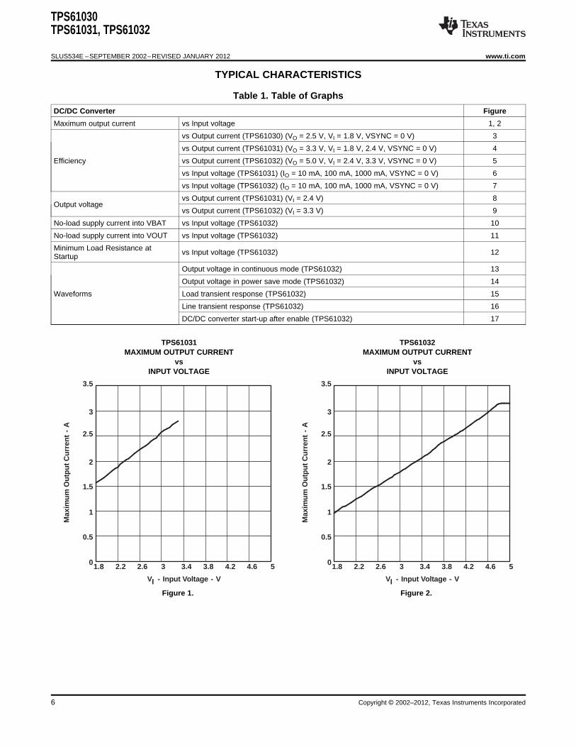
Table 1. Table of Graphs
DC/DC Converter Figure
Maximum output current vs Input voltage 1, 2
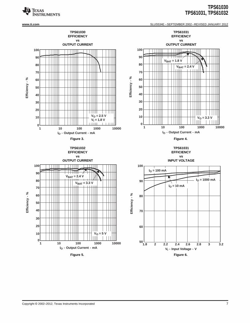
vs Output current (TPS61030) (VO = 2.5 V, VI = 1.8 V, VSYNC = 0 V) 3
vs Output current (TPS61031) (VO = 3.3 V, VI = 1.8 V, 2.4 V, VSYNC = 0 V) 4
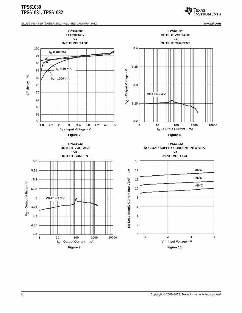
Efficiency vs Output current (TPS61032) (VO = 5.0 V, VI = 2.4 V, 3.3 V, VSYNC = 0 V) 5
vs Input voltage (TPS61031) (IO = 10 mA, 100 mA, 1000 mA, VSYNC = 0 V) 6
vs Input voltage (TPS61032) (IO = 10 mA, 100 mA, 1000 mA, VSYNC = 0 V) 7
vs Output current (TPS61031) (VI = 2.4 V) 8Output voltage
vs Output current (TPS61032) (VI = 3.3 V) 9
No-load supply current into VBAT vs Input voltage (TPS61032) 10
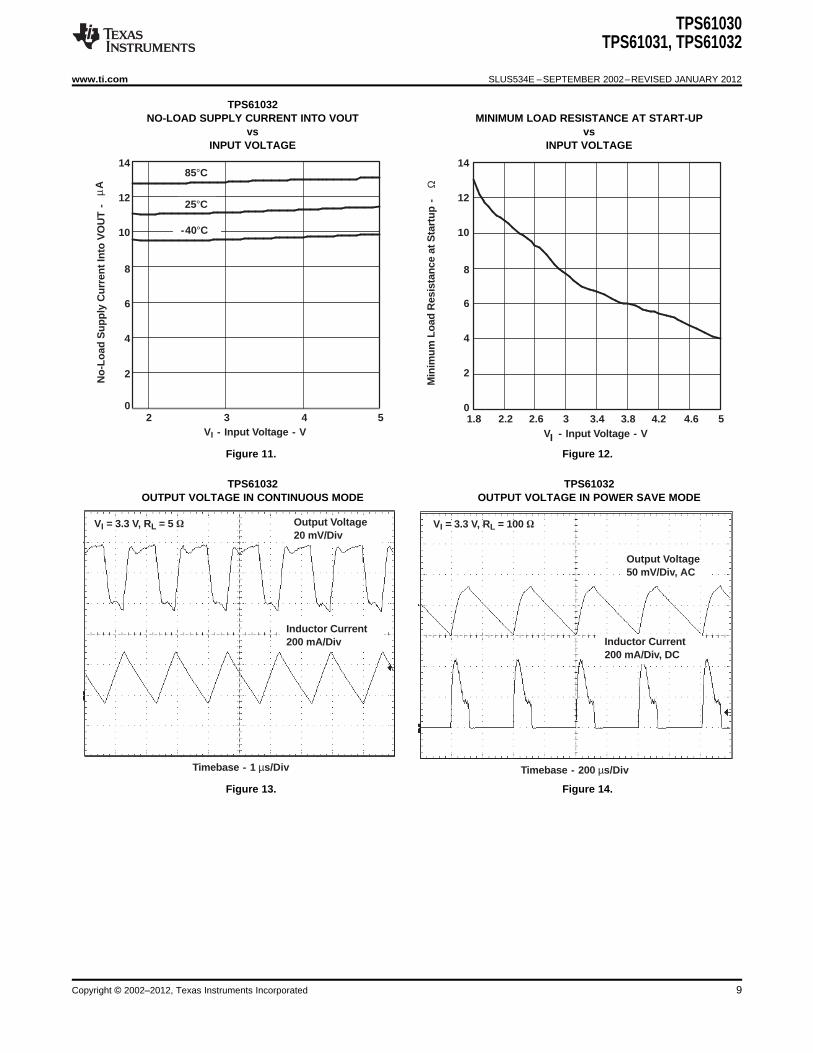
No-load supply current into VOUT vs Input voltage (TPS61032) 11
Minimum Load Resistance at vs Input voltage (TPS61032) 12Startup
Output voltage in continuous mode (TPS61032) 13
Output voltage in power save mode (TPS61032) 14
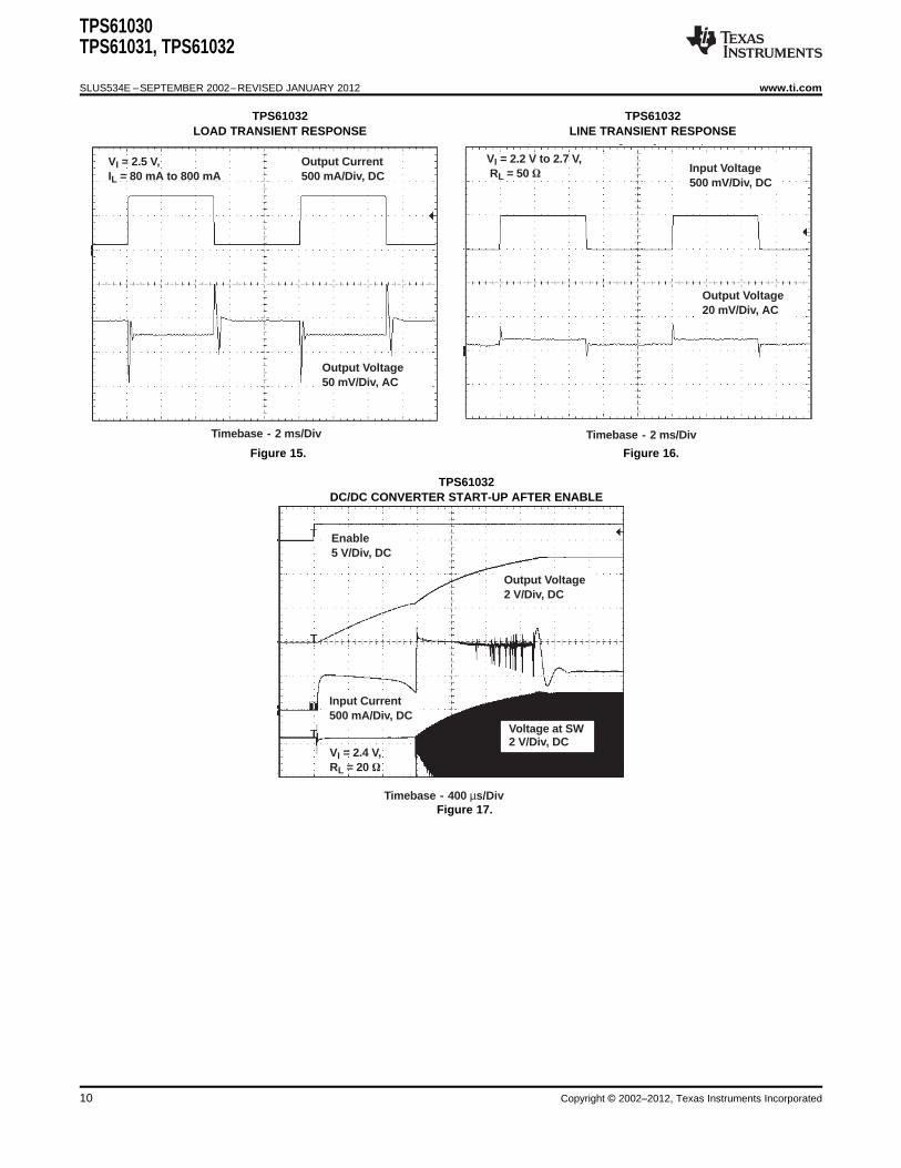
Waveforms Load transient response (TPS61032) 15
Line transient response (TPS61032) 16
DC/DC converter start-up after enable (TPS61032) 17
TPS61031 TPS61032MAXIMUM OUTPUT CURRENT MAXIMUM OUTPUT CURRENT
vs vsINPUT VOLTAGE INPUT VOLTAGE
Figure 1. Figure 2.
6 Copyright © 2002–2012, Texas Instruments Incorporated
0
10
20
30
40
50
60
70
80
90
100
1 10 100 1000 10000
VBAT = 2.4 V
VBAT = 1.8 V
VO = 3.3 V
Eff
icie
ncy
- %
IO - Output Current - mA
0
10
20
30
40
50
60
70
80
90
100
1 10 100 1000 10000
Eff
icie
ncy
- %
IO - Output Current - mA
VO = 2.5 VVI = 1.8 V
0
10
20
30
40
50
60
70
80
90
100
1 10 100 1000 10000
VBAT = 3.3 V
VBAT = 2.4 V
VO = 5 V
Eff
icie
ncy
- %
IO - Output Current - mA
50
80
90
100
Eff
icie
ncy
- %
VI - Input Voltage - V
IO = 10 mA
IO = 100 mA
1.8 2 2.6 2.8 32.2 2.4 3.2
60
IO = 1000 mA
70
TPS61030TPS61031, TPS61032
www.ti.com SLUS534E –SEPTEMBER 2002–REVISED JANUARY 2012
TPS61030 TPS61031EFFICIENCY EFFICIENCY
vs vsOUTPUT CURRENT OUTPUT CURRENT
Figure 3. Figure 4.
TPS61032 TPS61031EFFICIENCY EFFICIENCY
vs vsOUTPUT CURRENT INPUT VOLTAGE
Figure 5. Figure 6.
Copyright © 2002–2012, Texas Instruments Incorporated 7
3.2
3.25
3.3
3.35
3.4
1 10 100 1000 10000-
Ou
tpu
t V
olta
ge
- V
IO - Output Current - mAV
O
VBAT = 2.4 V
50
55
60
65
70
75
80
85
90
95
100
1.8 2.2 2.6 3 3.4 3.8 4.2 4.6 5
Eff
icie
ncy
- %
VI - Input Voltage - V
IO = 100 mA
IO = 10 mA
IO = 1000 mA
4.8
4.85
4.9
4.95
5
5.05
5.1
5.15
5.2
1 10 100 1000 10000
- O
utp
ut
Vo
ltag
e -
V
IO - Output Current - mA
VO
VBAT = 3.3 V
0
2
4
6
8
10
12
14
16
2 3 4 5
VI - Input Voltage - V
-40°C
85°C
25°C
Aµ
No
-Lo
ad S
up
ply
Cu
rren
t In
to V
BA
T -
TPS61030TPS61031, TPS61032
SLUS534E –SEPTEMBER 2002–REVISED JANUARY 2012 www.ti.com
TPS61032 TPS61031EFFICIENCY OUTPUT VOLTAGE
vs vsINPUT VOLTAGE OUTPUT CURRENT
Figure 7. Figure 8.
TPS61032 TPS61032OUTPUT VOLTAGE NO-LOAD SUPPLY CURRENT INTO VBAT
vs vsOUTPUT CURRENT INPUT VOLTAGE
Figure 9. Figure 10.
8 Copyright © 2002–2012, Texas Instruments Incorporated
0
2
4
6
8
10
12
14
2 3 4 5VI - Input Voltage - V
-40°C
85°C
25°C
Aµ
No
-Lo
ad S
up
ply
Cu
rren
t In
to V
OU
T -
0
2
4
6
8
10
12
14
1.8 2.2 2.6 3 3.4 3.8 4.2 4.6 5VI - Input Voltage - V
Min
imu
m L
oad
Res
ista
nce
at S
tart
up
-
Ω
Inductor Current200 mA/Div
Output Voltage20 mV/Div
Timebase - 1 µs/Div
VI = 3.3 V, RL = 5
Inductor Current200 mA/Div, DC
Output Voltage50 mV/Div, AC
Timebase - 200 µs/Div
VI = 3.3 V, RL = 100
TPS61030TPS61031, TPS61032
www.ti.com SLUS534E –SEPTEMBER 2002–REVISED JANUARY 2012
TPS61032NO-LOAD SUPPLY CURRENT INTO VOUT MINIMUM LOAD RESISTANCE AT START-UP
vs vsINPUT VOLTAGE INPUT VOLTAGE
Figure 11. Figure 12.
TPS61032 TPS61032OUTPUT VOLTAGE IN CONTINUOUS MODE OUTPUT VOLTAGE IN POWER SAVE MODE
Figure 13. Figure 14.
Copyright © 2002–2012, Texas Instruments Incorporated 9
Output Voltage50 mV/Div, AC
Output Current500 mA/Div, DC
Timebase - 2 ms/Div
VI = 2.5 V, IL = 80 mA to 800 mA
Output Voltage20 mV/Div, AC
Input Voltage500 mV/Div, DC
Timebase - 2 ms/Div
VI = 2.2 V to 2.7 V, RL = 50
Output Voltage2 V/Div, DC
Input Current500 mA/Div, DC
Enable5 V/Div, DC
Voltage at SW2 V/Div, DC
Timebase - 400 µs/Div
VI = 2.4 V,RL = 20
TPS61030TPS61031, TPS61032
SLUS534E –SEPTEMBER 2002–REVISED JANUARY 2012 www.ti.com
TPS61032 TPS61032LOAD TRANSIENT RESPONSE LINE TRANSIENT RESPONSE
Figure 15. Figure 16.
TPS61032DC/DC CONVERTER START-UP AFTER ENABLE
Figure 17.
10 Copyright © 2002–2012, Texas Instruments Incorporated
TPS61030TPS61031, TPS61032
www.ti.com SLUS534E –SEPTEMBER 2002–REVISED JANUARY 2012
Detailed Description
Controller Circuit
The controller circuit of the device is based on a fixed frequency multiple feedforward controller topology. Inputvoltage, output voltage, and voltage drop on the NMOS switch are monitored and forwarded to the regulator. Sochanges in the operating conditions of the converter directly affect the duty cycle and must not take the indirectand slow way through the control loop and the error amplifier. The control loop, determined by the error amplifier,only has to handle small signal errors. The input for it is the feedback voltage on the FB pin or, at fixed outputvoltage versions, the voltage on the internal resistor divider. It is compared with the internal reference voltage togenerate an accurate and stable output voltage.
The peak current of the NMOS switch is also sensed to limit the maximum current flowing through the switch andthe inductor. The typical peak current limit is set to 4000 mA. An internal temperature sensor prevents the devicefrom getting overheated in case of excessive power dissipation.
Synchronous Rectifier
The device integrates an N-channel and a P-channel MOSFET transistor to realize a synchronous rectifier.Because the commonly used discrete Schottky rectifier is replaced with a low RDS(ON) PMOS switch, the powerconversion efficiency reaches 96%. To avoid ground shift due to the high currents in the NMOS switch, twoseparate ground pins are used. The reference for all control functions is the GND pin. The source of the NMOSswitch is connected to PGND. Both grounds must be connected on the PCB at only one point close to the GNDpin. A special circuit is applied to disconnect the load from the input during shutdown of the converter. Inconventional synchronous rectifier circuits, the backgate diode of the high-side PMOS is forward biased inshutdown and allows current flowing from the battery to the output. This device however uses a special circuitwhich takes the cathode of the backgate diode of the high-side PMOS and disconnects it from the source whenthe regulator is not enabled (EN = low).
The benefit of this feature for the system design engineer is that the battery is not depleted during shutdown ofthe converter. No additional components have to be added to the design to make sure that the battery isdisconnected from the output of the converter.
Device Enable
The device is put into operation when EN is set high. It is put into a shutdown mode when EN is set to GND. Inshutdown mode, the regulator stops switching, all internal control circuitry including the low-battery comparator isswitched off, and the load is isolated from the input (as described in the Synchronous Rectifier Section). Thisalso means that the output voltage can drop below the input voltage during shutdown. During start-up of theconverter, the duty cycle and the peak current are limited in order to avoid high peak currents drawn from thebattery.
Undervoltage Lockout
An undervoltage lockout function prevents device start-up if the supply voltage on VBAT is lower thanapproximately 1.6 V. When in operation and the battery is being discharged, the device automatically enters theshutdown mode if the voltage on VBAT drops below approximately 1.6 V. This undervoltage lockout function isimplemented in order to prevent the malfunctioning of the converter.
Softstart
When the device enables the internal start-up cycle starts with the first step, the precharge phase. Duringprecharge, the rectifying switch is turned on until the output capacitor is charged to a value close to the inputvoltage. The rectifying switch current is limited in that phase. This also limits the output current under short-circuitconditions at the output. After charging the output capacitor to the input voltage the device starts switching. Untilthe output voltage is reached, the boost switch current limit is set to 40% of its nominal value to avoid high peakcurrents at the battery during startup. When the output voltage is reached, the regulator takes control and theswitch current limit is set back to 100%.
Copyright © 2002–2012, Texas Instruments Incorporated 11
TPS61030TPS61031, TPS61032
SLUS534E –SEPTEMBER 2002–REVISED JANUARY 2012 www.ti.com
Power Save Mode and Synchronization
The SYNC pin can be used to select different operation modes. To enable power save, SYNC must be set low.Power save mode is used to improve efficiency at light load. In power save mode the converter only operateswhen the output voltage trips below a set threshold voltage. It ramps up the output voltage with one or severalpulses and goes again into power save mode once the output voltage exceeds the set threshold voltage. Thispower save mode can be disabled by setting the SYNC to VBAT.
Applying an external clock with a duty cycle between 30% and 70% at the SYNC pin forces the converter tooperate at the applied clock frequency. The external frequency has to be in the range of about ±20% of thenominal internal frequency. Detailed values are shown in the electrical characteristic section of the data sheet.
Low Battery Detector Circuit—LBI/LBO
The low-battery detector circuit is typically used to supervise the battery voltage and to generate an error flagwhen the battery voltage drops below a user-set threshold voltage. The function is active only when the device isenabled. When the device is disabled, the LBO pin is high-impedance. The switching threshold is 500 mV at LBI.During normal operation, LBO stays at high impedance when the voltage, applied at LBI, is above the threshold.It is active low when the voltage at LBI goes below 500 mV.
The battery voltage, at which the detection circuit switches, can be programmed with a resistive dividerconnected to the LBI pin. The resistive divider scales down the battery voltage to a voltage level of 500 mV,which is then compared to the LBI threshold voltage. The LBI pin has a built-in hysteresis of 10 mV. See theapplication section for more details about the programming of the LBI threshold. If the low-battery detectioncircuit is not used, the LBI pin should be connected to GND (or to VBAT) and the LBO pin can be leftunconnected. Do not let the LBI pin float.
Low-EMI Switch
The device integrates a circuit that removes the ringing that typically appears on the SW node when theconverter enters discontinuous current mode. In this case, the current through the inductor ramps to zero and therectifying PMOS switch is turned off to prevent a reverse current flowing from the output capacitors back to thebattery. Due to the remaining energy that is stored in parasitic components of the semiconductor and theinductor, a ringing on the SW pin is induced. The integrated antiringing switch clamps this voltage to VBAT andtherefore dampens ringing.
12 Copyright © 2002–2012, Texas Instruments Incorporated
R3 R4 VOVFB
1 180 k VO500 mV
1
CparR3 10 pF 200 kR4
–1
SW
C1PowerSupply
L1
R1
R2
VBAT
VOUT
FB
C2 C3
LBO
PGND
LBI
SYNC
EN
GND
TPS6103x
VCCBoost Output
Control Output
R3
R4 R6
R1 R2 VBATVLBIthreshold
1 390 k VBAT500 mV
1
TPS61030TPS61031, TPS61032
www.ti.com SLUS534E –SEPTEMBER 2002–REVISED JANUARY 2012
APPLICATION INFORMATION
Design Procedure
The TPS6103x dc/dc converters are intended for systems powered by a dual or triple cell NiCd or NiMH batterywith a typical terminal voltage between 1.8 V and 5.5 V. They can also be used in systems powered by one-cellLi-Ion with a typical stack voltage between 2.5 V and 4.2 V. Additionally, two or three primary and secondaryalkaline battery cells can be the power source in systems where the TPS6103x is used.
Programming the Output Voltage
The output voltage of the TPS61030 dc/dc converter section can be adjusted with an external resistor divider.The typical value of the voltage on the FB pin is 500 mV. The maximum allowed value for the output voltage is5.5 V. The current through the resistive divider should be about 100 times greater than the current into the FBpin. The typical current into the FB pin is 0.01 µA, and the voltage across R6 is typically 500 mV. Based on thosetwo values, the recommended value for R4 should be lower than 500 kΩ, in order to set the divider current at 1µA or higher. Because of internal compensation circuitry the value for this resistor should be in the range of 200kΩ. From that, the value of resistor R3, depending on the needed output voltage (VO), can be calculated usingequation 1:
(1)
If as an example, an output voltage of 3.3 V is needed, a 1-MΩ resistor should be chosen for R3. If for anyreason the value for R4 is chosen significantly lower than 200 kΩ additional capacitance in parallel to R3 isrecommended. The required capacitance value can be easily calculated using Equation 2:
(2)
Figure 18. Typical Application Circuit for Adjustable Output Voltage Option
Programming the LBI/LBO Threshold Voltage
The current through the resistive divider should be about 100 times greater than the current into the LBI pin. Thetypical current into the LBI pin is 0.01 µA, and the voltage across R2 is equal to the LBI voltage threshold that isgenerated on-chip, which has a value of 500 mV. The recommended value for R2 is therefore in the range of 500kΩ. From that, the value of resistor R1, depending on the desired minimum battery voltage VBAT, can becalculated using Equation 3.
(3)
Copyright © 2002–2012, Texas Instruments Incorporated 13
IL IOUT
VOUTVBAT 0.8
L VBAT VOUT–VBAT
IL ƒ VOUT
TPS61030TPS61031, TPS61032
SLUS534E –SEPTEMBER 2002–REVISED JANUARY 2012 www.ti.com
The output of the low battery supervisor is a simple open-drain output that goes active low if the dedicatedbattery voltage drops below the programmed threshold voltage on LBI. The output requires a pullup resistor witha recommended value of 1 MΩ. The maximum voltage which is used to pull up the LBO outputs should notexceed the output voltage of the dc/dc converter. If not used, the LBO pin can be left floating or tied to GND.
Inductor Selection
A boost converter normally requires two main passive components for storing energy during the conversion. Aboost inductor and a storage capacitor at the output are required. To select the boost inductor, it isrecommended to keep the possible peak inductor current below the current limit threshold of the power switch inthe chosen configuration. For example, the current limit threshold of the TPS6103x's switch is 4500 mA at anoutput voltage of 5 V. The highest peak current through the inductor and the switch depends on the output load,the input (VBAT), and the output voltage (VOUT). Estimation of the maximum average inductor current can be doneusing Equation 4:
(4)
For example, for an output current of 1000 mA at 5 V, at least 3500 mA of average current flows through theinductor at a minimum input voltage of 1.8 V.
The second parameter for choosing the inductor is the desired current ripple in the inductor. Normally, it isadvisable to work with a ripple of less than 20% of the average inductor current. A smaller ripple reduces themagnetic hysteresis losses in the inductor, as well as output voltage ripple and EMI. But in the same way,regulation time at load changes rises. In addition, a larger inductor increases the total system costs. With thoseparameters, it is possible to calculate the value for the inductor by using Equation 5:
(5)
Parameter f is the switching frequency and ΔIL is the ripple current in the inductor, i.e., 10% × IL. In this example,the desired inductor has the value of 5.5 µH. In typical applications a 6.8 µH inductance is recommended. Theminimum possible inductance value is 2.2 µH. With the calculated inductance and current values, it is possible tochoose a suitable inductor. Care has to be taken that load transients and losses in the circuit can lead to highercurrents as estimated in equation 4. Also, the losses in the inductor caused by magnetic hysteresis losses andcopper losses are a major parameter for total circuit efficiency.
The following inductor series from different suppliers have been used with the TPS6103x converters:
List of InductorsVENDOR INDUCTOR SERIES
CDRH124
Sumida CDRH103R
CDRH104R
7447779___Wurth Electronik
744771___
EPCOS B82464G
14 Copyright © 2002–2012, Texas Instruments Incorporated
Cmin IOUT VOUT VBAT
ƒ V VOUT
VESR IOUT RESR
AREG d
VFB
5 (R3 R4)R4 (1 i 2.3 s)
TPS61030TPS61031, TPS61032
www.ti.com SLUS534E –SEPTEMBER 2002–REVISED JANUARY 2012
Capacitor Selection
Input Capacitor
At least a 10-µF input capacitor is recommended to improve transient behavior of the regulator and EMI behaviorof the total power supply circuit. A ceramic capacitor or a tantalum capacitor with a 100-nF ceramic capacitor inparallel, placed close to the IC, is recommended.
Output Capacitor
The major parameter necessary to define the output capacitor is the maximum allowed output voltage ripple ofthe converter. This ripple is determined by two parameters of the capacitor, the capacitance and the ESR. It ispossible to calculate the minimum capacitance needed for the defined ripple, supposing that the ESR is zero, byusing Equation 6:
(6)
Parameter f is the switching frequency and ΔV is the maximum allowed ripple.
With a chosen ripple voltage of 10 mV, a minimum capacitance of 100 µF is needed. The total ripple is largerdue to the ESR of the output capacitor. This additional component of the ripple can be calculated usingEquation 7:
(7)
An additional ripple of 80 mV is the result of using a tantalum capacitor with a low ESR of 80 mΩ. The total rippleis the sum of the ripple caused by the capacitance and the ripple caused by the ESR of the capacitor. In thisexample, the total ripple is 90 mV. Additional ripple is caused by load transients. This means that the outputcapacitance needs to be larger than calculated above to meet the total ripple requirements.
The output capacitor must completely supply the load during the charging phase of the inductor. A reasonablevalue of the output capacitance depends on the speed of the load transients and the load current during the loadchange. With the calculated minimum value of 100 µF and load transient considerations, a recommended outputcapacitance value is in around 220 µF. For economical reasons this usually is a tantalum capacitor. Because ofthis the control loop has been optimized for using output capacitors with an ESR of above 30 mΩ. The minimumvalue for the output capacitor is 22 µF.
Small Signal Stability
When using output capacitors with lower ESR, like ceramics, it is recommended to use the adjustable voltageversion. The missing ESR can be easily compensated there in the feedback divider. Typically a capacitor in therange of 10 pF in parallel to R3 helps to obtain small signal stability with lowest ESR output capacitors. For moredetailed analysis the small signal transfer function of the error amplifier and regulator, which is given in Equation8, can be used.
(8)
Layout Considerations
As for all switching power supplies, the layout is an important step in the design, especially at high peak currentsand high switching frequencies. If the layout is not carefully done, the regulator could show stability problems aswell as EMI problems. Therefore, use wide and short traces for the main current path and for the power groundtracks. The input capacitor, output capacitor, and the inductor should be placed as close as possible to the IC.Use a common ground node for power ground and a different one for control ground to minimize the effects ofground noise. Connect these ground nodes at any place close to one of the ground pins of the IC.
The feedback divider should be placed as close as possible to the control ground pin of the IC. To lay out thecontrol ground, it is recommended to use short traces as well, separated from the power ground traces. Thisavoids ground shift problems, which can occur due to superimposition of power ground current and controlground current.
Copyright © 2002–2012, Texas Instruments Incorporated 15
SW
C110 µF
L1
6.8 µH
R1
R2
VBAT
VOUT
FB
C22.2 µF
C3220 µF
LBO
PGND
LBI
SYNC
EN
GND
TPS61032
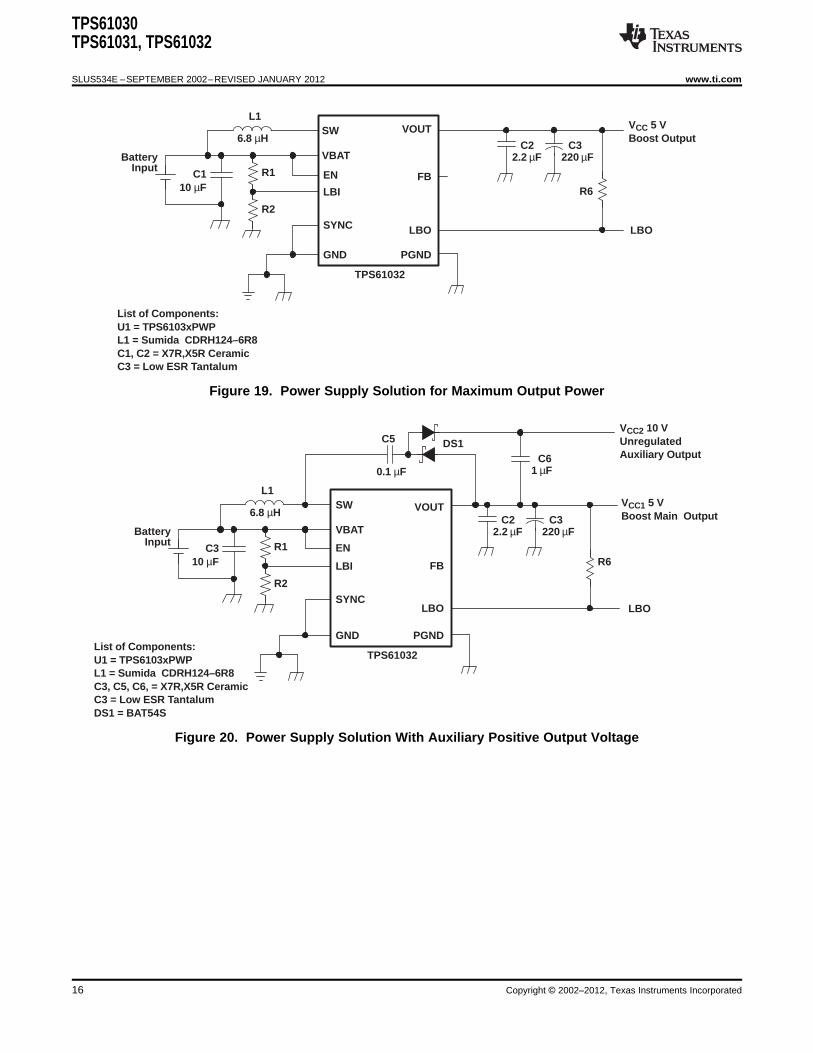
List of Components:U1 = TPS6103xPWPL1 = Sumida CDRH124–6R8C1, C2 = X7R,X5R CeramicC3 = Low ESR Tantalum
VCC 5 VBoost Output
LBO
R6
BatteryInput
SW
C310 µF
L1
6.8 µH
R1
R2
VBAT
VOUT
R6
C22.2 µF
C3220 µF
LBO
PGND
LBI
SYNC
EN
GND
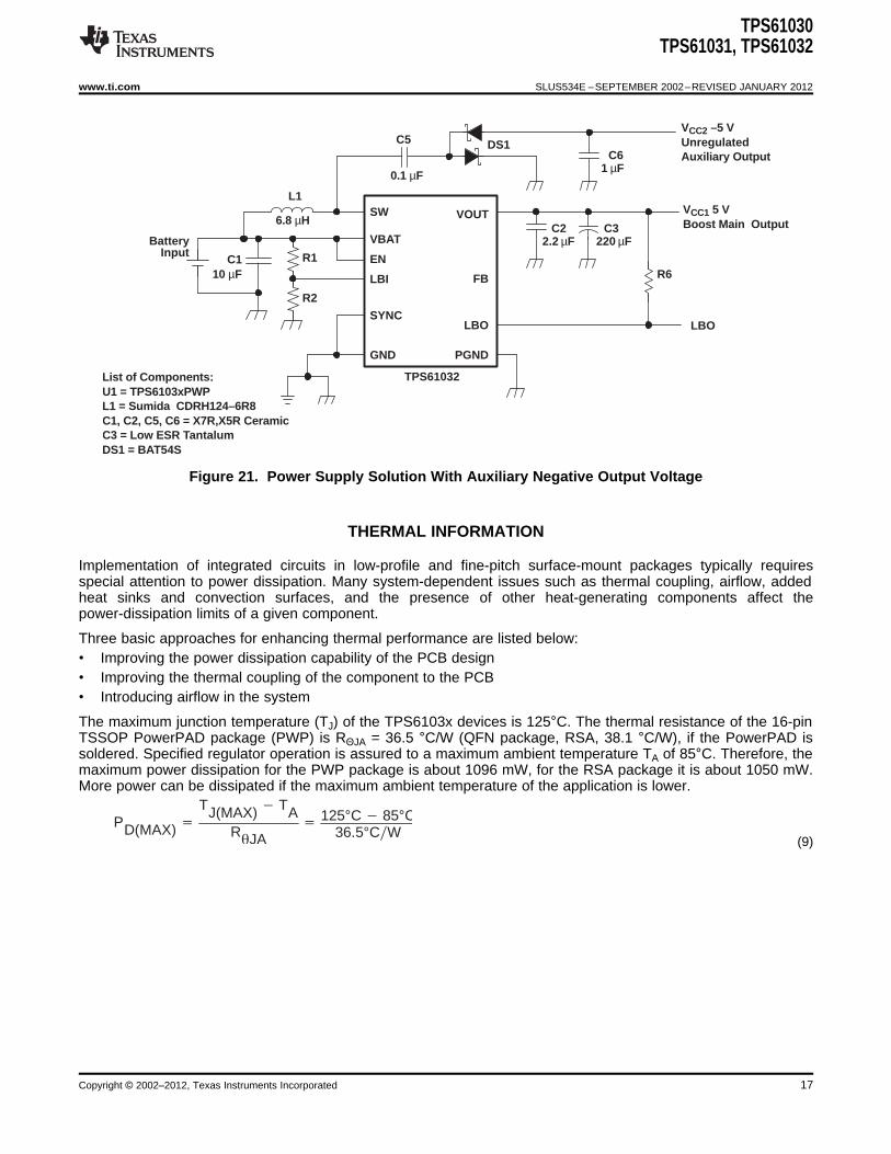
TPS61032List of Components:U1 = TPS6103xPWPL1 = Sumida CDRH124–6R8C3, C5, C6, = X7R,X5R CeramicC3 = Low ESR TantalumDS1 = BAT54S
LBO
C5
0.1 µF
DS1C6
1 µF
VCC2 10 VUnregulatedAuxiliary Output
BatteryInput
FB
VCC1 5 VBoost Main Output
TPS61030TPS61031, TPS61032
SLUS534E –SEPTEMBER 2002–REVISED JANUARY 2012 www.ti.com
Figure 19. Power Supply Solution for Maximum Output Power
Figure 20. Power Supply Solution With Auxiliary Positive Output Voltage
16 Copyright © 2002–2012, Texas Instruments Incorporated
SW
C110 µF
L1
6.8 µH
R1
R2
VBAT
VOUT
R6
C22.2 µF
C3220 µF
LBO
PGND
LBI
SYNC
EN
GND
TPS61032List of Components:U1 = TPS6103xPWPL1 = Sumida CDRH124–6R8C1, C2, C5, C6 = X7R,X5R CeramicC3 = Low ESR TantalumDS1 = BAT54S
LBO
C5
0.1 µF
DS1C6
1 µF
VCC2 –5 VUnregulatedAuxiliary Output
BatteryInput
FB
VCC1 5 VBoost Main Output
PD(MAX) TJ(MAX) TA
RJA
125°C 85°C36.5°CW
TPS61030TPS61031, TPS61032
www.ti.com SLUS534E –SEPTEMBER 2002–REVISED JANUARY 2012
Figure 21. Power Supply Solution With Auxiliary Negative Output Voltage
THERMAL INFORMATION
Implementation of integrated circuits in low-profile and fine-pitch surface-mount packages typically requiresspecial attention to power dissipation. Many system-dependent issues such as thermal coupling, airflow, addedheat sinks and convection surfaces, and the presence of other heat-generating components affect thepower-dissipation limits of a given component.
Three basic approaches for enhancing thermal performance are listed below:• Improving the power dissipation capability of the PCB design• Improving the thermal coupling of the component to the PCB• Introducing airflow in the system
The maximum junction temperature (TJ) of the TPS6103x devices is 125°C. The thermal resistance of the 16-pinTSSOP PowerPAD package (PWP) is RΘJA = 36.5 °C/W (QFN package, RSA, 38.1 °C/W), if the PowerPAD issoldered. Specified regulator operation is assured to a maximum ambient temperature TA of 85°C. Therefore, themaximum power dissipation for the PWP package is about 1096 mW, for the RSA package it is about 1050 mW.More power can be dissipated if the maximum ambient temperature of the application is lower.
(9)
Copyright © 2002–2012, Texas Instruments Incorporated 17
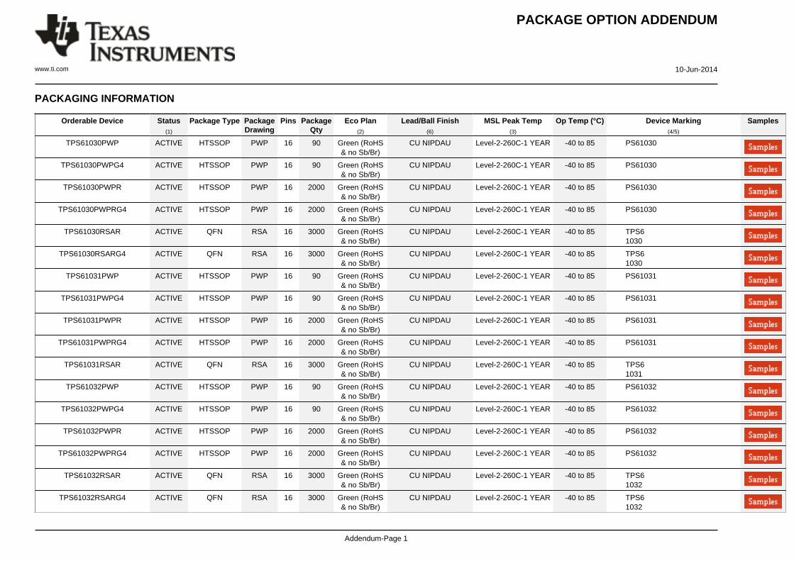
PACKAGE OPTION ADDENDUM
www.ti.com 10-Jun-2014
Addendum-Page 1
PACKAGING INFORMATION
Orderable Device Status(1)
Package Type PackageDrawing
Pins PackageQty
Eco Plan(2)
Lead/Ball Finish(6)
MSL Peak Temp(3)
Op Temp (°C) Device Marking(4/5)
Samples
TPS61030PWP ACTIVE HTSSOP PWP 16 90 Green (RoHS& no Sb/Br)
CU NIPDAU Level-2-260C-1 YEAR -40 to 85 PS61030
TPS61030PWPG4 ACTIVE HTSSOP PWP 16 90 Green (RoHS& no Sb/Br)
CU NIPDAU Level-2-260C-1 YEAR -40 to 85 PS61030
TPS61030PWPR ACTIVE HTSSOP PWP 16 2000 Green (RoHS& no Sb/Br)
CU NIPDAU Level-2-260C-1 YEAR -40 to 85 PS61030
TPS61030PWPRG4 ACTIVE HTSSOP PWP 16 2000 Green (RoHS& no Sb/Br)
CU NIPDAU Level-2-260C-1 YEAR -40 to 85 PS61030
TPS61030RSAR ACTIVE QFN RSA 16 3000 Green (RoHS& no Sb/Br)
CU NIPDAU Level-2-260C-1 YEAR -40 to 85 TPS61030
TPS61030RSARG4 ACTIVE QFN RSA 16 3000 Green (RoHS& no Sb/Br)
CU NIPDAU Level-2-260C-1 YEAR -40 to 85 TPS61030
TPS61031PWP ACTIVE HTSSOP PWP 16 90 Green (RoHS& no Sb/Br)
CU NIPDAU Level-2-260C-1 YEAR -40 to 85 PS61031
TPS61031PWPG4 ACTIVE HTSSOP PWP 16 90 Green (RoHS& no Sb/Br)
CU NIPDAU Level-2-260C-1 YEAR -40 to 85 PS61031
TPS61031PWPR ACTIVE HTSSOP PWP 16 2000 Green (RoHS& no Sb/Br)
CU NIPDAU Level-2-260C-1 YEAR -40 to 85 PS61031
TPS61031PWPRG4 ACTIVE HTSSOP PWP 16 2000 Green (RoHS& no Sb/Br)
CU NIPDAU Level-2-260C-1 YEAR -40 to 85 PS61031
TPS61031RSAR ACTIVE QFN RSA 16 3000 Green (RoHS& no Sb/Br)
CU NIPDAU Level-2-260C-1 YEAR -40 to 85 TPS61031
TPS61032PWP ACTIVE HTSSOP PWP 16 90 Green (RoHS& no Sb/Br)
CU NIPDAU Level-2-260C-1 YEAR -40 to 85 PS61032
TPS61032PWPG4 ACTIVE HTSSOP PWP 16 90 Green (RoHS& no Sb/Br)
CU NIPDAU Level-2-260C-1 YEAR -40 to 85 PS61032
TPS61032PWPR ACTIVE HTSSOP PWP 16 2000 Green (RoHS& no Sb/Br)
CU NIPDAU Level-2-260C-1 YEAR -40 to 85 PS61032
TPS61032PWPRG4 ACTIVE HTSSOP PWP 16 2000 Green (RoHS& no Sb/Br)
CU NIPDAU Level-2-260C-1 YEAR -40 to 85 PS61032
TPS61032RSAR ACTIVE QFN RSA 16 3000 Green (RoHS& no Sb/Br)
CU NIPDAU Level-2-260C-1 YEAR -40 to 85 TPS61032
TPS61032RSARG4 ACTIVE QFN RSA 16 3000 Green (RoHS& no Sb/Br)
CU NIPDAU Level-2-260C-1 YEAR -40 to 85 TPS61032
PACKAGE OPTION ADDENDUM
www.ti.com 10-Jun-2014
Addendum-Page 2
(1) The marketing status values are defined as follows:ACTIVE: Product device recommended for new designs.LIFEBUY: TI has announced that the device will be discontinued, and a lifetime-buy period is in effect.NRND: Not recommended for new designs. Device is in production to support existing customers, but TI does not recommend using this part in a new design.PREVIEW: Device has been announced but is not in production. Samples may or may not be available.OBSOLETE: TI has discontinued the production of the device.
(2) Eco Plan - The planned eco-friendly classification: Pb-Free (RoHS), Pb-Free (RoHS Exempt), or Green (RoHS & no Sb/Br) - please check http://www.ti.com/productcontent for the latest availabilityinformation and additional product content details.TBD: The Pb-Free/Green conversion plan has not been defined.Pb-Free (RoHS): TI's terms "Lead-Free" or "Pb-Free" mean semiconductor products that are compatible with the current RoHS requirements for all 6 substances, including the requirement thatlead not exceed 0.1% by weight in homogeneous materials. Where designed to be soldered at high temperatures, TI Pb-Free products are suitable for use in specified lead-free processes.Pb-Free (RoHS Exempt): This component has a RoHS exemption for either 1) lead-based flip-chip solder bumps used between the die and package, or 2) lead-based die adhesive used betweenthe die and leadframe. The component is otherwise considered Pb-Free (RoHS compatible) as defined above.Green (RoHS & no Sb/Br): TI defines "Green" to mean Pb-Free (RoHS compatible), and free of Bromine (Br) and Antimony (Sb) based flame retardants (Br or Sb do not exceed 0.1% by weightin homogeneous material)
(3) MSL, Peak Temp. - The Moisture Sensitivity Level rating according to the JEDEC industry standard classifications, and peak solder temperature.
(4) There may be additional marking, which relates to the logo, the lot trace code information, or the environmental category on the device.
(5) Multiple Device Markings will be inside parentheses. Only one Device Marking contained in parentheses and separated by a "~" will appear on a device. If a line is indented then it is a continuationof the previous line and the two combined represent the entire Device Marking for that device.
(6) Lead/Ball Finish - Orderable Devices may have multiple material finish options. Finish options are separated by a vertical ruled line. Lead/Ball Finish values may wrap to two lines if the finishvalue exceeds the maximum column width.
Important Information and Disclaimer:The information provided on this page represents TI's knowledge and belief as of the date that it is provided. TI bases its knowledge and belief on informationprovided by third parties, and makes no representation or warranty as to the accuracy of such information. Efforts are underway to better integrate information from third parties. TI has taken andcontinues to take reasonable steps to provide representative and accurate information but may not have conducted destructive testing or chemical analysis on incoming materials and chemicals.TI and TI suppliers consider certain information to be proprietary, and thus CAS numbers and other limited information may not be available for release.
In no event shall TI's liability arising out of such information exceed the total purchase price of the TI part(s) at issue in this document sold by TI to Customer on an annual basis.
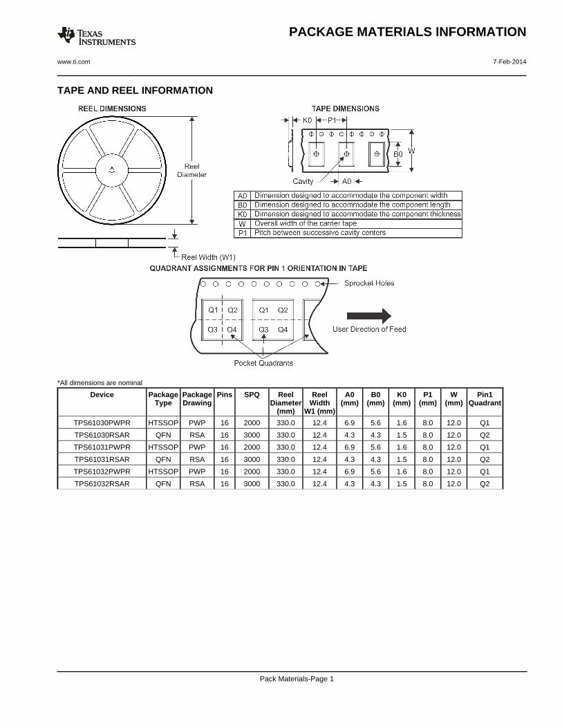
TAPE AND REEL INFORMATION
*All dimensions are nominal
Device PackageType
PackageDrawing
Pins SPQ ReelDiameter
(mm)
ReelWidth
W1 (mm)
A0(mm)
B0(mm)
K0(mm)
P1(mm)
W(mm)
Pin1Quadrant
TPS61030PWPR HTSSOP PWP 16 2000 330.0 12.4 6.9 5.6 1.6 8.0 12.0 Q1
TPS61030RSAR QFN RSA 16 3000 330.0 12.4 4.3 4.3 1.5 8.0 12.0 Q2
TPS61031PWPR HTSSOP PWP 16 2000 330.0 12.4 6.9 5.6 1.6 8.0 12.0 Q1
TPS61031RSAR QFN RSA 16 3000 330.0 12.4 4.3 4.3 1.5 8.0 12.0 Q2
TPS61032PWPR HTSSOP PWP 16 2000 330.0 12.4 6.9 5.6 1.6 8.0 12.0 Q1
TPS61032RSAR QFN RSA 16 3000 330.0 12.4 4.3 4.3 1.5 8.0 12.0 Q2
PACKAGE MATERIALS INFORMATION
www.ti.com 7-Feb-2014
Pack Materials-Page 1
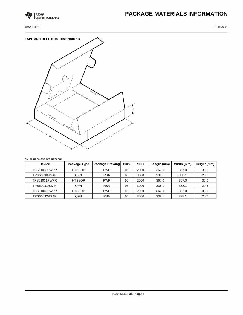
*All dimensions are nominal
Device Package Type Package Drawing Pins SPQ Length (mm) Width (mm) Height (mm)
TPS61030PWPR HTSSOP PWP 16 2000 367.0 367.0 35.0
TPS61030RSAR QFN RSA 16 3000 338.1 338.1 20.6
TPS61031PWPR HTSSOP PWP 16 2000 367.0 367.0 35.0
TPS61031RSAR QFN RSA 16 3000 338.1 338.1 20.6
TPS61032PWPR HTSSOP PWP 16 2000 367.0 367.0 35.0
TPS61032RSAR QFN RSA 16 3000 338.1 338.1 20.6
PACKAGE MATERIALS INFORMATION
www.ti.com 7-Feb-2014
Pack Materials-Page 2
IMPORTANT NOTICETexas Instruments Incorporated and its subsidiaries (TI) reserve the right to make corrections, enhancements, improvements and otherchanges to its semiconductor products and services per JESD46, latest issue, and to discontinue any product or service per JESD48, latestissue. Buyers should obtain the latest relevant information before placing orders and should verify that such information is current andcomplete. All semiconductor products (also referred to herein as “components”) are sold subject to TI’s terms and conditions of salesupplied at the time of order acknowledgment.TI warrants performance of its components to the specifications applicable at the time of sale, in accordance with the warranty in TI’s termsand conditions of sale of semiconductor products. Testing and other quality control techniques are used to the extent TI deems necessaryto support this warranty. Except where mandated by applicable law, testing of all parameters of each component is not necessarilyperformed.TI assumes no liability for applications assistance or the design of Buyers’ products. Buyers are responsible for their products andapplications using TI components. To minimize the risks associated with Buyers’ products and applications, Buyers should provideadequate design and operating safeguards.TI does not warrant or represent that any license, either express or implied, is granted under any patent right, copyright, mask work right, orother intellectual property right relating to any combination, machine, or process in which TI components or services are used. Informationpublished by TI regarding third-party products or services does not constitute a license to use such products or services or a warranty orendorsement thereof. Use of such information may require a license from a third party under the patents or other intellectual property of thethird party, or a license from TI under the patents or other intellectual property of TI.Reproduction of significant portions of TI information in TI data books or data sheets is permissible only if reproduction is without alterationand is accompanied by all associated warranties, conditions, limitations, and notices. TI is not responsible or liable for such altereddocumentation. Information of third parties may be subject to additional restrictions.Resale of TI components or services with statements different from or beyond the parameters stated by TI for that component or servicevoids all express and any implied warranties for the associated TI component or service and is an unfair and deceptive business practice.TI is not responsible or liable for any such statements.Buyer acknowledges and agrees that it is solely responsible for compliance with all legal, regulatory and safety-related requirementsconcerning its products, and any use of TI components in its applications, notwithstanding any applications-related information or supportthat may be provided by TI. Buyer represents and agrees that it has all the necessary expertise to create and implement safeguards whichanticipate dangerous consequences of failures, monitor failures and their consequences, lessen the likelihood of failures that might causeharm and take appropriate remedial actions. Buyer will fully indemnify TI and its representatives against any damages arising out of the useof any TI components in safety-critical applications.In some cases, TI components may be promoted specifically to facilitate safety-related applications. With such components, TI’s goal is tohelp enable customers to design and create their own end-product solutions that meet applicable functional safety standards andrequirements. Nonetheless, such components are subject to these terms.No TI components are authorized for use in FDA Class III (or similar life-critical medical equipment) unless authorized officers of the partieshave executed a special agreement specifically governing such use.Only those TI components which TI has specifically designated as military grade or “enhanced plastic” are designed and intended for use inmilitary/aerospace applications or environments. Buyer acknowledges and agrees that any military or aerospace use of TI componentswhich have not been so designated is solely at the Buyer's risk, and that Buyer is solely responsible for compliance with all legal andregulatory requirements in connection with such use.TI has specifically designated certain components as meeting ISO/TS16949 requirements, mainly for automotive use. In any case of use ofnon-designated products, TI will not be responsible for any failure to meet ISO/TS16949.Products ApplicationsAudio www.ti.com/audio Automotive and Transportation www.ti.com/automotiveAmplifiers amplifier.ti.com Communications and Telecom www.ti.com/communicationsData Converters dataconverter.ti.com Computers and Peripherals www.ti.com/computersDLP® Products www.dlp.com Consumer Electronics www.ti.com/consumer-appsDSP dsp.ti.com Energy and Lighting www.ti.com/energyClocks and Timers www.ti.com/clocks Industrial www.ti.com/industrialInterface interface.ti.com Medical www.ti.com/medicalLogic logic.ti.com Security www.ti.com/securityPower Mgmt power.ti.com Space, Avionics and Defense www.ti.com/space-avionics-defenseMicrocontrollers microcontroller.ti.com Video and Imaging www.ti.com/videoRFID www.ti-rfid.comOMAP Applications Processors www.ti.com/omap TI E2E Community e2e.ti.comWireless Connectivity www.ti.com/wirelessconnectivity
Mailing Address: Texas Instruments, Post Office Box 655303, Dallas, Texas 75265Copyright © 2014, Texas Instruments Incorporated