Embed Size (px)
Citation preview

95-wat Laptop PSU
elektor electronics - 1/200642
HANDS-ON POWER SUPPLIES
Michael Schön
12 V in, 19 V at 5 A out!
Anyone who regularly uses a laptop or notebook computer while they are away from the home oroffice knows that sooner or later they will need to plug into a mains outlet to top up the batteries.The car cigarette lighter socket in the car is also an electrical outlet but it can only supply 12 V. That’sno problem for the Laptop PSU Adaptor described here; it can deliver ample voltage and current fortoday’s portable computers from a car battery. It’s also simple to build and has excellent efficiency.Modellers will also be interested in this design to recharge their battery packs in the field.

charged’ and the resultant inducedvoltage is added to the supply voltageto produce an output voltage higherthan the supply. Unlike a standardtransformer inverter the basic circuitrequires just three components: a coil,a power switch (in this case a MOS-FET) and a diode. All the control func-tions are performed by IC1, this deviceproduces the pulse width modulated(PWM) switching signal for the powerswitch. The input and output voltagesare smoothed by a series of low-losscapacitors.The principle of the step-up converteroperation is shown in Figure 1. Whenthe power switch (MOSFET T) con-ducts (Figure 1a) current flowsthrough the coil and produces a mag-netic field. The anode of the diode (D)will be at ground potential (almost) soit will not be conducting and any
energy previously stored in the capac-itor C will be supplied to the load (RL).The coil core has a 1 mm air gap toensure that the core material is notdriven into saturation during thisphase of the cycle. When saturationoccurs it is not be possible to store anymore energy in the magnetic field andthe coil effectively becomes just a lowimpedance resistor which would short-circuit the input voltage.When T turns off (Figure 1b) currentthrough the coil no longer has a path toground through T, the magnetic fieldstarts to collapse inducing a voltageacross L of the opposite polarity to theswitch-on phase. The induced voltagerises above the supply voltage, for-ward biasing D and transferringenergy to C and RL. Energy stored in Cduring this phase is transferred to theload during the next switch-on phase.
Adaptor
1/2006 - elektor electronics 43
The laptop adapter described hereplugs into a car cigarette lighter socketand produces a 19 V nominal outputvoltage adjustable by ± 0.5 V. The input
voltage range is from 9.2 V to15 V and the
o u t p u tv o l t a g e
s h o w sgood regu-
lation evenwith large
fluctuationsof the input
voltage. Theoutput can sup-
ply 5 A continu-ously with brief
excursions up to10 A. The powersemiconductor
heatsinks aredimensionedfor 5 A contin-uous so
extended oper-ation up to 10 A
will increase dissipa-tion in the adapter and
in extreme cases willcause the input fuse to
complain. The high effi-ciency of this design (typi-
cally 95 %) reduces loading onthe car battery and also dissi-
pation within the adapter unit.At 60 mm _ 100 mm the PCB out-
line is not much bigger than themains adapter unit that was suppliedwith the laptop or notebook PC.
The step-up ConverterThe majority of laptops require a sup-ply voltage in excess of the 12 V avail-able at the cigarette lighter outputsocket, even with the engine runningthe supply will not rise much above13.8 V and this is still too low for mostlaptops which typically require 19 V.The 12 V supply can be boosted withthe help of a step-up converter design.The basic principle is simple: an induc-tor is repeatedly ‘charged up’ and ‘dis-
L D
CT RL
0500029 - 12a
VIN
I IN
tON
IOUT
VOUT
L D
CT RL
0500029 - 12b
VIN
I IN
tOFF
IOUT
VOUT
a
b
Figure 1. The step-up converter principle: Switch-on phase (a) and Switch-off phase (b).
Adapter specification • Output current: • Output voltage:
5 A (10 A momentarily) 19 V ± 0.5 V (adjustable)
• Input range: • Minimum input voltage: 10 V to 15 V 9.2 V
• Switching frequency: • Maximum continuous output power:42 kHz 95 W
• Efficiency: • PCB dimensions: 95 % (typical) 59 mm x 98 mm

Figure 2 shows the correspondencebetween the output voltage VOUT andthe transistor switching time (tON andtOFF). With short tOFF times it is impor-tant to use low loss devices for thediode and capacitors to ensure they donot exceed their SOA (Safe OperatingArea), otherwise the high energytransfer may lead to over heating andcomponent failure. From a design pointof view if you need an output morethan about three to four times theinput voltage it would be better to usea transformer in the design. This
would reduce the current ripple andlower the switching current peaks.The step-up regulator current and volt-age waveforms are shown in Figure 3.Waveform C shows the coil ripple cur-rent, increasing the coil size wouldreduce ripple but would also increasethe physical size of the unit. It isimportant to ensure that the coil is notmade so small that it cannot supplysufficient energy during the switch-offphase; this would produce an outputvoltage with very poor regulation. The56 µH coil used in this design produces
a ripple current of around 2 A which isapproximately 40% of the maximumoutput.
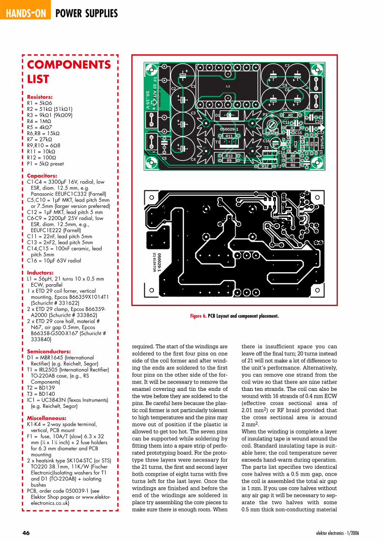
Just one ICThe input voltage in the range from 10to 15 V is connected to terminals K1and K2 in the circuit diagram (Figure4). A PCB mounted fuse is fitted in linewith the positive supply and the spec-ified fuse holder is equipped with twosolder tags for each of the two fusecontact clips, these help to reduce theresistance of the fuse assembly whichis particularly important because itpasses a high current. Four electrolyticcapacitors (C1 to C4) buffer the inputvoltage. The adapter circuit switchesthe supply current very quickly andrequires special low-loss capacitorssuitable for use in switched modepower supplies, the internal imped-ance of normal electrolytics is too high,they would overheat and may burst.C5 decouples any high frequency sig-nals on the supply voltage.The coil (L1) is made up from severallengths of enamel covered wire con-nected in parallel to reduce the skineffect which becomes a problem withhigh switching speed. The high powerswitching element is a HEXFET madeby International Rectifier. This devicehas source/drain resistance of just8 mΩ when it is conducting. The lowresistance ensures very low power dis-sipation in the device and allows it toswitch a hefty 104 A maximum whichshould ensure reliable operation in ourapplication. Both the HEXFET anddiode are fitted with finned heat sinks.Schottky diode D1 has a TO 220 pack-age outline. It has a 45 V maximumoperating voltage and a current of 16 Awhich gives a forward voltage drop ofaround 0.63 V, again for reliability thedevice is conservatively rated. LowESR type electrolytic capacitors arespecified again for output smoothingcapacitors C6 to C9. Capacitor C10 isused for high frequency decouplingand the regulated 19 V is output fromconnectors K3 and K4.A block diagram of the UC3843 (IC1) isshown in Figure 5. It contains a pulsewidth modulated (PWM) controller out-put signal and an internal voltage refer-ence. The adapter output voltage isdivided down by R1, R2, R3 and P1 andconnected to the voltage feedbackinput (pin 2) of the controller IC (theerror amplifier inverting input). C2improves the amplifier stability as doesR4, R5 and C12 connected between
elektor electronics - 1/200644
HANDS-ON POWER SUPPLIES
VOUT[V]
tON [µs]
60
50
40
30
20
125 10 15 20
050029 - 13
VOUT = VIN •tON + tOFF
tOFF
VOUT = 12VtON + tOFF = 25 µs
t
a
t
050029 - 14
b
t
I IN
UT
ILID
∆ IL
VIN
VOUT
IOUTc
t
d
tON tOFF tON
Figure 2. Output voltage control using PWM.
Figure 3. Current and voltage waveforms with 50% on/off switching. (a) The PWM signal; (b) Voltage acrossthe MOSFET (VT); (c) Current through the coil (IL); (d) Current through the diode (ID).
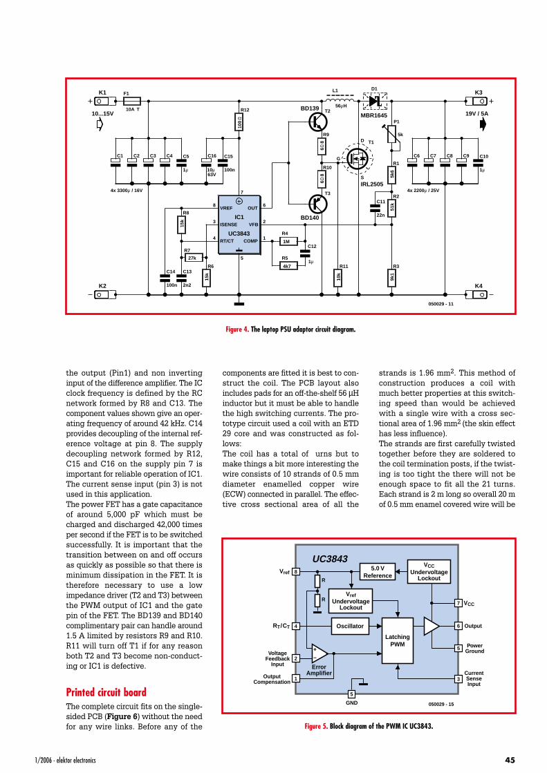
the output (Pin1) and non invertinginput of the difference amplifier. The ICclock frequency is defined by the RCnetwork formed by R8 and C13. Thecomponent values shown give an oper-ating frequency of around 42 kHz. C14provides decoupling of the internal ref-erence voltage at pin 8. The supplydecoupling network formed by R12,C15 and C16 on the supply pin 7 isimportant for reliable operation of IC1.The current sense input (pin 3) is notused in this application.The power FET has a gate capacitanceof around 5,000 pF which must becharged and discharged 42,000 timesper second if the FET is to be switchedsuccessfully. It is important that thetransition between on and off occursas quickly as possible so that there isminimum dissipation in the FET. It istherefore necessary to use a lowimpedance driver (T2 and T3) betweenthe PWM output of IC1 and the gatepin of the FET. The BD139 and BD140complimentary pair can handle around1.5 A limited by resistors R9 and R10.R11 will turn off T1 if for any reasonboth T2 and T3 become non-conduct-ing or IC1 is defective.
Printed circuit boardThe complete circuit fits on the single-sided PCB (Figure 6) without the needfor any wire links. Before any of the
components are fitted it is best to con-struct the coil. The PCB layout alsoincludes pads for an off-the-shelf 56 µHinductor but it must be able to handlethe high switching currents. The pro-totype circuit used a coil with an ETD29 core and was constructed as fol-lows:The coil has a total of urns but tomake things a bit more interesting thewire consists of 10 strands of 0.5 mmdiameter enamelled copper wire(ECW) connected in parallel. The effec-tive cross sectional area of all the
strands is 1.96 mm2. This method ofconstruction produces a coil withmuch better properties at this switch-ing speed than would be achievedwith a single wire with a cross sec-tional area of 1.96 mm2 (the skin effecthas less influence).The strands are first carefully twistedtogether before they are soldered tothe coil termination posts, if the twist-ing is too tight the there will not beenough space to fit all the 21 turns.Each strand is 2 m long so overall 20 mof 0.5 mm enamel covered wire will be
1/2006 - elektor electronics 45
R8
15k
R6
15k
R12
100
Ω
R1
5k6
R2
51k
R3
9k1
R11
10k
R9
6Ω
8
R10
6Ω
8
C13
2n2
C14
100n
C15
100n
C5
1µ
C10
1µ
C11
22n
IRL2505
T1
S
D
G
R7
27k
UC3843
ISENSE
RT/CT
IC1
COMP
VREF OUT
VFB
6
7
5
1
2
8
4
3
R4
1M
R5
4k7
C12
1µ
5k
P1
T2BD139
T3
BD140
D1
MBR1645
C16
10µ63V
C1 C2 C3 C4 C6 C7 C8 C9
L1
56µH
K3
K4
K1
K2
10A T
F1
10...15V 19V / 5A
050029 - 11
4x 3300µ / 16V 4x 2200µ / 25V
VrefUndervoltage
Lockout
LatchingPWM
5.0 VReference
Oscillator
ErrorAmplifier
VCCUndervoltage
Lockout8
R
R
Vref
4RT/CT
2Voltage
FeedbackInput
1OutputCompensation
5
GND
7 VCC
6 Output
5 PowerGround
3
050029 - 15
CurrentSenseInput
UC3843
Figure 4. The laptop PSU adaptor circuit diagram.
Figure 5. Block diagram of the PWM IC UC3843.
required. The start of the windings aresoldered to the first four pins on oneside of the coil former and after wind-ing the ends are soldered to the firstfour pins on the other side of the for-mer. It will be necessary to remove theenamel covering and tin the ends ofthe wire before they are soldered to thepins. Be careful here because the plas-tic coil former is not particularly tolerantto high temperatures and the pins maymove out of position if the plastic isallowed to get too hot. The seven pinscan be supported while soldering byfitting them into a spare strip of perfo-rated prototyping board. For the proto-type three layers were necessary forthe 21 turns, the first and second layerboth comprise of eight turns with fiveturns left for the last layer. Once thewindings are finished and before theend of the windings are soldered inplace try assembling the core pieces tomake sure there is enough room. When
there is insufficient space you canleave off the final turn; 20 turns insteadof 21 will not make a lot of difference tothe unit’s performance. Alternatively,you can remove one strand from thecoil wire so that there are nine ratherthan ten strands. The coil can also bewound with 16 strands of 0.4 mm ECW(effective cross sectional area of2.01 mm2) or RF braid provided thatthe cross sectional area is around2 mm2.When the winding is complete a layerof insulating tape is wound around thecoil. Standard insulating tape is suit-able here; the coil temperature neverexceeds hand-warm during operation.The parts list specifies two identicalcore halves with a 0.5 mm gap, oncethe coil is assembled the total air gapis 1 mm. If you use core halves withoutany air gap it will be necessary to sep-arate the two halves with some0.5 mm thick non-conducting material
elektor electronics - 1/200646
HANDS-ON POWER SUPPLIES
(C) ELEKTOR
050029-1
C1C2
C3
C4C5
C6
C7
C8
C9
C10C11
C12
C13C14
C15
C16
D1
F1
IC1
L1
P1 R1
R2
R3
R4
R5
R6R7R8
R9R10
R11
R12
T1
T2
T3
+
19V
/5A
-
+
10 A
/T
-
10..1
5 V
050029-1
(C) E
LEK
TOR
05
00
29
-1
Figure 6. PCB Layout and component placement.
COMPONENTSLISTResistors:R1 = 5kΩ6R2 = 51kΩ (51kΩ1)R3 = 9kΩ1 (9kΩ09)R4 = 1MΩR5 = 4kΩ7R6,R8 = 15kΩR7 = 27kΩR9,R10 = 6Ω8R11 = 10kΩR12 = 100ΩP1 = 5kΩ preset
Capacitors:C1-C4 = 3300µF 16V, radial, low
ESR, diam. 12.5 mm, e.g.Panasonic EEUFC1C332 (Farnell)
C5,C10 = 1µF MKT, lead pitch 5mmor 7.5mm (larger version preferred)
C12 = 1µF MKT, lead pitch 5 mmC6-C9 = 2200µF 25V radial, low
ESR, diam. 12.5mm, e.g.,EEUFC1E222 (Farnell)
C11 = 22nF, lead pitch 5mmC13 = 2nF2, lead pitch 5mmC14,C15 = 100nF ceramic, lead
pitch 5mmC16 = 10µF 63V radial
Inductors:L1 = 56µH, 21 turns 10 x 0.5 mm
ECW, parallel1 x ETD 29 coil forner, vertical
mounting, Epcos B66359X1014T1(Schuricht # 331622)
2 x ETD 29 clamp, Epcos B66359-A2000 (Schuricht # 333862)
2 x ETD 29 core half, material #N67, air gap 0.5mm, EpcosB66358-G500-X167 (Schuricht #333840)
Semiconductors:D1 = MBR1645 (International
Rectifier) (e.g. Reichelt, Segor)T1 = IRL2505 (International Rectifier)
TO-220AB case, (e.g., RSComponents)
T2 = BD139T3 = BD140IC1 = UC3843N (Texas Instruments)
(e.g. Reichelt, Segor)
Miscellaneous:K1-K4 = 2-way spade terminal,
vertical, PCB mountF1 = fuse, 10A/T (slow) 6.3 x 32
mm (1⁄4 x 11⁄4 inch) + 2 fuse holdersfor 6.3 mm diameter and PCBmounting
2 x heatsink type SK104-STC (or STS)TO220 38.1mm, 11K/W (FischerElectronic)Isolating washers for T1and D1 (TO-220AB) + isolatingbushes
PCB, order code 050039-1 (seeElektor Shop pages or www.elektor-electronics.co.uk)

in order to achieve the 1 mm air gap.Larger outline capacitors were chosenfor C5 and C10 with a lead spacing of7.5 mm, these are better at handlinghigh current and have lower losses.Begin assembly by fitting the resistorsto the PCB then the fuse holder, nextcomes the spade connectors then the
preset followed by the electrolyticcapacitors (observe correct polarity)and the coil assembly.Before the FET and diode are solderedinto the PCB a bend should be intro-duced in the leads to help reduce themechanical stresses on the solderedjoints when the device heats up. Both
semiconductors must be insulated fromtheir heat sink using insulating wash-ers and an insulated bush for the M3mounting bolts and don’t forget toapply a little thermal compound.Ensure that these devices are well sol-dered in place because the leads willbe carrying several amps. The heatsink
1/2006 - elektor electronics 47
Figure 7. All components including the wound coil fitted to the prototype board.
Test results and efficiencyInput voltage
(V)Input current
(A)Input power
(W)Output voltage
(V)Output current
(A)Output power
(W)Efficiency η
(%)10.8 4.25 45.9 18.93 2.32 43.9 95.710.8 5.59 60.4 18.92 3.05 57.7 95.610.8 8.49 91.7 18.90 4.59 86.8 94.610.8 11.23 121.3 18.88 5.99 113.1 93.212.0 3.84 46.1 18.93 2.34 44.3 96.112.0 5.06 60.7 18.92 3.08 58.3 96.012.0 7.63 91.6 18.90 4.62 87.3 95.412.0 10.00 120.0 18.89 6.00 113.3 94.513.2 3.48 45.9 18.94 2.33 44.1 96.113.2 4.56 60.2 18.93 3.06 57.9 96.213.2 6.91 91.2 18.91 4.61 87.2 95.613.2 9.03 119.2 18.89 5.99 113.2 94.914.4 3.18 45.8 18.95 2.33 44.2 96.414.4 4.16 59.9 18.94 3.05 57.8 96.414.4 6.29 90.6 18.92 4.61 87.2 96.314.4 8.24 118.7 18.90 6.00 114.4 95.6

can be taller, i.e., 50.8 or 63.5 mm with9 K/W or 8 K/W respectively. The proto-type is fitted with 38.1 mm high heatsink at 11 K/W. From the efficiencyviewpoint it would be better if thediode had a smaller heat sink becausethe diode’s forward conduction voltagedecreases with increasing temperature.However a smaller heat sink may leadto overheating if the output is over-loaded. A 20TQ045 diode from IRF canbe substituted for D1; this device has aslightly smaller forward voltage drop.There is no advantage in letting theFET run warmer, its channel resistance(RDSon) increases with increasing tem-perature. Finally fit transistors T2 andT3 along with IC1 and take the oppor-tunity to double check all the compo-nents and soldering before you moveon to the next phase and connectpower to the adapter.
Power onBefore the unit is powered up for thefirst time turn the preset P1 fully clock-wise to produce the minimum output
voltage. For testing use either a powersupply capable of supplying 12 V at10 A or a 12 V vehicle battery. Initiallyadjust the power supply current limitto 200 mA or, if you are using a battery,connect a 5 W resistor (47 or 56 Ω) inseries with the positive supply lead tothe adapter. Double check that the pos-itive lead of the power supply is con-nected to K1 and the negative lead toK2 (nearest to the PCB corner). Whenno obvious malfunction occurs with thepower connected (no excess currentdrawn from the supply and no smokesignals…) the current limit can beincreased (or the series resistorremoved). Connect a multimeter to theadapter output connections K3 and K4(the negative terminal is nearest theboard corner again) and check that theoutput voltage lies in the range of 18 to19 V. With no load connected to theadapter slowly adjust P1 to ensure thatit can achieve an output voltage of19.4 V. Now use either an electronicload or a combination of high powerresistors (4.8 Ω at 100 W) and adjust P1for 19 V output voltage at full load (5 A).
You may notice that when the adapter isoperating under full load conditions theoutput voltage will bounce up brieflyby 1 V whenever the load is discon-nected. The output quickly returns toits regulated level and in practice thisdesign ‘feature’ is not a problem for alaptop adapter application.The finished unit can be mounted inan enclosure. The high efficiencyachieved by this design means thatvery little heat is produced by the unitand there is no need for a fan. A fewholes in the case will be sufficient justto allow a little air circulation. Beforethe unit is connected to the cigarettelighter socket make sure that it (andthe plug) are capable of handling 10 A.Connect the adapter to the PC with asuitable lead and connector, doublecheck that the plus and minus are con-nected to the correct input pin of thelaptop or notebook PC — neverassume that it is equipped withreverse voltage protection!
(050029-1)
Michael Schö[email protected]
elektor electronics - 1/200648
HANDS-ON POWER SUPPLIES
Advertisement