Embed Size (px)
Citation preview
UNIVERSITY OF PADOVA
FACULTY OF ENGINEERING
DEPARTMENT OF INFORMATION ENGINEERING
MASTER OF SCIENCE IN ELECTRONIC ENGINEERING
MASTER'S THESIS
94 GHz Monolithic Transmitter forWeather Radar Application
UNIVERSITY SUPERVISOR:Prof. Andrea Neviani
COMPANY SUPERVISOR:Ph.D. Marc Tiebout
GRADUAND:Claudio Puliero
ACADEMIC YEAR 2010/2011

94 GHz Monolithic Transmitter for Weather Radar Application
Abstract
This thesis was written for concluding my studies at the University of Padua. The
main topic is the design of a monolithic transmitter in SiGe bipolar technology, for
weather radar application at an operating frequency around 94GHz. At such a high
frequency parasitic elements have to be taken into account very carefully.
Appropriate matching networks become important to allow the signals to pass
across the different sections of the transmitter, without reflections or attenuations.
To this aim, transmission lines were used instead of inductors, in order to save size
and to have a more reliable modelling of device parameters and parasitic elements.
The structure of the transmitter includes a transformer (which acts as Balun), a
frequency quadrupler and a buffer. The transmitter input receives a single-ended
reference signal at 23.5GHz, with a power of 0dBm on a single-ended input
impedance of 50Ω. The output has been designed for a differential load of 100Ω
and to operate in the temperature range of 0°C - 100°C, with a typical output
power above 10dBm and spurious harmonic below -25dBc.
i

94 GHz Monolithic Transmitter for Weather Radar Application
Acknowledgment
First of all, I would like to thank Infineon Austria (site of Villach), the Industrial &
Multimarket (IMM) and the RF power groups, which gave me the opportunity to
make my thesis through an internship into their company. I'm very grateful to Marc
Tiebout for his availability, his teachings and his big patience during my questions
and my errors. A thanks also to all the colleague that I met during this experience
into Infineon, whom helped me to spend seven pleasant months in Austria and that
aided me during the hard times.
A special thanks to my high school (ITIS Severi), which has let me discover the
electronic, in particular to Prof. Daniele Consolaro who encouraged me to inscribe at
the university.
A great thanks to the University of Padua which formed and trained me on the way
of electronic engineer. My sincere gratitude to all the group of IC design at my
university and to Professor Andrea Neviani who sponsored my thesis in Infineon
Austria and also helped me to draft it.
Most of all, I must to acknowledge my parents and my sister, that supported me
during all my student's career, helping me during the worst of times and rejoicing
with me over the best one. Thanks very much to my parents for have grown me up
and for have paid my studies.
Last but not least a great thanks to all my friends, starting from my childhood
friends up to the last Austrians ones, through my basket team and my LAN party
crew. A fervent thought at that mates who chose a different way and now live far
from me, I wish you a wonderful life!!
A last thanks to all people that I have forgotten, but who had a significant role into
my academic studies and also in my life.
ii
94 GHz Monolithic Transmitter for Weather Radar Application
Table of Contents
AbstractAcknowledgmentTable of contents
1. Introduction _____________________________________________ 11.1. Weather Radars system .................................................................. 2
1.1.1. Clouds studies ........................................................................ 51.1.2. Brief story of weather radars .................................................... 61.1.3. Weather radar functioning ....................................................... 8
1.2. Other transmitter bandwidth possible applications ............................ 101.3. Transmitter overview .................................................................... 11
1.3.1. Target structure diagram ....................................................... 131.3.2. Target specifications .............................................................. 141.3.3. Transmitter for imaging in body scanner .................................. 17
2. Technology overview _____________________________________ 192.1. Infineon's B7HF200 ...................................................................... 212.2. Bipolar characteristics .................................................................. 242.3. Chip packaging and measure problems ........................................... 272.4. Use of transmission lines .............................................................. 28
3. Input network __________________________________________ 313.1. Bonding and pads ........................................................................ 313.2. Transformer ................................................................................ 33
3.2.1. Choice of transformer ............................................................ 333.2.2. Lumped model fitting ............................................................ 35
4. Quadrupler _____________________________________________ 374.1. Circuit operation .......................................................................... 38
4.1.1. Gilbert cell as frequency doubler ............................................. 394.1.2. Bias circuit ........................................................................... 42
4.2. Design to 94GHz .......................................................................... 444.2.1. Gain stage ........................................................................... 454.2.2. Interstage matching and quadrature phase .............................. 474.2.3. Matching networks ................................................................ 504.2.4. Stability .............................................................................. 524.2.5. Design result ........................................................................ 54
iii
94 GHz Monolithic Transmitter for Weather Radar Application
4.3. Layout ........................................................................................ 554.3.1. Post-layout issues ................................................................. 56
4.4. Final circuit and simulation results .................................................. 57
5. Buffer _________________________________________________ 635.1. Circuit operation .......................................................................... 64
5.1.1. Cascode configuration ........................................................... 655.1.2. Bias circuit ........................................................................... 66
5.2. Design to 94GHz .......................................................................... 675.2.1. Gain stage ........................................................................... 685.2.2. Interstage matching .............................................................. 705.2.3. Matching networks ................................................................ 705.2.4. Stability .............................................................................. 735.2.5. Design result ........................................................................ 74
5.3. Layout ........................................................................................ 745.3.1. Post-layout issues ................................................................. 75
5.4. Final circuit and simulation results .................................................. 76
6. Power amplifier _________________________________________ 816.1. Possible configurations and functioning ........................................... 816.2. Emitter follower plus cascode ........................................................ 83
6.2.1. Design ................................................................................ 856.2.2. Simulation results ................................................................. 85
6.3. Cascode ..................................................................................... 866.3.1. Design ................................................................................ 876.3.2. Simulation results ................................................................. 886.3.3. Low output power due to layout parasitic elements .................... 89
6.4. Removal of power amplifier ........................................................... 89
7. Top level circuit _________________________________________ 917.1. Schematic ................................................................................... 917.2. Layout ........................................................................................ 937.3. Simulations results ...................................................................... 94
8. Conclusions ___________________________________________ 100
Bibliography
iv
Chapter 1: Introduction
Chapter 1: Introduction
The main goal of RADARs is to scan the open space, or an object, and then
reconstruct its image through the electromagnetic energy reflected back, from the
object to the radar station. The optical image is created by mapping the
electromagnetic scattering coefficient onto a two-dimensional plane. Objects with a
higher coefficient are assigned to a higher optical reflective index.
Transmitter structure is basically the same for most of the RADARs; the main
parameter is the frequency, which depends on the field of use. To choose the right
operative frequency for the RADAR, it depends principally on the dimension of the
object that have to be scanned. An increase of the operating frequency means to be
able to recognize smaller objects and to have a higher resolution. It is also helpful
for decreasing the dimension of the RADAR antenna, which enables to put these
devices into portable or mobile structures like cars or planes. On the other hand at
higher frequency we have much more construction costs for the transmitter and in
the most case also more power consumption and lower efficiency.
With a lower size of the transmitter it is also possible to construct phased array
antennas, which are more performant. They are also more reliable because they
are without the mechanical structure, which moves the antenna into the right
direction for scanning all the space. In these kind of antennas, the relative phases
of the respective signals feeding the antennas, are varied in such a way that the
effective radiation pattern, of the array, is reinforced in a desired direction and
suppressed in undesired directions.
1
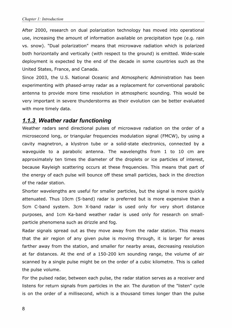
Figure 1.1: Atmospheric opacity vs. wavelength
Chapter 1: Introduction
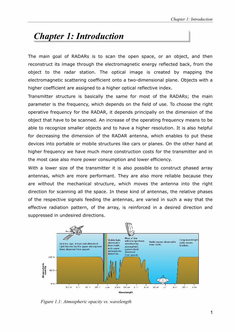
Another issue to take into account for long distance and high frequency RADAR
application (into the free-space), is the absorption of electromagnetic radiation due
to the Earth's atmosphere. The combined absorption spectra of the gases in the
atmosphere leave "windows" of low opacity, allowing the transmission only into
certain frequency bands. One of these small windows is also present around the
94GHz working frequency of this transmitter, which is one of the reasons why this
frequency has been chosen.
Also the free-space path loss has to be considered. It is proportional to the square
of the distance between the transmitter and receiver, and also proportional to the
square of the frequency of the radio signal. Higher frequency means higher
attenuation for the same distance.
From these considerations weather radars will be the main target for the 94GHz
monolithic transmitter design treated in these pages. Despite that some other
possible applications could be found and they will be shown in a following section.
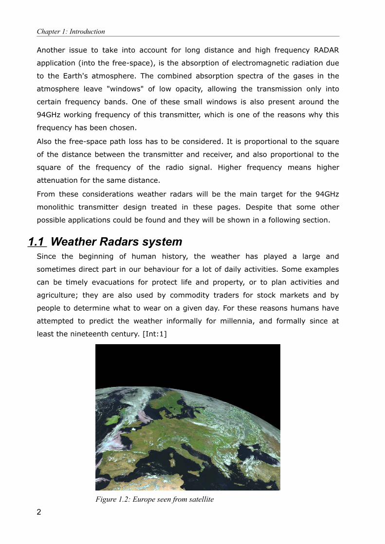
1.1 Weather Radars systemSince the beginning of human history, the weather has played a large and
sometimes direct part in our behaviour for a lot of daily activities. Some examples
can be timely evacuations for protect life and property, or to plan activities and
agriculture; they are also used by commodity traders for stock markets and by
people to determine what to wear on a given day. For these reasons humans have
attempted to predict the weather informally for millennia, and formally since at
least the nineteenth century. [Int:1]
2Figure 1.2: Europe seen from satellite
Chapter 1: Introduction
The weather forecasts are made by collecting quantitative data about the current
state of the atmosphere and using scientific understanding of atmospheric
processes to project how the atmosphere will evolve. The basic idea of numerical
weather prediction is to sample the state of the fluid at a given time and use the
equations of fluid dynamics and thermodynamics to estimate the state of the fluid
at some time in the future.
The main inputs from country-based weather services are surface observations,
from automated weather stations at ground level, over land, and from weather
buoys at sea. The World Meteorological Organization acts to standardize the
instrumentation, observing practices and timing of these observations worldwide.
Stations either report hourly in METAR reports or every six hours in SYNOP reports.
Sites launch radiosondes, which rise through the depth of the troposphere and well
into the stratosphere. Data from weather satellites are used in areas of where
traditional data sources are not available. Compared with similar data from
radiosondes, the satellite data has the advantage of global coverage, however at a
lower accuracy and resolution.
Some commercial planes provide reports along their aircraft routes and also the
ships report information along their shipping route. Research flights using
reconnaissance aircraft fly in and around weather systems of interest such as
tropical cyclones. Reconnaissance aircraft are also flown over the open oceans
during the cold season into systems which cause significant uncertainty in forecast
guidance, or are expected to be of high impact 3-7 days into the future over the
downstream continent.
Weather radar systems (typically Arinc 708 on commercial aircraft) and lightning
detectors, are important also for aircraft flying at night, or in instrument
meteorological conditions, where it is not possible for pilots to see the weather
ahead. Theirs main goal is to improve the daily weather report and to make flying
safer by providing pilots with real-time heavy precipitation, icing conditions (sensed
by radar) or turbulence (sensed by lightning activity). These are both indications of
strong convective activity and severe turbulence, weather systems allow pilots to
deviate around these dangerous areas.
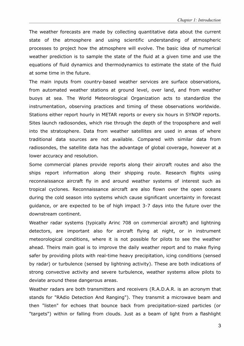
Weather radars are both transmitters and receivers (R.A.D.A.R. is an acronym that
stands for "RAdio Detection And Ranging"). They transmit a microwave beam and
then "listen" for echoes that bounce back from precipitation-sized particles (or
"targets") within or falling from clouds. Just as a beam of light from a flashlight
3
Chapter 1: Introduction
shows objects in the dark, weather radar detects and locates precipitation, but it
does so both in daylight and darkness, through thick clouds, and at greater
distances than can a flashlight beam. Both the flashlight and weather radar work on
the same principle: a small part of the transmitted energy is reflected back towards
the source after striking an object.
Into each weather station there is a meteorological radar, which provides
information on precipitation location and intensity, that can be used to estimate
precipitation accumulations over time. So weather radar are a versatile tool for
atmospheric assessment, with uses that include:
• Rainfall estimates
• Real-time cloud detection
• Speed and direction of cell motion
• Identifying precipitation location and intensity
In addition modern weather radars are mostly pulse-Doppler radars, which are
capable of measuring if whether precipitation echoes are moving toward or away
from the radar antenna, and can therefore measure rotation within storms which
may precede severe storms. Generally a “Pulse Doppler” weather radar is also used
to determine the wind speed and direction.
Meteorologists use weather radar to detect, locate, and measure the amount of
precipitation within or falling from clouds. From weather forecast studies derive the
importance of a good weather radars, with a high resolution, that means high
operative frequency. This is the reason why it will be presented a suggestion of a
monolithic transmitter cell at 94 GHz, for potential weather uses.
4
Figure 1.3: Typical weather antennas

Chapter 1: Introduction
1.1.1 Clouds studiesA cloud is a visible mass of water droplets or frozen ice crystals suspended in the
Earth's atmosphere above the surface of the Earth or other planetary body. Two
processes, possibly acting together, can lead to air becoming saturated: cooling the
air or adding water vapour to the air. Generally, precipitation will fall to the surface;
an exception is virga which evaporates before reaching the surface. [Int:1]
Clouds can show convective development like cumulus, be in the form layered
sheets such as stratus, or appear in thin fibrous wisps as with cirrus. Whether or
not a cloud is low, middle, or high level depends on how far above the ground its
base forms. Some cloud types can form in the low or middle ranges depending on
the moisture content of the air. While a majority of clouds form in the Earth's
troposphere, there are occasions where clouds in the stratosphere and mesosphere
are observed. All weather-related cloud types form in the troposphere, the lowest
major layer of the Earth's atmosphere. Clouds have been observed on other planets
and moons within the Solar System, but due to their different temperature
characteristics, they are composed of other substances such as methane, ammonia,
or sulphuric acid.
Clouds are a key element in the global hydrological cycle, and they have a
significant role in the Earth’s energy budget through its influence on radiation
budgets. Climate model simulations have demonstrated the importance of clouds in
moderating and forcing the global energy. An improved understanding of the
5
Figure 1.4: Clouds types
Chapter 1: Introduction
radioactive impact of clouds on the climate system requires a comprehensive view
of clouds that includes their physical dimensions, vertical and horizontal spatial
distribution, detailed micro-physical properties, and the dynamical processes
producing them.
For this purpose millimetre-wave cloud radars at W-band were designed. They are
radar system designed to monitor cloud structure with a wavelengths about ten
times shorter than those used in conventional storm surveillance radars such as
NEXRAD. These radars provide fine scale cloud information and offer significant
advantages over LIDAR and lower frequency radars. The high scattering efficiency
and short wavelengths at millimetre-wave frequencies provide high sensitivity for
cloud detection, and enable construction of compact, low-power consumption
radars for use in airborne applications.
The National Oceanic and Atmospheric Administration designed MMCR to monitor
clouds overhead at various testing sites of the U.S. Department of Energy's
atmospheric radiation measurement program. The MMCR is a vertically pointing
Doppler weather radar that operates at a frequency of 35GHz. The main purpose of
this radar is to determine cloud boundaries (e.g., cloud bottoms and tops). The
shorter wavelength of the radar helps detect tiny water and ice droplets that
conventional radars are unable to "see". The radar also helps to estimate
microphysical properties of clouds, such as particle size and mass content, which
aids in understanding how clouds reflect, absorb and transform radiant energy
passing though the atmosphere. MMCR also reports radar reflectivity (dBZ) of the
atmosphere up to 20km and possesses the capability to measure vertical velocities
of cloud constituents.
1.1.2 Brief story of weather radarsDuring World War II, military radar operators noticed noise in returned echoes due
to weather elements like rain, snow, and sleet. [Int:1] Just after the war, military
scientists returned to civilian life or continued in the Armed Forces and pursued
their work in developing a use for those echoes. In the United States, David Atlas
developed the first operational weather radars. In Canada, J.S. Marshall and R.H.
Douglas formed the "Stormy Weather Group" in Montreal. Marshall and his doctoral
student Walter Palmer are well known for their work on the drop size distribution in
mid-latitude rain that led to understanding of the Z-R relation, which correlates a
given radar reflectivity with the rate at which water is falling on the ground. In the
6

Chapter 1: Introduction
United Kingdom, research continued to study the radar echo patterns and weather
elements such as stratiform rain and convective clouds, and experiments were done
to evaluate the potential of different wavelengths from 1 to 10 centimetres.
In 1953, Donald Staggs, an electrical engineer working for the Illinois State Water
Survey, made the first recorded radar observation of a "hook echo" associated with
a tornadic thunderstorm.
Between 1950 and 1980, reflectivity radars, which measure position and intensity
of precipitation, were built by weather services around the world. The early
meteorologists had to watch a cathode ray tube. During the 1970s, radars began to
be standardized and organized into networks. The first devices to capture radar
images were developed. The number of scanned angles was increased to get a
three-dimensional view of the precipitation, so that horizontal cross-sections
(CAPPI) and vertical ones could be performed
The National Severe Storms Laboratory, created in 1964, began experimentation on
dual polarization signals and on Doppler effect uses. In May 1973, a tornado
devastated Union City, Oklahoma, just west of Oklahoma City. For the first time, a
Dopplerized 10cm wavelength radar from NSSL documented the entire life cycle of
the tornado. The researchers discovered a mesoscale rotation in the cloud aloft
before the tornado touched the ground: the tornadic vortex signature. NSSL's
research helped convince the National Weather Service that Doppler radar was a
crucial forecasting tool.
Between 1980 and 2000, weather radar networks became the norm in North
America, Europe, Japan and other developed countries. Conventional radars were
replaced by Doppler radars, which in addition to position and intensity of could
track the relative velocity of the particles in the air. In the United States, the
construction of a network consisting of 10cm wavelength radars, called NEXRAD or
WSR-88D (Weather Service Radar 1988 Doppler), was started in 1988 following
NSSL's research. In Canada, Environment Canada constructed the King City station,
with a five centimetre research Doppler radar, by 1985; McGill University
dopplerized its radar (J. S. Marshall Radar Observatory) in 1993. This led to a
complete Canadian Doppler network between 1998 and 2004. France and other
European countries switched to Doppler network by the end of the 1990s to early
2000s. Meanwhile, rapid advances in computer technology led to algorithms to
detect signs of severe weather and a plethora of "products" for media outlets and
researchers.
7
Chapter 1: Introduction
After 2000, research on dual polarization technology has moved into operational
use, increasing the amount of information available on precipitation type (e.g. rain
vs. snow). "Dual polarization" means that microwave radiation which is polarized
both horizontally and vertically (with respect to the ground) is emitted. Wide-scale
deployment is expected by the end of the decade in some countries such as the
United States, France, and Canada.
Since 2003, the U.S. National Oceanic and Atmospheric Administration has been
experimenting with phased-array radar as a replacement for conventional parabolic
antenna to provide more time resolution in atmospheric sounding. This would be
very important in severe thunderstorms as their evolution can be better evaluated
with more timely data.
1.1.3 Weather radar functioningWeather radars send directional pulses of microwave radiation on the order of a
microsecond long, or triangular frequencies modulation signal (FMCW), by using a
cavity magnetron, a klystron tube or a solid-state electronics, connected by a
waveguide to a parabolic antenna. The wavelengths from 1 to 10 cm are
approximately ten times the diameter of the droplets or ice particles of interest,
because Rayleigh scattering occurs at these frequencies. This means that part of
the energy of each pulse will bounce off these small particles, back in the direction
of the radar station.
Shorter wavelengths are useful for smaller particles, but the signal is more quickly
attenuated. Thus 10cm (S-band) radar is preferred but is more expensive than a
5cm C-band system. 3cm X-band radar is used only for very short distance
purposes, and 1cm Ka-band weather radar is used only for research on small-
particle phenomena such as drizzle and fog.
Radar signals spread out as they move away from the radar station. This means
that the air region of any given pulse is moving through, it is larger for areas
farther away from the station, and smaller for nearby areas, decreasing resolution
at far distances. At the end of a 150-200 km sounding range, the volume of air
scanned by a single pulse might be on the order of a cubic kilometre. This is called
the pulse volume.
For the pulsed radar, between each pulse, the radar station serves as a receiver and
listens for return signals from particles in the air. The duration of the "listen" cycle
is on the order of a millisecond, which is a thousand times longer than the pulse
8
Chapter 1: Introduction
duration. The length of this phase is determined by the need for the microwave
radiation (which travels at the speed of light) to propagate from the detector, to the
weather target, and back again, for distances which could be several hundred
kilometres.
The horizontal distance from station to target is calculated simply from the amount
of time that lapses from the initiation of the pulse to the detection of the return
signal. (The time is converted into distance by multiplying by the speed of light). If
pulses are emitted too frequently, the returns from one pulse will be confused with
the returns from previous pulses, resulting in incorrect distance calculations. In
order to determine the height we can assume that the Earth is round. With
knowledge of the variation of the index of refraction through air and the distance to
the target, it can be calculated the height above ground of the target.
FMCW radars, instead, are systems where a known stable frequency continuous
wave radio energy is modulated by a triangular modulation signal, so that it varies
gradually. This transmit signal is then mixed with the reflected from a target object
to produce the information signal. The received waveform is almost a delayed
replica of the transmitted waveform and the time delay is a measure of the
distance.
Each weather radar network uses a series of typical angles that will be set
according to the needs. After each scanning rotation, the antenna elevation is
changed for the next sounding. This scenario will be repeated on many angles to
scan all the volume of air around the radar within the maximum range. Usually, this
scanning strategy is completed within 5 to 10 minutes to have data within 15km
above ground and 250km distance of the radar.
Due to the Earth curvature and change of index of refraction with height, the radar
cannot "see" below the height above ground of the minimal angle or closer to the
radar than the maximal one.
Doppler weather radar has become increasingly popular in recent years. It is
capable of measuring the approach (or departing) speed of raindrops. The Doppler
principle can be explained by noting the change in pitch of an ambulance siren. The
pitch heightens as the ambulance approaches and lowers as it departs. In other
words, the faster the ambulance approaches, the higher will be the pitch. For the
case of a Doppler radar, the faster the raindrops move towards the radar, the higher
will be the frequency (i.e. pitch) of the microwave reflected from raindrops. The
9

Chapter 1: Introduction
raindrops approach speed is determined by the frequency shift, and provides a
good estimation of the winds, which carry the raindrops.
1.2 Other transmitter bandwidth possible applicationsSome other 94GHz transmitter possible applications were studied during last years,
they could be found on internet, but most of them are for military use and poor
information are shown. [Appleby:04] [Int:1]
One example is a real-time 94GHz passive millimetre-wave imager for helicopter
operations, that can penetrate poor weather far better than infrared or visible
systems. Imaging in this band offers the opportunity for passive surveillance and
navigation allowing military operations in poor weather. This 94GHz imager has
diffraction limited performance over the central two thirds of the 30 x 60 degrees
field of view with and a 25Hz frame update rate.
Another military use is the Active Denial System (ADS) that is a non-lethal,
directed-energy weapon developed by the U.S. military. It is a strong millimetre-
wave transmitter primarily used for crowd control (the "goodbye effect"). Some
ADS such as HPEM ADS are also used to disable vehicles. Informally, the weapon is
also called heat ray.
The ADS works by firing a high-powered beam of electromagnetic radiation in the
form of high-frequency millimetre waves at 95 GHz (a wavelength of 3.2 mm).
Similar to the same way that a microwave oven heats food, the millimetre waves
excite the water and fat molecules in the body, instantly heating it and causing
10
Figure 1.5: Doppler weather RADAR
Chapter 1: Introduction
intense pain. Note that while microwaves will penetrate human tissue and remove
the water to "cook" the flesh, the millimetre waves used in ADS are blocked by cell
density and only penetrate the top layers of skin, so it will not damage human
flesh.
Such is the nature of dielectric heating that the temperature of a target will
continue to rise so long as the beam is applied, at a rate dictated by the target's
material and distance, along with the beam's frequency and power level set by the
operator. Like all focused energy, the beam will irradiate all matter in the targeted
area, including everything beyond/behind it that is not shielded, with no possible
discrimination between individuals, objects or materials, although highly conductive
materials such as aluminium cooking foil should reflect this radiation and could be
used to make clothing that would be protective against this radiation. All living
things in the target area receive a similar dosage of radiation.
In addition some passive millimetre-wave cameras for concealed weapons detection
operate at 94 GHz. Atmospheric radio window at 94 GHz is used for imaging
millimetre-wave radar applications in astronomy, defence, and security applications.
Also some notes on a 94GHz automobile collision-avoidance radar was found, but in
automotive the typical used frequency is around 77GHz. [Moldovan:04]
The designed transmitter is not suitable for transceiver uses for data signals. As we
will see, this is due to the presence of a fundamental tone frequency doubler, which
produces a considerable intermodulation distortion for signals in a potential data
bandwidth.
1.3 Transmitter overviewIn electronics and telecommunications a transmitter or radio transmitter is an
electronic device which, with the aid of an antenna, produces radio waves. The
transmitter itself generates a radio frequency alternating current (or voltage),
which is applied to the antenna. When excited by this alternating current, the
antenna radiates radio waves.
Depending on the specific application, the peak powers generated by the radar
transmitter can range from milliwatts to gigawatts. Both thermionic tube-type
transmitters and solid-state transmitters are used. If the transmitter is specified to
generate high average power, than typically an amplifier based on vacuum tube
technology will be required. [Book:6]
The transition from high-power klystrons, traveling wave tubes (TWTs), crossed-
11
Chapter 1: Introduction
field amplifiers (CFAs), and magnetrons, to solid-state electronics has actually been
very gradual because the power output of individual solid-state devices is quite
limited compared to typical radar requirements. Nevertheless, transmitter designers
have learned that the required higher power levels, for radar transmitters, can be
achieved also with a solid-state technology, because transistors and transistor
amplifier modules can be readily combined in parallel, to achieve a composite
higher equivalent output power. Anyway both vacuum tubes and solid-state devices
will be appealing in high performance radars for many years to come.
For this project it has been used a solid-state configuration thanks to the availability
of a silicon technology, and also because we point to a target market of planes and
phased-array antennas. In these fields low sizes are required, besides some other
characteristics become relevant, compared to tube-type transmitters, like lower
supply voltages and an higher meantime between failures (MTBF). [Book:5]
Another distinction that can be made for transmitters is between broadcasting
transmitters and RADAR transmitters. Ordinarily the first ones are the most
complicated, because, in order to broadcast information, a modulation process is
needed for the data signal. Recent and most used frequency modulation requires
more exacting specifications for the harmonic distortion and intermodulation in the
data signal bandwidth, and also adequate rejection of noise. For these reasons, in
these cases more complex circuits are implemented.
The transmitters for RADARs, instead, are used for sending a signal with a desired
power at one single frequency or quasi-static frequency modulated signal (in case
of FMCW radar), for then watching which is the reflected power that returns back to
the antenna, or the frequency variation due to Doppler effect. More relaxed circuits
can be used at this purpose.
Generally around the transmitter there are also some other circuits, that all
together form the RADAR system. These are the RF path, the receiver, the signal
processing circuits and the devices that act to control and synchronize all the
functional blocks. Even the transmitter can be divided into some small blocks: the
signal generator (usually a voltage oscillator), the signal modulator (not always
present) and an amplification stage. This is also the structure of our transmitter,
which will be analysed with more detail in the next sections.
12
Chapter 1: Introduction
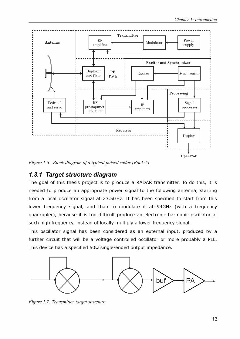
1.3.1 Target structure diagramThe goal of this thesis project is to produce a RADAR transmitter. To do this, it is
needed to produce an appropriate power signal to the following antenna, starting
from a local oscillator signal at 23.5GHz. It has been specified to start from this
lower frequency signal, and than to modulate it at 94GHz (with a frequency
quadrupler), because it is too difficult produce an electronic harmonic oscillator at
such high frequency, instead of locally multiply a lower frequency signal.
This oscillator signal has been considered as an external input, produced by a
further circuit that will be a voltage controlled oscillator or more probably a PLL.
This device has a specified 50Ω single-ended output impedance.
13
Figure 1.6: Block diagram of a typical pulsed radar [Book:5]
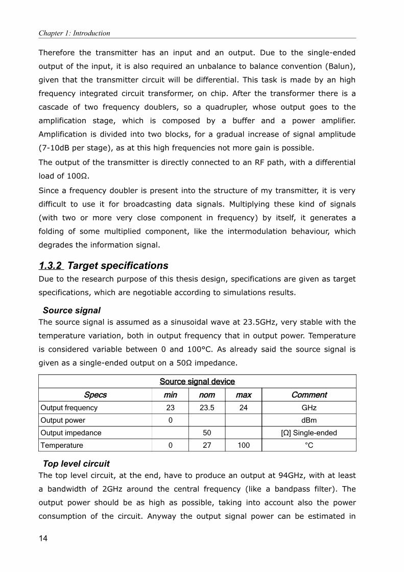
Figure 1.7: Transmitter target structure
Chapter 1: Introduction
Therefore the transmitter has an input and an output. Due to the single-ended
output of the input, it is also required an unbalance to balance convention (Balun),
given that the transmitter circuit will be differential. This task is made by an high
frequency integrated circuit transformer, on chip. After the transformer there is a
cascade of two frequency doublers, so a quadrupler, whose output goes to the
amplification stage, which is composed by a buffer and a power amplifier.
Amplification is divided into two blocks, for a gradual increase of signal amplitude
(7-10dB per stage), as at this high frequencies not more gain is possible.
The output of the transmitter is directly connected to an RF path, with a differential
load of 100Ω.
Since a frequency doubler is present into the structure of my transmitter, it is very
difficult to use it for broadcasting data signals. Multiplying these kind of signals
(with two or more very close component in frequency) by itself, it generates a
folding of some multiplied component, like the intermodulation behaviour, which
degrades the information signal.
1.3.2 Target specificationsDue to the research purpose of this thesis design, specifications are given as target
specifications, which are negotiable according to simulations results.
Source signalThe source signal is assumed as a sinusoidal wave at 23.5GHz, very stable with the
temperature variation, both in output frequency that in output power. Temperature
is considered variable between 0 and 100°C. As already said the source signal is
given as a single-ended output on a 50Ω impedance.
Source signal device
Specs min nom max CommentOutput frequency 23 23.5 24 GHz
Output power 0 dBm
Output impedance 50 [Ω] Single-ended
Temperature 0 27 100 °C
Top level circuitThe top level circuit, at the end, have to produce an output at 94GHz, with at least
a bandwidth of 2GHz around the central frequency (like a bandpass filter). The
output power should be as high as possible, taking into account also the power
consumption of the circuit. Anyway the output signal power can be estimated in
14
Chapter 1: Introduction
roughly 15dBm on a 100Ω differential load.
The output signal should be a sinusoidal wave, like at the input, so a maximum
harmonic distortion of -20dBc was decided. This is valid for all the output harmonics
referred to carrier frequency, which is 94GHz at the output.
Matching networks are needed both at the input and at the output. This because
reflection coefficients lower than -10dB are required: on the 50Ω single-ended load
at the input and 100Ω differential at the output. Instead, a prearranged matching is
not required between the internal blocks that compose the transmitter. Here
matching networks are also needed, but the goal is a little bit different and it will be
analysed during the design process.
Temperature is also taken into account, it has to be able to vary from 0 to 100°C.
In this range all the specifications have to be guaranteed: reflection coefficients,
harmonics distortion, bandwidth and minimal output power.
Voltage supply is fixed by B7HF200 Infineon technology: 3.3V. The total power
consumption is rather uncritical, since it isn't a battery supplied device, so it has
been set lower than 1W.
Top level circuit
Specs min nom max CommentInput frequency 23 23.5 24 GHz
Output frequency 92 94 96 GHz
Bandwidth 2 [GHz] -3dB
Input power 0 dBm
Output power 10 20 [dBm] As much as possible
Harmonics distortion -20 dBc
Input impedance 50 [Ω] Single-ended
Output impedance 100 [Ω] Differential
Input reflection coefficient (S11) -10 dB
Output reflection coefficient (S22) -10 dB
Temperature 0 27 100 °C
Voltage supply 3.3 V
Power consumption 1 W
QuadruplerThe quadrupler is the circuit that multiplies by four the input signal. This
modulation is made of a cascade of two Gilbert mixer cells [Gilbert:68]. The input
of the circuit is directly connected to the transformer. Between it and the first
15
Chapter 1: Introduction
doubler a matching network has to be placed, its purpose is to guarantee the
matching at the input of the transmitter.
Quadrupler should gain power to cover the transformer losses. Output power should
be at least 0dBm at 100°C and normally roughly 3dBm.
Seeing that the modulation process is the highest generator of spurious harmonics,
also here the harmonic distortion has to be considered, even if it can be considered
not really strict, since the following amplification blocks will decrease it, through
their band-pass nature.
Quadrupler
Specs min nom max CommentInput frequency 23 23.5 24 GHz
Output frequency 92 94 96 GHz
Bandwidth 2 [GHz] -3dB
Input power 0 dBm
Output power 0 3 dBm
Harmonics distortion -20 dBc
Temperature 0 27 100 °C
BufferThe buffer isn't only the fist amplification block, but it separates the multiplication
from the amplification. At this high frequency the interconnections between blocks
are made with transmission lines, so if the impedances are not matched we could
have high reflection or impedance variation. These behaviours can decrease the
amplification or the true output voltage. For these reasons I decided to set both the
input and the output impedance of the buffer to 100Ω differential, and than to do
the matching on this value.
At the output of the buffer it should be available at least a power of 8dBm at 100°C
and a normal power of roughly 11dBm. Also the harmonic distortion has to be lower
than -20dBc, respect to the carrier frequency.
Buffer
Specs min nom max CommentInput frequency 92 94 96 GHz
Output frequency 92 94 96 GHz
Bandwidth 2 [GHz] -3dB
Input power 0 3 dBm
16
Chapter 1: Introduction
Buffer
Specs min nom max CommentOutput power 8 11 dBm
Harmonics distortion -20 dBc
Input impedance 100 [Ω] Differential
Output impedance 100 [Ω] Differential
Input reflection coefficient (S11) -10 dB
Output reflection coefficient (S22) -10 dB
Temperature 0 27 100 °C
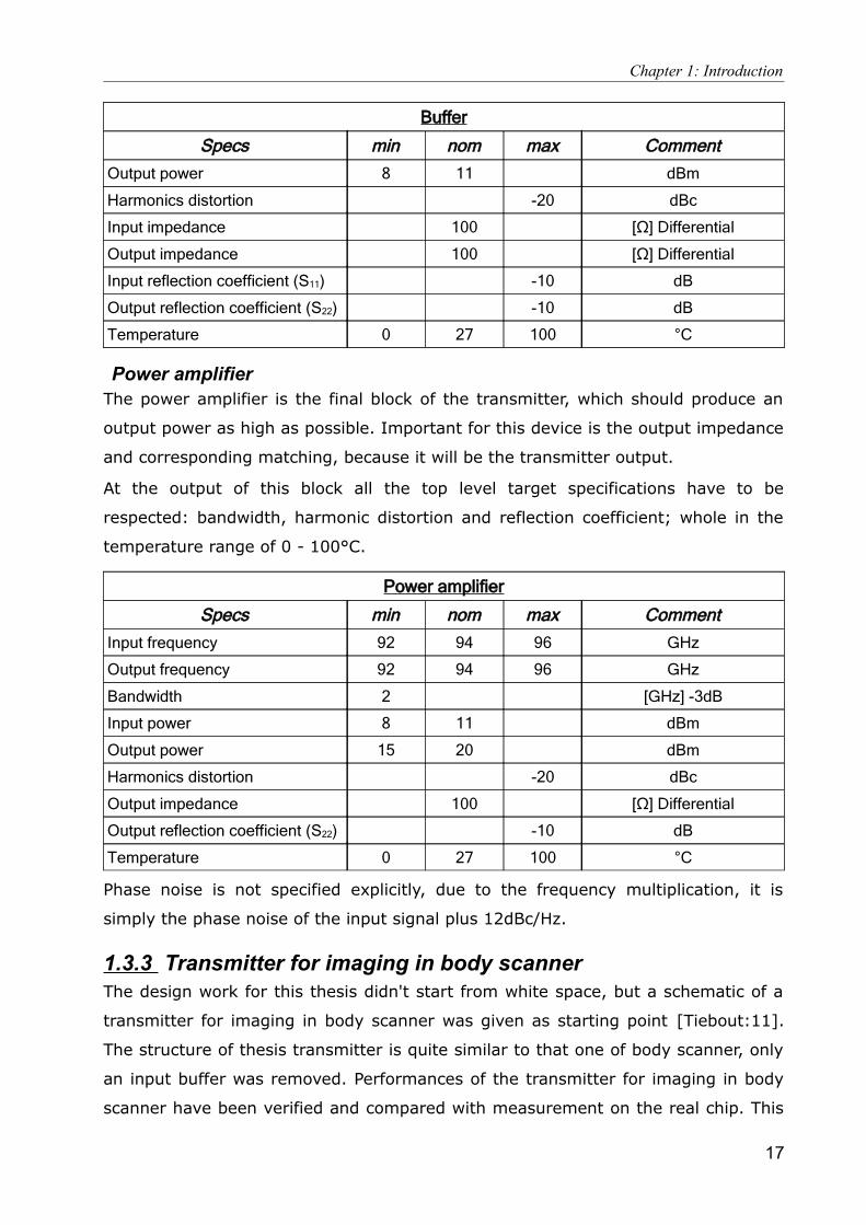
Power amplifierThe power amplifier is the final block of the transmitter, which should produce an
output power as high as possible. Important for this device is the output impedance
and corresponding matching, because it will be the transmitter output.
At the output of this block all the top level target specifications have to be
respected: bandwidth, harmonic distortion and reflection coefficient; whole in the
temperature range of 0 - 100°C.
Power amplifier
Specs min nom max CommentInput frequency 92 94 96 GHz
Output frequency 92 94 96 GHz
Bandwidth 2 [GHz] -3dB
Input power 8 11 dBm
Output power 15 20 dBm
Harmonics distortion -20 dBc
Output impedance 100 [Ω] Differential
Output reflection coefficient (S22) -10 dB
Temperature 0 27 100 °C
Phase noise is not specified explicitly, due to the frequency multiplication, it is
simply the phase noise of the input signal plus 12dBc/Hz.
1.3.3 Transmitter for imaging in body scannerThe design work for this thesis didn't start from white space, but a schematic of a
transmitter for imaging in body scanner was given as starting point [Tiebout:11].
The structure of thesis transmitter is quite similar to that one of body scanner, only
an input buffer was removed. Performances of the transmitter for imaging in body
scanner have been verified and compared with measurement on the real chip. This
17

Chapter 1: Introduction
can let us trust in simulations results.
The working frequency the body scanner applications is roughly 78GHz, and the
used technology is the same Infineon B7HF200, so the distance of this transmitter
from the goal of the thesis is not so great. For these reasons the circuits suggestion
was seriously taken into account, and the schematics of the starting transmitter
have been analysed and than tuned to the goal frequency of the new transmitter.
18
Chapter 2: Technology overview
Chapter 2: Technology overview
In the integrated circuit technologies, BiCMOS (also called BiMOS) refers to the
integration of bipolar junction transistors and CMOS technology into a single
integrated circuit device. Also a pure bipolar integrated circuit technology, as
B7HF200, exists as manufacturing process. These kind of planar processes let to
produce bipolar transistors with very high cut-off frequency (around some hundreds
of GHz), by using some particular construction technique like isolation regions
between adjacent components separated by oxide spacer, emitter and extrinsic
base regions, or self-aligned processing techniques. All these innovative
construction techniques have made these type of products more expensive respect
to CMOS wafers, but also more well performing.
Historically, fabricating both bipolar and metal-oxide-semiconductor (MOS)
transistors in a single integrated circuit proved difficult and expensive. Therefore,
until recently, most of integrated circuits have used one or the other, according to
application requirements [Int:1]. This “all one or the other” choice necessarily
entailed an engineering compromise in many cases, particularly for mixed-signal
integrated circuits. If compared to the ideal case, where the type of each transistor
could be freely and independently chosen according to the function and purpose of
that particular transistor in the circuit (as it can be in circuits built of discrete
components, albeit at much higher cost and size than an integrated circuit design)
it appears as an unpleasant situation.
Bipolar transistors offer high speed, high gain, and low output resistance, which are
excellent properties for high-frequency analog amplifiers, whereas CMOS
technology offers high input resistance and it is excellent for constructing simple,
low-power logic gates.
For as long as the two types of transistors have existed in production, designers of
circuits utilizing discrete components have realized the advantages of integrating
the two technologies. However, lacking an implementation into integrated circuits,
the application of this free-form design was restricted to fairly simple circuits.
Discrete circuits of hundreds or thousands of transistors quickly expand to occupy
hundreds or thousands of square centimetres of circuit board area, and for very
high-speed circuits, such as those used in modern digital computers, the distance
19
Chapter 2: Technology overview
between transistors (and the minimum capacitance of the connections between
them) also makes the desired speeds grossly unattainable, so that if these designs
cannot be built as integrated circuits, then they simply cannot be built.
In the 1990s, modern integrated circuit (IC) fabrication technologies began to make
BiCMOS a reality. This technology rapidly found application in amplifiers and analog
power management circuits, and it has also some advantages in digital logic.
BiCMOS circuits use the characteristics of each type of transistor most
appropriately. Generally this means that high current circuits use metal-oxide-
semiconductor field-effect transistor (MOSFETs) for efficient control, and portions of
specialized very high performance circuits use bipolar devices.
In recent years, improved technology has made possible to combine complimentary
MOS transistors and bipolar devices in a single process at a reasonable cost.
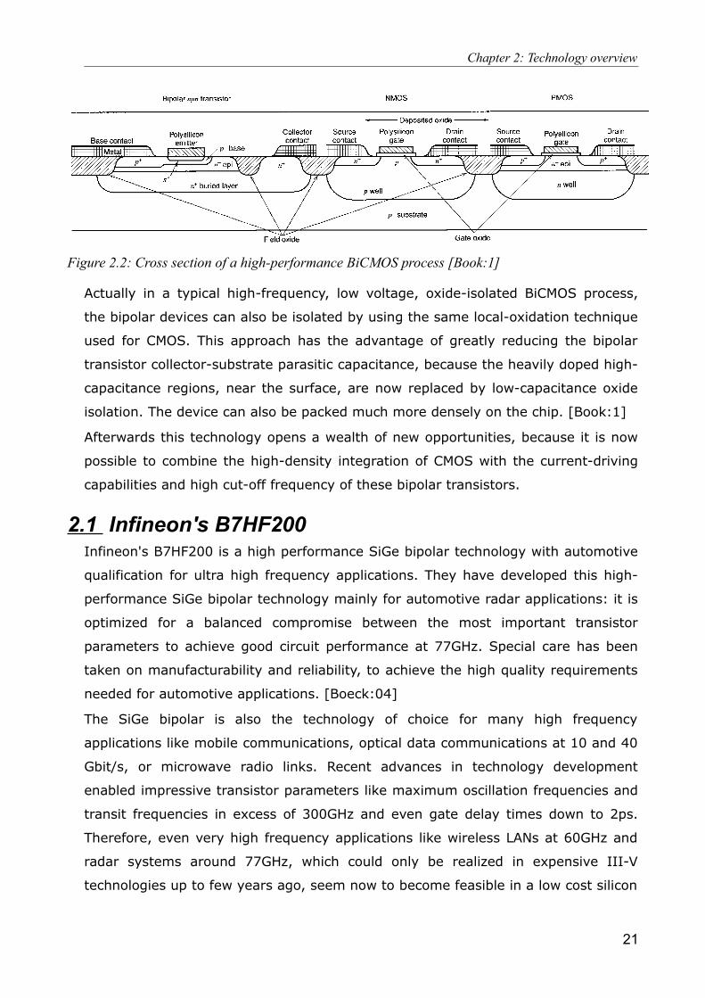
A cross section of a typical BiCMOS process is shown in figure 2.2. A single n-
epitaxial layer is used to implement both the PMOS transistors and bipolar npn
transistors. Its resistivity is chosen so that it can support both devices. An n+ buried
layer is deposited below the epitaxial layer to reduce the collector resistance of the
bipolar device, which simultaneously increases the immunity to latchup. The p-
buried layer (or oxide) between transistors, improves the packing density, because
the collector-collector spacing of the bipolar devices can be reduced. It comes at
the expense of an increased collector-substrate capacitance.
20
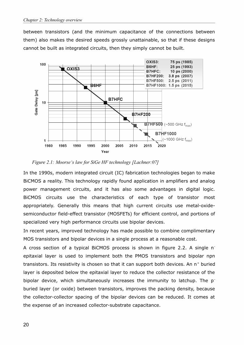
Figure 2.1: Moorse‘s law for SiGe HF technology [Lachner:07]
Chapter 2: Technology overview
Actually in a typical high-frequency, low voltage, oxide-isolated BiCMOS process,
the bipolar devices can also be isolated by using the same local-oxidation technique
used for CMOS. This approach has the advantage of greatly reducing the bipolar
transistor collector-substrate parasitic capacitance, because the heavily doped high-
capacitance regions, near the surface, are now replaced by low-capacitance oxide
isolation. The device can also be packed much more densely on the chip. [Book:1]
Afterwards this technology opens a wealth of new opportunities, because it is now
possible to combine the high-density integration of CMOS with the current-driving
capabilities and high cut-off frequency of these bipolar transistors.
2.1 Infineon's B7HF200Infineon's B7HF200 is a high performance SiGe bipolar technology with automotive
qualification for ultra high frequency applications. They have developed this high-
performance SiGe bipolar technology mainly for automotive radar applications: it is
optimized for a balanced compromise between the most important transistor
parameters to achieve good circuit performance at 77GHz. Special care has been
taken on manufacturability and reliability, to achieve the high quality requirements
needed for automotive applications. [Boeck:04]
The SiGe bipolar is also the technology of choice for many high frequency
applications like mobile communications, optical data communications at 10 and 40
Gbit/s, or microwave radio links. Recent advances in technology development
enabled impressive transistor parameters like maximum oscillation frequencies and
transit frequencies in excess of 300GHz and even gate delay times down to 2ps.
Therefore, even very high frequency applications like wireless LANs at 60GHz and
radar systems around 77GHz, which could only be realized in expensive III-V
technologies up to few years ago, seem now to become feasible in a low cost silicon
21
Figure 2.2: Cross section of a high-performance BiCMOS process [Book:1]
Chapter 2: Technology overview
based technology in a highly integrated manner. Especially radar systems for the
automotive industry could become a new mass market, if the system costs can be
reduced sufficiently.
The B7HF200 technology provides several additional devices to the high speed npn
transistors. Three types of npn devices with different fT - BVCE0 trade-offs are offered
by modifying the collector implant dose, and one vertical pnp. Two poly resistors
with sheet resistances of 150 and 1000Ω/sq. and a TaN thin film resistor with
20Ω/sq. are available. A MIM capacitor with an Al2O3 dielectric and a specific
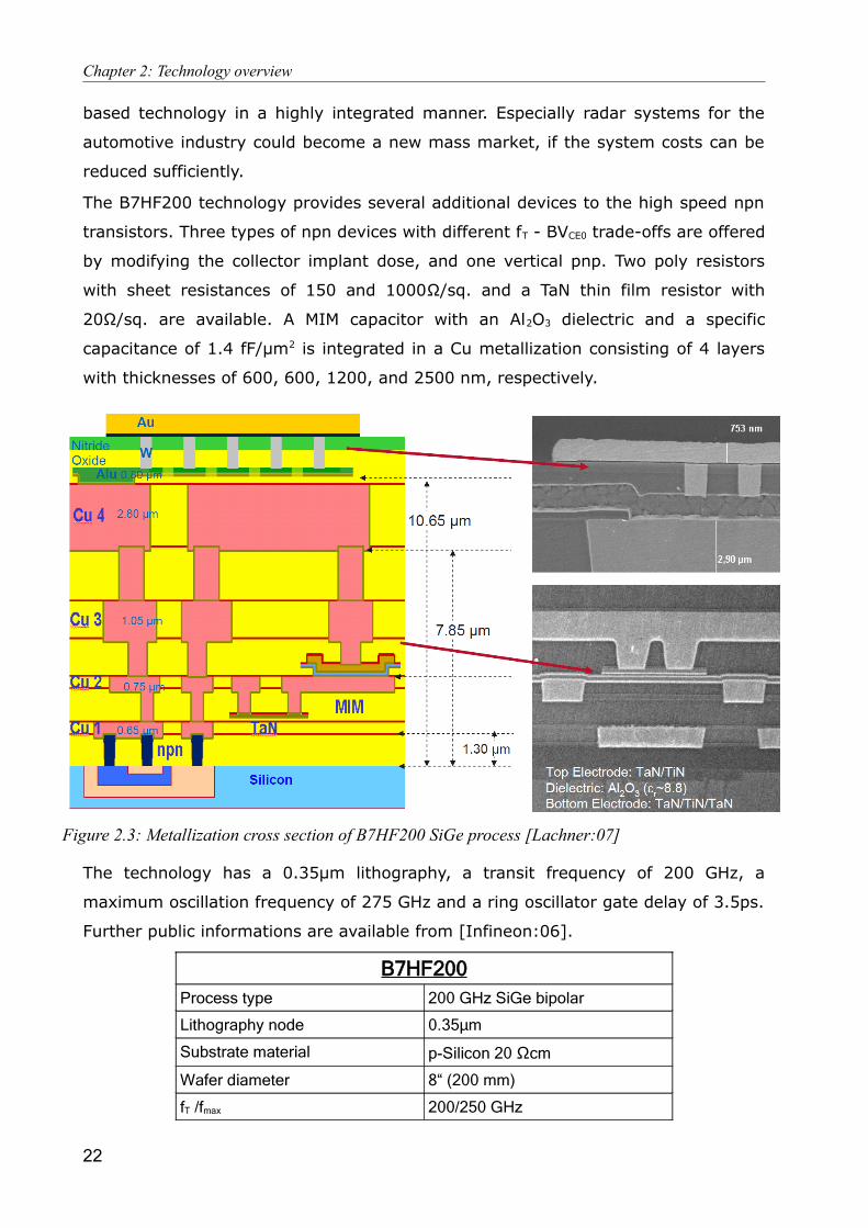
capacitance of 1.4 fF/μm2 is integrated in a Cu metallization consisting of 4 layers
with thicknesses of 600, 600, 1200, and 2500 nm, respectively.
The technology has a 0.35μm lithography, a transit frequency of 200 GHz, a
maximum oscillation frequency of 275 GHz and a ring oscillator gate delay of 3.5ps.
Further public informations are available from [Infineon:06].
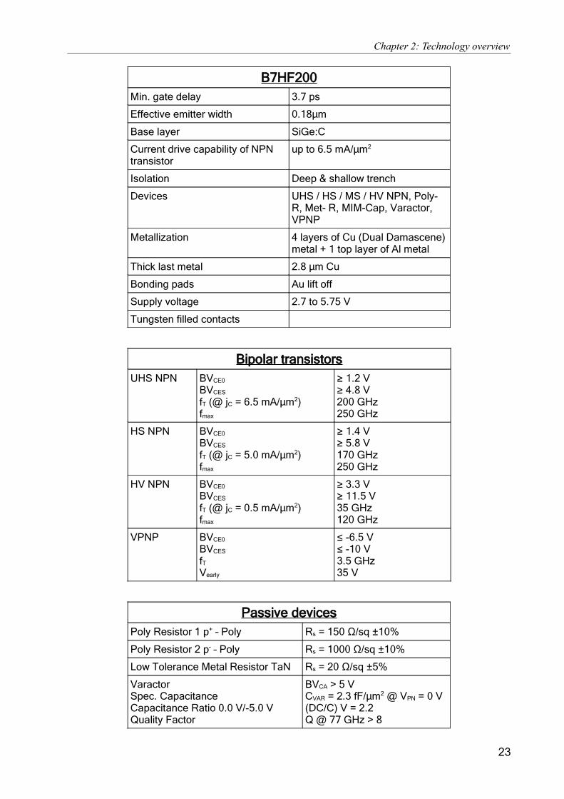
B7HF200Process type 200 GHz SiGe bipolar
Lithography node 0.35μm
Substrate material p-Silicon 20 Ωcm
Wafer diameter 8“ (200 mm)
fT /fmax 200/250 GHz
22
Figure 2.3: Metallization cross section of B7HF200 SiGe process [Lachner:07]
Chapter 2: Technology overview
B7HF200Min. gate delay 3.7 ps
Effective emitter width 0.18μm
Base layer SiGe:C
Current drive capability of NPN transistor
up to 6.5 mA/μm2
Isolation Deep & shallow trench
Devices UHS / HS / MS / HV NPN, Poly-R, Met- R, MIM-Cap, Varactor, VPNP
Metallization 4 layers of Cu (Dual Damascene) metal + 1 top layer of Al metal
Thick last metal 2.8 μm Cu
Bonding pads Au lift off
Supply voltage 2.7 to 5.75 V
Tungsten filled contacts
Bipolar transistorsUHS NPN BVCE0
BVCES
fT (@ jC = 6.5 mA/μm2)fmax
≥ 1.2 V≥ 4.8 V200 GHz250 GHz
HS NPN BVCE0
BVCES
fT (@ jC = 5.0 mA/μm2)fmax
≥ 1.4 V≥ 5.8 V170 GHz250 GHz
HV NPN BVCE0
BVCES
fT (@ jC = 0.5 mA/μm2)fmax
≥ 3.3 V≥ 11.5 V35 GHz120 GHz
VPNP BVCE0
BVCES
fT
Vearly
≤ -6.5 V≤ -10 V3.5 GHz35 V
Passive devicesPoly Resistor 1 p+ – Poly Rs = 150 Ω/sq ±10%
Poly Resistor 2 p– – Poly Rs = 1000 Ω/sq ±10%
Low Tolerance Metal Resistor TaN Rs = 20 Ω/sq ±5%
VaractorSpec. CapacitanceCapacitance Ratio 0.0 V/-5.0 VQuality Factor
BVCA > 5 VCVAR = 2.3 fF/μm2 @ VPN = 0 V(DC/C) V = 2.2Q @ 77 GHz > 8
23
Chapter 2: Technology overview
Passive devicesLinear Capacitor (MIM) -5.5 V < V < +5.5 V
Carea = 1.4 fF/μm2
Q @ 2 GHz > 50Q @ 24 GHz > 25
InductorsCoil dia 135 μm 1.7 nHCoil dia 60 μm 0.25 nH
Q @ 2 GHz > 15Q @ 24 GHz > 20
2.2 Bipolar characteristicsIn the technology used for this transmitter different type of bipolar transistors are
present: high speed npn, high voltage npn and high voltage pnp too. The basic
physical phenomena of these devices are left to specialized theory books, but I will
try to do a short introduction to them, with some graphs of the characteristics.
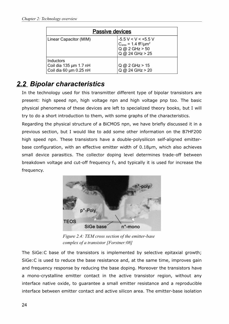
Regarding the physical structure of a BiCMOS npn, we have briefly discussed it in a
previous section, but I would like to add some other information on the B7HF200
high speed npn. These transistors have a double-polysilicon self-aligned emitter-
base configuration, with an effective emitter width of 0.18μm, which also achieves
small device parasitics. The collector doping level determines trade-off between
breakdown voltage and cut-off frequency fT, and typically it is used for increase the
frequency.
The SiGe:C base of the transistors is implemented by selective epitaxial growth;
SiGe:C is used to reduce the base resistance and, at the same time, improves gain
and frequency response by reducing the base doping. Moreover the transistors have
a mono-crystalline emitter contact in the active transistor region, without any
interface native oxide, to guarantee a small emitter resistance and a reproducible
interface between emitter contact and active silicon area. The emitter-base isolation
24
Figure 2.4: TEM cross section of the emitter-basecomplex of a transistor [Forstner:08]
Chapter 2: Technology overview
is improved to increase the base current and the manufacturability of technology.
Given some other information on the structure of SiGe devices, now it will be shown
some measured characteristic about these transistors, which have been got from
some papers. [Boeck:04] [Lachner:07] [Forstner:08]
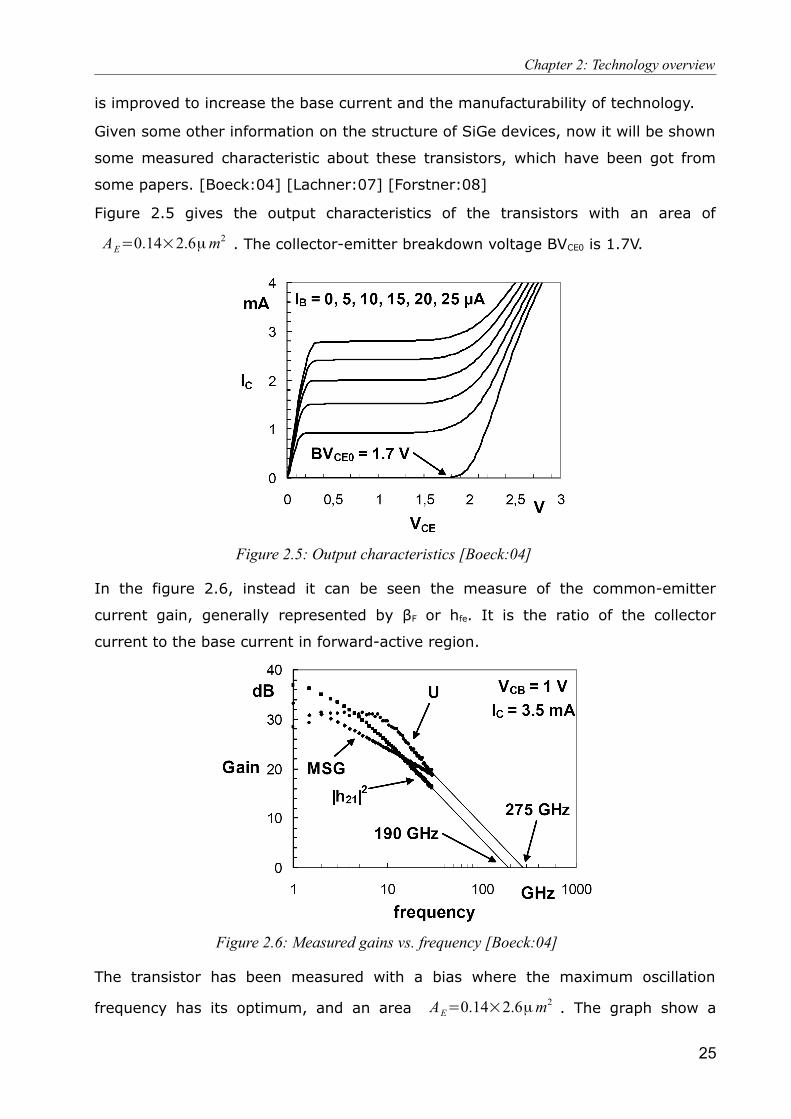
Figure 2.5 gives the output characteristics of the transistors with an area of
AE=0.14×2.6μm2 . The collector-emitter breakdown voltage BVCE0 is 1.7V.
In the figure 2.6, instead it can be seen the measure of the common-emitter
current gain, generally represented by βF or hfe. It is the ratio of the collector
current to the base current in forward-active region.
The transistor has been measured with a bias where the maximum oscillation
frequency has its optimum, and an area AE=0.14×2.6μm2 . The graph show a
25
Figure 2.5: Output characteristics [Boeck:04]
Figure 2.6: Measured gains vs. frequency [Boeck:04]
Chapter 2: Technology overview
decrease of current gain already at 1GHz, with an expected transient frequency
around the 190GHz.
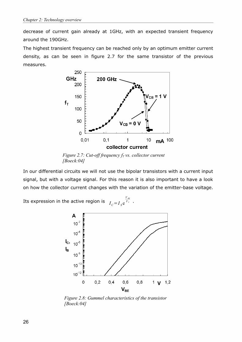
The highest transient frequency can be reached only by an optimum emitter current
density, as can be seen in figure 2.7 for the same transistor of the previous
measures.
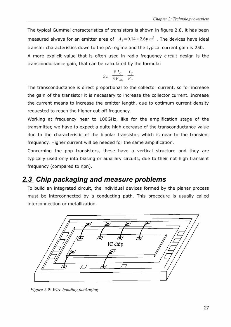
In our differential circuits we will not use the bipolar transistors with a current input
signal, but with a voltage signal. For this reason it is also important to have a look
on how the collector current changes with the variation of the emitter-base voltage.
Its expression in the active region is I C=I S eV BE
V T .
26
Figure 2.8: Gummel characteristics of the transistor [Boeck:04]
Figure 2.7: Cut-off frequency fT vs. collector current [Boeck:04]
Chapter 2: Technology overview
The typical Gummel characteristics of transistors is shown in figure 2.8, it has been
measured always for an emitter area of AE=0.14×2.6μm2 . The devices have ideal
transfer characteristics down to the pA regime and the typical current gain is 250.
A more explicit value that is often used in radio frequency circuit design is the
transconductance gain, that can be calculated by the formula:
g m=∂ I C
∂V BE=
I C
V T
The transconductance is direct proportional to the collector current, so for increase
the gain of the transistor it is necessary to increase the collector current. Increase
the current means to increase the emitter length, due to optimum current density
requested to reach the higher cut-off frequency.
Working at frequency near to 100GHz, like for the amplification stage of the
transmitter, we have to expect a quite high decrease of the transconductance value
due to the characteristic of the bipolar transistor, which is near to the transient
frequency. Higher current will be needed for the same amplification.
Concerning the pnp transistors, these have a vertical structure and they are
typically used only into biasing or auxiliary circuits, due to their not high transient
frequency (compared to npn).
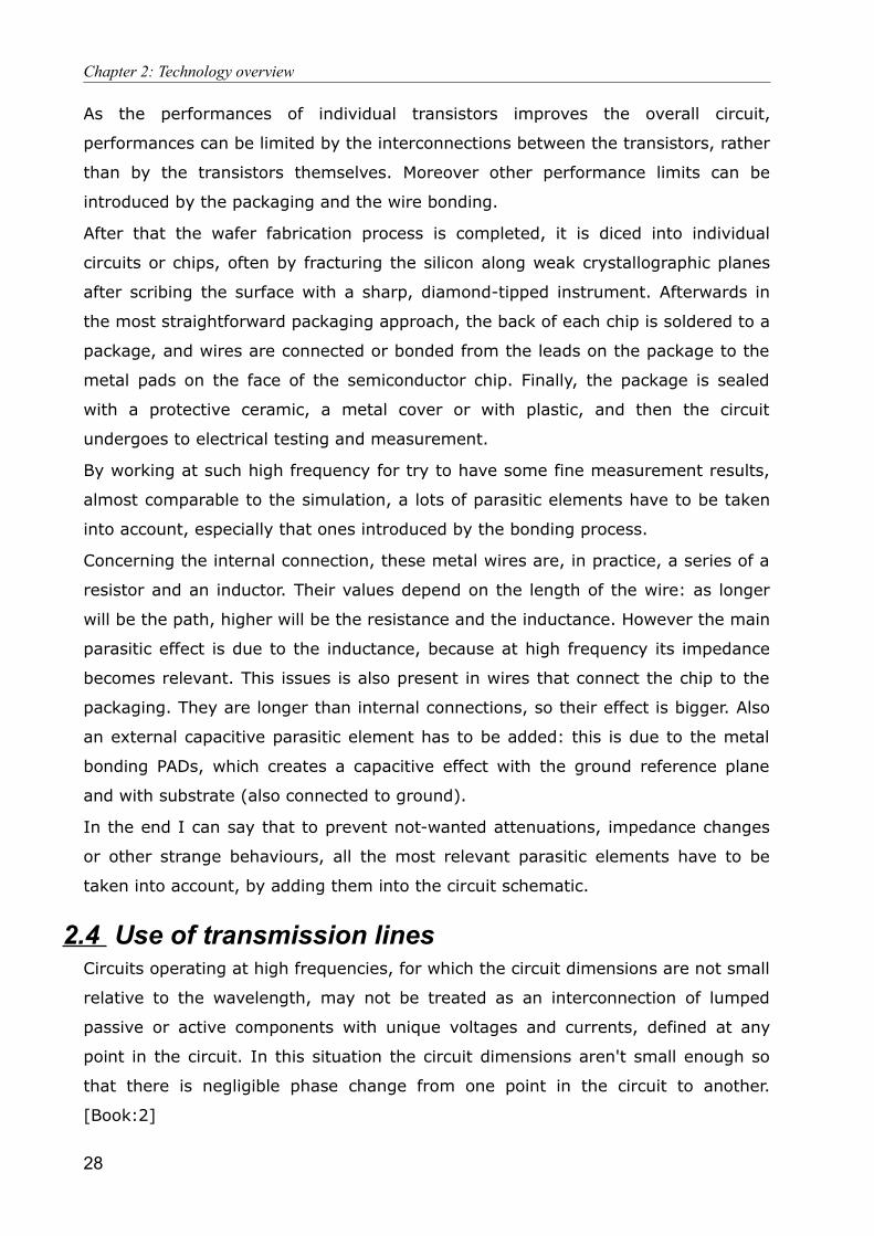
2.3 Chip packaging and measure problemsTo build an integrated circuit, the individual devices formed by the planar process
must be interconnected by a conducting path. This procedure is usually called
interconnection or metallization.
27
Figure 2.9: Wire bonding packaging
Chapter 2: Technology overview
As the performances of individual transistors improves the overall circuit,
performances can be limited by the interconnections between the transistors, rather
than by the transistors themselves. Moreover other performance limits can be
introduced by the packaging and the wire bonding.
After that the wafer fabrication process is completed, it is diced into individual
circuits or chips, often by fracturing the silicon along weak crystallographic planes
after scribing the surface with a sharp, diamond-tipped instrument. Afterwards in
the most straightforward packaging approach, the back of each chip is soldered to a
package, and wires are connected or bonded from the leads on the package to the
metal pads on the face of the semiconductor chip. Finally, the package is sealed
with a protective ceramic, a metal cover or with plastic, and then the circuit
undergoes to electrical testing and measurement.
By working at such high frequency for try to have some fine measurement results,
almost comparable to the simulation, a lots of parasitic elements have to be taken
into account, especially that ones introduced by the bonding process.
Concerning the internal connection, these metal wires are, in practice, a series of a
resistor and an inductor. Their values depend on the length of the wire: as longer
will be the path, higher will be the resistance and the inductance. However the main
parasitic effect is due to the inductance, because at high frequency its impedance
becomes relevant. This issues is also present in wires that connect the chip to the
packaging. They are longer than internal connections, so their effect is bigger. Also
an external capacitive parasitic element has to be added: this is due to the metal
bonding PADs, which creates a capacitive effect with the ground reference plane
and with substrate (also connected to ground).
In the end I can say that to prevent not-wanted attenuations, impedance changes
or other strange behaviours, all the most relevant parasitic elements have to be
taken into account, by adding them into the circuit schematic.
2.4 Use of transmission linesCircuits operating at high frequencies, for which the circuit dimensions are not small
relative to the wavelength, may not be treated as an interconnection of lumped
passive or active components with unique voltages and currents, defined at any
point in the circuit. In this situation the circuit dimensions aren't small enough so
that there is negligible phase change from one point in the circuit to another.
[Book:2]
28
Chapter 2: Technology overview
From the electromagnetic and transmission line theories we know that in some
situations we can have a signal reflection due to a load mismatch. Besides, in order
to deliver the maximum power to the load we must have an impedance matching,
which means that the impedance seen from the load, toward the circuits, has to be
complex conjugate of the load Z m=Z l* .
Typical matching networks used at high frequency are the “lumped elements
matching network”, which are made of reactive elements as capacitors and
inductors (L-network, ∏-network, T-network) [Book:3]. Passing the 10 or 20 GHz
the sizes of lumped elements become comparable to the use of transmission line as
matching networks. In particular the inductors construction is the main problem,
because with the increasing of the frequency we have more electromagnetic
interferences and less component's quality factor, due to parasitic element,
tolerance or mismatch increasing.
Afterwards in the EHF and in the last part of SHF bandwidths, the matching
networks are made with planar transmission lines for integrate circuits. Typically
this networks are single-stub shunt tuning, double-stub tuning or other similar
configurations, whose theory and designing rules can be found on the theory books
[Book:2].
Integrated circuits transmission lines are also used to connect different device on
the same wafer, where possible. This happen because at high frequency the
behaviour of a transmission line is much more comprehensible and reliable than a
simple wire of metal, whose electrical characteristic (usually inductive) can be
influenced by electromagnetic coupling or other parasitic effects due to the
components around it.
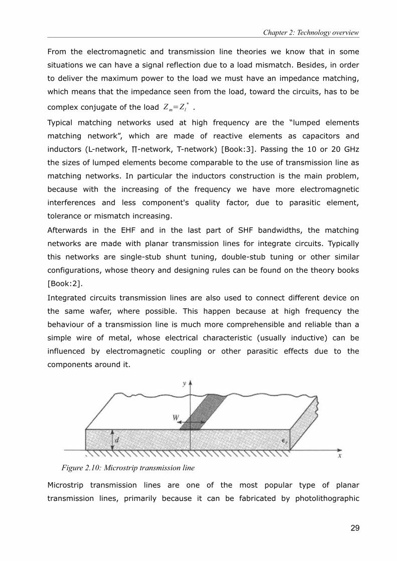
Microstrip transmission lines are one of the most popular type of planar
transmission lines, primarily because it can be fabricated by photolithographic
29
Figure 2.10: Microstrip transmission line
Chapter 2: Technology overview
processes and it is easily integrated with other passive and active microwave
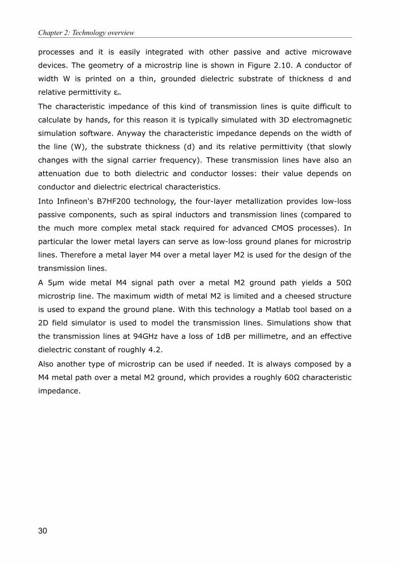
devices. The geometry of a microstrip line is shown in Figure 2.10. A conductor of
width W is printed on a thin, grounded dielectric substrate of thickness d and
relative permittivity εr.
The characteristic impedance of this kind of transmission lines is quite difficult to
calculate by hands, for this reason it is typically simulated with 3D electromagnetic
simulation software. Anyway the characteristic impedance depends on the width of
the line (W), the substrate thickness (d) and its relative permittivity (that slowly
changes with the signal carrier frequency). These transmission lines have also an
attenuation due to both dielectric and conductor losses: their value depends on
conductor and dielectric electrical characteristics.
Into Infineon's B7HF200 technology, the four-layer metallization provides low-loss
passive components, such as spiral inductors and transmission lines (compared to
the much more complex metal stack required for advanced CMOS processes). In
particular the lower metal layers can serve as low-loss ground planes for microstrip
lines. Therefore a metal layer M4 over a metal layer M2 is used for the design of the
transmission lines.
A 5μm wide metal M4 signal path over a metal M2 ground path yields a 50Ω
microstrip line. The maximum width of metal M2 is limited and a cheesed structure
is used to expand the ground plane. With this technology a Matlab tool based on a
2D field simulator is used to model the transmission lines. Simulations show that
the transmission lines at 94GHz have a loss of 1dB per millimetre, and an effective
dielectric constant of roughly 4.2.
Also another type of microstrip can be used if needed. It is always composed by a
M4 metal path over a metal M2 ground, which provides a roughly 60Ω characteristic
impedance.
30
Chapter 3: Input network
Chapter 3: Input network
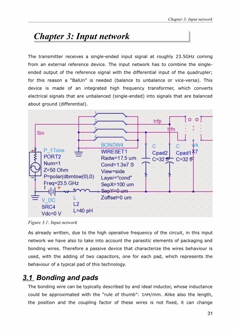
The transmitter receives a single-ended input signal at roughly 23.5GHz coming
from an external reference device. The input network has to combine the single-
ended output of the reference signal with the differential input of the quadrupler;
for this reason a “BalUn” is needed (balance to unbalance or vice-versa). This
device is made of an integrated high frequency transformer, which converts
electrical signals that are unbalanced (single-ended) into signals that are balanced
about ground (differential).
As already written, due to the high operative frequency of the circuit, in this input
network we have also to take into account the parasitic elements of packaging and
bonding wires. Therefore a passive device that characterize the wires behaviour is
used, with the adding of two capacitors, one for each pad, which represents the
behaviour of a typical pad of this technology.
3.1 Bonding and padsThe bonding wire can be typically described by and ideal inductor, whose inductance
could be approximated with the “rule of thumb”: 1nH/mm. Alike also the length,
the position and the coupling factor of these wires is not fixed, it can change
31
Figure 3.1: Input network
Chapter 3: Input network
according to the geometric bonding schemes. For these reasons to estimate a
general-purpose and reliable model is quite difficult. However, given that bonding
wires and packages are quite the same for most of the measured circuits, some
trials for doing a faithful model has been made by me and also historically.
In the first trial it has been simply inserted an ideal inductance in place of the wire,
and considering the path length roughly 2mm, its value has been set to 2nH. Also
other similar trials have been made, but without any type of comparison with the
real behaviour, there wasn't a high probability that they will work.
The latest and more trusted model was an evaluation with an S-parameter 3D-EM
simulation from 10GHz to 30GHz, which gave a file to use in simulation analysis. At
this purpose, for playing fair, the S-parameter file can't be used directly into the
schematic, because the Spectre simulator fit it in a wrong way and get some
strange behaviour on the model. An alternative was therefore needed. It was made
introducing an auxiliary block of ADS (Advanced design system) used for bonding
structures. All this last work was made by Delft University of Technology [Int:2],
[Mouthaan:97], [Harm:98]. This model simply takes the geometrical data of the
bondwires and the result is easily usable in ADS, so that I could focus on the active
circuits.
Concerning the pads, these are a metallized area on the surface of a semiconductor
device, to which connections are made. Typically the bonding pad can be made of
all the metal layers stacked on top of each other, and connected through vias. This
arrangement allows connection from the core of the chip to the pad and, in turn, to
the outside world using any metal layer. Anyway only at the “top-metal” is required
to create a connection with the bonding wire.
The size of these metallic areas is usually prearranged by the used technology, even
if it can be chosen among two or more lateral length, on necessity. If high current
might pass in the pad, it has to be larger, also for reduce the parasitic resistance
and increasing the reliability of bonding contact. However a bigger area means a
higher parasitic capacitance, which is the most annoying and relevant parasitic
behaviour for these devices at high frequency. The value of the capacitance, toward
ground, is also influenced by the distance from the ground plane or substrate (also
connected to ground), so by the number of metal layers that compose the pad.
In my layouts, with the B7HF200 technology, it has been used pads with size of
68x68μm2 or 68x86μm2. The smallest size should be used for signal path, instead
32
Chapter 3: Input network
the largest for ground and supply voltage contacts. The value of the capacitor can
be calculated with the specific oxide capacitances for area plus the edge one, which
are reported on the technology's general specifications. At this purpose also a
simulation of the pad device can be used. I got a nominal value of 25fF for a size of
68x68μm2 and 32fF for the largest one: the difference between them is not so high.
As we will see, it has been decided to use the smallest size only at the output of the
transmitter, because there the frequency is higher than at the input, so more
susceptible to parasitic effect, so the capacitance decrease could be justified.
Anyhow we have to take into account a fitted capacitor for each pad.
3.2 TransformerIn this section we will not treat in deep how to make or to choose an integrated
circuit transformer and neither how to fit a good lumped model for it, but I refer to
the large literature on this topic: books and IEEE papers [Book:3], [Biondi:06],
[Scuderi:04], [Laskin:08], [Gan:06].
The main aim of the high frequency integrated transformer of this transmitter, is to
convert a single-ended input signal into a differential signal. This passive device has
been preferred to other methods of single-ended to differential conversion, such as
differential pairs, since it do not consume any DC power. Furthermore, due to their
symmetry, transformers have better common mode rejection than differential pairs
at mm-wave frequencies.
Unfortunately to use an integrated circuit transformer it is necessary a quite big
area, because it is typically composed by two overlapped or very close metal path,
of two near metal layer. The structures could be also more complicated, in order to
imitate the windings of a low frequency transformer. This type of construction aids
the electromagnetic coupling between the primary and secondary metal path, to
the purpose of increase the power transfer.
The area within the transformer has to be kept free from any other devices,
because they could create some interferences or increase its losses. Moreover also
the substrate should avoid any interferences, so a “wall” of substrate contacts is
placed around the transformer and connected to ground.
3.2.1 Choice of transformerThe choice of which type of transformer has to be used in the transmitter was quite
easy, in my case. I haven't been in need of design anyone of it, given that 5
33
Chapter 3: Input network
transformers were available as library; they covered different purpose around the
input frequency of 23.5GHz. All these devices were been used in other circuits, and
for each one a reliable S-parameter file describes their behaviour. For this reason
only a comparison of their characteristics was needed, with the choice of the most
suitable for the circuit goal.
All the proposed transformers are optimized for a wide bandwidth. They have a
stacked configuration to maximise the coupling coefficient, and a secondary-to-
primary turns ratio of 1. The only structural changes among them are the
dimensions and the number of spins:
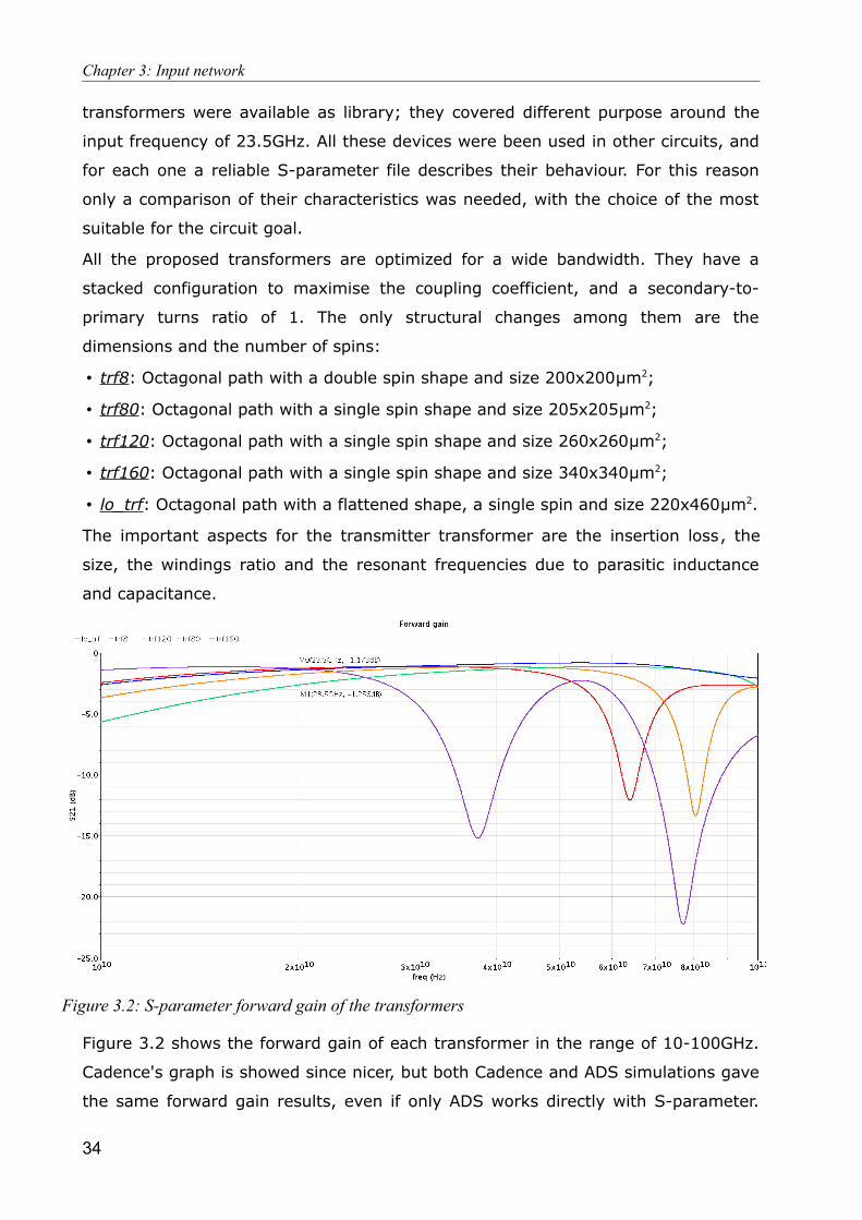
• trf8 : Octagonal path with a double spin shape and size 200x200μm2;
• trf80 : Octagonal path with a single spin shape and size 205x205μm2;
• trf120 : Octagonal path with a single spin shape and size 260x260μm2;
• trf160 : Octagonal path with a single spin shape and size 340x340μm2;
• lo_trf : Octagonal path with a flattened shape, a single spin and size 220x460μm2.
The important aspects for the transmitter transformer are the insertion loss, the
size, the windings ratio and the resonant frequencies due to parasitic inductance
and capacitance.
Figure 3.2 shows the forward gain of each transformer in the range of 10-100GHz.
Cadence's graph is showed since nicer, but both Cadence and ADS simulations gave
the same forward gain results, even if only ADS works directly with S-parameter.
34
Figure 3.2: S-parameter forward gain of the transformers
Chapter 3: Input network
The simulation was made without any tuning capacitor or load, but with only the
simulation ports setted to 50Ω and with the input one connected also to ground.
This should show the behaviour of the transformer, which acts like a single-ended to
differential converter.
Typically, by adding a shunt capacitor at one of the two ports, we can decrease the
resonant frequency and, in some situation, to have a better forward gain into the
interest frequency range. Therefore, for the choice, I have kept into account the
resonant frequency, which has to be quite higher then operating frequency, and the
forward gain, that hasn’t to be too much low. Afterwards the forward characteristics
can be slightly changed by adding a load and tuning an appropriate capacitor.
All transformers, except “trf8”, have good electrical characteristics for our purpose;
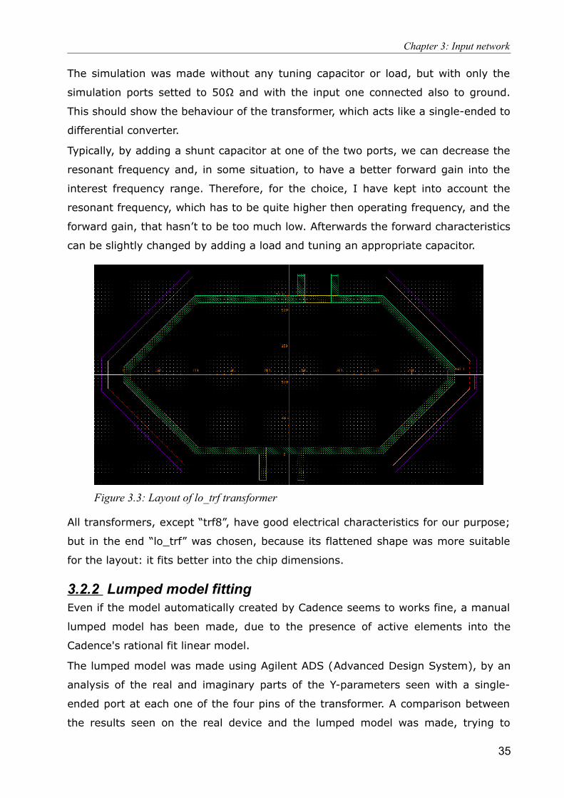
but in the end “lo_trf” was chosen, because its flattened shape was more suitable
for the layout: it fits better into the chip dimensions.
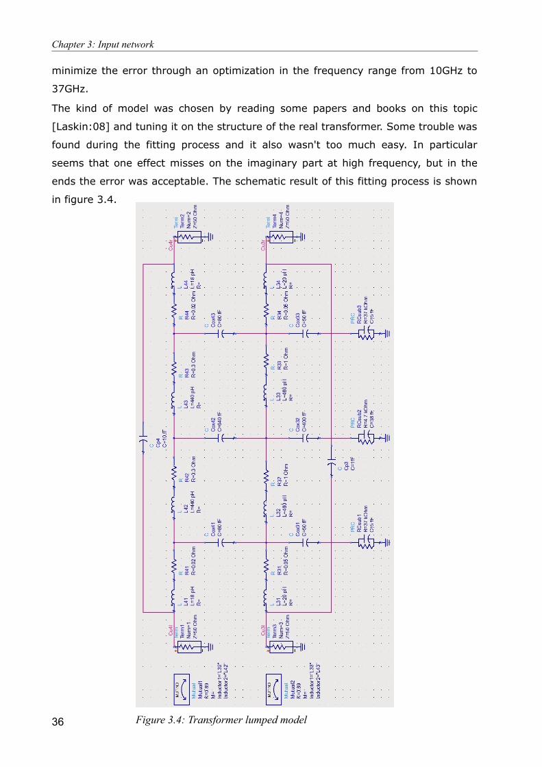
3.2.2 Lumped model fittingEven if the model automatically created by Cadence seems to works fine, a manual
lumped model has been made, due to the presence of active elements into the
Cadence's rational fit linear model.
The lumped model was made using Agilent ADS (Advanced Design System), by an
analysis of the real and imaginary parts of the Y-parameters seen with a single-
ended port at each one of the four pins of the transformer. A comparison between
the results seen on the real device and the lumped model was made, trying to
35
Figure 3.3: Layout of lo_trf transformer
Chapter 3: Input network
minimize the error through an optimization in the frequency range from 10GHz to
37GHz.
The kind of model was chosen by reading some papers and books on this topic
[Laskin:08] and tuning it on the structure of the real transformer. Some trouble was
found during the fitting process and it also wasn't too much easy. In particular
seems that one effect misses on the imaginary part at high frequency, but in the
ends the error was acceptable. The schematic result of this fitting process is shown
in figure 3.4.
36 Figure 3.4: Transformer lumped model
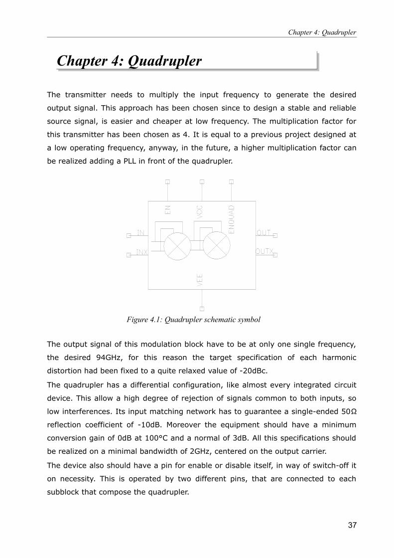
Chapter 4: Quadrupler
Chapter 4: Quadrupler
The transmitter needs to multiply the input frequency to generate the desired
output signal. This approach has been chosen since to design a stable and reliable
source signal, is easier and cheaper at low frequency. The multiplication factor for
this transmitter has been chosen as 4. It is equal to a previous project designed at
a low operating frequency, anyway, in the future, a higher multiplication factor can
be realized adding a PLL in front of the quadrupler.
The output signal of this modulation block have to be at only one single frequency,
the desired 94GHz, for this reason the target specification of each harmonic
distortion had been fixed to a quite relaxed value of -20dBc.
The quadrupler has a differential configuration, like almost every integrated circuit
device. This allow a high degree of rejection of signals common to both inputs, so
low interferences. Its input matching network has to guarantee a single-ended 50Ω
reflection coefficient of -10dB. Moreover the equipment should have a minimum
conversion gain of 0dB at 100°C and a normal of 3dB. All this specifications should
be realized on a minimal bandwidth of 2GHz, centered on the output carrier.
The device also should have a pin for enable or disable itself, in way of switch-off it
on necessity. This is operated by two different pins, that are connected to each
subblock that compose the quadrupler.
37
Figure 4.1: Quadrupler schematic symbol
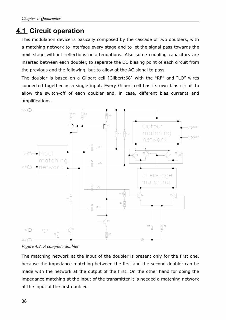
Chapter 4: Quadrupler
4.1 Circuit operationThis modulation device is basically composed by the cascade of two doublers, with
a matching network to interface every stage and to let the signal pass towards the
next stage without reflections or attenuations. Also some coupling capacitors are
inserted between each doubler, to separate the DC biasing point of each circuit from
the previous and the following, but to allow at the AC signal to pass.
The doubler is based on a Gilbert cell [Gilbert:68] with the “RF” and “LO” wires
connected together as a single input. Every Gilbert cell has its own bias circuit to
allow the switch-off of each doubler and, in case, different bias currents and
amplifications.
The matching network at the input of the doubler is present only for the first one,
because the impedance matching between the first and the second doubler can be
made with the network at the output of the first. On the other hand for doing the
impedance matching at the input of the transmitter it is needed a matching network
at the input of the first doubler.
38
Figure 4.2: A complete doubler
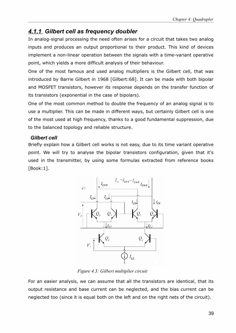
Chapter 4: Quadrupler
4.1.1 Gilbert cell as frequency doublerIn analog-signal processing the need often arises for a circuit that takes two analog
inputs and produces an output proportional to their product. This kind of devices
implement a non-linear operation between the signals with a time-variant operative
point, which yields a more difficult analysis of their behaviour.
One of the most famous and used analog multipliers is the Gilbert cell, that was
introduced by Barrie Gilbert in 1968 [Gilbert:68]. It can be made with both bipolar
and MOSFET transistors, however its response depends on the transfer function of
its transistors (exponential in the case of bipolars).
One of the most common method to double the frequency of an analog signal is to
use a multiplier. This can be made in different ways, but certainly Gilbert cell is one
of the most used at high frequency, thanks to a good fundamental suppression, due
to the balanced topology and reliable structure.
Gilbert cellBriefly explain how a Gilbert cell works is not easy, due to its time variant operative
point. We will try to analyse the bipolar transistors configuration, given that it's
used in the transmitter, by using some formulas extracted from reference books
[Book:1].
For an easier analysis, we can assume that all the transistors are identical, that its
output resistance and base current can be neglected, and the bias current can be
neglected too (since it is equal both on the left and on the right nets of the circuit).
39
Figure 4.3: Gilbert multiplier circuit

Chapter 4: Quadrupler
A transistor, of an emitter couple pair, produces a collector current, related to the
differential input voltage, that in the case of Q1 and Q2 can be expressed as:
I C1=I EE
1+exp(−V 2
V T ) ; I C2=
I EE
1+exp( V 2
V T )Where VT is the thermal voltage. The same consideration can be made for all the
other bipolar transistors:
I C3=I C1
1+exp( V 1
V T ) ; I C4=
I C1
1+exp(− V 1
V T ) ; I C5=
I C2
1+exp(−V 1
V T ) ; I C6=
I C2
1+exp(V 1
V T )Combining all these formulas to obtain the expressions for the collector currents of
the upper stage, we get:
I C3=I EE
[1+exp( V 1
V T )]⋅[1+exp(−V 2
V T )] ; I C4=
I EE
[1+exp(−V 1
V T )]⋅[1+exp(−V 2
V T )]I C5=
I EE
[1+exp(−V 1
V T )]⋅[1+exp(V 2
V T )] ; I C6=
I EE
[1+exp( V 1
V T )]⋅[1+exp( V 2
V T )]The differential output current is then given by:
Δ I= I C3−5− I C4−6=I C3+I C5−( I C4+I C6)=( I C3−I C6)−(I C4− I C5)
= I EE [tanh( V 1
2 V T )][ tanh( V 2
2 V T )]The DC transfer characteristic, then, is the product of the hyperbolic tangent of the
two input voltages.
If the magnitude of V1 and V2 are kept small with respect to VT, the hyperbolic
tangent function can be approximated as linear and the circuit behaves as a
multiplier, developing the product of V1 and V2. However, by including non-linearity
to compensate for the hyperbolic tangent function in series with each input, the
range of input voltages over which linearity is maintained can be greatly extended.
This technique is used in so-called four-quadrant analog multipliers.
Frequency doublerThe multiplication of two different signal can be expressed, for simplicity, as the
multiplication of two cosines. The result of this operation can be calculated by the
trigonometric formulas, and gives:
40
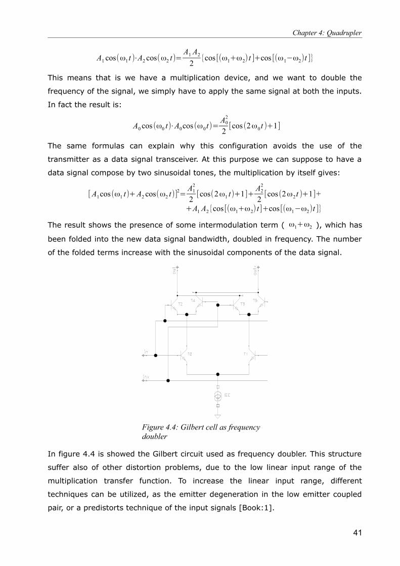
Chapter 4: Quadrupler
A1 cos(ω1t )⋅A2 cos(ω2 t)=A1 A2
2cos [(ω1+ω2) t ]+cos [(ω1−ω2)t ]
This means that is we have a multiplication device, and we want to double the
frequency of the signal, we simply have to apply the same signal at both the inputs.
In fact the result is:
A0 cos (ω0 t)⋅A0cos (ω0t)=A0
2
2[cos (2ω0t )+1]
The same formulas can explain why this configuration avoids the use of the
transmitter as a data signal transceiver. At this purpose we can suppose to have a
data signal compose by two sinusoidal tones, the multiplication by itself gives:
[A1cos(ω1 t)+A2 cos(ω2 t)]2=A1
2
2[cos(2ω1 t)+1]+
A22
2[cos(2ω2t )+1]+
+A1 A2 cos [(ω1+ω2) t ]+cos [(ω1−ω2)t ]
The result shows the presence of some intermodulation term ( ω1+ω2 ), which has
been folded into the new data signal bandwidth, doubled in frequency. The number
of the folded terms increase with the sinusoidal components of the data signal.
In figure 4.4 is showed the Gilbert circuit used as frequency doubler. This structure
suffer also of other distortion problems, due to the low linear input range of the
multiplication transfer function. To increase the linear input range, different
techniques can be utilized, as the emitter degeneration in the low emitter coupled
pair, or a predistorts technique of the input signals [Book:1].
41
Figure 4.4: Gilbert cell as frequency doubler
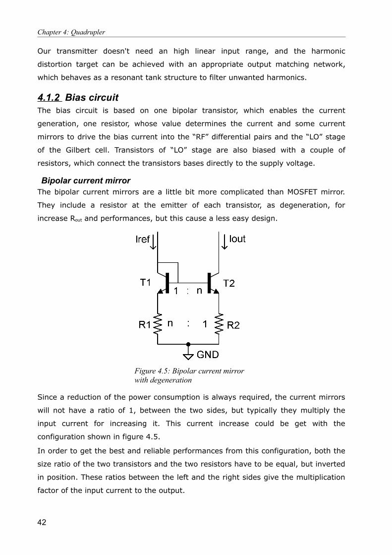
Chapter 4: Quadrupler
Our transmitter doesn't need an high linear input range, and the harmonic
distortion target can be achieved with an appropriate output matching network,
which behaves as a resonant tank structure to filter unwanted harmonics.
4.1.2 Bias circuitThe bias circuit is based on one bipolar transistor, which enables the current
generation, one resistor, whose value determines the current and some current
mirrors to drive the bias current into the “RF” differential pairs and the “LO” stage
of the Gilbert cell. Transistors of “LO” stage are also biased with a couple of
resistors, which connect the transistors bases directly to the supply voltage.
Bipolar current mirrorThe bipolar current mirrors are a little bit more complicated than MOSFET mirror.
They include a resistor at the emitter of each transistor, as degeneration, for
increase Rout and performances, but this cause a less easy design.
Since a reduction of the power consumption is always required, the current mirrors
will not have a ratio of 1, between the two sides, but typically they multiply the
input current for increasing it. This current increase could be get with the
configuration shown in figure 4.5.
In order to get the best and reliable performances from this configuration, both the
size ratio of the two transistors and the two resistors have to be equal, but inverted
in position. These ratios between the left and the right sides give the multiplication
factor of the input current to the output.
42
Figure 4.5: Bipolar current mirror with degeneration

Chapter 4: Quadrupler
To analyse it, we can suppose that βF≫1 and write the following formula:
I out=R1
R2⋅I ref +
V T
R2ln( I ref
I out
I S2
I S1)If for example the emitter area of T2 is n time that one of T1 ( T 2=n⋅T 1 ), we have
that I S2=n⋅I S1 , and with the same ratio in the resistors value R1=n⋅R2 , we get
I out≈n⋅I ref .
Complete circuitWritten as a bipolar current mirror works, it can be explained how the bias and
enable circuit works. It can be seen completely in figure 4.6.
The enable is achieved with a simple bipolar transistor with the base connected
directly to ground. When activated, T0 works in the saturation region and lets to the
current to pass across the resistor R2 into the PNP current mirror. The current here
generated can be calculated supposing an emitter-base voltage of V BE=0.8V and
a saturation emitter-collector voltage of V CEsat=0.25V :
I≈(V CC−V BE−V CEsat)
(R2+R3)= 2.25(R2+R3)
43
Figure 4.6: Biasing and enable circuit of the doubler
Chapter 4: Quadrupler
The PNP current mirror reproduces the input current multiplied by 2, even if the
ratio of the transistors is not exactly respected. This is due to the only two sizes
allowed for the PNP of this technology. However, as it has been seen, the mirror
multiplication factor is determined, for most, by the resistors ratio that in this case
is 2.
The current mirrored and doubled, enters into another mirror. This one is composed
by T3 and the parallel of the two transistor of the Gilbert cell “RF” stage (T4, T5).
Resistors R8 e R9 can be neglected for the mirror behaviour, because they simply
match the DC bias with the RF signal. Therefore the NPN mirror allow the biasing of
the Gilbert cell. To determine the multiplication factor, the emitter length of the two
“RF” transistors of the Gilbert cell have to be summed and then divided by the
emitter length of T3. This value has also to be setted on the ratio between R6 and R7.
In the end, resistor R4 brings the bases of the two PNP to VCC when transistors T0 is
switched-off.
The transistors bases of the “LO” stage, to keep the bias current, have to be
connected to an appropriate voltage. This voltage could determine the maximum
output voltage swing for the signal, so it has to be chosen according to the
maximum output power to reach. In the quadrupler the highest output power
allows us to connect the bases directly to the voltage supply; obviously through a
resistor, to match the DC bias with the AC signal. The value of these resistors is not
fundamental, but certainly it can't be too high or too low, so it has been chosen
R10=R11=500Ω . The same type of considerations are valid also for R8=R9=500Ω .
Further capacitors have been added at each input of the Gilbert cell to separate the
bias voltage of the “LO” and “RF” transistors bases and to allow at signal coming
from the transformer to pass. Their values have to be chosen according to the
frequency of the input signal, which must pass through them without relevant
attenuations.
4.2 Design to 94GHzTo design the quadrupler at 94GHz, and more in general all the high frequency
devices, is quite tricky. It requires to take into account, at the same time, all the
specifications to reach, because every variation of one component value, to achieve
a particular issue, it might change and make worse another specification. For this
reason many design iterations based on a large number of simulations were
performed to get a good solution.
44
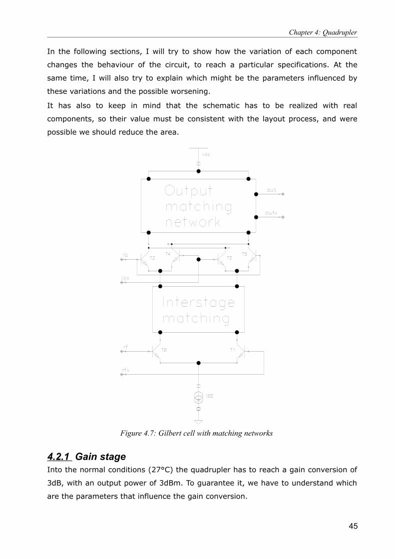
Chapter 4: Quadrupler
In the following sections, I will try to show how the variation of each component
changes the behaviour of the circuit, to reach a particular specifications. At the
same time, I will also try to explain which might be the parameters influenced by
these variations and the possible worsening.
It has also to keep in mind that the schematic has to be realized with real
components, so their value must be consistent with the layout process, and were
possible we should reduce the area.
4.2.1 Gain stageInto the normal conditions (27°C) the quadrupler has to reach a gain conversion of
3dB, with an output power of 3dBm. To guarantee it, we have to understand which
are the parameters that influence the gain conversion.
45
Figure 4.7: Gilbert cell with matching networks
Chapter 4: Quadrupler
Considering only the Gilbert cell and its matching networks (figure 4.7), the
differential input signal is applied to the bases of the “RF” differential pairs. Here
the voltage is converted into current by the bipolar transistors, with a conversion
gain due to the transconductance of the bipolar ( g m ). This element can be
increased or decreased through the variation of the bias current which flows across
the transistors. How to change the bias current was explained in a previous section
on this chapter. It has to be remembered that every bipolar has a maximum current
density, which has to be respected to avoid unexpected behaviours.
From the collector of the lower transistors, the current flows across the interstage
matching network toward the “LO” stage. Into this intermediate network we can
suppose that the current losses are negligible, but some reflection of power might
happen. Determine this reflection coefficient, in order to estimate the effective
current amplitude, is difficult, because we should know the exact value of the
impedances seen from the collector and the emitter of the two transistors.
Moreover there isn't a clear impedance matching, so more reflection waves are
added together in the final result. However to get the best power transfer it can be
made the interstage matching, which will be explained in the following section.
Also determine the exact gain contribute of the “LO” stage is quite difficult, in
particular at high frequencies. From the literature [Book:3] we know that if we can
consider each differential pair, alternatively, completely on or off (like commanded
by a square wave), the gain contribute is 2π . Even if due to the high amplitude of
the command signal we could trust in the previous supposition, some trouble is
created by the use of this bipolar at high frequencies, and by the doubler
configuration, with the two input connected together.
After that, the current which is come out from the Gilbert circuit, it is converted
against into voltage by the impedance seen from the bipolars collectors of the “LO”
stage toward the load ( ZQmn in reference to figure 4.11).
In the end, the theoretical conversion gain of the doubler is:
Gc=2π⋅gm⋅Z Qmn
Due to high frequency and the use of transmission lines in the matching networks
(with Z0=50Ω ), some power reflection at the output might happen too, and the
voltage could not be the expected. Indeed, if Z mn=Z L=50Ω there isn't any
reflection and the gain should be the expected. But if we move only one of the two
46
Chapter 4: Quadrupler
impedances, or we change its imaginary part, the reflection coefficient will increase,
reducing the power transferred to the output.
In our case we typically have a fixed bias current and a fixed load for each doubler,
that can't be changed. In this situation we have to reach the maximum output
voltage by only changing the impedance seen from the Gilbert circuit output.
Increasing this value also the theoretical amplification increases, but we encounter
some trouble and attenuations due to power reflection.
To reach the maximum output power, without increase the bias current, we have to
find the right trade-off between the increase of the impedance seen from Gilbert
cell output, and the output power reflection due to this increase.
Ultimately, it can be said that pre-determine the exactly conversion gain, with
formulas, is difficult, due to the reflection effects which takes part in the doubler
amplification.
4.2.2 Interstage matching and quadrature phaseAt this high frequency, it is not only important to do an impedance matching
between two different devices on the same circuit, but also between different
stages of the same device. The connection between these stages could create
reflection or attenuation, therefore an impedance matching could be necessary. This
kind of matching is called interstate matching.
Into the transmitter quadrupler there is only one situation where the interstage
matching is needed, that is in the Gilbert cell, between the “LO” and “RF”
transistors. Here the current that come out from the collector of the lower bipolars
(T0 and T1, in reference to figure 4.7), has to go into the emitter of the upper
transistors (T2, T4, T3, T5) and a matching network may help to the power transfer.
Insert in that point a matching network is quite complicated, because it is a delicate
point in the multiplying structure of the Gilbert cell. This net has to preserve the
current flowing in that line, because any current losses decrease the output power.
To achieve at this kind of matching, with the lowest losses, a simple transmission
line has been inserted on this wire, to connect the “RF” collectors with the “LO”
emitters. By varying the length of the transmission lines we can get next to an
impedance matching to the purpose of maximize the output current.
Another behaviour has been observed and optimized by [Fant:11]. The transistors
and the transmission lines added between the two stages of the Gilbert cell,
introduce a phase delay of the current signal coming from the lower bipolar (T0),
47
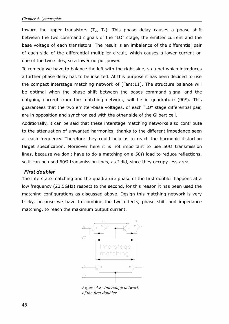
Chapter 4: Quadrupler
toward the upper transistors (T2, T4). This phase delay causes a phase shift
between the two command signals of the “LO” stage, the emitter current and the
base voltage of each transistors. The result is an imbalance of the differential pair
of each side of the differential multiplier circuit, which causes a lower current on
one of the two sides, so a lower output power.
To remedy we have to balance the left with the right side, so a net which introduces
a further phase delay has to be inserted. At this purpose it has been decided to use
the compact interstage matching network of [Fant:11]. The structure balance will
be optimal when the phase shift between the bases command signal and the
outgoing current from the matching network, will be in quadrature (90°). This
guarantees that the two emitter-base voltages, of each “LO” stage differential pair,
are in opposition and synchronized with the other side of the Gilbert cell.
Additionally, it can be said that these interstage matching networks also contribute
to the attenuation of unwanted harmonics, thanks to the different impedance seen
at each frequency. Therefore they could help us to reach the harmonic distortion
target specification. Moreover here it is not important to use 50Ω transmission
lines, because we don't have to do a matching on a 50Ω load to reduce reflections,
so it can be used 60Ω transmission lines, as I did, since they occupy less area.
First doublerThe interstate matching and the quadrature phase of the first doubler happens at a
low frequency (23.5GHz) respect to the second, for this reason it has been used the
matching configurations as discussed above. Design this matching network is very
tricky, because we have to combine the two effects, phase shift and impedance
matching, to reach the maximum output current.
48
Figure 4.8: Interstage network of the first doubler
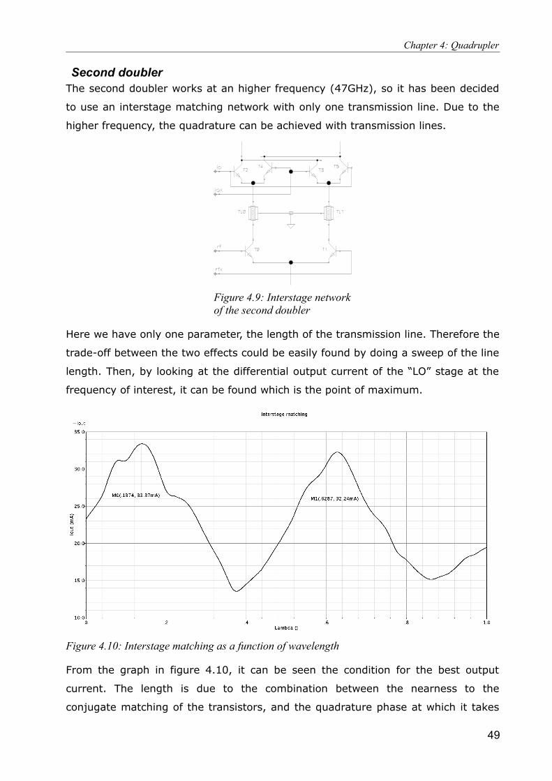
Chapter 4: Quadrupler
Second doublerThe second doubler works at an higher frequency (47GHz), so it has been decided
to use an interstage matching network with only one transmission line. Due to the
higher frequency, the quadrature can be achieved with transmission lines.
Here we have only one parameter, the length of the transmission line. Therefore the
trade-off between the two effects could be easily found by doing a sweep of the line
length. Then, by looking at the differential output current of the “LO” stage at the
frequency of interest, it can be found which is the point of maximum.
From the graph in figure 4.10, it can be seen the condition for the best output
current. The length is due to the combination between the nearness to the
conjugate matching of the transistors, and the quadrature phase at which it takes
49
Figure 4.10: Interstage matching as a function of wavelength
Figure 4.9: Interstage network of the second doubler

Chapter 4: Quadrupler
part also the phase delay introduced by the bipolars. This graph also shows as the
matching is periodic, since the increase the length means to spin on the Smith
chart, without losses every λ2
we are in the same condition. The decreasing of
current, for equivalent length points (every λ2
) is due to the line losses.
4.2.3 Matching networksThe matching networks are typically used to get the maximum power transfer and
minimize the reflections from the load. This is achieved when Z mn=Z L* .
However, in our case, to have the conjugate impedance matching doesn't guarantee
us to get the maximum power (and voltage) on the load. It is true that to have a
conjugate matching means to be able to transfer the maximum output power to the
load, but the gain of the doubler depends on this output impedance. Thus, to get
the maximum voltage (and power) to the output, we have to find the right trade-off
between the increase of the impedance seen from the output of the Gilbert cell
( ZQmn in reference to figure 4.11), and the power transferred to the load, through
the matching network.
For increase the output impedance ( ZQmn ), with the intent of enhance the doubler
gain, we can only act on the matching network, because the load is typically setted
up. But, like already said, increasing the impedance seen from the output of the
Gilbert cell through matching networks and toward the load, creates some
reflections. This power reflection decrease the available power (and voltage) at the
output, according to the following rule [Book:2]:
Pout=12 ∣V in∣
2(1−∣ΓQmn∣2) , where ΓQmn=
Z Qmn−Z0
Z Qmn+Z 0
To find the exact output power we should calculate the impedance seen from the
transistor through the matching network and toward the load ( ZQmn ). Than we
have to combine it with the theoretical gain of the Gilbert cell, keeping into account
also the power transfer function of the interstage matching network.
Unfortunately I wasn't able to find a complete and reliable mathematical relation for
the gain of the doubler as function of the variation of the matching network
impedances. So the simulator has been used to get the maximum output power,
starting from the point of the conjugate matching and increasing the impedance
ZQmn up to the best value for the power.
50
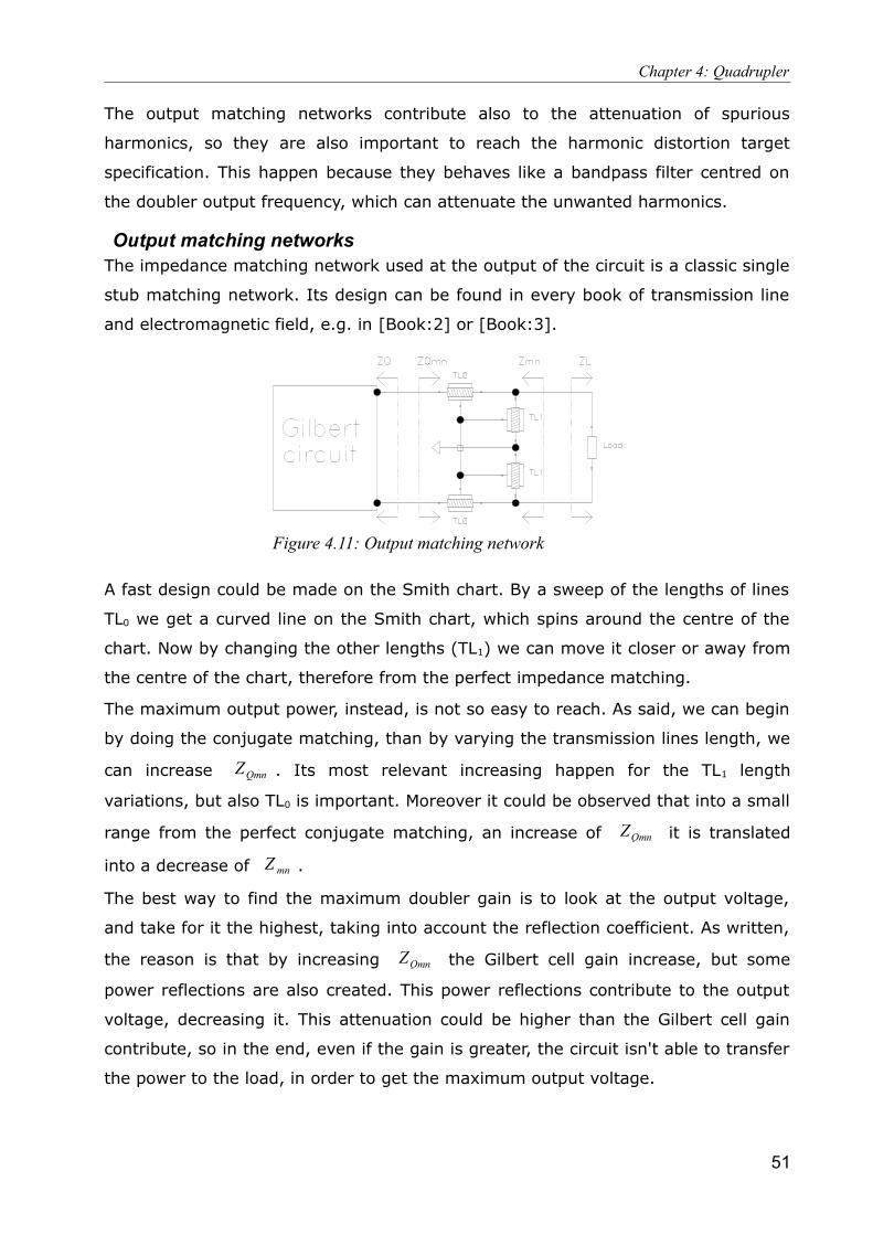
Chapter 4: Quadrupler
The output matching networks contribute also to the attenuation of spurious
harmonics, so they are also important to reach the harmonic distortion target
specification. This happen because they behaves like a bandpass filter centred on
the doubler output frequency, which can attenuate the unwanted harmonics.
Output matching networksThe impedance matching network used at the output of the circuit is a classic single
stub matching network. Its design can be found in every book of transmission line
and electromagnetic field, e.g. in [Book:2] or [Book:3].
A fast design could be made on the Smith chart. By a sweep of the lengths of lines
TL0 we get a curved line on the Smith chart, which spins around the centre of the
chart. Now by changing the other lengths (TL1) we can move it closer or away from
the centre of the chart, therefore from the perfect impedance matching.
The maximum output power, instead, is not so easy to reach. As said, we can begin
by doing the conjugate matching, than by varying the transmission lines length, we
can increase ZQmn . Its most relevant increasing happen for the TL1 length
variations, but also TL0 is important. Moreover it could be observed that into a small
range from the perfect conjugate matching, an increase of ZQmn it is translated
into a decrease of Z mn .
The best way to find the maximum doubler gain is to look at the output voltage,
and take for it the highest, taking into account the reflection coefficient. As written,
the reason is that by increasing ZQmn the Gilbert cell gain increase, but some
power reflections are also created. This power reflections contribute to the output
voltage, decreasing it. This attenuation could be higher than the Gilbert cell gain
contribute, so in the end, even if the gain is greater, the circuit isn't able to transfer
the power to the load, in order to get the maximum output voltage.
51
Figure 4.11: Output matching network
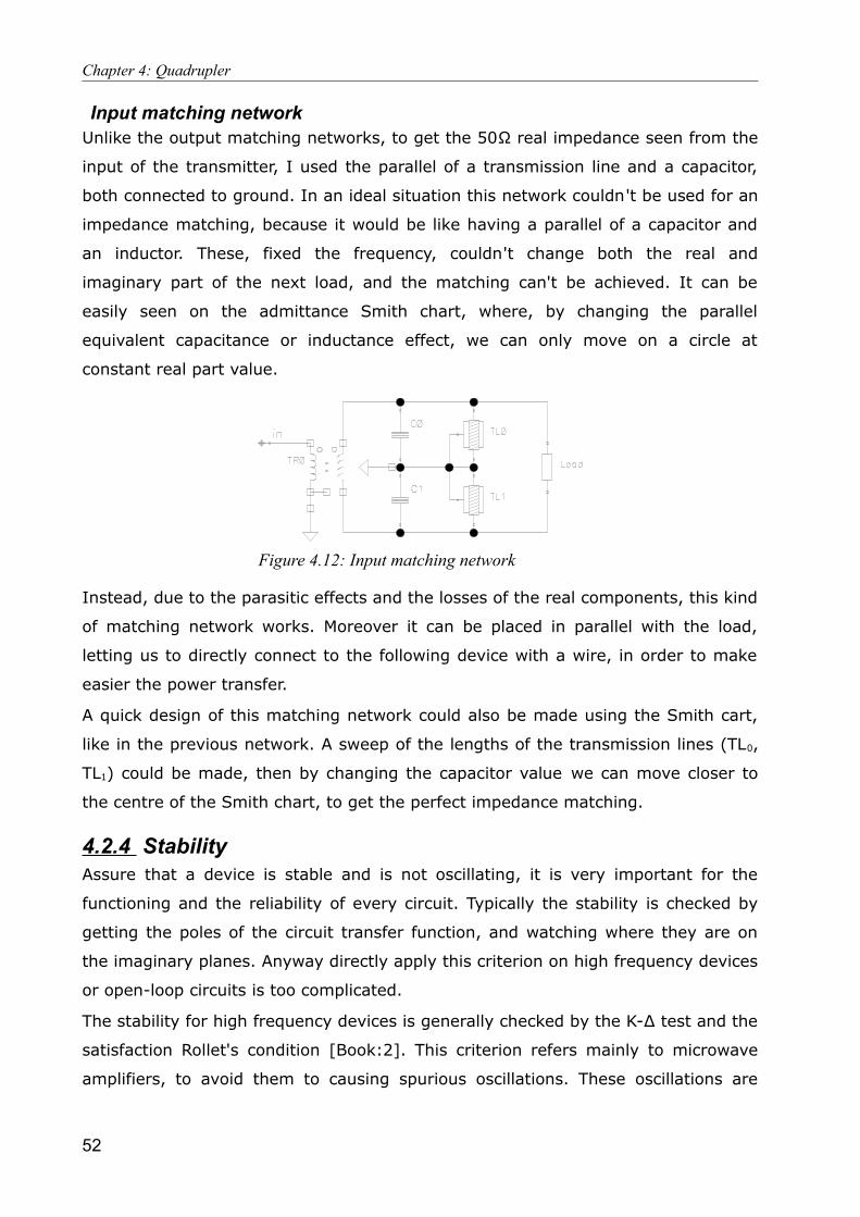
Chapter 4: Quadrupler
Input matching networkUnlike the output matching networks, to get the 50Ω real impedance seen from the
input of the transmitter, I used the parallel of a transmission line and a capacitor,
both connected to ground. In an ideal situation this network couldn't be used for an
impedance matching, because it would be like having a parallel of a capacitor and
an inductor. These, fixed the frequency, couldn't change both the real and
imaginary part of the next load, and the matching can't be achieved. It can be
easily seen on the admittance Smith chart, where, by changing the parallel
equivalent capacitance or inductance effect, we can only move on a circle at
constant real part value.
Instead, due to the parasitic effects and the losses of the real components, this kind
of matching network works. Moreover it can be placed in parallel with the load,
letting us to directly connect to the following device with a wire, in order to make
easier the power transfer.
A quick design of this matching network could also be made using the Smith cart,
like in the previous network. A sweep of the lengths of the transmission lines (TL0,
TL1) could be made, then by changing the capacitor value we can move closer to
the centre of the Smith chart, to get the perfect impedance matching.
4.2.4 StabilityAssure that a device is stable and is not oscillating, it is very important for the
functioning and the reliability of every circuit. Typically the stability is checked by
getting the poles of the circuit transfer function, and watching where they are on
the imaginary planes. Anyway directly apply this criterion on high frequency devices
or open-loop circuits is too complicated.
The stability for high frequency devices is generally checked by the K-∆ test and the
satisfaction Rollet's condition [Book:2]. This criterion refers mainly to microwave
amplifiers, to avoid them to causing spurious oscillations. These oscillations are
52
Figure 4.12: Input matching network
Chapter 4: Quadrupler
possible if either the input or the output impedances, of the device, it has a
negative real part. This implies that one or both the reflection coefficients seen at
the ports are higher than one. A reflection coefficient higher than one means that a
wave greater than the incident is reflected to the source, so a sort of loop is
created, with an increasing on the signal.
If the previous criterion is satisfied, the circuit is considered unconditionally stable,
which means that for all passive source and load impedances it is stable. Otherwise
it is considered conditional stable or potentially unstable, therefore only for a
certain range of passive source and load impedances it will be certainly stable, in
the other situations it could become unstable. For some devices also the transient
response to the step could be helpful to find some potential oscillations or
instabilities. Anyway for more details reference books could be consulted [Book:1],
[Book:2], [Book:3].
K-∆ test and Rollet's condition could also be used for the quadrupler. By this
simulation the quadrupler got some frequencies of potential instability. With the
intent of be more safe, two further capacitors have been added before the output
matching network of the first doubler. This capacitors change the input impedance
to get the unconditional stability, but decrease the output bandwidth and output
power, so a gain redesign has been necessary.
In the particular case of the frequency multiplier, it could be said that the above
small-signal stability criteria cannot be applied to the large signal frequency
multiplication circuitry. However, according to the Barkhausen criterion an
oscillation happens when the feedback signal is at the same frequency of the input
signal with a phase shift of 360° and an amplification >=1 and this single frequency
behaviour can well be detected using the above stability criteria.
53
Chapter 4: Quadrupler
4.2.5 Design result
54
Figure 4.13: Quadrupler final schematic
Chapter 4: Quadrupler
4.3 Layout
55
Figure 4.14: Final release of the quadrupler's layout
Chapter 4: Quadrupler
The layout of the quadrupler has been made following the typical rules for a good
layout. Particular attention, obviously, has been paid for the signal paths, trying to
minimize their length and to avoid the coupling between them. At this purpose also
the distance between two transmission lines has been kept at least of 40μm, if
possible. Moreover crowded ground and VCC planes have been created to avoid
inductive effect for the signal returning current on them, and auto-filling blocking
layers have been placed over the most significant layout regions.
Seen the differential structure of the circuit, the components has been placed in a
completely symmetrical layout, with only some exception for some biasing devices
or paths. This should guarantee an equal behaviour for the two differential signals,
with very similar parasitic elements.
Also heating and current density issues has been taken into account and the width
of each component has been designed in according to the necessity.
The final size of the quadrupler's layout is: 640x340μm2.
4.3.1 Post-layout issuesCompleted the layout it is a must to do the extraction of the parasitic elements,
especially at high frequencies. Through this process we are able to determine the
resistive, capacitive and inductive parasitic elements. They are due to the
placement of the components, to the long paths or to some overlap between wires.
For the quadrupler has been made only the extraction of the capacitive parasitic
elements, because the resistive were negligible and the inductive extraction doesn't
works fine. Moreover only the parasitic capacitance greater than 0.5fF has been
taken into account, the others have been ignored.
This parasitic elements change the behaviour of the device, for this reason they
have been included into the schematics and also simulated, to get how the
behaviour moves.
By doing this simulations with the parasitic element, I saw a high sensitivity to the
inductive elements. For this reason a 2D electromagnetic analysis (with Sonnet) has
been made to get a valuation of the wires inductive behaviour. Only small pieces of
the layout have been analysed with Sonnet, those composed by metal layer or vias
used to connect components along the signal path. The resultant inductive parasitic
elements have been added to the schematic.
Got and placed into the schematic all the relevant parasitic components, a
simulation has been done again, to check if the specifications are still respected and
56
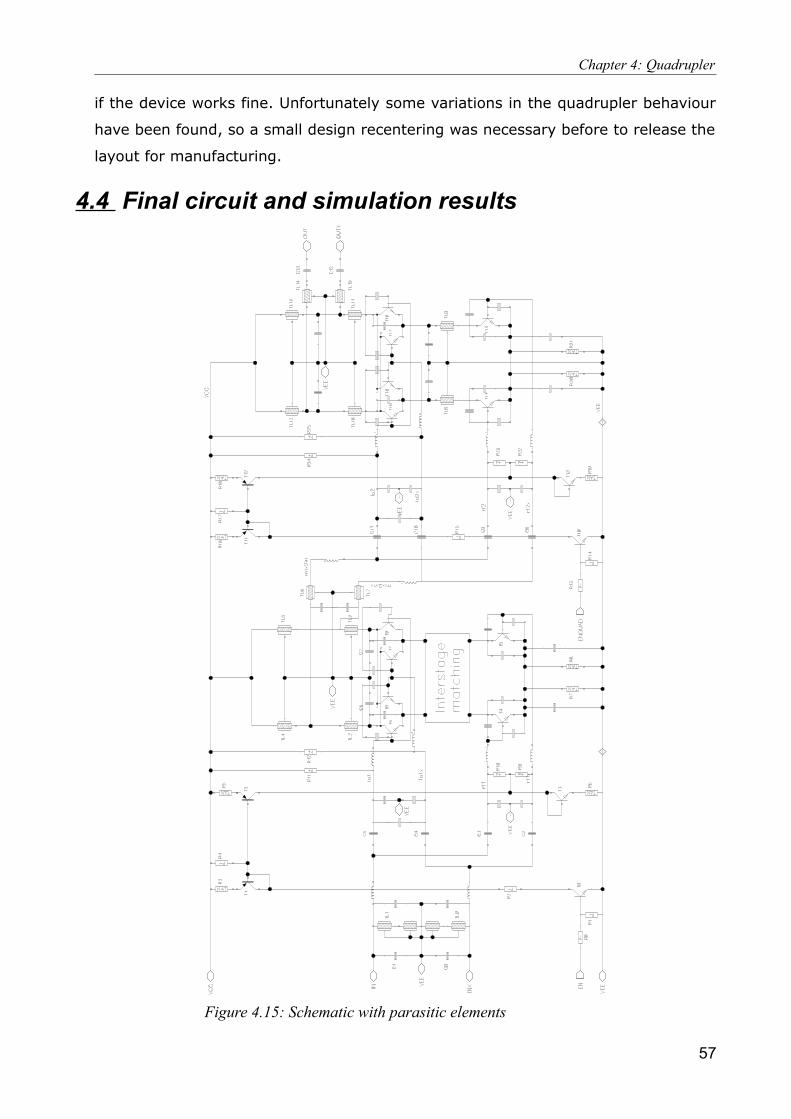
Chapter 4: Quadrupler
if the device works fine. Unfortunately some variations in the quadrupler behaviour
have been found, so a small design recentering was necessary before to release the
layout for manufacturing.
4.4 Final circuit and simulation results
57
Figure 4.15: Schematic with parasitic elements
Chapter 4: Quadrupler
The final version of the quadrupler is shown on figure 4.15, a lots of parasitic
element have been added as explained in the previous section (this components are
represented without labels). The schematic should be near to represent the correct
behaviour of the real device. The final DC current is of roughly 37mA, which
correspond at a power consumption of 122mW.
The quadrupler has been simulated in the schematic showed in figure 4.16, with the
transformer connected at its input and a differential load of 100Ω at the output. The
signal source is a “Port” device with a 50Ω impedance. The source is connected to
one of the transformer pins, while the other is connected to ground. With this
configuration the following simulation results has been reached.
The graph in figure 4.17 shows as the output power target is achieved at every
temperature. Its decreasing is greater at high temperature, while the simulated
conversion gain at 27°C is about 4.4dB.
58
Figure 4.17: Graph of the quadrupler output power vs. temperature
Figure 4.16: Schematic for quadrupler simulation

Chapter 4: Quadrupler
The minimal bandwidth of 2GHz around the central output frequency of 94GHz is
reached. The figure 4.18 shows the bandwidth relative to the input frequency, so
the x-axis has to be multiplied by 4 to get the output frequency. The result is shown
for different temperatures: 0, 27, 50, 100°C (from the top to the bottom line). The
target specification is always respected.
Also the input reflection coefficient (S11) respects the target specification. The
simulation results of an harmonic balance simulation are shown in figure 4.19, with
a temperature variations of 0, 27, 50, 100°C (from the top to the bottom line). This
graph is not centred on the carrier frequency, because the tuning was made with
the buffer as load, given that it is the real load, and not a 100Ω resistor.
59
Figure 4.18: Graph of the quadrupler output power vs. input frequency and temperature
Figure 4.19: Graph of the input reflection coefficient vs. input frequency and temperature
Chapter 4: Quadrupler
The output reflection coefficient (S22), instead, has not been shown since it hasn't
any target specification. At the output of the quadrupler it has been maximized the
power, without any interest for the reflection coefficient.
The graphs in figures 4.20 and 4.21 show the output spectrum at two different
temperatures (27°C and 100°C).
In both the situations the harmonic distortion of -20dBc, for each harmonic, is near.
For the quadrupler there isn't a hard harmonic distortion specification, because only
at the chip output it has to be respected. Anyway here we have to be sure that it
isn't too high, otherwise we couldn't be able to decrease it in following circuits.
60
Figure 4.20: Output spectrum at 27°C
Figure 4.21: Output spectrum at 100°C

Chapter 4: Quadrupler
It is also useful to have a look at the transfer function of the device, which is shown
in figure 4.22 with a temperature variation of 0, 27, 50, 100°C (from the top to the
bottom line).
At roughly -10dBm (depending on temperature), the output power begins to
saturate and for more high input power it decrease. The device is optimized for an
input power of 0dBm, which is the source signal power. It can also pointed out that
with a small variation around this input power (0dBm), the output doesn't change
so much.
61
Figure 4.22: Quadrupler transfer function with temperature variation
Figure 4.23: Transient simulation at 27°C

Chapter 4: Quadrupler
Final, a transient simulation is shown in figure 4.23 with a temperature of 27°C.
The red line is the signal at the input of the transformer, the blue one is the output
of the first doubler and the green one indicates the output of the quadrupler. This
simulation shows as, for the quadrupler, a frequency multiplication by four happens.
62
Chapter 5: Buffer
Chapter 5: Buffer
The amplification stage has been divided into two devices: the buffer and the power
amplifiers. This configuration has been decided to get a more easy and reliable
design for the circuit, given that at these high frequencies only roughly 10dB of
gain per stage are feasible in this process.
The buffer is the first device of the transmitter amplification stage. It has been
chosen to give to it the double purpose of increasing the signal power and, at the
same time, to separate the output of the quadrupler from the following circuits,
giving to it a precise and stable load impedance.
Since the target specification of the transmitter output power is 20dBm at 27°C, it
has been decided to split the amplification in equal part between the two stages.
Therefore the buffet has to be able to reach a target output power of 11dBm at
room temperature, instead it has to reach 8dBm at 100°C. To establish the gain, it
has to be taken into account the worst condition, so the highest temperature. As it
has been shown in the previous chapter, the quadrupler provides a high
temperature output power of 1.2dBm, so the buffer gain should to be roughly 7dB.
Both the input and the output have to ensure a reflection coefficient lower than
-10dB, on an impedance that has been setted to 100Ω differential. This was
decided to guarantee the behaviour of the buffer, that is to separate different
devices on the same chip, allowing a more extreme design for the other devices. As
it will be shown, set these conditions it has the downside to decrease the available
voltage at the input of the transistors, so it requests more gain for the cascode
configuration.
63
Figure 5.1: Buffer schematic symbol
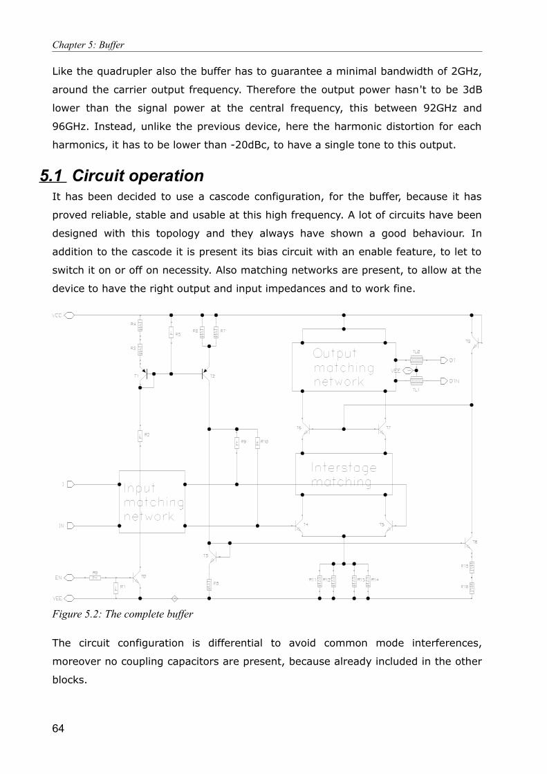
Chapter 5: Buffer
Like the quadrupler also the buffer has to guarantee a minimal bandwidth of 2GHz,
around the carrier output frequency. Therefore the output power hasn't to be 3dB
lower than the signal power at the central frequency, this between 92GHz and
96GHz. Instead, unlike the previous device, here the harmonic distortion for each
harmonics, it has to be lower than -20dBc, to have a single tone to this output.
5.1 Circuit operationIt has been decided to use a cascode configuration, for the buffer, because it has
proved reliable, stable and usable at this high frequency. A lot of circuits have been
designed with this topology and they always have shown a good behaviour. In
addition to the cascode it is present its bias circuit with an enable feature, to let to
switch it on or off on necessity. Also matching networks are present, to allow at the
device to have the right output and input impedances and to work fine.
The circuit configuration is differential to avoid common mode interferences,
moreover no coupling capacitors are present, because already included in the other
blocks.
64
Figure 5.2: The complete buffer
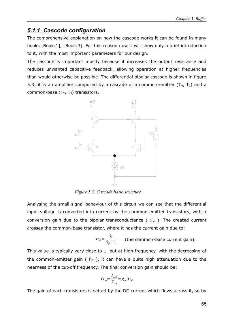
Chapter 5: Buffer
5.1.1 Cascode configurationThe comprehensive explanation on how the cascode works it can be found in many
books [Book:1], [Book:3]. For this reason now it will show only a brief introduction
to it, with the most important parameters for our design.
The cascode is important mostly because it increases the output resistance and
reduces unwanted capacitive feedback, allowing operation at higher frequencies
than would otherwise be possible. The differential bipolar cascode is shown in figure
5.3; it is an amplifier composed by a cascade of a common-emitter (T0, T1) and a
common-base (T2, T3) transistors.
Analysing the small-signal behaviour of this circuit we can see that the differential
input voltage is converted into current by the common-emitter transistors, with a
conversion gain due to the bipolar transconductance ( g m ). The created current
crosses the common-base transistor, where it has the current gain due to:
αF=βF
βF+1 (the common-base current gain).
This value is typically very close to 1, but at high frequency, with the decreasing of
the common-emitter gain ( βF ), it can have a quite high attenuation due to the
nearness of the cut-off frequency. The final conversion gain should be:
Gm=I out
V in=g m⋅αF
The gain of each transistors is setted by the DC current which flows across it, so by
65
Figure 5.3: Cascode basic structure
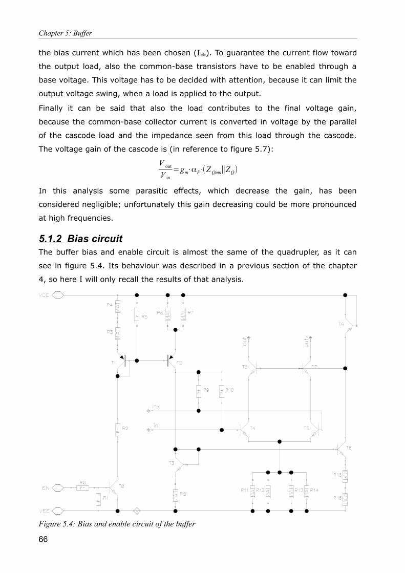
Chapter 5: Buffer
the bias current which has been chosen (IEE). To guarantee the current flow toward
the output load, also the common-base transistors have to be enabled through a
base voltage. This voltage has to be decided with attention, because it can limit the
output voltage swing, when a load is applied to the output.
Finally it can be said that also the load contributes to the final voltage gain,
because the common-base collector current is converted in voltage by the parallel
of the cascode load and the impedance seen from this load through the cascode.
The voltage gain of the cascode is (in reference to figure 5.7):
V out
V in=gm⋅αF⋅(Z Qmn∥ZQ)
In this analysis some parasitic effects, which decrease the gain, has been
considered negligible; unfortunately this gain decreasing could be more pronounced
at high frequencies.
5.1.2 Bias circuitThe buffer bias and enable circuit is almost the same of the quadrupler, as it can
see in figure 5.4. Its behaviour was described in a previous section of the chapter
4, so here I will only recall the results of that analysis.
66
Figure 5.4: Bias and enable circuit of the buffer
Chapter 5: Buffer
The current generated by the enable transistor T0 can be calculated through:
I≈(V CC−V BE−V CEsat)
(R2+R3+R4)= 2.25(R2+R3+R4)
Then this current is mirrored and multiplied by the PNP mirror, which increase the
current of a factor 4, due to resistors and transistor relations ( R3=R4=R6=R7 and
W E (T 2)=4⋅W E(T 1) ). To establish the right bias current into the cascode bipolars, it
has to be seted the NPN mirror composed by T3, T4 and T5, as explained for the
quadrupler.
The only difference between this bias circuit and that one of the quadrupler is the
presence of a further mirror (T3, T8) and one bipolar (T9), which acts as diode. This
configuration is needed to create a biasing voltage for the common-base
transistors. This voltage can be calculated through V BB=V CC−V BE(T 9)=3.3−V BE(T 9)
and slightly varied by the collector current of T9, so through the design of the NPN
current mirror composed by T3 and T8.
This configuration is very reliable to supply voltage variations and process
mismatch, given that V BE(T 9) changes slightly with this parameters. This is also the
reason why its bias current is typically low, to preserve the power consumption. On
the other hand, there is no possibility to set VBB at will. At this purpose other
configurations could be used, for example with some resistors instead of the bipolar
transistor diode connected (T9).
5.2 Design to 94GHzThe design of the buffer is easier compared to the quadrupler, even if also here
there is an high operative frequency, which raise the contributions of the parasitic
elements. Like for quadrupler, the behaviours of the parasitic elements has been
taken into account and it has been tried to describe also the reflection effects.
For a more reliable design already from the beginning, parasitic capacitors from a
similar buffer have been placed around the transistors, in order to prevent a too
great redesign after the post-layout parasitic extraction.
The design requested some iterations, because the target specifications almost
depend on the same components. It started with the choice of the input matching
network and its components value, followed by the establishing of the cascode gain
and its output matching network. Then the output matching network has been
varied to find the optimum trade-off between the reflection coefficient and the
67
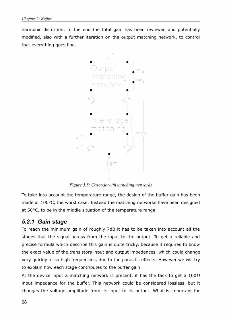
Chapter 5: Buffer
harmonic distortion. In the end the total gain has been reviewed and potentially
modified, also with a further iteration on the output matching network, to control
that everything goes fine.
To take into account the temperature range, the design of the buffer gain has been
made at 100°C, the worst case. Instead the matching networks have been designed
at 50°C, to be in the middle situation of the temperature range.
5.2.1 Gain stageTo reach the minimum gain of roughly 7dB it has to be taken into account all the
stages that the signal across from the input to the output. To get a reliable and
precise formula which describe this gain is quite tricky, because it requires to know
the exact value of the transistors input and output impedances, which could change
very quickly at so high frequencies, due to the parasitic effects. However we will try
to explain how each stage contributes to the buffer gain.
At the device input a matching network is present, it has the task to get a 100Ω
input impedance for the buffer. This network could be considered lossless, but it
changes the voltage amplitude from its input to its output. What is important for
68
Figure 5.5: Cascode with matching networks
Chapter 5: Buffer
the gain is the differential voltage delivered at the bases of the transistors, since
this emitter-base voltage generates the signal current in the cascode. Therefore to
maximize the gain through the input matching network, we have to improve the
voltage transfer function, so the voltage at the bases. Unfortunately this is not
possible at the same time of the 100Ω input impedance matching, so a trade-off
between these two parameters is needed.
The decreasing of voltage happens because at such high frequencies the input
capacitor of the bipolar ( Cπ ) becomes a low impedance load, lower than the 50Ω
seen at the input of the matching network (AC single-ended input impedance). If
this network is lossless, the input and the output power are the same:
P in=∣V in2
50 ∣=∣V out2
Z Qin∣=Pout , with ZQin<50Ω
if the single-ended impedance seen from the base of the transistor is lower than
50Ω, that means that also the voltage will be lower than the input one, and it will
depend on the transistor impedance value. Hence the input matching network
introduces an attenuation in the buffer gain.
The second contribute to the gain is due to the cascode. As shown in a previous
section of this chapter, the theoretical gain depends on the transconductance of the
common-emitter and on the common-base current gain:
Gm=I out
V in=g m⋅αF
Here it has to be taken into account also the attenuation due to the reflection
between the common-emitter and the common-base, which the interstage
matching networks try to remedy. Evaluate with precision this attenuation is
difficult, but it will show in the next section how to proceed to maximize the
transferred current.
Finally, the current coming out from the common-base stage is converted into
voltage by the output matching networks and the cascode output impedance (seen
through the cascode). Given that this cascode impedance is fixed ( ZQ in reference
to figure 5.7), this voltage depends only on the impedance seen from the
transistors through the output matching network toward the following stage ( ZQmn
in reference to figure 5.7). After the conversion, this voltage crosses the matching
network and it could be subjected to reflections due to the not impedance matching
with the load, that could create further attenuations.
69
Chapter 5: Buffer
Increase this impedance ( ZQmn ) to improve the voltage gain, it could be a contrast
with other target specifications. In fact the output matching network has also to be
designed to guarantee the 100Ω output impedance matching for the buffer, and the
attenuation of the spurious harmonics. Therefore a trade-off between this target
specification is required; its explanation will be made in a following section.
5.2.2 Interstage matchingThe interstage matching is a matching network placed between the common-
emitter and the common-base bipolar transistors of the cascode. This networks has
the purpose to reduce the reflections due to the interconnections between the
cascode upper and lower stages (between the emitter and the collector), and it can
also be used to increase the cascode output impedance. Unlike the quadrupler, the
differential structure of the buffer results balanced (left compared to right side),
this is the reason why the quadrature phase tuning, used for the quadrupler, here it
is not necessary.
As for the Gilbert cell, to put here a too complicate network could be
counterproductive for the total gain of the device, due to the losses. For this reason
also here has been placed a simply transmission line to connect the bipolars. Given
that there isn't a high degree of design, for the matching, we simply have to vary
the length of the transmission line to find the position where the current transferred
to the common-base is higher. This can be made by a sweep of the length and
looking at the differential current coming out from the common-base collectors at
the frequency of interest.
By reducing the reflections, this network could also act to reduce the amplifications
of the spurious harmonics, to get the harmonic distortion target. However in this
case it hasn't been used for this goal.
5.2.3 Matching networksThe matching networks, in particular the output one, contribute into almost all the
target specifications, for this reason their design needs some iterations to find the
right trade-off among the requested specifications values.
In the buffer the matching networks are principally used to reach the conjugate
matching, to be able to transfer the maximum output power to the following stage.
This happens because it has been decided to guaranteed, for this device, a very
precise input and output impedances, as reference for the connected devices. This
is the reason why there shouldn't be high power reflections in these nets, but also
70

Chapter 5: Buffer
this issue has to be taken in mind.
These networks have been designed at the temperature of 50°C, to be in the
middle of its variation range, and to not have great changes in the reflection
coefficients at the different temperatures.
Input matching networkThe main goal of the input matching network is to do the impedance matching on a
value of 100Ω differential, to reach a reflection coefficient lower than -10dB. To
achieve this result, it has been chosen to use a “mixed” matching networks: a
circuit between the single stub and the lumped elements matching network. The
configuration can be seen in figure 5.6.
It has been used this network because the impedance seen through the transistors
bases could be easily expressed by the parallel of a resistance and a capacitor, with
low values. Looking the matching into the admittance Smith chart, with this
configuration the impedance saw by the quadrupler can be moved from the
capacitive half circle to the inductance, through the length of the transmission line
(TL0). Then, reached the unity circle of the Smith chart, by the parallel capacitor
(C0), the imaginary part of the inductive impedance can be cancelled, to get the
matching.
The design could be easily made by a sweep of the transmission line length, then
by changing the capacitor value, we can move closer to the centre of the Smith
chart. Finally it has to be reminded that this network also contributes to the gain
with an attenuation, which has to be taken into account.
Output matching networkThe output matching network is the most complicated to design, because it
practically controls every target specification. It is composed by two transmission
71
Figure 5.6: Buffer input matching network

Chapter 5: Buffer
lines, which act for a single stub tuning network. Its main goal is the impedance
matching, to transfer the maximum power to the load; but it will be also used to
increase the gain of the buffer, into the limits of a good reflection coefficient.
As already written, the buffer gain depends on the impedance seen from the
transistors collectors, through the output matching network and toward the
following stage ( ZQmn in reference to figure 5.7). Instead the output reflection
coefficient (S22) depends on how close is to the 100Ω the impedance seen from the
load, through the output matching network and toward the transistors collectors (
Z mn in figure 5.7). These two impedances are obviously correlated, given that
they depend on the same components.
By examining the structure of the matching network, it could be observed that into
a small range from the perfect conjugate matching, an increase of ZQmn it is
translated into a decrease of Z mn . This can be explained by looking at the
admittance Smith chart and watching at the impedance movement on it, by also
taking into account the losses. This explain why both a high gain and a good
reflection coefficient can't be reached together.
To find the right trade-off between gain and reflection, we can begin with the design
of the perfect conjugate matching, which means that Z mn=100Ω . After this, by
varying the transmission lines length, we can increase ZQmn up to the limits of the
reflections specification target, due to Z mn . The most considerable changes
happen for the TL1 length variations, but also TL0 is important. By increasing TL1,
ZQmn increases and the gain too, but Z mn decreases and S22 becomes worst.
The best way to maximize the gain is to look at the output voltage, and take for it
the highest, taking into account the reflection coefficient. As written, the reason is
72
Figure 5.7: Buffer output matching network
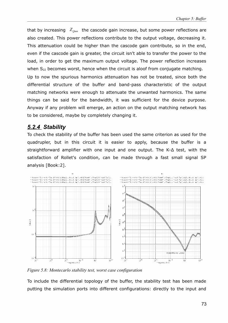
Chapter 5: Buffer
that by increasing ZQmn the cascode gain increase, but some power reflections are
also created. This power reflections contribute to the output voltage, decreasing it.
This attenuation could be higher than the cascode gain contribute, so in the end,
even if the cascode gain is greater, the circuit isn't able to transfer the power to the
load, in order to get the maximum output voltage. The power reflection increases
when S22 becomes worst, hence when the circuit is aloof from conjugate matching.
Up to now the spurious harmonics attenuation has not be treated, since both the
differential structure of the buffer and band-pass characteristic of the output
matching networks were enough to attenuate the unwanted harmonics. The same
things can be said for the bandwidth, it was sufficient for the device purpose.
Anyway if any problem will emerge, an action on the output matching network has
to be considered, maybe by completely changing it.
5.2.4 StabilityTo check the stability of the buffer has been used the same criterion as used for the
quadrupler, but in this circuit it is easier to apply, because the buffer is a
straightforward amplifier with one input and one output. The K-Δ test, with the
satisfaction of Rollet's condition, can be made through a fast small signal SP
analysis [Book:2].
To include the differential topology of the buffer, the stability test has been made
putting the simulation ports into different configurations: directly to the input and
73
Figure 5.8: Montecarlo stability test, worst case configuration
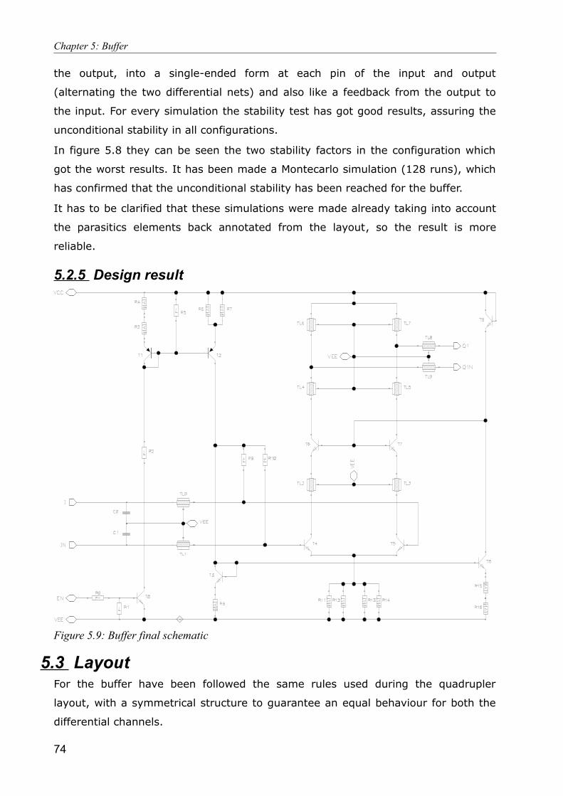
Chapter 5: Buffer
the output, into a single-ended form at each pin of the input and output
(alternating the two differential nets) and also like a feedback from the output to
the input. For every simulation the stability test has got good results, assuring the
unconditional stability in all configurations.
In figure 5.8 they can be seen the two stability factors in the configuration which
got the worst results. It has been made a Montecarlo simulation (128 runs), which
has confirmed that the unconditional stability has been reached for the buffer.
It has to be clarified that these simulations were made already taking into account
the parasitics elements back annotated from the layout, so the result is more
reliable.
5.2.5 Design result
5.3 LayoutFor the buffer have been followed the same rules used during the quadrupler
layout, with a symmetrical structure to guarantee an equal behaviour for both the
differential channels.
74
Figure 5.9: Buffer final schematic
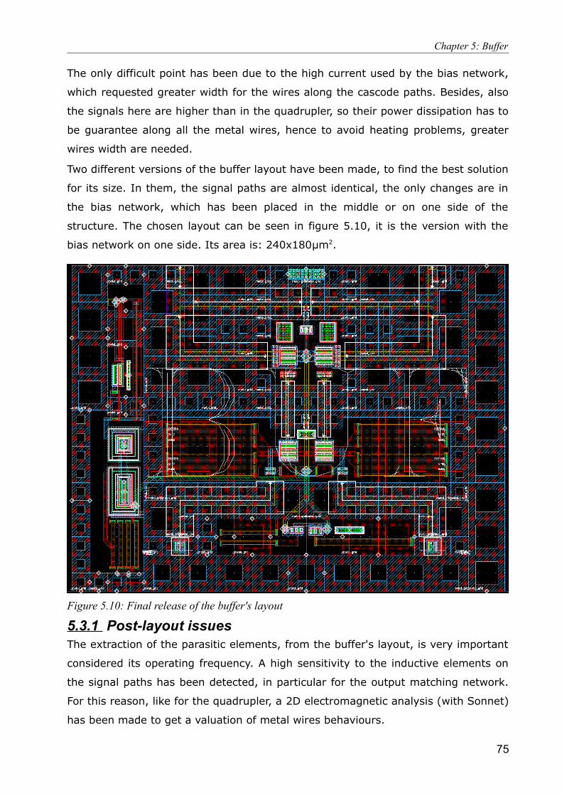
Chapter 5: Buffer
The only difficult point has been due to the high current used by the bias network,
which requested greater width for the wires along the cascode paths. Besides, also
the signals here are higher than in the quadrupler, so their power dissipation has to
be guarantee along all the metal wires, hence to avoid heating problems, greater
wires width are needed.
Two different versions of the buffer layout have been made, to find the best solution
for its size. In them, the signal paths are almost identical, the only changes are in
the bias network, which has been placed in the middle or on one side of the
structure. The chosen layout can be seen in figure 5.10, it is the version with the
bias network on one side. Its area is: 240x180μm2.
5.3.1 Post-layout issuesThe extraction of the parasitic elements, from the buffer's layout, is very important
considered its operating frequency. A high sensitivity to the inductive elements on
the signal paths has been detected, in particular for the output matching network.
For this reason, like for the quadrupler, a 2D electromagnetic analysis (with Sonnet)
has been made to get a valuation of metal wires behaviours.
75
Figure 5.10: Final release of the buffer's layout
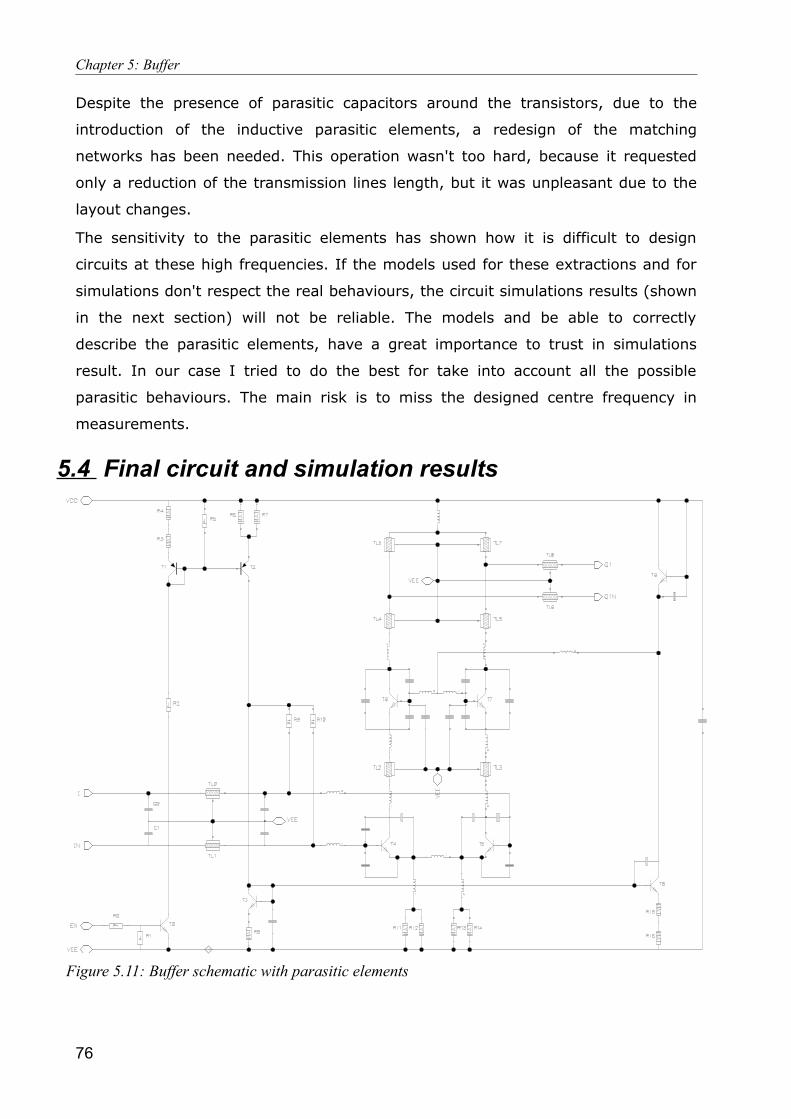
Chapter 5: Buffer
Despite the presence of parasitic capacitors around the transistors, due to the
introduction of the inductive parasitic elements, a redesign of the matching
networks has been needed. This operation wasn't too hard, because it requested
only a reduction of the transmission lines length, but it was unpleasant due to the
layout changes.
The sensitivity to the parasitic elements has shown how it is difficult to design
circuits at these high frequencies. If the models used for these extractions and for
simulations don't respect the real behaviours, the circuit simulations results (shown
in the next section) will not be reliable. The models and be able to correctly
describe the parasitic elements, have a great importance to trust in simulations
result. In our case I tried to do the best for take into account all the possible
parasitic behaviours. The main risk is to miss the designed centre frequency in
measurements.
5.4 Final circuit and simulation results
76
Figure 5.11: Buffer schematic with parasitic elements
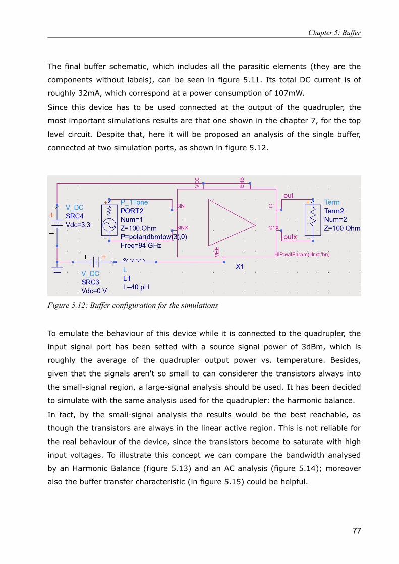
Chapter 5: Buffer
The final buffer schematic, which includes all the parasitic elements (they are the
components without labels), can be seen in figure 5.11. Its total DC current is of
roughly 32mA, which correspond at a power consumption of 107mW.
Since this device has to be used connected at the output of the quadrupler, the
most important simulations results are that one shown in the chapter 7, for the top
level circuit. Despite that, here it will be proposed an analysis of the single buffer,
connected at two simulation ports, as shown in figure 5.12.
To emulate the behaviour of this device while it is connected to the quadrupler, the
input signal port has been setted with a source signal power of 3dBm, which is
roughly the average of the quadrupler output power vs. temperature. Besides,
given that the signals aren't so small to can considerer the transistors always into
the small-signal region, a large-signal analysis should be used. It has been decided
to simulate with the same analysis used for the quadrupler: the harmonic balance.
In fact, by the small-signal analysis the results would be the best reachable, as
though the transistors are always in the linear active region. This is not reliable for
the real behaviour of the device, since the transistors become to saturate with high
input voltages. To illustrate this concept we can compare the bandwidth analysed
by an Harmonic Balance (figure 5.13) and an AC analysis (figure 5.14); moreover
also the buffer transfer characteristic (in figure 5.15) could be helpful.
77
Figure 5.12: Buffer configuration for the simulations
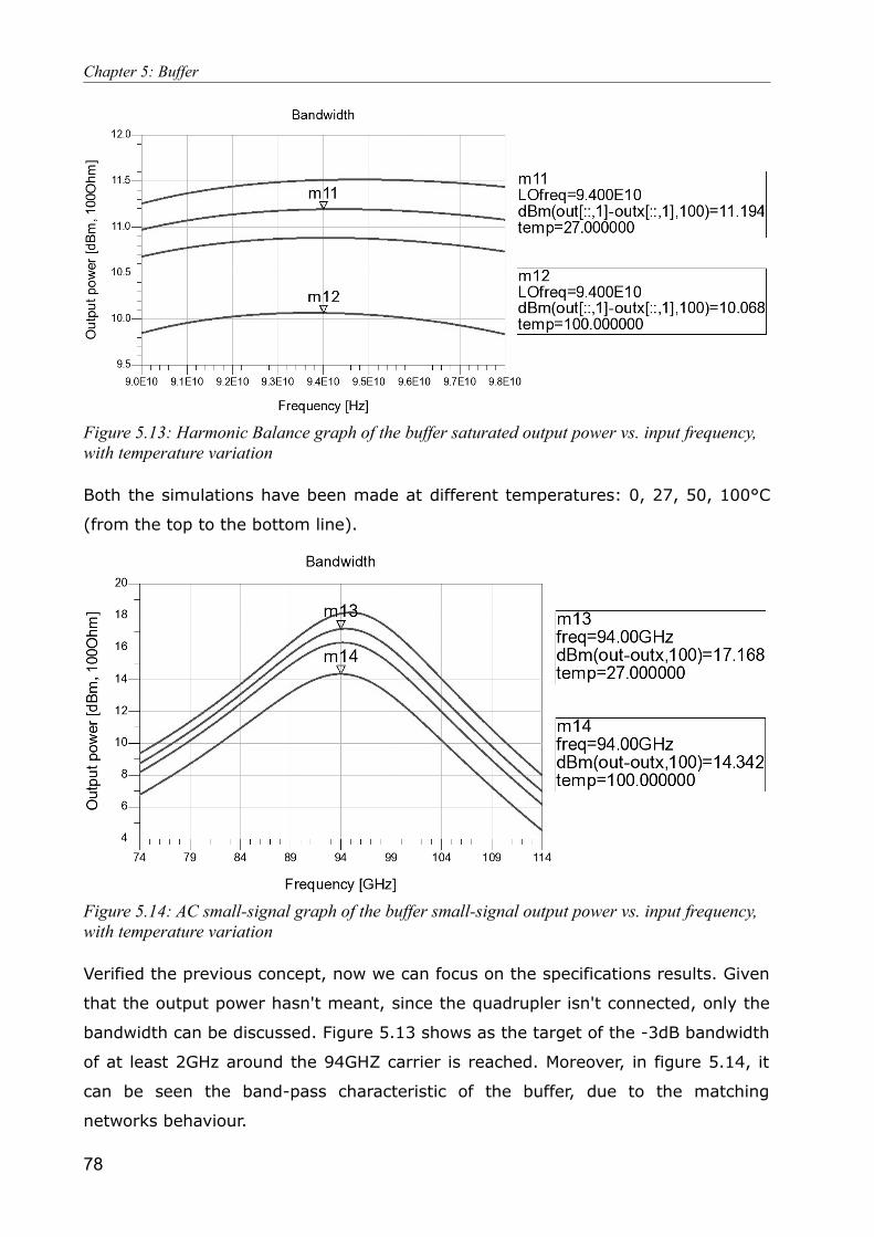
Chapter 5: Buffer
Both the simulations have been made at different temperatures: 0, 27, 50, 100°C
(from the top to the bottom line).
Verified the previous concept, now we can focus on the specifications results. Given
that the output power hasn't meant, since the quadrupler isn't connected, only the
bandwidth can be discussed. Figure 5.13 shows as the target of the -3dB bandwidth
of at least 2GHz around the 94GHZ carrier is reached. Moreover, in figure 5.14, it
can be seen the band-pass characteristic of the buffer, due to the matching
networks behaviour.
78
Figure 5.14: AC small-signal graph of the buffer small-signal output power vs. input frequency, with temperature variation
Figure 5.13: Harmonic Balance graph of the buffer saturated output power vs. input frequency, with temperature variation
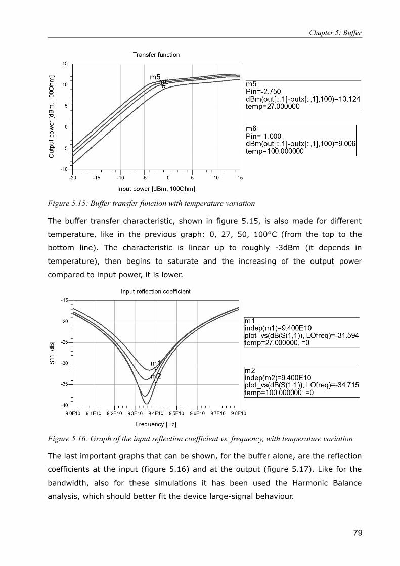
Chapter 5: Buffer
The buffer transfer characteristic, shown in figure 5.15, is also made for different
temperature, like in the previous graph: 0, 27, 50, 100°C (from the top to the
bottom line). The characteristic is linear up to roughly -3dBm (it depends in
temperature), then begins to saturate and the increasing of the output power
compared to input power, it is lower.
The last important graphs that can be shown, for the buffer alone, are the reflection
coefficients at the input (figure 5.16) and at the output (figure 5.17). Like for the
bandwidth, also for these simulations it has been used the Harmonic Balance
analysis, which should better fit the device large-signal behaviour.
79
Figure 5.15: Buffer transfer function with temperature variation
Figure 5.16: Graph of the input reflection coefficient vs. frequency, with temperature variation
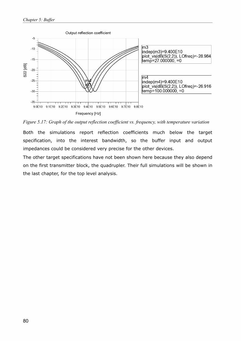
Chapter 5: Buffer
Both the simulations report reflection coefficients much below the target
specification, into the interest bandwidth, so the buffer input and output
impedances could be considered very precise for the other devices.
The other target specifications have not been shown here because they also depend
on the first transmitter block, the quadrupler. Their full simulations will be shown in
the last chapter, for the top level analysis.
80
Figure 5.17: Graph of the output reflection coefficient vs. frequency, with temperature variation
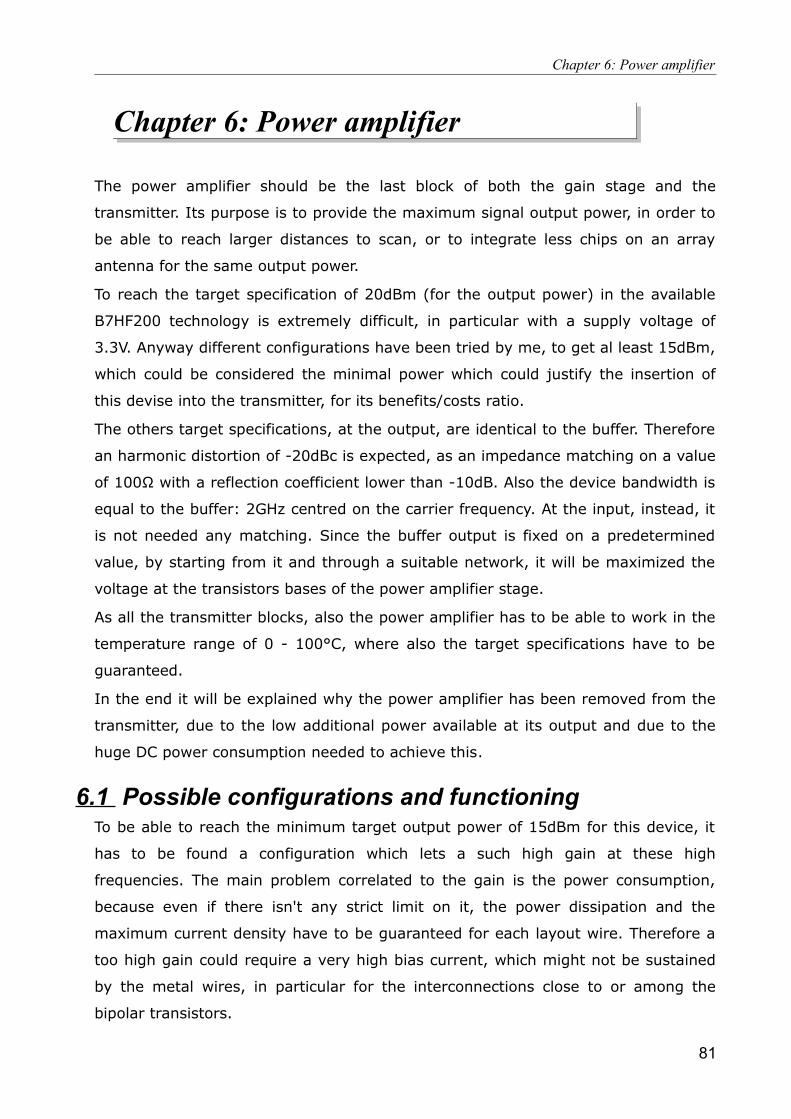
Chapter 6: Power amplifier
Chapter 6: Power amplifier
The power amplifier should be the last block of both the gain stage and the
transmitter. Its purpose is to provide the maximum signal output power, in order to
be able to reach larger distances to scan, or to integrate less chips on an array
antenna for the same output power.
To reach the target specification of 20dBm (for the output power) in the available
B7HF200 technology is extremely difficult, in particular with a supply voltage of
3.3V. Anyway different configurations have been tried by me, to get al least 15dBm,
which could be considered the minimal power which could justify the insertion of
this devise into the transmitter, for its benefits/costs ratio.
The others target specifications, at the output, are identical to the buffer. Therefore
an harmonic distortion of -20dBc is expected, as an impedance matching on a value
of 100Ω with a reflection coefficient lower than -10dB. Also the device bandwidth is
equal to the buffer: 2GHz centred on the carrier frequency. At the input, instead, it
is not needed any matching. Since the buffer output is fixed on a predetermined
value, by starting from it and through a suitable network, it will be maximized the
voltage at the transistors bases of the power amplifier stage.
As all the transmitter blocks, also the power amplifier has to be able to work in the
temperature range of 0 - 100°C, where also the target specifications have to be
guaranteed.
In the end it will be explained why the power amplifier has been removed from the
transmitter, due to the low additional power available at its output and due to the
huge DC power consumption needed to achieve this.
6.1 Possible configurations and functioningTo be able to reach the minimum target output power of 15dBm for this device, it
has to be found a configuration which lets a such high gain at these high
frequencies. The main problem correlated to the gain is the power consumption,
because even if there isn't any strict limit on it, the power dissipation and the
maximum current density have to be guaranteed for each layout wire. Therefore a
too high gain could require a very high bias current, which might not be sustained
by the metal wires, in particular for the interconnections close to or among the
bipolar transistors.
81

Chapter 6: Power amplifier
Also the topology of the circuit is important, because it has to be able to reach an
appropriate output voltage swing, to guarantee the output power. Less transistors
than possible have to be stacked, in order to allow a higher voltage swing; anyhow
in some configurations, as for a cascode, they could be helpful to increase the gain.
During this thesis work some studies have been made and different configurations
have been taken into account [Book:1], with the intent to find a good amplification
behaviour. In the end only two circuits have been designed and simulated, those
whose topology has shown the best target performances, according to the studies
done on them. They will be here introduced and then analysed in the following
sections.
Cascode configurationSince it has got good results for the buffer, it has been decided to design also this
circuit topology for the high output voltage needed from the power amplifier. The
used cascode configuration is identical to the buffer one, with only some little
changes on the bias network. The exceptions are two resistors, one in place of a
diode connected transistor and one into a mirror network.
Emitter follower plus cascodeDue to the high gain required from the power amplifier, it has been tried also a
configuration used for another working device: an automotive amplifier which is
able to reach 20dBm at the frequency of 77GHz, with a supply voltage of 5.5V.
This differential configuration can been seen in figure 6.1 and it is made of an
emitter follower stage, followed by a cascode. The cascode works as in the buffer,
with a bias current which determine the amplification of the signal, together with
the output matching network. Instead, the emitter follower has been added before
the cascode to try to further increase the gain.
This emitter follower is based on a common-collector bipolar, whose collector is
directly connected to the supply voltage, while the emitter is connected the the
cascode stage [Book:1]. To select the right transconductance, the common-
collector transistor is polarized through a bias current which is generated by an
appropriate network connected to its emitter. The negative aspect of this stage is
due to the lower supply voltage used for the transceiver, compared to that one of
the starting circuit, which has necessitated a slight change of the bias network.
With the new bias network the signal current produced by the transistors doesn't
see a high output impedance and so it doesn't receive an adequate amplifications,
with results lower than expected.
82
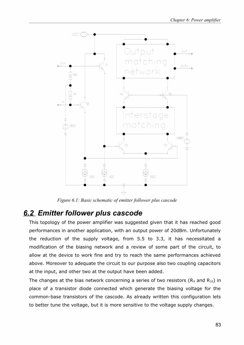
Chapter 6: Power amplifier
6.2 Emitter follower plus cascodeThis topology of the power amplifier was suggested given that it has reached good
performances in another application, with an output power of 20dBm. Unfortunately
the reduction of the supply voltage, from 5.5 to 3.3, it has necessitated a
modification of the biasing network and a review of some part of the circuit, to
allow at the device to work fine and try to reach the same performances achieved
above. Moreover to adequate the circuit to our purpose also two coupling capacitors
at the input, and other two at the output have been added.
The changes at the bias network concerning a series of two resistors (R9 and R10) in
place of a transistor diode connected which generate the biasing voltage for the
common-base transistors of the cascode. As already written this configuration lets
to better tune the voltage, but it is more sensitive to the voltage supply changes.
83
Figure 6.1: Basic schematic of emitter follower plus cascode
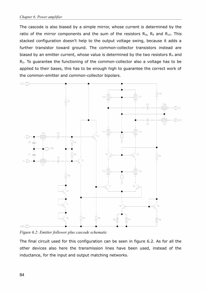
Chapter 6: Power amplifier
The cascode is also biased by a simple mirror, whose current is determined by the
ratio of the mirror components and the sum of the resistors R8, R9 and R10. This
stacked configuration doesn't help to the output voltage swing, because it adds a
further transistor toward ground. The common-collector transistors instead are
biased by an emitter current, whose value is determined by the two resistors R4 and
R5. To guarantee the functioning of the common-collector also a voltage has to be
applied to their bases, this has to be enough high to guarantee the correct work of
the common-emitter and common-collector bipolars.
The final circuit used for this configuration can be seen in figure 6.2. As for all the
other devices also here the transmission lines have been used, instead of the
inductance, for the input and output matching networks.
84
Figure 6.2: Emitter follower plus cascode schematic

Chapter 6: Power amplifier
6.2.1 DesignThe main goal of this device is to produce a high output power, so the design of
every stage of this power amplifier has to be made for maximise the signal current
or voltage in every part of the circuit, obviously without exceed in too high bias
currents, hence in power consumption.
The input matching network is not used to make a conjugate matching, but to get
the maximum voltage at the bases of the common-collector transistors. This
voltage depends on the voltage transfer function through the matching network,
due also to the load seen through the common-collector bases. Another effect
which contribute to this voltage is the impedance seen from the input of the device
toward it, because this participates to the gain of the previous device, the buffer. In
this case the two effect are very close and a trade-off between the two effects has
been found near the conjugate matching.
The voltage gain of the emitter follower depends on the transconductance of the
bipolar, so from its bias current, and on the total impedance seen at the emitter of
the common-collector. This impedance can't be decided according to the desired
gain, because the transistors T3, T4, T7, T8 (in reference to figure 6.2) are designed
according to the transconductance value required, while the resistors R4 and R5 are
used to fix the bias current of the emitter follower stage. Therefore this impedance
can't be used to increase the gain and unfortunately it is also quite low, so it hasn't
allowed high gain for this stage.
After the emitter follower is placed the cascode and its output matching network.
Their behaviours and their contribute to the gain have been well explained for the
buffer in the previous chapter, so here it will be only reminded that to get the
maximum output voltage a trade-off between the gain and the output reflection
coefficient has to be found for the output matching network.
6.2.2 Simulation resultsBefore to start the layout, some simulations on the circuit have been made, to see
which could be the results reached from it and if it is opportune to insert this device
into the transmitter. To analyse the circuit it has been connected in cascade to the
quadrupler and to the buffer, to see the real behaviour in the transmitter.
The simulation graphs of the output power for each transmitter stage vs. the
temperature are shown in figure 6.3. The output of the power amplifier seems to be
acceptable, but it has to be taken into account that the analysed circuit didn't
85
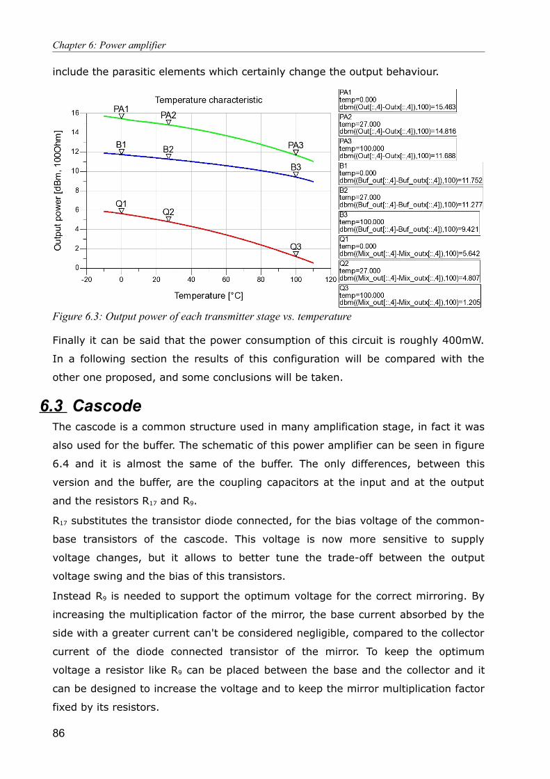
Chapter 6: Power amplifier
include the parasitic elements which certainly change the output behaviour.
Finally it can be said that the power consumption of this circuit is roughly 400mW.
In a following section the results of this configuration will be compared with the
other one proposed, and some conclusions will be taken.
6.3 CascodeThe cascode is a common structure used in many amplification stage, in fact it was
also used for the buffer. The schematic of this power amplifier can be seen in figure
6.4 and it is almost the same of the buffer. The only differences, between this
version and the buffer, are the coupling capacitors at the input and at the output
and the resistors R17 and R9.
R17 substitutes the transistor diode connected, for the bias voltage of the common-
base transistors of the cascode. This voltage is now more sensitive to supply
voltage changes, but it allows to better tune the trade-off between the output
voltage swing and the bias of this transistors.
Instead R9 is needed to support the optimum voltage for the correct mirroring. By
increasing the multiplication factor of the mirror, the base current absorbed by the
side with a greater current can't be considered negligible, compared to the collector
current of the diode connected transistor of the mirror. To keep the optimum
voltage a resistor like R9 can be placed between the base and the collector and it
can be designed to increase the voltage and to keep the mirror multiplication factor
fixed by its resistors.
86
Figure 6.3: Output power of each transmitter stage vs. temperature
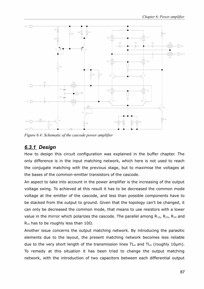
Chapter 6: Power amplifier
6.3.1 DesignHow to design this circuit configuration was explained in the buffer chapter. The
only difference is in the input matching network, which here is not used to reach
the conjugate matching with the previous stage, but to maximise the voltages at
the bases of the common-emitter transistors of the cascode.
An aspect to take into account in the power amplifier is the increasing of the output
voltage swing. To achieved at this result it has to be decreased the common mode
voltage at the emitter of the cascode, and less than possible components have to
be stacked from the output to ground. Given that the topology can't be changed, it
can only be decreased the common mode, that means to use resistors with a lower
value in the mirror which polarizes the cascode. The parallel among R12, R13, R14 and
R15 has to be roughly less than 10Ω.
Another issue concerns the output matching network. By introducing the parasitic
elements due to the layout, the present matching network becomes less reliable
due to the very short length of the transmission lines TL4 and TL5 (roughly 10μm).
To remedy at this situation it has been tried to change the output matching
network, with the introduction of two capacitors between each differential output
87
Figure 6.4: Schematic of the cascode power amplifier
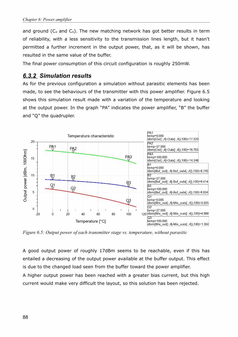
Chapter 6: Power amplifier
and ground (C4 and C5). The new matching network has got better results in term
of reliability, with a less sensitivity to the transmission lines length, but it hasn't
permitted a further increment in the output power, that, as it will be shown, has
resulted in the same value of the buffer.
The final power consumption of this circuit configuration is roughly 250mW.
6.3.2 Simulation resultsAs for the previous configuration a simulation without parasitic elements has been
made, to see the behaviours of the transmitter with this power amplifier. Figure 6.5
shows this simulation result made with a variation of the temperature and looking
at the output power. In the graph “PA” indicates the power amplifier, “B” the buffer
and “Q” the quadrupler.
A good output power of roughly 17dBm seems to be reachable, even if this has
entailed a decreasing of the output power available at the buffer output. This effect
is due to the changed load seen from the buffer toward the power amplifier.
A higher output power has been reached with a greater bias current, but this high
current would make very difficult the layout, so this solution has been rejected.
88
Figure 6.5: Output power of each transmitter stage vs. temperature, without parasitic
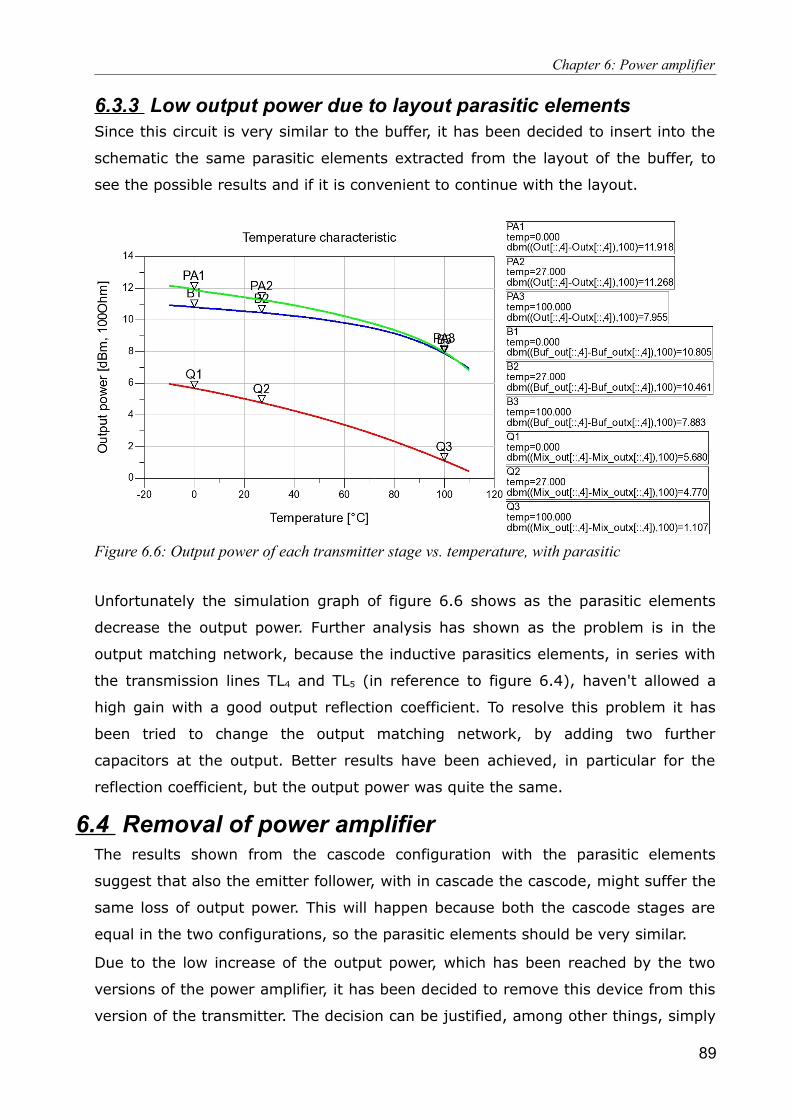
Chapter 6: Power amplifier
6.3.3 Low output power due to layout parasitic elementsSince this circuit is very similar to the buffer, it has been decided to insert into the
schematic the same parasitic elements extracted from the layout of the buffer, to
see the possible results and if it is convenient to continue with the layout.
Unfortunately the simulation graph of figure 6.6 shows as the parasitic elements
decrease the output power. Further analysis has shown as the problem is in the
output matching network, because the inductive parasitics elements, in series with
the transmission lines TL4 and TL5 (in reference to figure 6.4), haven't allowed a
high gain with a good output reflection coefficient. To resolve this problem it has
been tried to change the output matching network, by adding two further
capacitors at the output. Better results have been achieved, in particular for the
reflection coefficient, but the output power was quite the same.
6.4 Removal of power amplifierThe results shown from the cascode configuration with the parasitic elements
suggest that also the emitter follower, with in cascade the cascode, might suffer the
same loss of output power. This will happen because both the cascode stages are
equal in the two configurations, so the parasitic elements should be very similar.
Due to the low increase of the output power, which has been reached by the two
versions of the power amplifier, it has been decided to remove this device from this
version of the transmitter. The decision can be justified, among other things, simply
89
Figure 6.6: Output power of each transmitter stage vs. temperature, with parasitic
Chapter 6: Power amplifier
comparing the power consumption: the DC power of each power amplifier is greater
than the rest of the transmitter, for a very low output power increasing. Moreover
the actual transmitters on the market provide an output power of roughly 10dBm.
Therefore, in the end it has been decided to deliver a first version of the transmitter
without power amplifier, and to go into more depth for it in a subsequent analysis.
90

Chapter 7: Top level circuit
Chapter 7: Top level circuit
Designed all the devices which have to be placed into the transmitter, and decided
to remove the power amplifier due to its low output power, it is necessary to
connect the devices together and to verify the simulation performances of the
complete circuit.
In addition to the circuits described up to now, it has been decided to insert into the
chip also a temperature sensor and a power detector. They were available as library
and they have been already used in many other projects. The temperature sensor is
obviously necessary to know the internal temperature of the silicon transmitter, and
to control if the measured performances are comparable with the simulated in the
same condition. The power detector is used to check the availability of the power at
the output of the transmitter and to provide a simple production test of the output
signal, seen the difficulty to do measurements on all devices at such high
frequencies.
The circuit has been completed with an ESD protection for each connection toward
the external environment. Also between the supply connections (VCC and ground)
ESD power supply clamps have been placed. Moreover to avoid unwanted
oscillations of the power supply and to increase the stability of the circuit, a grid of
capacitors has been placed between the supply and ground. The interconnections
among the different devices have been made with transmission lines, which
shouldn't vary the signal transfer function between each device, because in order to
avoid this situation an impedance matching had been designed.
Into the top level simulation check some unwanted behaviours have been
discovered, so a slightly redesign has been necessary. In particular the buffer
output matching network has been adapted to the chip output condition, with the
additional load capacitances of the power detector and the pads. These effects
hadn't been taken in account during its design because the power amplifier should
be last output stage. Anyway an optimum buffer redesign has been made and the
performances have been preserved.
7.1 SchematicThe top level schematic of the transmitter can be seen in figure 7.1, all the
elements placed into the layout has been inserted.
91
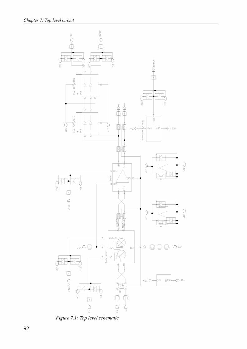
Chapter 7: Top level circuit
92
Figure 7.1: Top level schematic
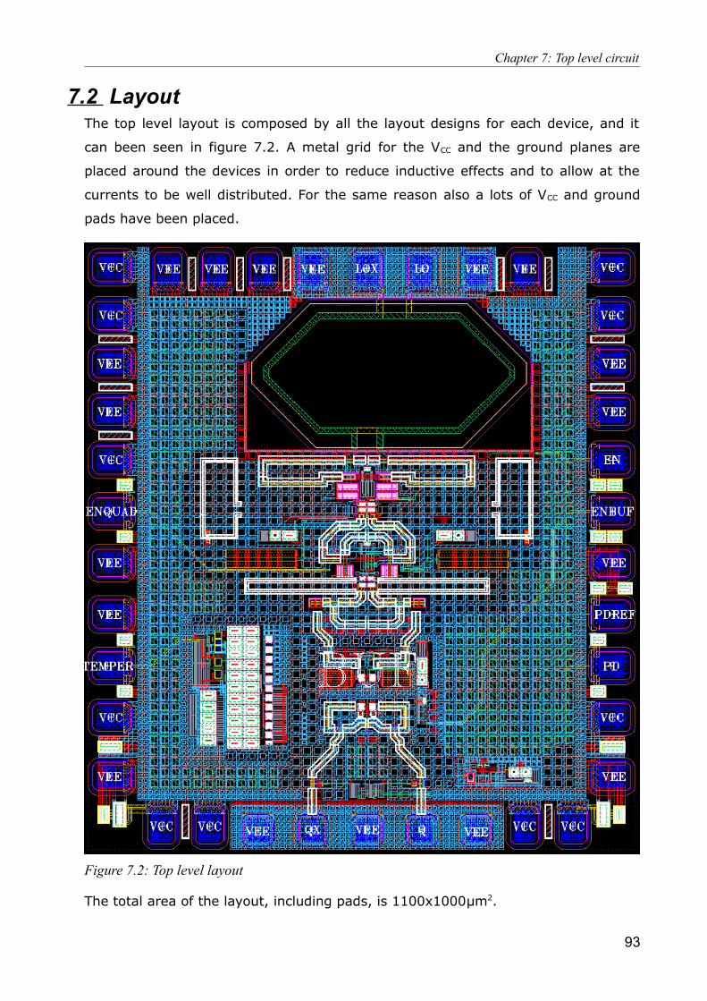
Chapter 7: Top level circuit
7.2 LayoutThe top level layout is composed by all the layout designs for each device, and it
can been seen in figure 7.2. A metal grid for the VCC and the ground planes are
placed around the devices in order to reduce inductive effects and to allow at the
currents to be well distributed. For the same reason also a lots of VCC and ground
pads have been placed.
The total area of the layout, including pads, is 1100x1000μm2.
93
Figure 7.2: Top level layout
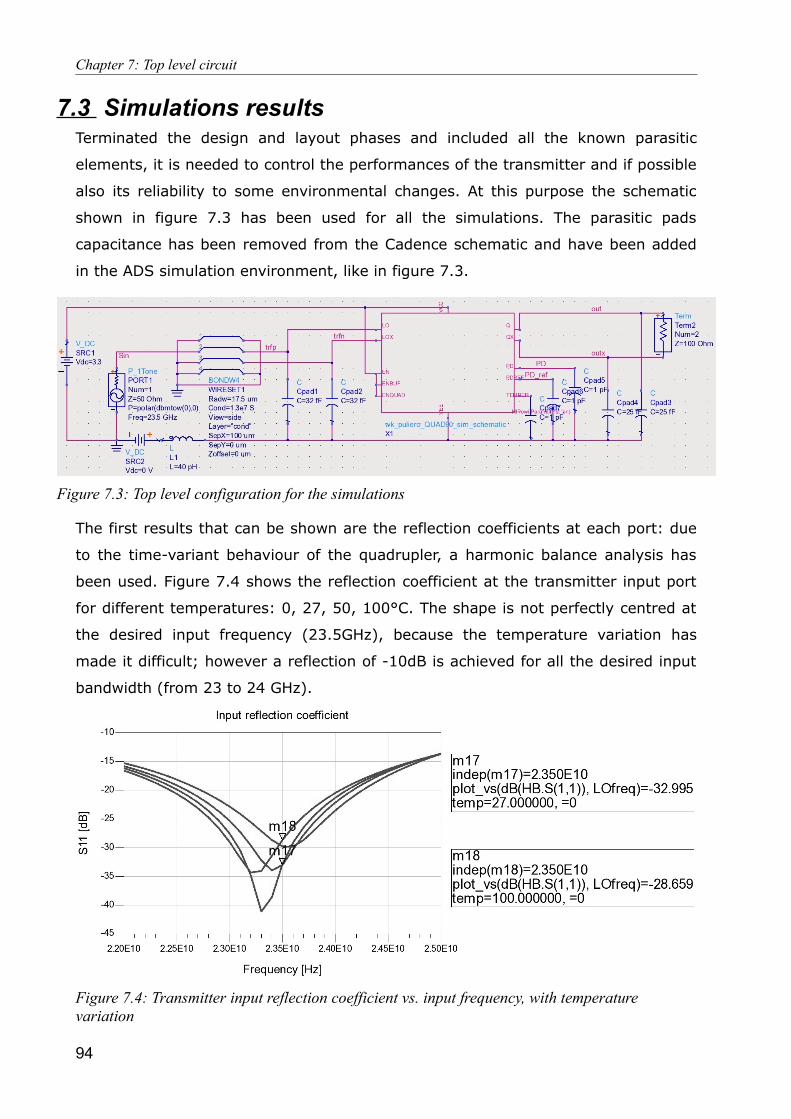
Chapter 7: Top level circuit
7.3 Simulations resultsTerminated the design and layout phases and included all the known parasitic
elements, it is needed to control the performances of the transmitter and if possible
also its reliability to some environmental changes. At this purpose the schematic
shown in figure 7.3 has been used for all the simulations. The parasitic pads
capacitance has been removed from the Cadence schematic and have been added
in the ADS simulation environment, like in figure 7.3.
The first results that can be shown are the reflection coefficients at each port: due
to the time-variant behaviour of the quadrupler, a harmonic balance analysis has
been used. Figure 7.4 shows the reflection coefficient at the transmitter input port
for different temperatures: 0, 27, 50, 100°C. The shape is not perfectly centred at
the desired input frequency (23.5GHz), because the temperature variation has
made it difficult; however a reflection of -10dB is achieved for all the desired input
bandwidth (from 23 to 24 GHz).
94
Figure 7.3: Top level configuration for the simulations
Figure 7.4: Transmitter input reflection coefficient vs. input frequency, with temperature variation
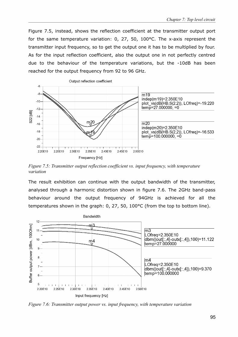
Chapter 7: Top level circuit
Figure 7.5, instead, shows the reflection coefficient at the transmitter output port
for the same temperature variation: 0, 27, 50, 100°C. The x-axis represent the
transmitter input frequency, so to get the output one it has to be multiplied by four.
As for the input reflection coefficient, also the output one in not perfectly centred
due to the behaviour of the temperature variations, but the -10dB has been
reached for the output frequency from 92 to 96 GHz.
The result exhibition can continue with the output bandwidth of the transmitter,
analysed through a harmonic distortion shown in figure 7.6. The 2GHz band-pass
behaviour around the output frequency of 94GHz is achieved for all the
temperatures shown in the graph: 0, 27, 50, 100°C (from the top to bottom line).
95
Figure 7.5: Transmitter output reflection coefficient vs. input frequency, with temperature variation
Figure 7.6: Transmitter output power vs. input frequency, with temperature variation
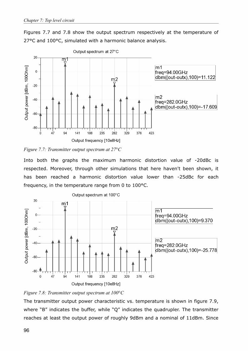
Chapter 7: Top level circuit
Figures 7.7 and 7.8 show the output spectrum respectively at the temperature of
27°C and 100°C, simulated with a harmonic balance analysis.
Into both the graphs the maximum harmonic distortion value of -20dBc is
respected. Moreover, through other simulations that here haven't been shown, it
has been reached a harmonic distortion value lower than -25dBc for each
frequency, in the temperature range from 0 to 100°C.
The transmitter output power characteristic vs. temperature is shown in figure 7.9,
where “B” indicates the buffer, while “Q” indicates the quadrupler. The transmitter
reaches at least the output power of roughly 9dBm and a nominal of 11dBm. Since
96
Figure 7.7: Transmitter output spectrum at 27°C
Figure 7.8: Transmitter output spectrum at 100°C
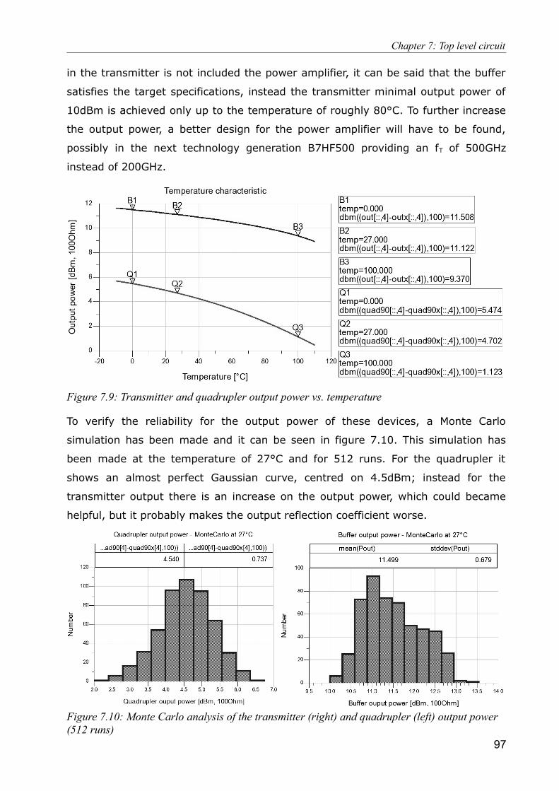
Chapter 7: Top level circuit
in the transmitter is not included the power amplifier, it can be said that the buffer
satisfies the target specifications, instead the transmitter minimal output power of
10dBm is achieved only up to the temperature of roughly 80°C. To further increase
the output power, a better design for the power amplifier will have to be found,
possibly in the next technology generation B7HF500 providing an fT of 500GHz
instead of 200GHz.
To verify the reliability for the output power of these devices, a Monte Carlo
simulation has been made and it can be seen in figure 7.10. This simulation has
been made at the temperature of 27°C and for 512 runs. For the quadrupler it
shows an almost perfect Gaussian curve, centred on 4.5dBm; instead for the
transmitter output there is an increase on the output power, which could became
helpful, but it probably makes the output reflection coefficient worse.
97
Figure 7.9: Transmitter and quadrupler output power vs. temperature
Figure 7.10: Monte Carlo analysis of the transmitter (right) and quadrupler (left) output power (512 runs)
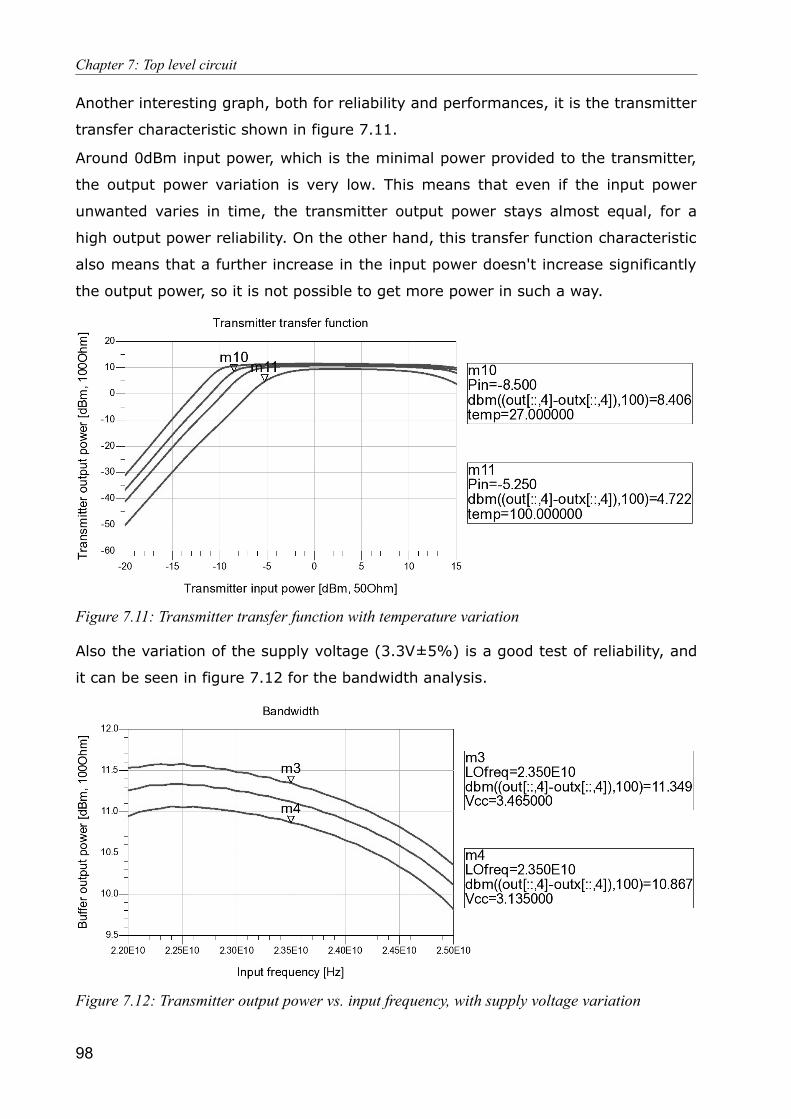
Chapter 7: Top level circuit
Another interesting graph, both for reliability and performances, it is the transmitter
transfer characteristic shown in figure 7.11.
Around 0dBm input power, which is the minimal power provided to the transmitter,
the output power variation is very low. This means that even if the input power
unwanted varies in time, the transmitter output power stays almost equal, for a
high output power reliability. On the other hand, this transfer function characteristic
also means that a further increase in the input power doesn't increase significantly
the output power, so it is not possible to get more power in such a way.
Also the variation of the supply voltage (3.3V±5%) is a good test of reliability, and
it can be seen in figure 7.12 for the bandwidth analysis.
98
Figure 7.11: Transmitter transfer function with temperature variation
Figure 7.12: Transmitter output power vs. input frequency, with supply voltage variation
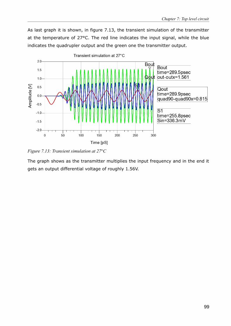
Chapter 7: Top level circuit
As last graph it is shown, in figure 7.13, the transient simulation of the transmitter
at the temperature of 27°C. The red line indicates the input signal, while the blue
indicates the quadrupler output and the green one the transmitter output.
The graph shows as the transmitter multiplies the input frequency and in the end it
gets an output differential voltage of roughly 1.56V.
99
Figure 7.13: Transient simulation at 27°C
Chapter 8: Conclusions
Chapter 8: Conclusions
A transmitter for weather radar applications has been designed, simulated and
layouted. A nominal output power of 11dBm has been reached with a 2GHz
bandwidth around the output central frequency of 94GHz. The input and the output
reflection coefficients are well below the target specification of -10dB, while an
harmonic distortion of -25dBc has been reached for each harmonics. The
temperature operative range is from 0 to 100°C.
The transmitter has a 50Ω single-ended input and a 100Ω differential output. It is
composed by a transformer (which acts as BalUn), a frequency quadrupler and a
buffer. To implement these devices it has been used the Infineon B7HF200 bipolar
technology, with a cut-off frequency of 200GHz for ultra high frequency
applications.
With these encouraging simulation results it has been done a layout for the
transmitter, trying to reduce the parasitics effects with the intent to preserve the
circuit behaviour. In the end the transmitter layout has been sent to the foundry, for
a test chip. Silicon is expected to become available mid of 2011.
100
Bibliography
Bibliography
Books:
[Book:1] ~ “Analysis and design of analog integrated circuits” 4th Ed.; P.R.Gray, P.J.Hurst, S.H.Lewis, R.G.Meyer; 2001.
[Book:2] ~ “Microwave Engineering” 3rd Ed.; David M. Pozar; 2005. [Book:3] ~ “The design of CMOS radio-frequency integrated circuits” 2nd Ed.; Thomas H.
Lee; 2004 [Book:4] ~ “Device electronics for integrated circuits” 3rd Ed.; R.S.Muller, T.I.Kamins; 2003 [Book:5] ~ “Principles of Modern Radar: Basic Principles”;M.A.Richards, J.A.Scheer,
W.A.Holm; 2010. [Book:6] ~ “Radar Handbook” 3rd Ed.; Merrill Skolnik; 2008. [Book:7] ~ “SiGe heterojunction bipolar transistors”; Peter Ashburn; 2003. [Book:8] ~ “Digital integrated circuits” 2nd Ed.; J. Rabaey; 2003.
Thesis:
[Puchner:96] ~ PhD thesis, Helmut Puchner, “Advanced Process Modeling for VLSI Technology”; 1996.
[Fant:11] ~ MSc thesis, Tomaso Fant, “Monolithic millimeter-wave frequency multipliers”; 2011.
[Remund:04] ~ MSc thesis, Craig T. Remund, “Design of CMOS four-quadrant Gilbert cell multiplier circuits in weak and moderate inversion”; 2004.
[Altaf:07] ~ MSc thesis, Amjad Altaf, “Design of millimeter-wave SiGe frequency doubler and output buffer for automotive radar applications”; 2007.
[Hashemi:03] ~ MSc thesis, Hossein Hashemi, “Integrated concurrent multi-band radios and multiple-antenna systems”; 2003.
[Ye:01] ~ MSc thesis, Song Ye, “1 V, 1.9 GHz CM0S Mixers for Wireless Applications”; 2001.
[Upadhyaya:01] ~ MSc thesis, Parag Upadhyaya, “High IIP2 CMOS doubly balanced quadrature sub-harmonic mixer for 5GHz direct conversion receiver”
Papers:
[Tiebout:11] ~ M. Tiebout, H.-D.Wohlmuth, H. Knapp , R. Salerno, M. Druml, J. Kaeferboeck, M. Rest, J.Wuertele, S. S. Ahmed, A. Schiessl, R. Juenemann, “Low power wideband receiver and transmitter chipset for mm-wave imaging in SiGe bipolar technology”; 2011.
[Gilbert:68] ~ B.Gilbert, “A precise four-quadrant multiplier with subnanosecond response”, IEEE J. Solid-State Circuits, Vol. SC-3, pp.365-373, December 1968.
[Boeck:04] ~ J. Boeck, H. Schaefer, K. Aufinger et al, “SiGe Bipolar Technology for Automotive Radar Applications,” in Proc. Bipolar/BiCMOS Circuits and Technology Meeting (BCTM'04), Montreal, Canada, Sept. 2004, pp. 84–87.
[Infineon:06] ~ www.infineon.com, “B7HF200 - 200 GHz SiGe Technology”, 2006.
101

Bibliography
[Knapp:08] ~ Herbert Knapp and Hans-Peter Forstner, “77-GHz Automotive Radar Transceivers in SiGe”; 2008.
[Forstner:08] ~ H. P. Forstner, H. Knapp, H. Jaeger et al, “ A 77GHz 4-Channel Automotive Radar Transceiver in SiGe ,” in RFIC Proceedings. IEEE, June 2008.
[Lachner:07] ~ Rudolf Lachner, “Low Cost SiGe Technology for Automotive Radar Sensors in the 76-81 GHz Band”; 2007.
[Trotta:07] ~ S. Trotta, B. Dehlink, H. Knapp et al, “Design Considerations for Low-Noise, Highly-Linear Millimeter- Wave Mixers in SiGe Bipolar Technology,” in RFIC Proceedings. IEEE, June 2007.
[Dehlink:06] ~ Bernhard Dehlink, Hans-Dieter Wohlmuth, Klaus Aufinger, Franz Weiss and Arpad L. Scholtz “An 80 GHz SiGe Quadrature Receiver Frontend”; 2006.
[Dehlink:05] ~ B. Dehlink et al., “A low-noise amplifier at 77 GHz in SiGe:C bipolar technology” in Compound Semiconductor Integrated Circuit (CSIC) Symposium. Palm Springs, USA: IEEE, Oct – Nov 2005, pp. 287–290.
[Dehlink:06b] ~ B. Dehlink, “A Highly Linear SiGe Double–Balanced Mixer for 77 GHz Automotive Radar Applications”; 2006.
[Appleby:04] ~ Roger Appleby, Rupert N. Anderton, Neil H. Thomson and James W. Jack, "The design of a real-time 94-GHz passive millimetre-wave imager for helicopter operations", Proc. SPIE 5619, 38; 2004.
[Winkler:04] ~ W. Winkler et al., “60 GHz Transceiver Circuits in SiGe:C BiCMOS Technology,” in Proceedings of the 30th European Solid-State Circuits Conference. IEEE, September 2004, pp. 83–86.
[Biondi:06] ~ Tonio Biondi, Angelo Scuderi, Egidio Ragonese and Giuseppe Palmisano, “Analysis and Modeling of Layout Scaling in Silicon Integrated Stacked Transformers”; 2006.
[Scuderi:04] ~ Angelo Scuderi, Tonio Biondi, Egidio Ragonese and Giuseppe Palmisano, “A Lumped Scalable Model for Silicon Integrated Spiral Inductors”; 2004.
[Laskin:08] ~ Ekaterina Laskin, Pascal Chevalier, Alain Chantre, Bernard Sautreuil and Sorin P. Voinigescu, “165-GHz Transceiver in SiGe Technology”; 2008.
[Gan:06] ~ Haitao Gan, S. Simon Wong, “Integrated Transformer Baluns for RF Low Noise and Power Amplifiers”; 2006.
[Moldovan:04] ~ Emilia Moldovan, Serioja Ovidiu Tatu, Tamara Gaman, “A New 94 GHz Collision Avoidance Radar Sensor Using Six-Port Phase Frequency Discriminator”; 2004.
[Mouthaan:97] ~ K. Mouthaan and R. Tinti and M. de Kok and H.C. de Graaff and J.L. Tauritz and J. Slotboom, "Microwave modelling and measurement of the self- and mutual inductance of coupled bondwires," Proceedings of the 1997 Bipolar/BiCMOS Circuits and Technology Meeting, pp.166-169, September 1997.
[Harm:98] ~ A.O. Harm and K. Mouthaan and E. Aziz and M. Versleijen, "Modelling and Simulation of Hybrid RF Circuits Using a Versatile Compact Bondwire Model," Proceedings of the European Microwave Conference, pp. 529-534, Oct. 1998. Amsterdam.
Internet:
[Int:1] ~ Wikipedia (www.wikipedia.org). [Int:2] ~ http://edocs.soco.agilent.com/display/ads2008U1/BONDW1+to+BONDW50+
(Philips-TU+Delft+Bondwires+Model)
102