Embed Size (px)
Citation preview

ýomputer-Aided Design Package for Designers of Digital Optical Computers
Go Annual Report for Grant #N00014-90-J-4018 for Period 5/1/91 - 4/30/92
""E Principal Investigator: Miles Murdocca . -T -1Department of Computer Science
1b0 Rutgers University, Hill Center LE CC • New Brunswick, NJ 08903 ELEC' "
(908) 932-2654 AUGO 5 [email protected]
SMay, 1992A
Summary
*his report covers progress for the period 5/1/91 - 4/30/92 on a jointly sponsored AFOSR/ONRgrant to Rutgers University that supports research in architecture and design of digital opticalcomputers. Progress for this reporting period includes the development of an interactive designtool for digital optical circuits, the development of optical interconnection methods, and aninvestigation into the architectural implications of reconfigurable optical interconnects. Prior to thisreporting period, an emphasis had been placed on the Bell Labs style of digital optical processor, inwhich arrays of optical logic gates are interconnected in free space with regular patterns at the gatelevel. The computer-aided design (CAD) tools and the optical interconnection methods that wehave been developing allow us to characterize tradeoffs between the complexity of the opticalinterconnects and the complexity of the computer architecture. We plan to spend the final year ofthe effort engaged in characterizing these tradeoffs, a few of which are described below in the"Micro vs. Macro-Optics" section. One tradeoff that is of particular interest is in how the regularityof the interconnects affect the complexity of the optics, and how the regularity affects the depth andbreadth of the resulting circuits.
.3 As an example of the tradeoff investigation that is planned for the final year, consider that irregularinterconnects can be achieved with diffractive optical elements. However, studies by Stone showthat there is a tradeoff between lens size and propagation distance. A completely irregular'interconnect will effectively require a separate imaging system for each optical signal, and theresulting propagation distance of a few millimeters may not allow for steep angles of incidence,thus complicating the realization of a completely irregular interconnect. A mix of regular and
irregular interconnects appears to be a reasonable compromise when the tradeoffs among the opticsand architecture are considered together. One rule of thumb that we are exploring is to use regularinterconnects for clusters of signals, 16x16 for example, and then to use irregular interconnectsbetween clusters. In this way, propagation distance can be increased while simultaneouslyreducing circuit depth that is attributed to the regularity.
Interactive Design Tool for Digital Optical CircuitsOur initial work in designing digital optical circuits was based on an architecture that uses arrays ofoptical logic gates and regular free-space interconnects at the gate level such as perfect shuffles,
92-1474492 6 03 1A4

banyans and crossovers. By suitably masking connections, Boolean functions can beimplemented. Figure 1 shows a circuit that implements a 3-to-8 decoder (lightly shaded linesindicate masked connections).
*=ORD , F3 =NOR
= Input stage
x+y+ s X+y+ s x++s x+y+s x+y+s x+y4i 1+y+4 x+y+S
Figure 1: A 3-to-8 decoder circuit is implemented by masking connections between optical logicgates. Flow of data is from the top to the bottom.
0By maintaining strict regularity at the gate level, the only flexibility left to the designer is inchoosing which connections to mask, and where to place the inputs and outputs. While algorithmsexist to automatically generate masks for a few basic circuits, good algorithms for generatinggeneral circuits do not exist. The circuit shown in Figure 1 is a 3-to-8 decoder which produces alleight possible combinations of the three input variables x, y, and z. A recursive algorithm forproducing a general decoder is described by Murdocca et al. in Ref. [1]. An unreported algorithmcreated by Gupta for generating multiplexors also exists. However, there are many circuit designproblems, such as in connecting small optical circuits to form larger circuits, for which the onlyknown algorithms employ an exhaustive search of all possible combinations of masked andunmasked connections. For situations such as this, in which the essence of a good design cannotbe captured by an algorithm, a better approach is to allow an expert to create a design interactively.Although complete automation does not currently appear practical, it does not make sense toinvolve the designer in aspects of design for which good automated approaches exist. Thus, theinteractive design tool that we have created makes use of as much automatic layout as is currently 0known, and aids the designer in managing the remainder of the design. 1l
XOPID is an interactive design tool created by Gupta, which is based on an earlier layout tooldeveloped by Majidi. The XOPID tool allows logic gates to have fan-ins and fan-outs that vary,and allows circuits to have irregular interconnections between gates. These features allow us to
Statement A per telecon William Miceli CodesONR/Code 1264 Dist Avail aridlorArlington, VA 22217-5000 Special
NWW 8/5/92 -

study the trade-offs involved when fan-in/fan-out values higher than two are used and whenconnections are not constrained to be regular. Other issues being studied with XOPID includefunctional decomposition and PLA tiling.
In more detail, XOPID is a menu-driven tool that allows the user to draw and manipulate digitaloptical circuits interactively in an X window. The user interface to XOPID is shown in Figure 2.Five vertically stacked windows comprise the display area: the command window, the file-labelwindow, the main drawing window which contains horizontal and vertical scrollbars, the helpwindow, and the message window. The command window contains buttons which the userselects for different circuit manipulation commands. When a button is selected, the button ishighlighted, and a brief message describing its function is displayed in the help window. If theexecution of a user command results in an error or some other exceptional behavior, a message isdisplayed in the message window. The file-label window displays the name of the circuit beingmanipulated.
A synopsis of the functions available to the user is given below. A more complete description isgiven in the user manual [2].
NEW - Clears the current circuit.
LOAD... - Prompts the user to specify a .cir file (a circuit file, stored in XOPID format). Thecircuit described in this file then becomes the new current circuit. If the specified file does notexist, the empty circuit becomes the new current circuit.
MERGE... - Prompts the user to specify a .cir file. The circuit in this file is merged into thecurrent circuit at a position that the user can specify by clicking. The merge operation fails if acircuit overlap would be created.
SAVE - Saves the current circuit in the file named by extending the filename displayed in the file-label window with a .cir extension.
SAVE AS... - Prompts the user to specify a .cir file. The current circuit is then saved in this file.
PRINT - Prints the current circuit in PostScript format in the file named by extending the filenamedisplayed in the file-label window with a .ps extension.
REFRESH - Redraws the circuit on the pixmap that is displayed in the main drawing window.
FLIP - Waits for the user to specify a rectangular region by pressing the left mouse button on theupper left comer, dragging the pointer to the lower right comer and releasing the left mouse button.A copy is made of the sub-circuit corresponding to the user-specified rectangular region, which isflipped along a vertical axis passing through the center of the region and stored in .Clipboard.cirfrom where it can be pasted using the paste option.
COPY - Similar to FLIP except that the sub-circuit is not flipped before it is stored in.Clipboard.cir.
3

Paste��Quit AND BUTTERFLY Connect Unmask S 0 Name...Probe DelelteI
OPID 1.1: Decoder
a a' b b'
h....o ................
Choose a command.
Circuit printed to Decoder.ps
Figure 2: The user interface to XOPID. Shaded horizontal and vertical bars serve dual functionsas scrollbars and as indicators of the virtual window size.
CUT - Similar to COPY but deletes the sub-circuit corresponding to the user-specified region fromthe current circuit.
PASTE - Waits for the user to specify a point, which is where the upper left comer of the circuitstored in .Clipboard.cir is merged into the current circuit, provided this does not result in anoverlap.
QUIT - Exit gracefully from XOPID, discarding the current circuit.
OR/NOR/ANDINAND - Waits for the user to specify a rectangular region as described in FLIPand fills the rectangular region with gates of the type displayed in the help-window. If a gate
4

already exists in the region, its type is changed to that displayed in the help-window. The user cantoggle through these gate types in a circular fashion by repeatedly clicking this command button.
BUTTERFLY/SHUFFLE/CROSSOVER - Waits for the user to specify a rectangular region asdescribed in FLIP and inserts masked connections corresponding to the chosen pattern betweengates in this region. The user can toggle through these regular interconnection patterns in a circularfashion by repeatedly clicking this command button.
CONNECT/DISCONNECT - Waits for the user to press the left mouse button over one gate, dragthe pointer till it is over another gate, and release the button. If the CONNECT option is active, anew masked connection is made between an output of the first gate and an input of the second gateif one does not exist already. If the DISCONNECT option is active, the existing connection, ifany, between an output of the first gate and an input of the second is removed. The active option isdisplayed in the help-window. The user toggles between these two options by clicking on thiscommand button.
UNMASK/MASK - Waits for the user to specify two gates as described inCONNECT/DISCONNECT. If the UNMASK option is active, a path of connections, if oneexists, leading from the output of the first gate to the input of the second gate is found and allconnections on this path are unmasked. If the MASK option is active, all connections on the pathare masked. The active option is displayed in the help-window. The user toggles between thesetwo options by clicking on this command button.
SET 0/SET 1/UNSET - Waits for the user to click on a gate. If the SET 0 option is active, theoutput of the gate that is selected is set to zero. If the SET 1 option is active, the output of the gatethat is selected is set to one. If the UNSET option is active, any Boolean value to which the outputof the gate that is selected had been tied is removed. The active option is displayed in the help-window. The user toggles between these options by clicking on this command button.
NAME... - Prompts the user to specify a name for a gate and waits for the user to click on a gate.The output signal of the gate that is selected is then given the specified name. If a name is notspecified, and if the output of the gate already has a name, that name is removed.
PROBE - Waits for the user to select a gate. The output value being generated at the gate and theBoolean expression representing its output are displayed in the message window.
DELETE - Waits for the user to specify a rectangular region as described in FLIP. All gates thatlie inside this region are deleted from the current circuit as well as all connections that are incidenton any gate inside this region.
The tools are being used as the basis of studies in tradeoffs between the complexity of the opticsand the complexity of the computer architectures. Majidi is investigating scenarios in which alimited number of irregular interconnects can have a significant impact on the number of functionsthat can be generated in an optical digit circuit. Majidi has proven that four functions and theircomplements can be generated. He is working on proving the case for five functions, or if a proofis not possible, to characterize the limits on when five functions can be generated.
5

Optical InterconnectsStone's work on optical interconnects is crucial in understanding tradeoffs between the complexityof the optics and the complexity of the architecture. These tradeoffs guide the directions we take indeveloping the CAD tools. In a separate Rome Laboratory sponsored effort, we are collaboratingwith the Photonics Center at Griffiss AFB in the design and construction of an all-optical digitalprocessor based on quantum well devices. A significant problem for the RL project is in how toimplement the interconnects. The calcite approach described below is one method developed byStone that has been transitioned to the Photonics Center. The method has influenced the types ofinterconnects that we support in the tools, for example, the calcite approach is ideal for a split-and-shift topology.
Birefringent Array Generation and InterconnectionA hardware solution to two related problems has been demonstrated: (1) the generation of arrays ofspots from a single source or from multiple sources, and (2) the interconnection of optical logicgates. Spot-array generation is a significant problem in providing power beams to modulatordevices like the S-SEEDs, which are used in optical processors under development at AT&T,Boeing Aerospace, and the Photonics Center.
Cascaded slabs of birefringent materials can be used for efficient spot-array generation and forproviding fan-out in optical interconnection. This was first shown, for the case of cascadedWollaston Prisms, by Jewell [3]. In the approach studied here, collimated or converging beamsare repeatedly split by propagation through simple slabs of birefringent media. These media caninclude, for example, calcite, rutile, quartz, or form-birefringent materials [4]. In the first stageshown in Figure 3, a spot of light polarized at 45" to the axes is imaged through a uniaxial crystalslab which is oriented with its reference plane (a plane containing both the ordinary and extra-ordinary rays) parallel to an axis. The output image of the single input spot is now resolved intotwo spots which are orthogonally polarized. The ordinary spot is not displaced and is polarizedperpendicularly to the reference plane. The extra-ordinary spot is polarized parallel to the referenceplane and is displaced by a distance proportional to the thickness of the crystal slab. In the secondstage the process is repeated. Since the input spots are now polarized along the axes, the crystalslab is rotated by 45" so that each input spot retains equal components of ordinary and extra-ordinary light. The output image now consists of four spots, with orthogonal polarizations asshown. With each subsequent stage, the crystal is rotated by 45" and the number of spots aredoubled. In practice, all the crystals may be optically contacted or cemented to reduce surfacereflections and scatter, and a single imaging stage can be used for the entire cascade. For the caseof calcite, ordinary and extraordinary rays are internally separated by an angle of 6.2, and thecrystal slabs are thus about 10 times thicker than the spot separation desired for each stage. Thinbirefringent slabs with large lateral dimensions may be readily cleaved from inexpensive crystalssuch as calcite. The lateral extents of such slabs are not limited as with crystal prism approachesusing Rochon, Wollaston, or related prisms. Other practical advantages of the cascaded slabapproach include compactness, ease of manufacture, and integrability. The method has beendemonstrated, and was presented at the annual OSA meeting (see Publications and Presentationssection). The technology has been transitioned to the Photonics Center at Rome Laboratory whereit is being considered for interconnection and for spot-array generation for their S-SEED basedprocessor.
6

00Stage 1: Iref
Input Uniaxial Outputcrystal
Stage 2: 45re[
Input Uniaxial Output
crystal
Figure 3: Birefringent array generation.
Sub-Array Generation, Interconnection, and RedundancyThe birefringent slab technique may be particularly useful for sub-array generation in which asparse regular array of beams is transformed into a much denser spot array with approximately thesame lateral extent. For example, an array of surface emitting microlasers may be fabricated withrelatively wide element spacings to facilitate cooling. Such a coarse array can produce a densearray of spots by imaging the array through a few cascaded birefringent slabs. This is shown inFigure 4 which is a digitized photograph of an output array consisting of 48 spots. In thisexperiment, 12 input beams at a wavelength of 0.851gm are derived from three diode lasers andbeamsplitters. These 12 beams are aligned into a regular array (simulating the output of an array ofmicrolasers) and are focused to form spots through two cascaded calcite slabs. The two calciteslabs quadruple the density of the resulting spot array, causing each input beam to produce a localcluster of four spots. The 12 input beams and local spot clusters are shown in the diagram. Thefilled circles that overlay 12 of the 48 spots indicate positions in the source array. The vertices ofeach overlaid parallelogram indicate positions of spots that are generated from the correspondingsource. This experiment also demonstrates the application of birefringent slabs to provide fan-outfor optical interconnections. The light from each input beam in this example is now equallydivided among four locations. Similarly, the opposite case of fan-in can be accomplished in whichcrystals are used to overlay light from neighboring spots. In addition to being highly efficient,birefringent array generation and interconnection are much less dispersive than diffractive
7

techniques (like Dammann gratings, which are used at AT&T in their S-SEED processors) and aretherefore useful with multiple wavelengths, broadband light, or in situations where wavelengthsmay drift.
::' :.........: .... :'N....
XX. . .. ' .... ....
Figure 4: Sub-array generation.
Another important use of cascaded birefringent slabs is as an efficient method to establishredundancy in spot arrays. It was shown by Lohmann [51 that spot homogeneity and systemreliability can be greatly enhanced by using spot arrays in which the spots are formed bysuperposing the output of a multiplicity of sources, rather than the usual case in which a singlesource supplies one or more spots exclusively. The reduced coherence resulting from uncorrelatedsource superposition greatly enhances the homogeneity of the spots by averaging out coherencerelated structure. Further, a large degree of source fault tolerance is achieved with thisredundancy. For example, if each spot contains equal input from 32 sources, a failure of one ofthe input sources will only reduce the overall array uniformity by 3%. The study of usingcascaded birefringent slabs for establishing such redundancy by mixing the outputs of neighboringsources in an input source array continues into the final contract year.
Progress continues on Stone's studies into how conventional and diffractive optics can be used tosolve interconnect problems in computing. Stone has continued studying the characteristics ofbirefringent materials for spot-array generation and optical interconnection. The achromatic nature
8

of birefringent materials is of particular interest when compared with diffractive array generators.A paper was presented on this topic during the November 3-8 Annual Meeting of the OpticalSociety of America in San Jose.
Micro vs. Macro-opticsA study has continued into tradeoffs between approaches using micro-optics and macro-optics forinterconnecting arrays of optical logic devices. This is an important contribution to the overalleffort since it forms a basis for developing CAD tools that satisfy both fundamental and practicalconstraints to interconnection. Results of these analyses are reported in a book chapter that hasbeen prepared for Optical Computing Hardware, edited by Sing Lee and Jfirgen Jahns [6]. Anexcerpt from this study is given below:
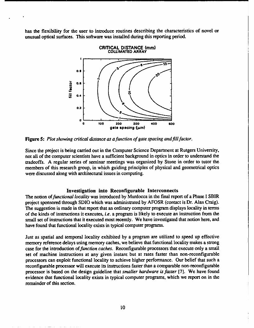
Critical Distance for Collimated ArrayAn example of the diffraction-based trade-offs in device spacing and propagation distanceis given for the case involving a collimated array of beams. The critical distance is afunction of the microlens diameter. For example, consider an array with a device spacingA = 200g•m and light of wavelength 0.85gm. If the lens is only 10pom in diameter (D/A =0.05), there will be a buffer zone of width B = 95pgm on each side of the microlens overwhich the light may spread before crossing into the neighboring channel. The diffractionspread angle of the beam from such a small lens, however, is large (4.9"), and after only Lc= 1.1rmm the beam begins to spread beyond the 95gm buffer and mix with the neighboringsignal. Similarly, as the microlens diameter approaches the gate spacing, the criticaldistance L, is also very small. Near this other extreme, if D/A = 0.95 (D=190gm) thediffraction angle is a much smaller .26, but the buffer zone width is now reduced toB=5gm, and Lc is again only 1.1 mm. However, for less extreme values of D/A (e.g.,near 0.5), Lc is much larger (nearly 6mm). Figure 5 shows a plot of L, (given inmillimeters) as a function of varied fill factor D/A and gate spacing A. Since the diffractionangle decreases with increasing lens diameter, one might suspect that low crosstalk couldbe maintained over longer distances if the full width A could be utilized for the microlensapertures. Effective use of these larger apertures can be accomplished by slightly focusingthe beam emerging from the microlens, thus avoiding the condition in which any spreadingof the collimated beam from a lens with D = A results in crosstalk.
This focused array configuration is discussed in the book chapter, as well as several other resultsof Stone's study.
The micro/macro-optics study has been useful in identifying applications that are best served withconventional optics, and those where diffractive optics are more reasonable to apply. This aspectof Stone's work influences the design of digital circuits, and we are now using the XOPID tool toinvestigate the architectural implications of using various combinations of micro and macro-optics.
The perspective of classic lens design is an important approach to studying both conventional anddiffractive optics, and to that end, the OSLO Series 2 lens design program was purchased usingcost-sharing funds which were provided by Rutgers for this grant. The software is important as aresearch tool for studying the properties of new elements and new configurations. For example, it
9
has the flexibility for the user to introduce routines describing the characteristics of novel orunusual optical surfaces. This software was installed during this reporting period.
CRITICAL DISTANCE (mm)COLLIMATED ARRAY
* 1
0.2
0
00 100 200 300 400 500
gate spacing (jro)
Figure 5: Plot showing critical distance as a function of gate spacing and fillfactor.
Since the project is being carried out in the Computer Science Department at Rutgers University,not all of the computer scientists have a sufficient background in optics in order to understand thetradeoffs. A regular series of seminar meetings was organized by Stone in order to tutor themembers of this research group, in which guiding principles of physical and geometrical opticswere discussed along with architectural issues in computing.
Investigation into Reconfigurable InterconnectsThe notion of functional locality was introduced by Murdocca in the final report of a Phase I SBIRproject sponsored through SDIO which was administrated by AFOSR (contact is Dr. Alan Craig).The suggestion is made in that report that an ordinary computer program displays locality in termsof the kinds of instructions it executes, i.e. a program is likely to execute an instruction from thesmall set of instructions that it executed most recently. We have investigated that notion here, andhave found that functional locality exists in typical computer programs.
Just as spatial and temporal locality exhibited by a program are utilized to speed up effectivememory reference delays using memory caches, we believe that functional locality makes a strongcase for the introduction of function caches. Reconfigurable processors that execute only a smallset of machine instructions at any given instant but at rates faster than non-reconfigurableprocessors can exploit functional locality to achieve higher performance. Our belief that such areconfigurable processor will execute its instructions faster than a comparable non-reconfigurableprocessor is based on the design guideline that smaller hardware is faster [7]. We have foundevidence that functional locality exists in typical computer programs, which we report on in theremainder of this section.
10

Measurements of instruction set usageHennessy and Patterson [7] report on the instruction set usage for a number of applicationprograms running on different architectures, and one of their conclusions is that programs use onlya small part of the total instruction set provided by the architecture, and that an even smaller set ofinstructions (about twelve or so) account for as much as 80% of the total number of instructionsexecuted. This observation motivated us to look for functional locality in programs. Our study iscarried out in two parts. We look first at the extent of functional locality that arises solely from thefact that some instructions are executed more often than others. In this part of the study, using therun-time frequency count information collected in the instruction usage study reported in Ref. [71,we synthesized random runs with uniform frequency distributions of machine instructionsmatching those reported, and studied the hit-ratio that a reconfigurable processor would achieve fordifferent sizes of the function cache using a first-in-first-out (FIFO) instruction replacementstrategy. It should be emphasized here that it is the actual hardware that is being replaced, and notsimply the codewords that represent instructions. This part of the study uses two architectures -the DEC VAX, and the DLX, which is a generic Load/Store architecture described in Ref. [7].Three different programs are used on each machine: gcc (a C compiler), spice (a circuitsimulator), and tex (a text formatter).
Figure 6 shows a plot of hit-ratio against code size for the DLX running gcc for different functioncache sizes. Plots for spice and tex for the DLX, and also for these three programs on the VAXare nearly identical in form to Figure 6. For our purposes, the hit-ratio is the percentage of the totalinstructions executed for which reconfiguration is required assuming that at any given instant, theprocessor implements only as many instructions as the size of the function cache allows andreconfigures itself to implement an instruction that is not in the function cache. In each case the hit-ratio increases as the function cache size increases but is almost completely insensitive to code size.For this reason, we use a code size of no more than 1,000,000 machine instructions for themeasurements that follow.
Figure 7 shows plots of hit ratios as functions of cache sizes for the DLX and the VAX,respectively, for synthesized runs based on the instruction mixes found in gcc, spice, and tex.As shown in the plots, high hit ratios are obtained for small cache sizes. Motivated by theseresults, we developed software tools for the second part of the study, which allowed us to gatherentire runs of some sample programs. The architecture used for this part of the study is theSPARC based Sun-4 and the programs studied are latex and the gcc components: gcc-cpp,gcc-ccl, as and Id. Collecting a program trace in this fashion slows down the program beingtraced by a large factor. For example, one trace of seven million instructions required nine hoursof actual time. For this reason, the programs were executed using small sample files. Figure 8shows the effect of changing the size of the function cache on the hit-ratio for different programs.For the programs shown in Figure 8, we also gathered data on the run-time frequency distribution,generated runs with matching frequency distributions and studied the effect of function cache sizeon hit-ratio. Our observations are shown in Figure 9. Note that the hit-ratio values we see inFigure 8 are higher than corresponding values seen in Figure 9 for the same function cache size.This indicates that the programs in our study exhibit functional locality to a higher degree thanwould be exhibited simply because programs execute some instructions more often than others.
11

'"I I I I T
-- - -noI - --
Itam
aUSmSm4m-
""m
-11 1 I--L -
i i i i IIMEN"
Figure 6: Hit ratio versus code sizefor different sizes of the function cache for synthesized runsof gcc on the DLX.
9112
NA - Um
7WA
MA -
xm
4m - A
Ism - aM
IOI -I II
Figure 7: Hit ratio as a function of the size of the function cache for synthesized runs on the DLX(left), and the VAX (right).
12

go-
.... ... .... ..
40 Id
30
FUaNWRcuam sin a~ (is isaumcdM~)
Figure 8: Hit ratio as afunction of the size of the function cache for actual runs on the SPARC.
ISO
! I
Pumioc cus us (sabuuum)
Figure 9: Hit ratio as a function of the size of the function cache for synthesized runs on theSPARC.
DiscussionThe data we have collected provides evidence for the existence of functional locality in ordinaryprograms. Based on the evidence, we claim that a reconfigurable processor that modifies itshardware to execute a slowly changing set of machine instructions can exploit functional locality toachieve higher performance than a non-reconfigurable processor. In order to quantify the
13

performance gain, we define P (> 1) as the ratio by which the execution of an instruction which isnot in the function cache is slowed down compared to the execution of an instruction in the cache.The factor by which a reconfiguring multiprocessor is slowed down because of misses is thengiven by slowdown = h + P x (I - h) where h is the hit-ratio. If a (< 1) is the ratio of the speedwith which the reconfigurable processor executes an instruction that it finds in its cache to thespeed at which a non-reconfigurable processor executes an instruction, then in order for thereconfigurable processor to be faster than the non-reconfigurable processor, a should be less than
I . From Figure 10, it is clear that the higher the hit-ratio, the lesser the sensitivity of theslowdownslowdown factor to the cost of reconfiguration. We choose a sample point 13 = 5, based on theexpected reconfiguration time as compared to the bit rate of matrix addressable devices which arebeing developed at PRI under NASA support. We choose h near 0.8 which is typical forexecution runs we have observed. This sample point gives us a slowdown of 2, which means thatthe processor runs twice as slow as a result of misses than it would run if there were no misses atall. A reconfigurable processor is assumed to be faster than a non-reconfigurable processor as aresult of its reduced size, however, and so the speedup must compensate for the slowdown. Theoperating region in which a reconfigurable approach breaks even is shown for this sample point inFigure 11. In order for the reconfigurable processor to break even, it must execute instructions attwice the rate of a non-reconfigurable processor.
9
8 Hit ratio (h)= 0.20
7Sample point: 0 S 0.30 6 Slowdown ..2_ - h 0.180.•
0593
1
0 1 2 3 4 5 6 7 8 910Reconfiguration time ( P)
Figure 10: Slowdown factor as a function of the reconfiguration cost and hit-ratio.
A potentially significant application of these results is for the DOC II optical processor underdevelopment at OptiComp. The DOC II processor is being developed for a SPARC-likeinstruction set, but only a subset of the instruction set can be implemented at any one time. Thestudy reported here can be used both to determine how to organize the cache (the DOC IIinstruction mask) and to characterize the effectiveness of the strategy.
14

4
3 Break-even (saRi fast
. 2
~~~. 2........**.
1 2 3 4Speedup
Figure 11: Break-even operating region in which the slowdown that resulzs from cache misses iscompensated by the speedup due to the smaller size of the processor.
Collaboration with NECDuring the past year, we have created a formal collaboration with NEC Research Institute inPrinceton. Dr. Eugen Schenfeld at NEC has made arrangements to support Ph.D. student VipulGupta for 50% of his time, starting in July 1992. A collaboration has already been underway forseveral weeks, primarily between Gupta and Schenfeld, in the area of reconfigurable opticalinterconnects.
Gupta is investigating a model that consists of a two level, crossbar based interconnectionnetwork. This network consists of a large number of small (8x8 or 16x16) fast electronic crossbarswitches at Level 1 which are connected by a very large but slow switching optical crossbar atLevel 2. Processing elements connect directly to the fast switches in Level 1 and communicationbetween processing elements attached to distinct Level 1 switches goes first through a fast switchat Level 1, then a slow switching optical network at Level 2, and then finally another fast switch atLevel 1.
Multiprocessors connected in a large variety of classical topologies like trees, rings, hypercubesand meshes can be partitioned into a large number of small clusters in such a fashion that assigningeach cluster to a Level 1 switch would result in a network configuration at Level 2 that does notneed to be switched very often. This lets the interconnection network combine the fast switchingspeed of the smaller electronic switches with the high connectivity and bandwidth of a large opticalnetwork.
The main problem for this method is to partition a graph representing the communication structureof multiprocessors into clusters exhibiting the property mentioned above. A clustering algorithmbased on probabilistic hill-climbing ha3 been designed and implemented. Preliminary results oncommunication graphs of up to 500 nodes arranged in 2-D meshes, binary trees, ternary trees, andhypercubes are encouraging. The Level 2 switch is considered to be optical, because of the large
15

bandwidth requirement, and because switching only needs to be handled infrequently with respectto the bit rate. Gupta is continuing his investigation in this area.
References[1] M. J. Murdocca, A. Huang, J. Jahns, and N. Streibl, "Optical Design of Programmable LogicArrays," Applied Optics, 27, pp. 1651-1660, (May 1, 1988).
[2] V. Gupta, "XOPID: An Interactive Design Tool for Digital Optical Circuits," (1992).
[31 See for example: J. L. Jewell, S. L. McCall, Y. H. Lee, A. Scherer, A. C. Gossard, and J.H. English, "Optical Computing and Related Microoptic Devices," Appl. Opt., 29, pp. 5050-5052(1990).
[4] K. Shiraishi, T. Sato, and S. Kawakami, "Experimental Verification of a Form-BirefringentPolarization Splitter," Appl. Phys. Lett., 58, pp. 211-212, (1991).
[5] A. W. Lohmann and S. 0. Sinzinger, "Spatial Noise Reduction in Array Illuminators," OSAOptical Computing Technical Digest Series, 6, pp. 38-40, (1991), (Digest from Topical Meetingon Optical Computing, March 4-6, Salt Lake City, Utah, 1991).
[6] D. Smith, M. Murdocca, and T. Stone, "Parallel Optical Interconnections," book chapter inOptical Computing Hardware, vol. 2, edited by S. Lee and J. Jahns, Academic Press, (1992), toappear.
[7] J. L. Hennessy and D. A. Patterson, Computer Architecture: A Quantitative Approach, MorganKaufmann Publishers, (1990).
PersonnelThe AFOSR/ONR contribution amounts to 200K for this reporting period, which is in addition to29K in cost-sharing from Rutgers University and several months of support for Murdocca. Thelabor breakdown for the year is summarized below. The notation X/Y represents X months workcontributed to the project with Y months charged to the AFOSR/ONR grant. When the monthscontributed exceed the months charged, the difference is contributed by Rutgers University. CS isan abbreviation for Computer Science and EE is an abbreviation for Electrical Engineering.
Person Time Title Background ContributionMiles Murdocca 6/0 Asst. Prof. CS/EE Project organization,
digital circuit design.
Thomas Stone 9/9 Res. Asst. Prof. Optical Science Diffractive optics studies.
Vipul Gupta 12112 Ph.D. student CS/EE Collision detection,circuit layout, functionallocality.
16

Masoud Majidi 12/12 Ph.D. student CS Algorithms forimplementing multiplefunctions, permutations.
Publications and PresentationsThe following publications and presentations were made during the past year. The AFOSR andONR sponsoring agencies are acknowledged in each publication. Some of the publications nameProf. Apostolos Gerasoulis and Ph.D. student Tao Yang as authors. Although these people arenot directly supported by the AFOSR/ONR grant, Rutgers University has made 97K in cost-sharing available to us in support of this grant, and we have used some of the cost-sharingresources to support their conference expenses since their work in parallel compiling supports ourinvestigation into reconfigurable optical interconnects. Prof. Donald Smith, who appears as a co-author in the first publication, developed a method of avoiding defects in optical logic arrays whichwas described in the previous annual report. His support for that year was provided by RutgersUniversity, which is in addition to the 97K in cost-sharing.
PublicationsD. Smith, M. Murdocca, and T. Stone, "Parallel Optical Interconnections," book chapter in OpticalComputing Hardware, vol. 2, edited by S. Lee and J. Jahns, Academic Press, (1992, to appear).
M. Murdocca and V. Gupta, "Architectural Implications of Reconfigurable Optical Interconnects,"submitted to: Journal of Parallel and Distributed Computing.
M. Murdocca and A. Sharma, "An application of optically reconfigurable interconnects to thedataflow parallel computing paradigm," SPIE Proceedings of OE/Aerospace, Advances in OpticalInformation Processing V, (Apr. 1992).
M. Murdocca "Architectural implications of optical computing," Proceedings of the 12th GIITGConference on Architecture of Computing Systems, Kiel, Germany, (Mar. 1992).
M. Murdocca and S. Levy, "Design of a Gaussian Elimination Architecture for the DOC IIProcessor," 1991 OE-Lase Symposium, (Jul. 1991).
T. Yang and A. Gerasoulis, "PYRROS: Static Task Scheduling and Code Generation for MessagePassing Multiprocessors," ACM International Conference on Supercomputing, (July 1992, toappear).
A. Gerasoulis and T. Yang, "On the Granularity and Clustering of Directed Acyclic Task Graphs,"Submitted to: IEEE Transactions on Parallel and Distributed Systems.
A. Gerasoulis and T. Yang, "Automatic Program Scheduling for Distributed Memory ScalableArchitectures," Submitted to: CONPAR92/VAPPV Conference, (Sep. 1992).
17

A. Gerasoulis and T. Yang, "Scheduling Program Task Graphs on MIMD Architectures," toappear as a book chapter in Algorithm Derivation and Program Transformation, edited by R.Paige, J. Reif, and R. Wachter, Kluwer, (1992).
PresentationsT. Stone (presenter) and J. Battiato, "Spot-Array Generation and Optical Interconnection UsingBirefringent Crystals," Opt. Soc. Am. Annual Meeting, San Jose, California, (Nov. 3-8, 1991).
T. Stone, "Quadratic Optical Pulse Compressor," Opt. Soc. Am. Annual Meeting, San Jose,California, (Nov. 3-8, 1991).
M. Murdocca (presenter) and A. Sharma, "An application of optically reconfigurable interconnectsto the dataflow parallel computing paradigm," SPIE OE/Aerospace, Orlando, (Apr. 1992).
M. Murdocca, "Architectural implications of optical computing," The 12th GI/ITG Conference onArchitecture of Computing Systems, Kiel, Germany, (Mar. 1992).
M. Murdocca (presenter) and S. Levy, "Design of a Gaussian Elimination Architecture for theDOC II Processor," 1991 OE-Lase Symposium, San Diego, (Jul. 1991).
M. Murdocca, "Architectural Implications of Reconfigurable Optical Interconnects," presented atthe Boulder Workshop on Optical Interconnects, (Feb. 1992).
A. Gerasoulis, 10th Parallel Circus, Oak Ridge National Lab, (Oct. 1991).
A. Gerasoulis, ACM/IEEE Supercomputing '91, Albuquerque, New Mexico, (Nov. 1991).
A. Gerasoulis, IEEE Scalable High Performance Computing Conference SHPCC-92,Williamsburg, (Apr. 1992).
A. Gerasoulis, ACM International Conference on Supercomputing (ICS92), Washington, (Jul.1992).
Patent Disclosures
The following patent disclosures were made during the past year:
T. Stone, "Birefringent Array Generator and Birefringent Optical Interconnector."
T. Stone, "Achromatic and Dispersive Retarders and Compensators."
Plans for Future WorkThe work planned for the final year on optical interconnects involves a continuation of the tradeoffinvestigation relating optical and architectural complexity, which will make use of the CAD tools.Emphasis will be on combined micro/macro approaches that retain dense element spacing whileminimizing crosstalk. Diffractive and refractive lens modeling will continue, and the OSLOsoftware is expected to be an important asset in this investigation. Birefringent interconnects,
18

although a comparatively simple concept, have distinct advantages including efficiency, scalability,and low dispersion. A publication on this approach will be submitted early in the final year, andwork will continue in studying the impact such interconnects can have in the optical/architecturaltradeoffs. The low dispersion nature of these interconnects may be very useful for interconnectingmicrolaser or other devices where wavelength variations can be an impediment to high dispersiondiffractive interconnects. In this context other achromatization techniques for interconnects willalso be studied, including hybrid diffractive/refractive elements and an evaluation of theapplicability of the achromatic retarder. The laboratory facility (built from matching funds fromthis contract) for studying interconnects and fabricating diffractive elements will be operable duringthe final year and will be used for feasibility experiments.
Gupta and Murdocca plan to continue their investigation into reconfigurable interconnects, and tocharacterize situations in which reconfiguration can be exploited in order to improve speed ordensity. Any algorthms or design techniques that result from this investigation will beincorporated into the CAD tools.
An extensive software task lies ahead in making the tools more user friendly, and in refining thetools to conform to practical considerations that arise in laboratory experiments. For example, thetools are being used in a Rome Laboratory sponsored SBIR effort for the design of an all-opticalGaussian elimination processor. Some of the practical problems that have been discovered that thetools do not address are:
1) The need for a simulator that supports functional modeling and debugging of logic circuits.
2) The need to XY-fold rectangular circuit designs (this is the shape that the CAD tools produce)onto square logic arrays.
3) The need to Z-fold OR-NOR circuit designs into the linear order supported by arrays (e.g. OR-OR-NOR-repeat may be all that is supported when OR-NOR-OR-NOR is needed). A related issueis the need to automate the mapping of associative logic (such as AND and OR) onto non-associative logic arrays (such as NOR).
4) An implementation of Smith's fault-avoidance algorithms which were discussed in the previousAnnual Report.
Although we would like to address these practical considerations at Rutgers, it poses aconsiderable time investment for the Ph.D. students, which will hinder their investigations inhigher payoff research such as reconfigurable interconnects and better layout strategies. As analternative, we took advantage of an opportunity that came about through the SBIR program. Thetools will be upgraded through the help of two programmers who are being funded through aPhase II SBIR effort at Rome Laboratory (Project Engineer is Robert Kaminski 315-330-4092).This effort will be supervised by Murdocca to ensure a smooth transition of the tools from Rutgersto Rome Laboratory.
19

ConclusionThe most significant accomplishments for the period include (1) the development of a CAD toolpackage for digital optical circuit design, (2) the development of function caching, which exploitsproperties of reconfigurable optical interconnects (3) an investigation into micro vs. macro opticaltradeoffs, and (4) increasing the number of functions that can be implemented on a PLA. Atransfer of technology took place to Rome Laboratory for Stone's work in birefringentinterconnects and spot-array generation, which resulted in one of two patent disclosures for theyear.
Miles Murdocca
20


![2017 Honda SUVs & Crossovers [Infographic] | MS Honda](https://img.pdfslide.us/doc/110x75/58f3684f1a28ab59438b4607/2017-honda-suvs-crossovers-infographic-ms-honda.jpg)