Embed Size (px)
Citation preview
9th Sept, 20091
VLSI Design & Test seminar series, Fall 2009, Auburn University, Auburn, AL
Low Power Implementation of ARM1176JZF-S
by
Manish Kulkarni
2 9th Sept, 2009
VLSI Design & Test seminar series, Fall 2009, Auburn University, Auburn, AL
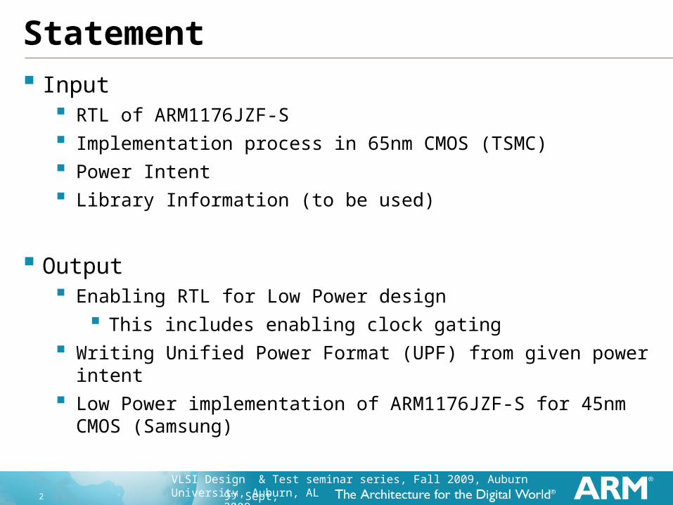
Statement Input
RTL of ARM1176JZF-S
Implementation process in 65nm CMOS (TSMC)
Power Intent
Library Information (to be used)
Output Enabling RTL for Low Power design
This includes enabling clock gating
Writing Unified Power Format (UPF) from given power intent
Low Power implementation of ARM1176JZF-S for 45nm CMOS (Samsung)
3 9th Sept, 2009
VLSI Design & Test seminar series, Fall 2009, Auburn University, Auburn, AL
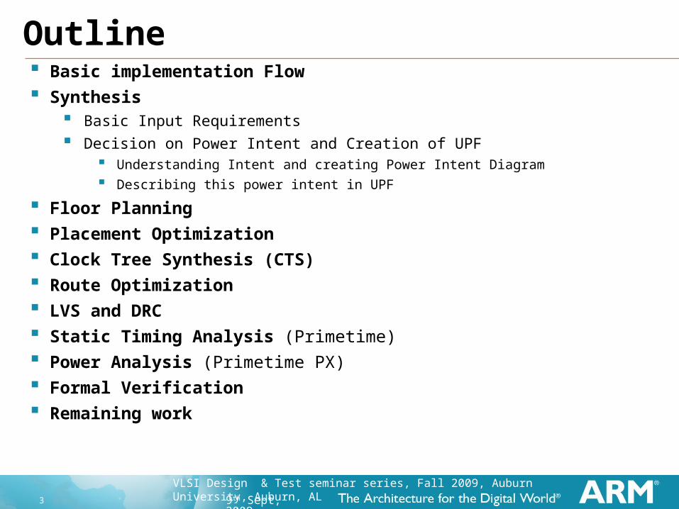
Outline Basic implementation Flow
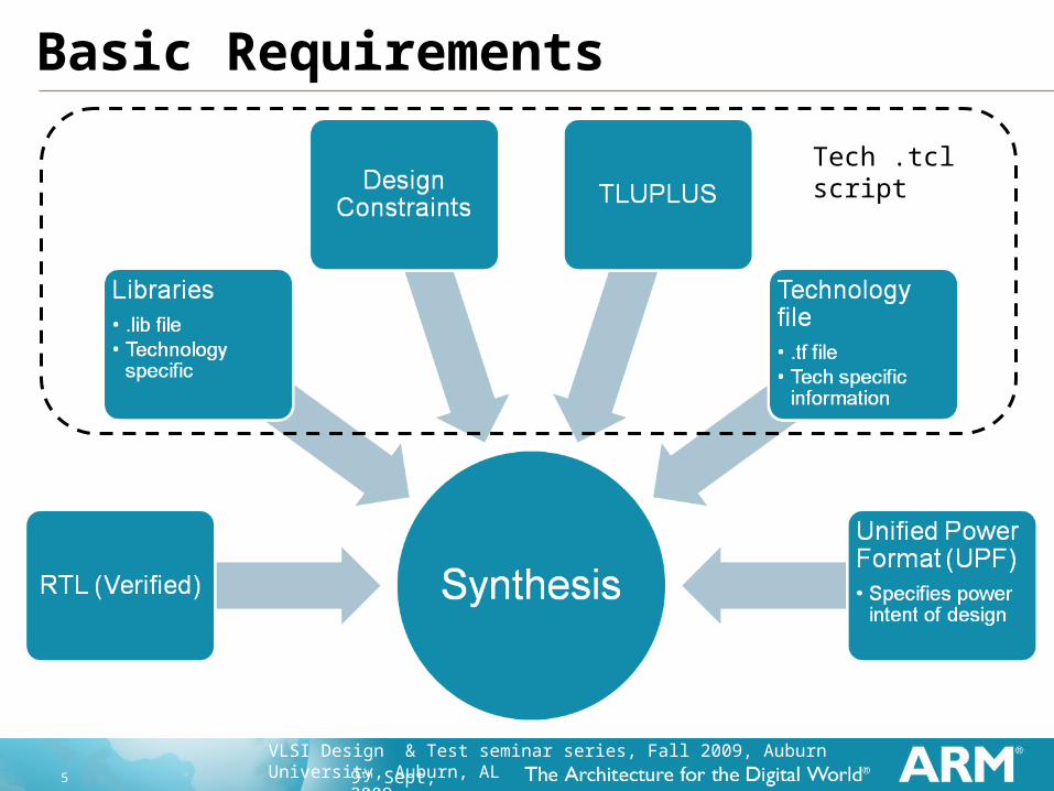
Synthesis Basic Input Requirements
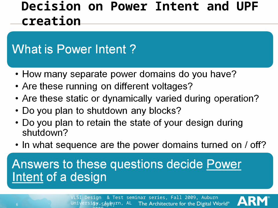
Decision on Power Intent and Creation of UPF Understanding Intent and creating Power Intent Diagram
Describing this power intent in UPF
Floor Planning
Placement Optimization
Clock Tree Synthesis (CTS)
Route Optimization
LVS and DRC
Static Timing Analysis (Primetime)
Power Analysis (Primetime PX)
Formal Verification
Remaining work
4 9th Sept, 2009
VLSI Design & Test seminar series, Fall 2009, Auburn University, Auburn, AL
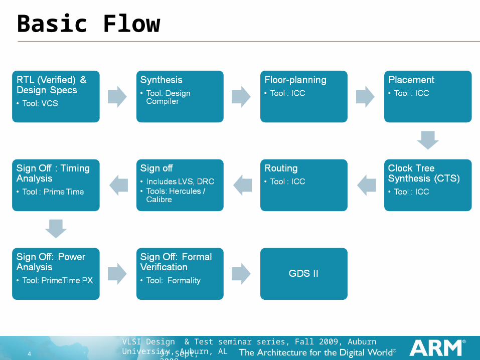
Basic Flow
5 9th Sept, 2009
VLSI Design & Test seminar series, Fall 2009, Auburn University, Auburn, AL
Basic Requirements
Tech .tcl script
6 9th Sept, 2009
VLSI Design & Test seminar series, Fall 2009, Auburn University, Auburn, AL
Decision on Power Intent and UPF creation
7 9th Sept, 2009
VLSI Design & Test seminar series, Fall 2009, Auburn University, Auburn, AL
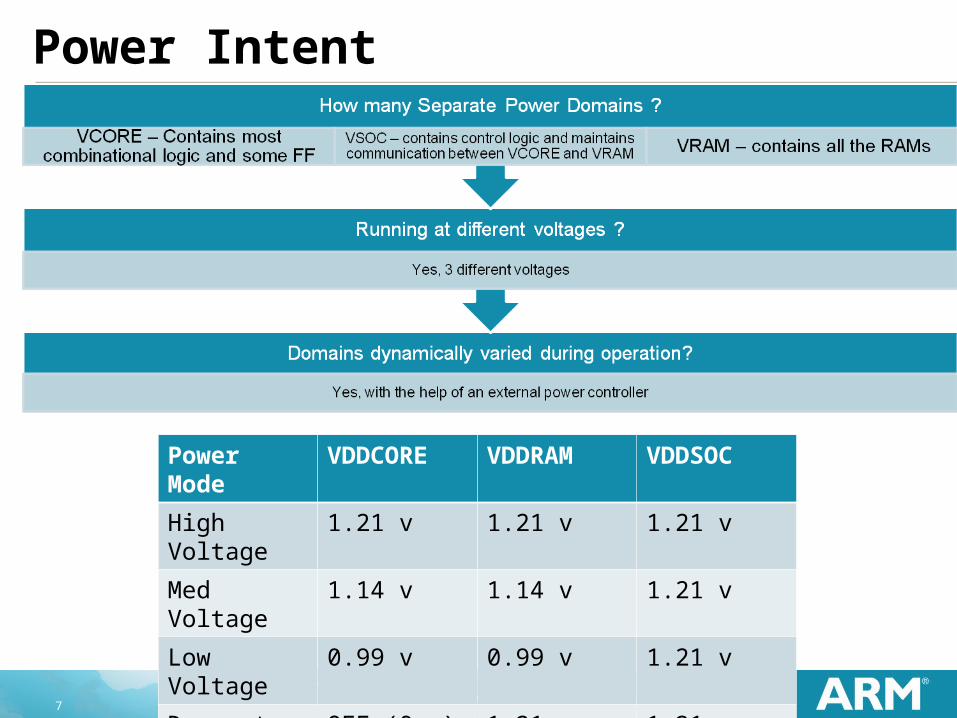
Power Intent
Power Mode
VDDCORE VDDRAM VDDSOC
High Voltage 1.21 v 1.21 v 1.21 v
Med Voltage 1.14 v 1.14 v 1.21 v
Low Voltage 0.99 v 0.99 v 1.21 v
Dormant OFF (0 v) 1.21 v 1.21 v

8 9th Sept, 2009
VLSI Design & Test seminar series, Fall 2009, Auburn University, Auburn, AL

9 9th Sept, 2009
VLSI Design & Test seminar series, Fall 2009, Auburn University, Auburn, AL
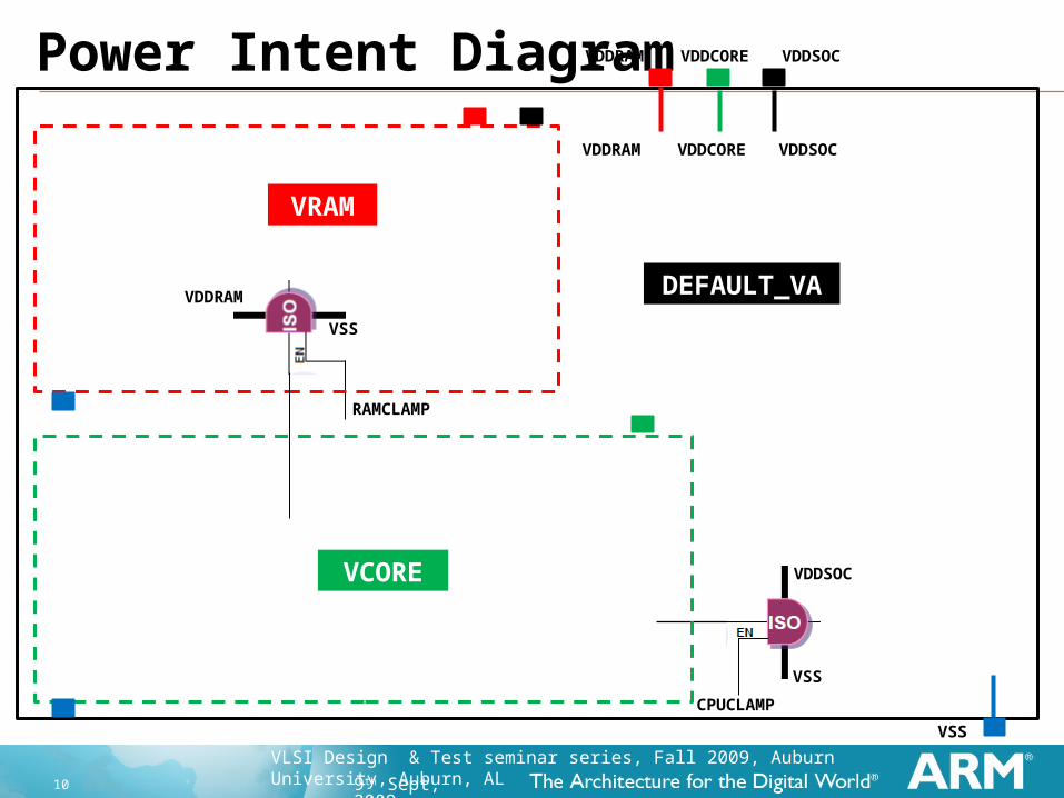
Power Intent Diagram
VCORE
VRAM
DEFAULT_VA
VDDCORE VDDSOCVDDRAM
VDDCORE VDDSOCVDDRAM
VSS
10 9th Sept, 2009
VLSI Design & Test seminar series, Fall 2009, Auburn University, Auburn, AL
Power Intent Diagram
VSS
VDDSOC
CPUCLAMP
VSS
VDDRAM
RAMCLAMP
VCORE
VRAM
DEFAULT_VA
VDDCORE VDDSOCVDDRAM
VDDCORE VDDSOCVDDRAM
VSS

11 9th Sept, 2009
VLSI Design & Test seminar series, Fall 2009, Auburn University, Auburn, AL
Power Intent Diagram
VSS
VSS
VDDSOC
VDDRAM
VSS
VDDSOC
VDDCORE
VDDSOC
CPUCLAMP
VSS
VDDRAM
RAMCLAMP
VCORE
VRAM
DEFAULT_VA
VDDCORE VDDSOCVDDRAM
VDDCORE
VDDSOCVDDRAM
VSS
LS
LS
VDDRAM
VSS
VSS
VDDCORE
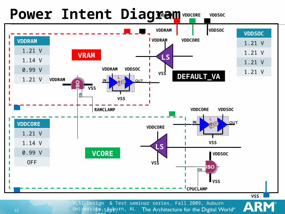
12 9th Sept, 2009
VLSI Design & Test seminar series, Fall 2009, Auburn University, Auburn, AL
Power Intent Diagram
VDDCORE
1.21 V
1.14 V
0.99 V
OFF
VDDRAM
1.21 V
1.14 V
0.99 V
1.21 V
VDDSOC
1.21 V
1.21 V
1.21 V
1.21 V
VSS
VSS
VDDSOC
VDDRAM
VSS
VDDSOC
VDDCORE
VDDSOC
CPUCLAMP
VSS
VDDRAM
RAMCLAMP
VCORE
VRAM
DEFAULT_VA
VDDCORE VDDSOCVDDRAM
VDDCORE
VDDSOCVDDRAM
VSS
VDDRAM
VSS
VSS
VDDCORE
LS
LS

13 9th Sept, 2009
VLSI Design & Test seminar series, Fall 2009, Auburn University, Auburn, AL
UPFPower Intent
Diagram
Writing UPF from Power Intent Diagram
14 9th Sept, 2009
VLSI Design & Test seminar series, Fall 2009, Auburn University, Auburn, AL
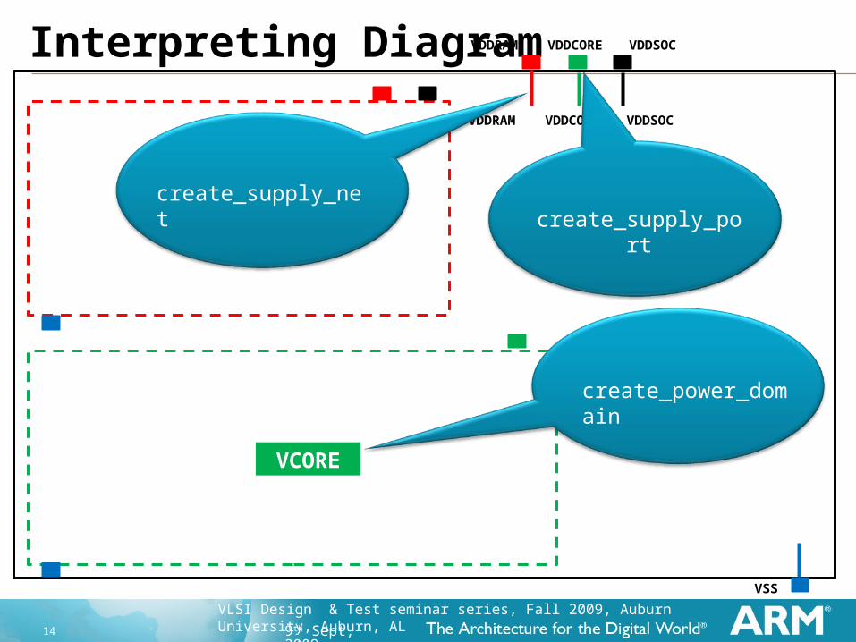
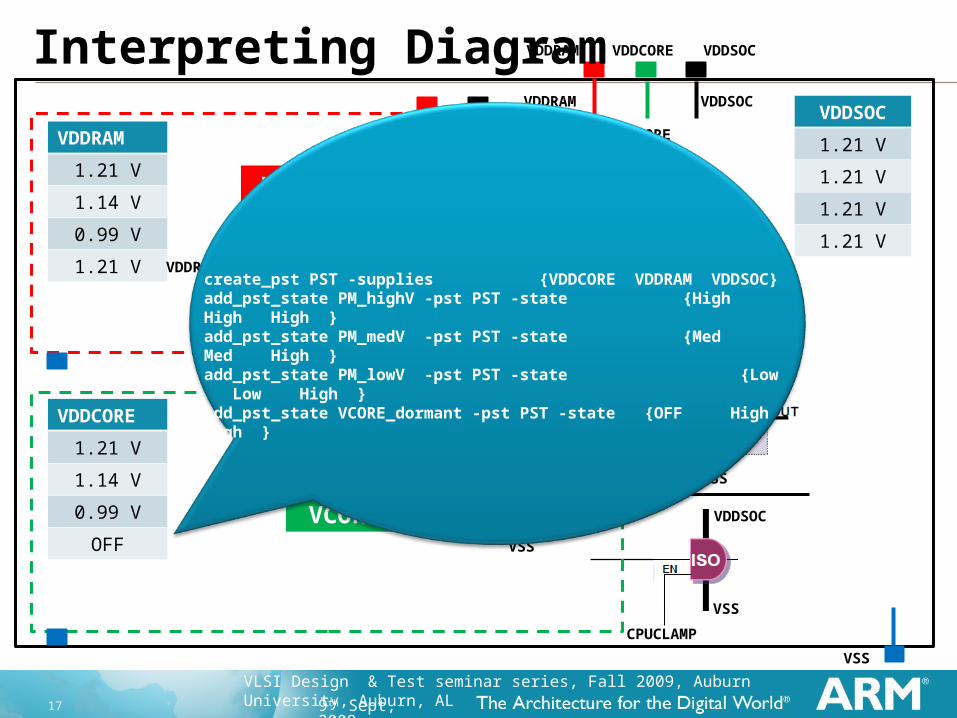
Interpreting Diagram
VCORE
VRAM
DEFAULT_VA
VDDCORE VDDSOCVDDRAM
VDDCORE VDDSOCVDDRAM
VSS
create_supply_net
create_power_domain
create_supply_port
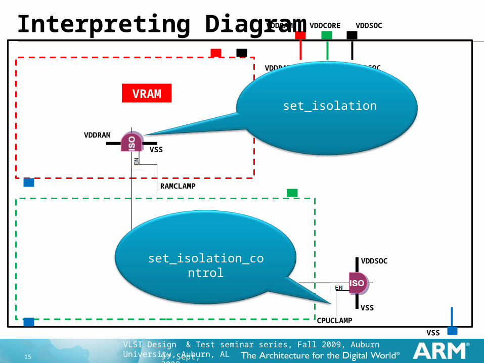
15 9th Sept, 2009
VLSI Design & Test seminar series, Fall 2009, Auburn University, Auburn, AL
VSS
VDDSOC
CPUCLAMP
VSS
VDDRAM
RAMCLAMP
VCORE
VRAM
DEFAULT_VA
VDDCORE VDDSOCVDDRAM
VDDCORE VDDSOCVDDRAM
VSS
set_isolation
set_isolation_control
Interpreting Diagram
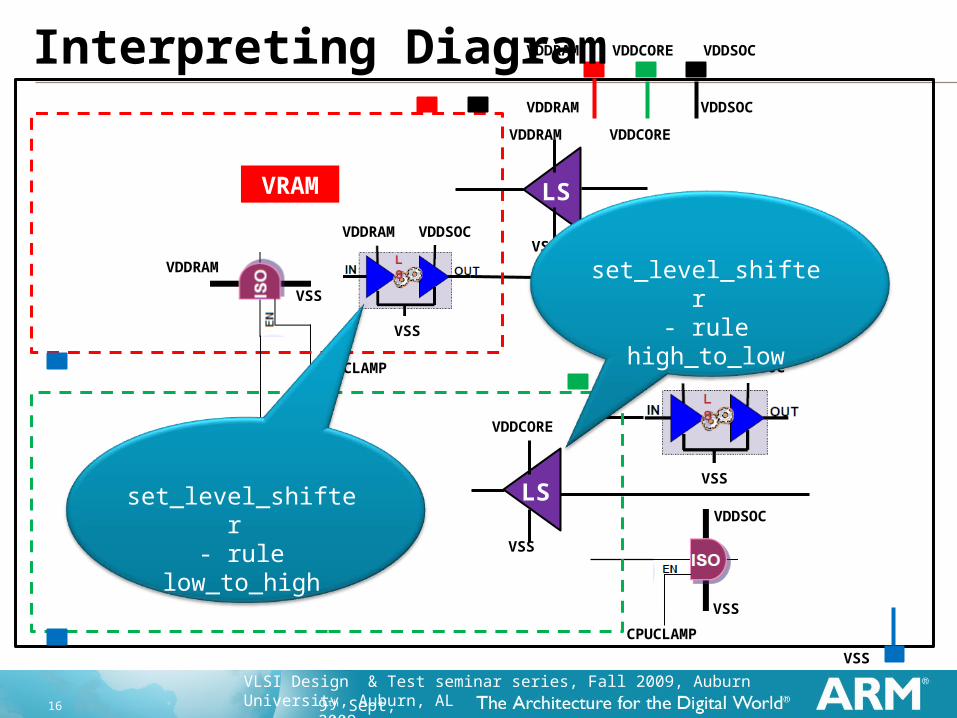
16 9th Sept, 2009
VLSI Design & Test seminar series, Fall 2009, Auburn University, Auburn, AL
VSS
VSS
VDDSOC
VDDRAM
VSS
VDDSOC
VDDCORE
VDDSOC
CPUCLAMP
VSS
VDDRAM
RAMCLAMP
VCORE
VRAM
DEFAULT_VA
VDDCORE VDDSOCVDDRAM
VDDCORE
VDDSOCVDDRAM
VSS
LS
LS
VDDRAM
VSS
VSS
VDDCORE
set_level_shifter - rule low_to_high
set_level_shifter - rule high_to_low
Interpreting Diagram
17 9th Sept, 2009
VLSI Design & Test seminar series, Fall 2009, Auburn University, Auburn, AL
VDDCORE
1.21 V
1.14 V
0.99 V
OFF
VDDRAM
1.21 V
1.14 V
0.99 V
1.21 V
VDDSOC
1.21 V
1.21 V
1.21 V
1.21 V
VSS
VSS
VDDSOC
VDDRAM
VSS
VDDSOC
VDDCORE
VDDSOC
CPUCLAMP
VSS
VDDRAM
RAMCLAMP
VCORE
VRAM
DEFAULT_VA
VDDCORE VDDSOCVDDRAM
VDDCORE
VDDSOCVDDRAM
VSS
VDDRAM
VSS
VSS
VDDCORE
LS
LS
create_pst PST -supplies {VDDCORE VDDRAM VDDSOC}add_pst_state PM_highV -pst PST -state {High High High }add_pst_state PM_medV -pst PST -state {Med Med High }add_pst_state PM_lowV -pst PST -state {Low Low High }add_pst_state VCORE_dormant -pst PST -state {OFF High High }`
Interpreting Diagram
18 9th Sept, 2009
VLSI Design & Test seminar series, Fall 2009, Auburn University, Auburn, AL
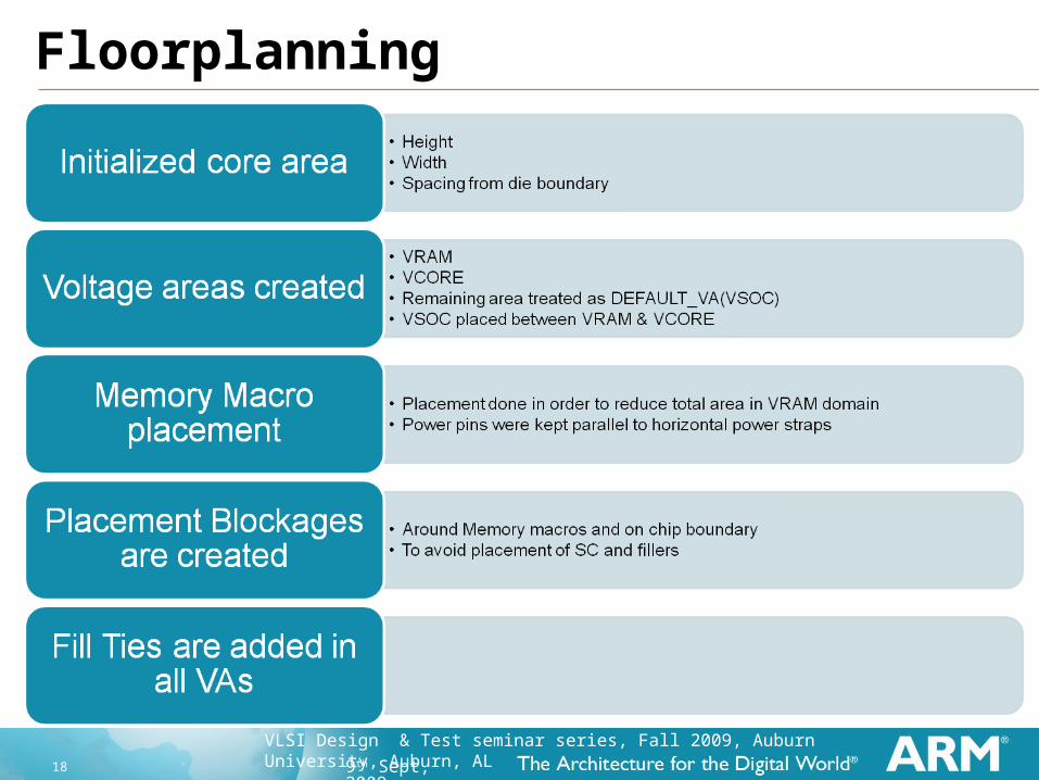
Floorplanning

19 9th Sept, 2009
VLSI Design & Test seminar series, Fall 2009, Auburn University, Auburn, AL
Floorplanning (Cont..)
20 9th Sept, 2009
VLSI Design & Test seminar series, Fall 2009, Auburn University, Auburn, AL
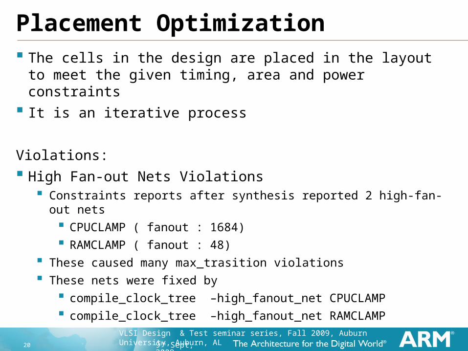
Placement Optimization The cells in the design are placed in the layout to meet the
given timing, area and power constraints
It is an iterative process
Violations:
High Fan-out Nets Violations Constraints reports after synthesis reported 2 high-fan-out nets
CPUCLAMP ( fanout : 1684)
RAMCLAMP ( fanout : 48)
These caused many max_trasition violations
These nets were fixed by
compile_clock_tree –high_fanout_net CPUCLAMP
compile_clock_tree –high_fanout_net RAMCLAMP
21 9th Sept, 2009
VLSI Design & Test seminar series, Fall 2009, Auburn University, Auburn, AL
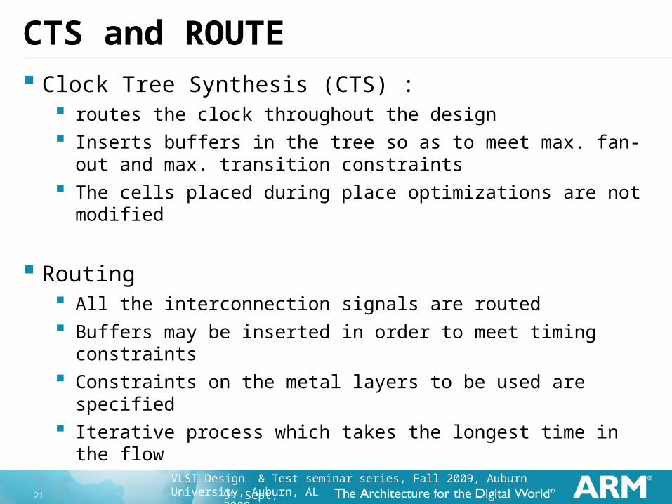
CTS and ROUTE Clock Tree Synthesis (CTS) :
routes the clock throughout the design
Inserts buffers in the tree so as to meet max. fan-out and max. transition constraints
The cells placed during place optimizations are not modified
Routing All the interconnection signals are routed
Buffers may be inserted in order to meet timing constraints
Constraints on the metal layers to be used are specified
Iterative process which takes the longest time in the flow
22 9th Sept, 2009
VLSI Design & Test seminar series, Fall 2009, Auburn University, Auburn, AL
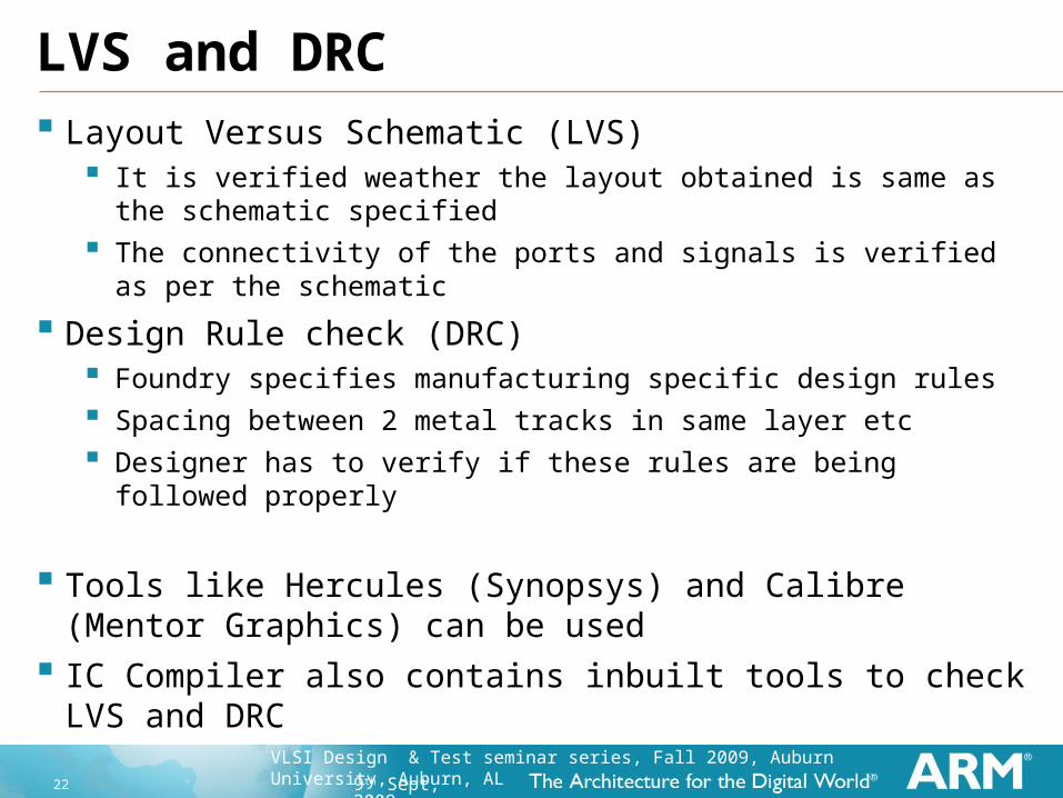
LVS and DRC Layout Versus Schematic (LVS)
It is verified weather the layout obtained is same as the schematic specified
The connectivity of the ports and signals is verified as per the schematic
Design Rule check (DRC) Foundry specifies manufacturing specific design rules
Spacing between 2 metal tracks in same layer etc
Designer has to verify if these rules are being followed properly
Tools like Hercules (Synopsys) and Calibre (Mentor Graphics) can be used
IC Compiler also contains inbuilt tools to check LVS and DRC

23 9th Sept, 2009
VLSI Design & Test seminar series, Fall 2009, Auburn University, Auburn, AL
Static Timing Analysis Analysis Performed using Primetime
Post Layout verilog netlist is loaded
Extracted Parasitic are loaded
Timing analysis is performed for only one power state (High voltage)
Violations:
Setup and Hold violations were found
Transition violations were found
These violations were fixed by adding buffers in high fan-out nets which are causing these violations
It can also be fixed by increasing the drive strength of cells

24 9th Sept, 2009
VLSI Design & Test seminar series, Fall 2009, Auburn University, Auburn, AL
Power Analysis Power Analysis is performed using Primetime PX
Probabilistic logic activity was used for power measurement and the probability was set to 0.25
Analysis was done only for first power state i.e. the high voltage mode
Power Group Internal(W)
Switching(W)
Leakage(W)
Total (Row)(W)
%
IO pad 0 0 0 0 0.00 %
memory 2.033e-03 5.632e-04 1.933e-04 2.789e-03 44.30%
clock_network 2.318e-04 1.105e-05 2.745e-04 5.174e-04 8.22%
register 6.903e-05 5.583e-06 3.601e-04 4.347e-04 6.90%
combinational 2.148e-04 1.777e-03 5.001e-04 2.492e-03 39.58%
sequential 4.312e-05 2.980e-06 1.690e-05 6.299e-05 1.00%
Total (Column) 2.591e-03 2.360e-03 1.345e-03 6.296e-03
41.16% 37.48% 21.36% 100.00%
25 9th Sept, 2009
VLSI Design & Test seminar series, Fall 2009, Auburn University, Auburn, AL
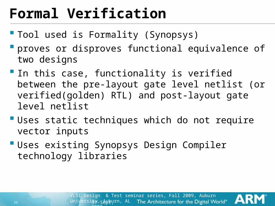
Formal Verification Tool used is Formality (Synopsys)
proves or disproves functional equivalence of two designs
In this case, functionality is verified between the pre-layout gate level netlist (or verified(golden) RTL) and post-layout gate level netlist
Uses static techniques which do not require vector inputs
Uses existing Synopsys Design Compiler technology libraries

26 9th Sept, 2009
VLSI Design & Test seminar series, Fall 2009, Auburn University, Auburn, AL
Remaining Work
Power State Voltages Power Frequency
VCORE VRAM VSOC
State_High 1.21 v 1.21 v 1.21 v 6.296 mW 250 MHz
State_Med 1.14 v 1.14 v 1.21 v ? ?
State_Low 0.99 v 0.99 v 1.21 v ? ?
Dormant 0 v 1.21 v 1.21 v ? ?
• The characterization was done for only High Power state • Similar characterization can be done for the other Power states

27 9th Sept, 2009
VLSI Design & Test seminar series, Fall 2009, Auburn University, Auburn, AL

28 9th Sept, 2009
VLSI Design & Test seminar series, Fall 2009, Auburn University, Auburn, AL