Embed Size (px)
Citation preview
1
8500 Service Manual
2-Feb-98
2
Specifications The Notebook Computer is a state-of-the-art, high performance, portable system. It offers a host of features specially designed to enhance performance and usability. : CPU
− Intel P54C/LM. − Intel P55C/LM with MMX technology.
: Memory − 3.3V power supply. − Supports Fast Page Mode/EDO/SDRAM. − 512KB secondary cache Pipeline Burst Synchronous RAM
(PBSRAM). − 8MB expandable up to 128MB. − 8/16/32/64MB 144-pin SODIMM RAM modules (option).
*(The x4 bit DRAM chips are not supported.)
: System BIOS − 256KB flash ROM. − PCI 2.1. − Plug and Play 1.0a.
: Display − 15.1” TFT XGA (1024x768 pixels) LCD panel available. − 13.8” DSTN XGA (1024x768 pixels) LCD panel available. − 4MB display memory (EDO). − Video Port Manager (VPM 1.10) for Zoomed Video (ZV) port. − Simultaneous display with an external monitor.
: Mass Storage − 3.5” floppy diskette drive (interchangeable). − 2.5” hard disk drive (12.7mm high or less). − 5.25” CD-ROM. − 2.5” (12.7mm high or less) or 3.0” (12.5mm high or less) secondary
hard disk drive (option). − 100MB Zip drive (15mm high) (option).
: Audio − Sound Blaster Pro compatible. − 3D stereo sound effects. − Stereo full duplex support. − 1MB ROM wavetable. − Built-in microphone. − Built-in speakers.

3
: PC Card Sockets − CardBus support. − ZV (Zoomed Video) port support. − Two Type II PC cards or one Type III PC card.
: Input/Output
− Built-in trackpad (PS/2). − Dual USB ports. − S-video jack for TV output. − 120-pin Expansion port. − RCA jack for video input. − External monitor (CRT) port. − Serial port. − Parallel port. − Dual PS/2 type ports. − Speaker-out jack. − Line-in jack. − Microphone-in jack.
: Infrared Wireless Communication − IrDA (HPSIR). − ASKIR. − Fast IR.
: Power Management − APM 1.2. − ACPI. − Global Standby. − Suspend and Resume.
: AC Power Supply
− AC input: 100~240VAC, 47~63Hz. − DC output: 20V. − Total output: 50W.
: Rechargeable Battery Pack − Li-ION battery available. − Battery low warning.
: Size & Weight − 357mm(w)x275mm(d)x50mm(h). − 4.5kg.
4
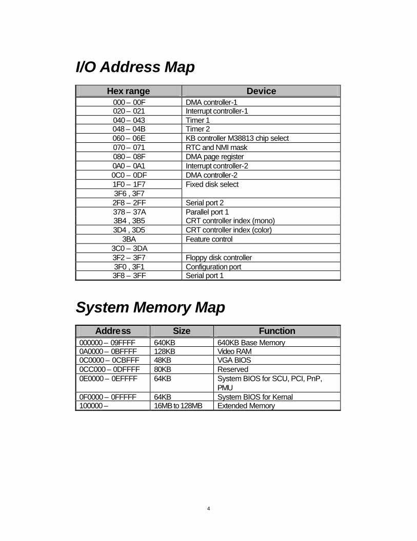
I/O Address Map
Hex range Device 000 – 00F DMA controller-1 020 – 021 Interrupt controller-1 040 – 043 Timer 1 048 – 04B Timer 2 060 – 06E KB controller M38813 chip select 070 – 071 RTC and NMI mask 080 – 08F DMA page register 0A0 – 0A1 Interrupt controller-2 0C0 – 0DF DMA controller-2 1F0 – 1F7 3F6 , 3F7
Fixed disk select
2F8 – 2FF Serial port 2 378 – 37A Parallel port 1 3B4 , 3B5 CRT controller index (mono) 3D4 , 3D5 CRT controller index (color)
3BA Feature control 3C0 – 3DA 3F2 – 3F7 Floppy disk controller 3F0 , 3F1 Configuration port 3F8 – 3FF Serial port 1
System Memory Map
Address Size Function 000000 – 09FFFF 640KB 640KB Base Memory 0A0000 – 0BFFFF 128KB Video RAM 0C0000 – 0CBFFF 48KB VGA BIOS 0CC000 – 0DFFFF 80KB Reserved 0E0000 – 0EFFFF 64KB System BIOS for SCU, PCI, PnP,
PMU 0F0000 – 0FFFFF 64KB System BIOS for Kernal 100000 – 16MB to 128MB Extended Memory
5
Motherboard The motherboard is designed mainly based on Pentium CPU and the Intel 430TX chipset; it includes the following features: ü 82439TX MTXC & 82371AB PIIX4 chipset solution from Intel. ü C&T 65555 Multimedia Flat Panel Controller. ü PCI Local Bus IDE interface. ü NS97338CR super I/O Controller. ü M38867 Keyboard Controller. ü Flash EPROM 256KB with SystemSoft system BIOS, VGA BIOS. ü DRAM Upgradable to 128MB. ü 7 DMA channels. ü 13 interrupt levels. ü Real Time clock / calendar, battery back up. ü Built-in 3D Stereo Audio subsystem. ü Built-in NTSC/PAL video-out S-jack. ü Built-in Video-in RCA-jack. ü IrDA infrared communication (Fast IR). ü Port connectors :
− 9 pin serial (COM1). − 25 pin parallel printer port (LPT1). − 15 pin external VGA port. − 6 pin external keyboard port. − 6 pin PS2 mouse. − 120 pin expansion port for Port Replicator. − 4 pin USB port x 2.

6
Microprocessor The Notebook Computer applied Intel Pentium SL-Enhanced or MMX (LM) microprocessor. P54C, P55C-133/150/166/200/233 (LM) Microprocessor The Intel Pentium Processor has an improved prefetch/BTB mechanism that is more accurate and aggressive than the P54C processor and the P55C CPU is built-in MMX (MultiMedia eXtension enable) Technology Architecture. Features included: ü Superscalar architecture. ü Separate code and data caches. ü Branch prediction. ü High performances floating point unit. ü Enhanced 64 bits data bus. ü Data integrity features. ü SL technology power management features. ü Multiprocessing support. ü Performance monitoring. ü Memory page size feature.
7
Chips Core Logic Chip – Intel 430TX 82439TX MTXC ü Support for Intel 586 CPU with bus speed up to 66MHz. ü Support for both symmetric and asymmetric type DRAM. ü High Performance Memory Controller. ü Enhanced hidden refresh. ü Support for Fast Page mode, EDO type, and Synchronous type DRAM. ü EDO RAM and SDRAM automatic detect mode. ü Support two bus mastering IDE channels. ü Serial IRQs supported. ü Synchronous SRAM Clock Control to reduce Power Consumption. ü Stop Grant, Stop Clock for 1X clock scaling. ü PCI local bus support. ü Flash EPROM support. ü Screen activity detect. ü Programmable suspend and resume. ü Automatic suspend timer. ü System activities and programmable clock speed control. ü Programmable system event. ü Programmable stop break event.
8
VGA Controller – Chips & Technology 65555 The C&T 65555 Multimedia Flat Panel Controller is a DRAM based, fully integrated LCD, CRT & TV 64 bits controller for PCI systems. It contains the following functions: ü Support displays with options for 2 and 4 MB. ü Support burst PCI and EDO/FPM memory. ü Support 16/24 bit color DSTNs up to 1024x768x16M color, and TFT
panels up to 1280x1024x64K color. ü Support non-interlaced 1600x1200x256, 1280x1024x64K, 1024x768x16M,
800x600x16M, and 640x480x16M color on CRT. ü Simultaneous display in 24 bit color on flat panel and CRT. ü Internal buffer provides flicker reduction. ü RGB signals driven from the C&T 65555 LUT/DAC can directly interface
with a standard off-the-shelf NTSC/PAL encoder. Composite synchronization signals support for standard home TV connection.
ü Graphic functions optimized by a 64 bit internal data bus and a four-color hardware cursor/pop-up icon operation up to 128x128x2 pixel image.
ü Provide flexible and extensive power management capabilities and support four states of VESA Display Power Management Signaling.
ü Video Modes supported.
9
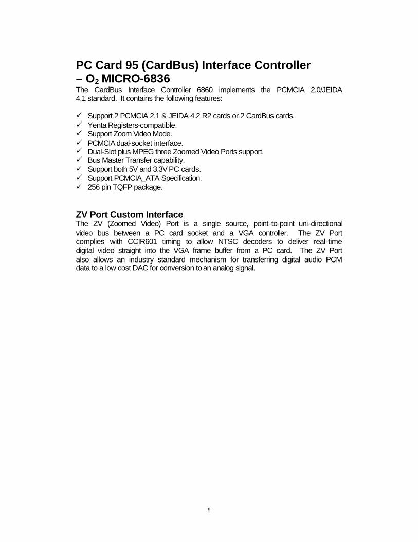
PC Card 95 (CardBus) Interface Controller – O2 MICRO-6836 The CardBus Interface Controller 6860 implements the PCMCIA 2.0/JEIDA 4.1 standard. It contains the following features: ü Support 2 PCMCIA 2.1 & JEIDA 4.2 R2 cards or 2 CardBus cards. ü Yenta Registers-compatible. ü Support Zoom Video Mode. ü PCMCIA dual-socket interface. ü Dual-Slot plus MPEG three Zoomed Video Ports support. ü Bus Master Transfer capability. ü Support both 5V and 3.3V PC cards. ü Support PCMCIA_ATA Specification. ü 256 pin TQFP package. ZV Port Custom Interface The ZV (Zoomed Video) Port is a single source, point-to-point uni-directional video bus between a PC card socket and a VGA controller. The ZV Port complies with CCIR601 timing to allow NTSC decoders to deliver real-time digital video straight into the VGA frame buffer from a PC card. The ZV Port also allows an industry standard mechanism for transferring digital audio PCM data to a low cost DAC for conversion to an analog signal.
10
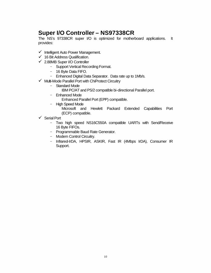
Super I/O Controller – NS97338CR The NS’s 97338CR super I/O is optimized for motherboard applications. It provides: ü Intelligent Auto Power Management. ü 16 Bit Address Qualification. ü 2.88MB Super I/O Controller
− Support Vertical Recording Format. − 16 Byte Data FIFO. − Enhanced Digital Data Separator. Data rate up to 1Mb/s.
ü Multi-Mode Parallel Port with ChiProtect Circuitry − Standard Mode
IBM PC/AT and PS/2 compatible bi-directional Parallel port. − Enhanced Mode
Enhanced Parallel Port (EPP) compatible. − High Speed Mode
Microsoft and Hewlett Packard Extended Capabilities Port (ECP) compatible.
ü Serial Port − Two high speed NS16C550A compatible UARTs with Send/Receive
16 Byte FIFOs. − Programmable Baud Rate Generator. − Modem Control Circuitry. − Infrared-IrDA, HPSIR, ASKIR, Fast IR (4Mbps IrDA), Consumer IR
Support.
11
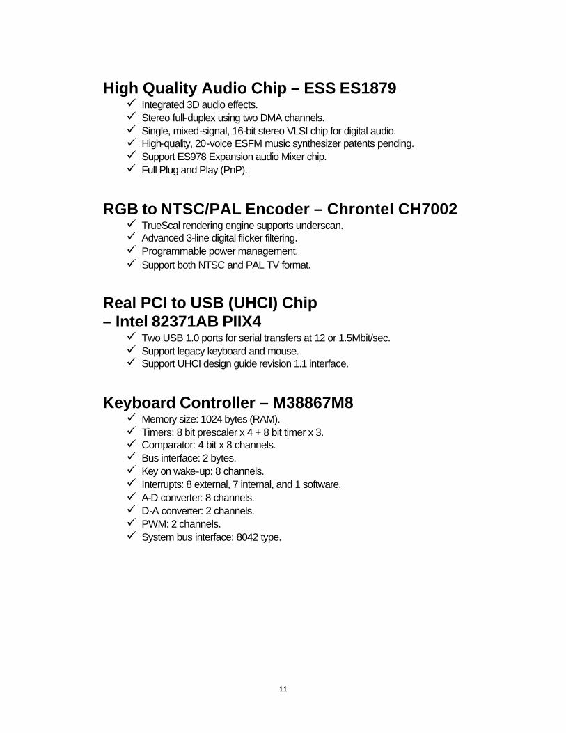
High Quality Audio Chip – ESS ES1879 ü Integrated 3D audio effects. ü Stereo full-duplex using two DMA channels. ü Single, mixed-signal, 16-bit stereo VLSI chip for digital audio. ü High-quality, 20-voice ESFM music synthesizer patents pending. ü Support ES978 Expansion audio Mixer chip. ü Full Plug and Play (PnP).
RGB to NTSC/PAL Encoder – Chrontel CH7002 ü TrueScal rendering engine supports underscan. ü Advanced 3-line digital flicker filtering. ü Programmable power management. ü Support both NTSC and PAL TV format.
Real PCI to USB (UHCI) Chip – Intel 82371AB PIIX4 ü Two USB 1.0 ports for serial transfers at 12 or 1.5Mbit/sec. ü Support legacy keyboard and mouse. ü Support UHCI design guide revision 1.1 interface.
Keyboard Controller – M38867M8 ü Memory size: 1024 bytes (RAM). ü Timers: 8 bit prescaler x 4 + 8 bit timer x 3. ü Comparator: 4 bit x 8 channels. ü Bus interface: 2 bytes. ü Key on wake-up: 8 channels. ü Interrupts: 8 external, 7 internal, and 1 software. ü A-D converter: 8 channels. ü D-A converter: 2 channels. ü PWM: 2 channels. ü System bus interface: 8042 type.
12
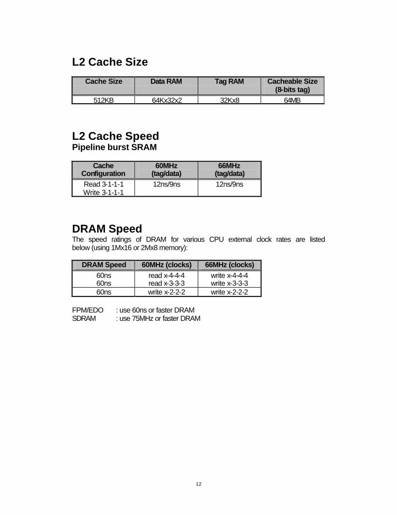
L2 Cache Size
Cache Size Data RAM Tag RAM Cacheable Size (8-bits tag)
512KB 64Kx32x2 32Kx8 64MB L2 Cache Speed Pipeline burst SRAM
Cache Configuration
60MHz (tag/data)
66MHz (tag/data)
Read 3-1-1-1 Write 3-1-1-1
12ns/9ns 12ns/9ns
DRAM Speed The speed ratings of DRAM for various CPU external clock rates are listed below (using 1Mx16 or 2Mx8 memory):
DRAM Speed 60MHz (clocks) 66MHz (clocks)
60ns read x-4-4-4 write x-4-4-4 60ns read x-3-3-3 write x-3-3-3 60ns write x-2-2-2 write x-2-2-2
FPM/EDO : use 60ns or faster DRAM SDRAM : use 75MHz or faster DRAM
13
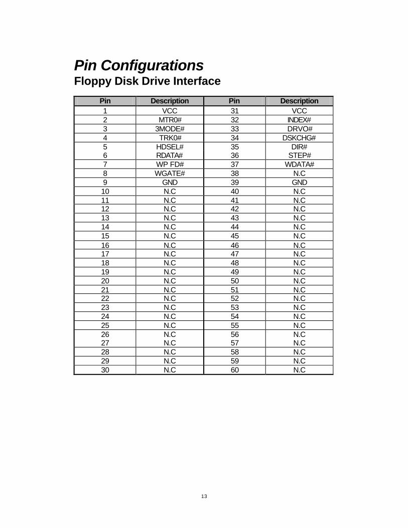
Pin Configurations Floppy Disk Drive Interface
Pin Description Pin Description 1 VCC 31 VCC 2 MTR0# 32 INDEX# 3 3MODE# 33 DRVO# 4 TRK0# 34 DSKCHG# 5 HDSEL# 35 DIR# 6 RDATA# 36 STEP# 7 WP FD# 37 WDATA# 8 WGATE# 38 N.C 9 GND 39 GND 10 N.C 40 N.C 11 N.C 41 N.C 12 N.C 42 N.C 13 N.C 43 N.C 14 N.C 44 N.C 15 N.C 45 N.C 16 N.C 46 N.C 17 N.C 47 N.C 18 N.C 48 N.C 19 N.C 49 N.C 20 N.C 50 N.C 21 N.C 51 N.C 22 N.C 52 N.C 23 N.C 53 N.C 24 N.C 54 N.C 25 N.C 55 N.C 26 N.C 56 N.C 27 N.C 57 N.C 28 N.C 58 N.C 29 N.C 59 N.C 30 N.C 60 N.C
14
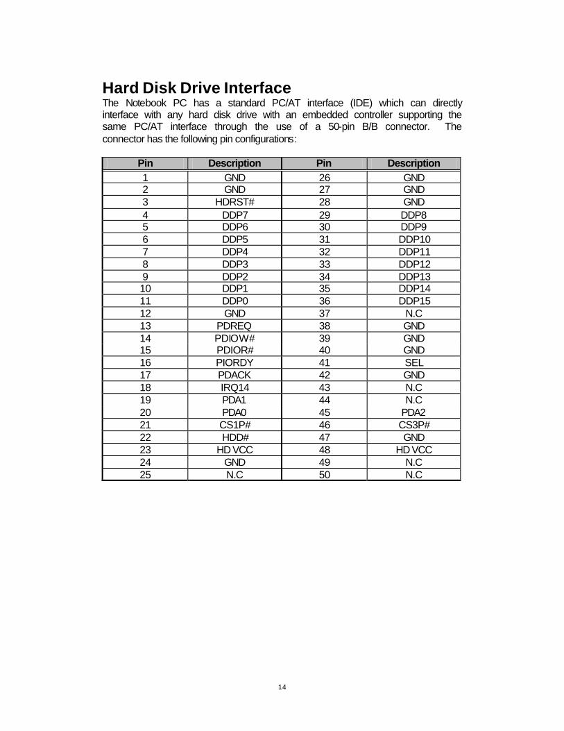
Hard Disk Drive Interface The Notebook PC has a standard PC/AT interface (IDE) which can directly interface with any hard disk drive with an embedded controller supporting the same PC/AT interface through the use of a 50-pin B/B connector. The connector has the following pin configurations:
Pin Description Pin Description 1 GND 26 GND 2 GND 27 GND 3 HDRST# 28 GND 4 DDP7 29 DDP8 5 DDP6 30 DDP9 6 DDP5 31 DDP10 7 DDP4 32 DDP11 8 DDP3 33 DDP12 9 DDP2 34 DDP13 10 DDP1 35 DDP14 11 DDP0 36 DDP15 12 GND 37 N.C 13 PDREQ 38 GND 14 PDIOW# 39 GND 15 PDIOR# 40 GND 16 PIORDY 41 SEL 17 PDACK 42 GND 18 IRQ14 43 N.C 19 PDA1 44 N.C 20 PDA0 45 PDA2 21 CS1P# 46 CS3P# 22 HDD# 47 GND 23 HD VCC 48 HD VCC 24 GND 49 N.C 25 N.C 50 N.C
15
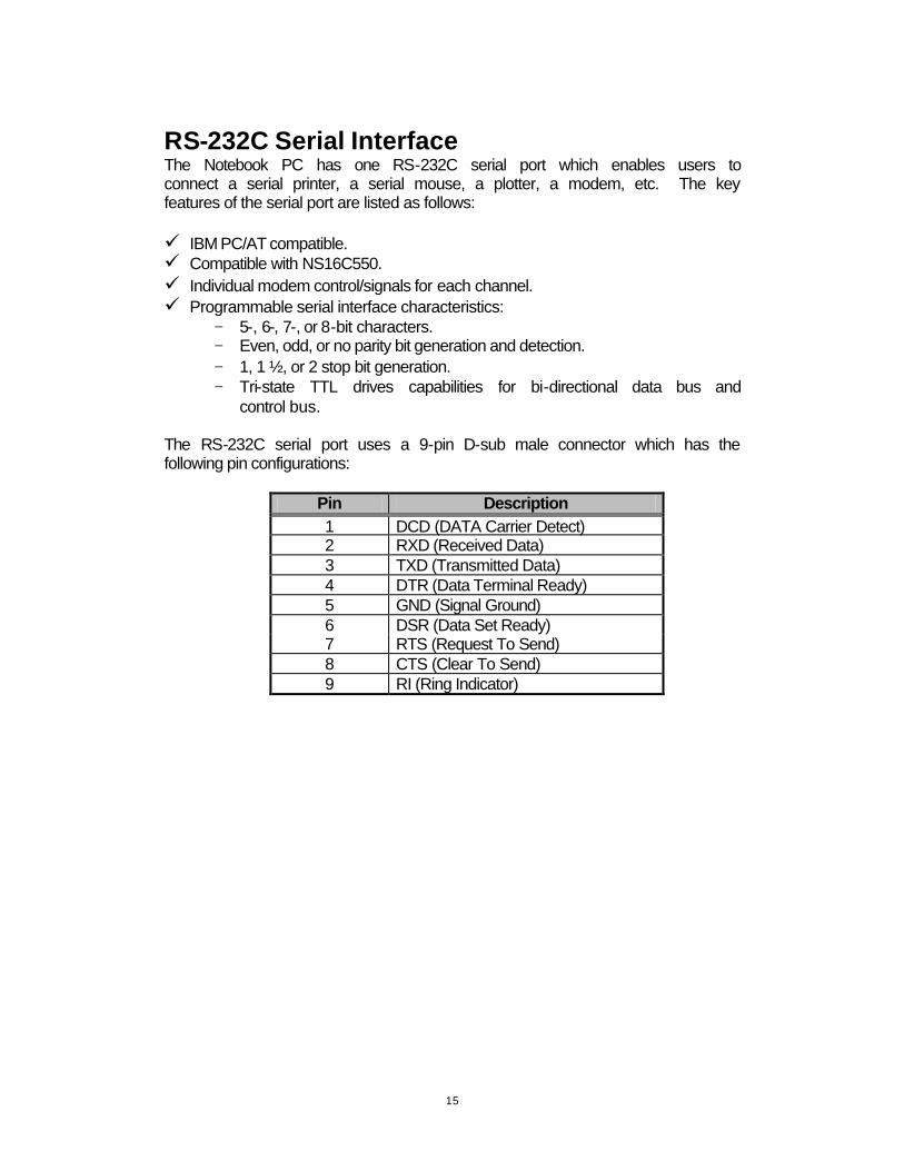
RS-232C Serial Interface The Notebook PC has one RS-232C serial port which enables users to connect a serial printer, a serial mouse, a plotter, a modem, etc. The key features of the serial port are listed as follows: ü IBM PC/AT compatible. ü Compatible with NS16C550. ü Individual modem control/signals for each channel. ü Programmable serial interface characteristics:
− 5-, 6-, 7-, or 8-bit characters. − Even, odd, or no parity bit generation and detection. − 1, 1 ½, or 2 stop bit generation. − Tri-state TTL drives capabilities for bi-directional data bus and
control bus. The RS-232C serial port uses a 9-pin D-sub male connector which has the following pin configurations:
Pin Description 1 DCD (DATA Carrier Detect) 2 RXD (Received Data) 3 TXD (Transmitted Data) 4 DTR (Data Terminal Ready) 5 GND (Signal Ground) 6 DSR (Data Set Ready) 7 RTS (Request To Send) 8 CTS (Clear To Send) 9 RI (Ring Indicator)
16
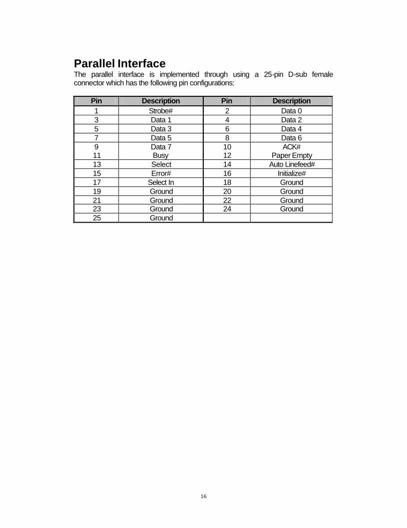
Parallel Interface The parallel interface is implemented through using a 25-pin D-sub female connector which has the following pin configurations:
Pin Description Pin Description 1 Strobe# 2 Data 0 3 Data 1 4 Data 2 5 Data 3 6 Data 4 7 Data 5 8 Data 6 9 Data 7 10 ACK# 11 Busy 12 Paper Empty 13 Select 14 Auto Linefeed# 15 Error# 16 Initialize# 17 Select In 18 Ground 19 Ground 20 Ground 21 Ground 22 Ground 23 Ground 24 Ground 25 Ground
17
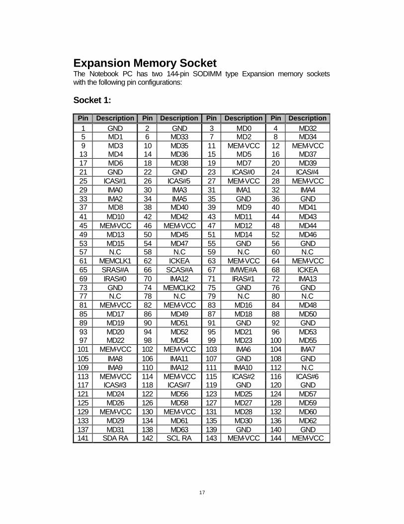
Expansion Memory Socket The Notebook PC has two 144-pin SODIMM type Expansion memory sockets with the following pin configurations: Socket 1:
Pin Description Pin Description Pin Description Pin Description
1 GND 2 GND 3 MD0 4 MD32 5 MD1 6 MD33 7 MD2 8 MD34 9 MD3 10 MD35 11 MEM-VCC 12 MEM-VCC 13 MD4 14 MD36 15 MD5 16 MD37 17 MD6 18 MD38 19 MD7 20 MD39 21 GND 22 GND 23 ICAS#0 24 ICAS#4 25 ICAS#1 26 ICAS#5 27 MEM-VCC 28 MEM-VCC 29 IMA0 30 IMA3 31 IMA1 32 IMA4 33 IMA2 34 IMA5 35 GND 36 GND 37 MD8 38 MD40 39 MD9 40 MD41 41 MD10 42 MD42 43 MD11 44 MD43 45 MEM-VCC 46 MEM-VCC 47 MD12 48 MD44 49 MD13 50 MD45 51 MD14 52 MD46 53 MD15 54 MD47 55 GND 56 GND 57 N.C 58 N.C 59 N.C 60 N.C 61 MEMCLK1 62 ICKEA 63 MEM-VCC 64 MEM-VCC 65 SRAS#A 66 SCAS#A 67 IMWE#A 68 ICKEA 69 IRAS#0 70 IMA12 71 IRAS#1 72 IMA13 73 GND 74 MEMCLK2 75 GND 76 GND 77 N.C 78 N.C 79 N.C 80 N.C 81 MEM-VCC 82 MEM-VCC 83 MD16 84 MD48 85 MD17 86 MD49 87 MD18 88 MD50 89 MD19 90 MD51 91 GND 92 GND 93 MD20 94 MD52 95 MD21 96 MD53 97 MD22 98 MD54 99 MD23 100 MD55 101 MEM-VCC 102 MEM-VCC 103 IMA6 104 IMA7 105 IMA8 106 IMA11 107 GND 108 GND 109 IMA9 110 IMA12 111 IMA10 112 N.C 113 MEM-VCC 114 MEM-VCC 115 ICAS#2 116 ICAS#6 117 ICAS#3 118 ICAS#7 119 GND 120 GND 121 MD24 122 MD56 123 MD25 124 MD57 125 MD26 126 MD58 127 MD27 128 MD59 129 MEM-VCC 130 MEM-VCC 131 MD28 132 MD60 133 MD29 134 MD61 135 MD30 136 MD62 137 MD31 138 MD63 139 GND 140 GND 141 SDA RA 142 SCL RA 143 MEM-VCC 144 MEM-VCC
18
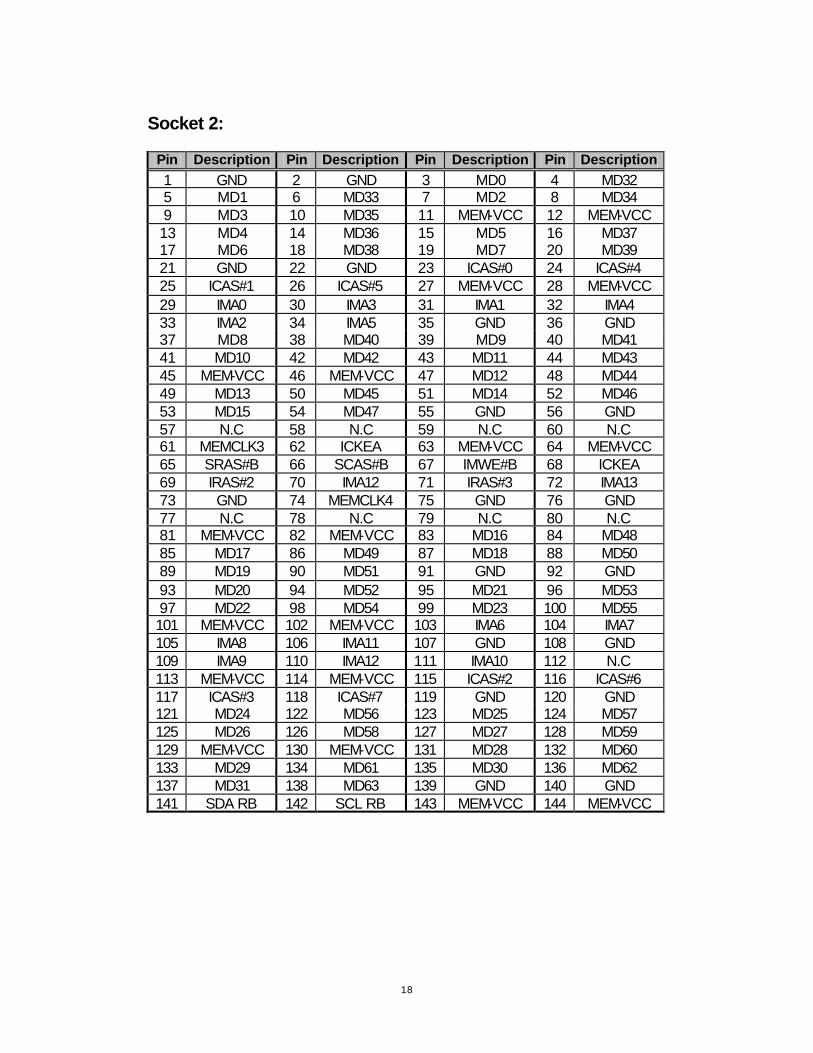
Socket 2:
Pin Description Pin Description Pin Description Pin Description
1 GND 2 GND 3 MD0 4 MD32 5 MD1 6 MD33 7 MD2 8 MD34 9 MD3 10 MD35 11 MEM-VCC 12 MEM-VCC 13 MD4 14 MD36 15 MD5 16 MD37 17 MD6 18 MD38 19 MD7 20 MD39 21 GND 22 GND 23 ICAS#0 24 ICAS#4 25 ICAS#1 26 ICAS#5 27 MEM-VCC 28 MEM-VCC 29 IMA0 30 IMA3 31 IMA1 32 IMA4 33 IMA2 34 IMA5 35 GND 36 GND 37 MD8 38 MD40 39 MD9 40 MD41 41 MD10 42 MD42 43 MD11 44 MD43 45 MEM-VCC 46 MEM-VCC 47 MD12 48 MD44 49 MD13 50 MD45 51 MD14 52 MD46 53 MD15 54 MD47 55 GND 56 GND 57 N.C 58 N.C 59 N.C 60 N.C 61 MEMCLK3 62 ICKEA 63 MEM-VCC 64 MEM-VCC 65 SRAS#B 66 SCAS#B 67 IMWE#B 68 ICKEA 69 IRAS#2 70 IMA12 71 IRAS#3 72 IMA13 73 GND 74 MEMCLK4 75 GND 76 GND 77 N.C 78 N.C 79 N.C 80 N.C 81 MEM-VCC 82 MEM-VCC 83 MD16 84 MD48 85 MD17 86 MD49 87 MD18 88 MD50 89 MD19 90 MD51 91 GND 92 GND 93 MD20 94 MD52 95 MD21 96 MD53 97 MD22 98 MD54 99 MD23 100 MD55 101 MEM-VCC 102 MEM-VCC 103 IMA6 104 IMA7 105 IMA8 106 IMA11 107 GND 108 GND 109 IMA9 110 IMA12 111 IMA10 112 N.C 113 MEM-VCC 114 MEM-VCC 115 ICAS#2 116 ICAS#6 117 ICAS#3 118 ICAS#7 119 GND 120 GND 121 MD24 122 MD56 123 MD25 124 MD57 125 MD26 126 MD58 127 MD27 128 MD59 129 MEM-VCC 130 MEM-VCC 131 MD28 132 MD60 133 MD29 134 MD61 135 MD30 136 MD62 137 MD31 138 MD63 139 GND 140 GND 141 SDA RB 142 SCL RB 143 MEM-VCC 144 MEM-VCC
19
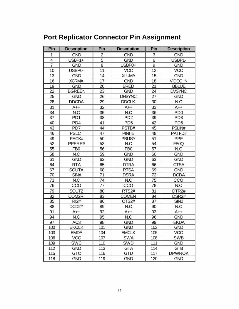
Port Replicator Connector Pin Assignment
Pin Description Pin Description Pin Description 1 GND 2 GND 3 GND 4 USBP1+ 5 GND 6 USBP1- 7 GND 8 USBP0+ 9 GND 10 USBP0- 11 VCC 12 VCC 13 GND 14 XLUMA 15 GND 16 XCRMA 17 GND 18 VIDEO IN 19 GND 20 BRED 21 BBLUE 22 BGREEN 23 GND 24 DVSYNC 25 GND 26 DHSYNC 27 GND 28 DDCDA 29 DDCLK 30 N.C 31 A++ 32 A++ 33 A++ 34 N.C 35 N.C 36 PD0 37 PD1 38 PD2 39 PD3 40 PD4 41 PD5 42 PD6 43 PD7 44 PSTB# 45 PSLIN# 46 PSLCT 47 PINIT# 48 PATFD# 49 PACK# 50 PBUSY 51 PPE 52 PPERR# 53 N.C 54 FB0Q 55 FB0 56 FB0 57 N.C 58 N.C 59 GND 60 GND 61 GND 62 GND 63 GND 64 RTA 65 DTRA 66 CTSA 67 SOUTA 68 RTSA 69 GND 70 SINA 71 DSRA 72 DCDA 73 N.C 74 N.C 75 CCO 76 CCO 77 CCO 78 N.C 79 SOUT2 80 RTS2# 81 DTR2# 82 COM2RI 83 COMEN 84 DSR2# 85 RI2# 86 CTS2# 87 SIN2 88 DCD2# 89 N.C 90 N.C 91 A++ 92 A++ 93 A++ 94 N.C 95 N.C 96 GND 97 AC3 98 GND 99 EKDA 100 EKCLK 101 GND 102 GND 103 EMDA 104 EMCLK 105 VCC 106 VCC 107 SWA 108 SWB 109 SWC 110 SWD 111 GND 112 GND 113 GTA 114 GTB 115 GTC 116 GTD 117 DPWROK 118 GND 119 GND 120 GND
20
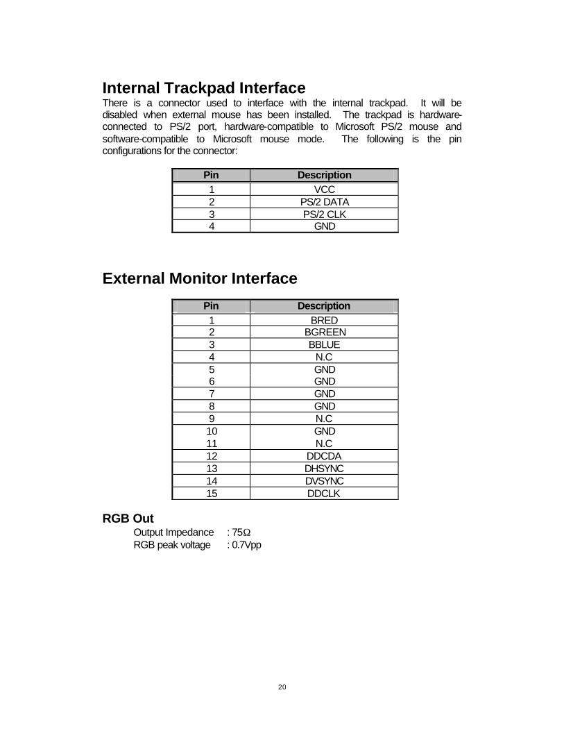
Internal Trackpad Interface There is a connector used to interface with the internal trackpad. It will be disabled when external mouse has been installed. The trackpad is hardware-connected to PS/2 port, hardware-compatible to Microsoft PS/2 mouse and software-compatible to Microsoft mouse mode. The following is the pin configurations for the connector:
Pin Description 1 VCC 2 PS/2 DATA 3 PS/2 CLK 4 GND
External Monitor Interface
Pin Description 1 BRED 2 BGREEN 3 BBLUE 4 N.C 5 GND 6 GND 7 GND 8 GND 9 N.C 10 GND 11 N.C 12 DDCDA 13 DHSYNC 14 DVSYNC 15 DDCLK
RGB Out Output Impedance : 75Ω RGB peak voltage : 0.7Vpp
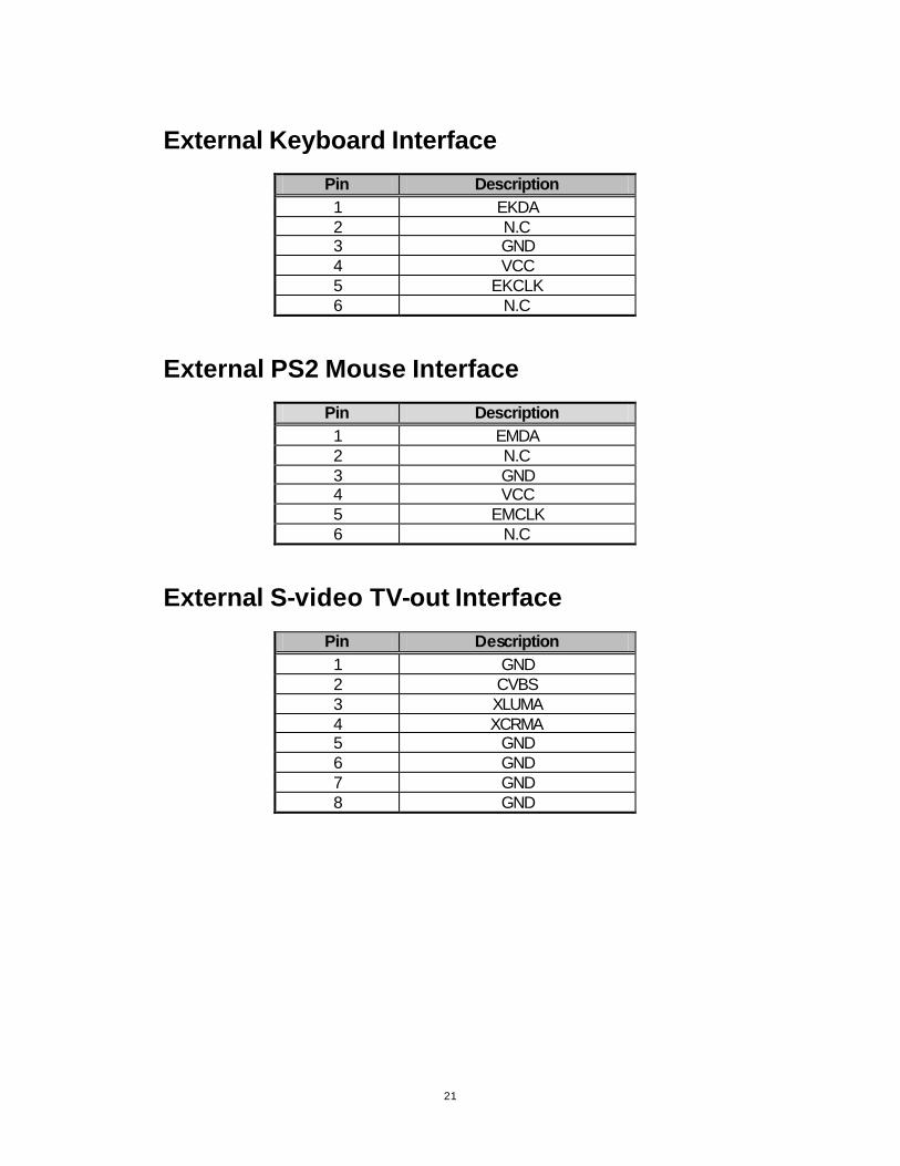
21
External Keyboard Interface
Pin Description 1 EKDA 2 N.C 3 GND 4 VCC 5 EKCLK 6 N.C
External PS2 Mouse Interface
Pin Description 1 EMDA 2 N.C 3 GND 4 VCC 5 EMCLK 6 N.C
External S-video TV-out Interface
Pin Description 1 GND 2 CVBS 3 XLUMA 4 XCRMA 5 GND 6 GND 7 GND 8 GND

22
Video-in Interface
Pin Description 1 Video-in 2 GND
External USB (Universal Serial Bus) Interface Port A:
Pin Description 1 USB VCCA 2 USBP0- 3 USBP0+ 4 GND
Port B:
Pin Description 1 USB VCCB 2 USBP1- 3 USBP1+ 4 GND
23
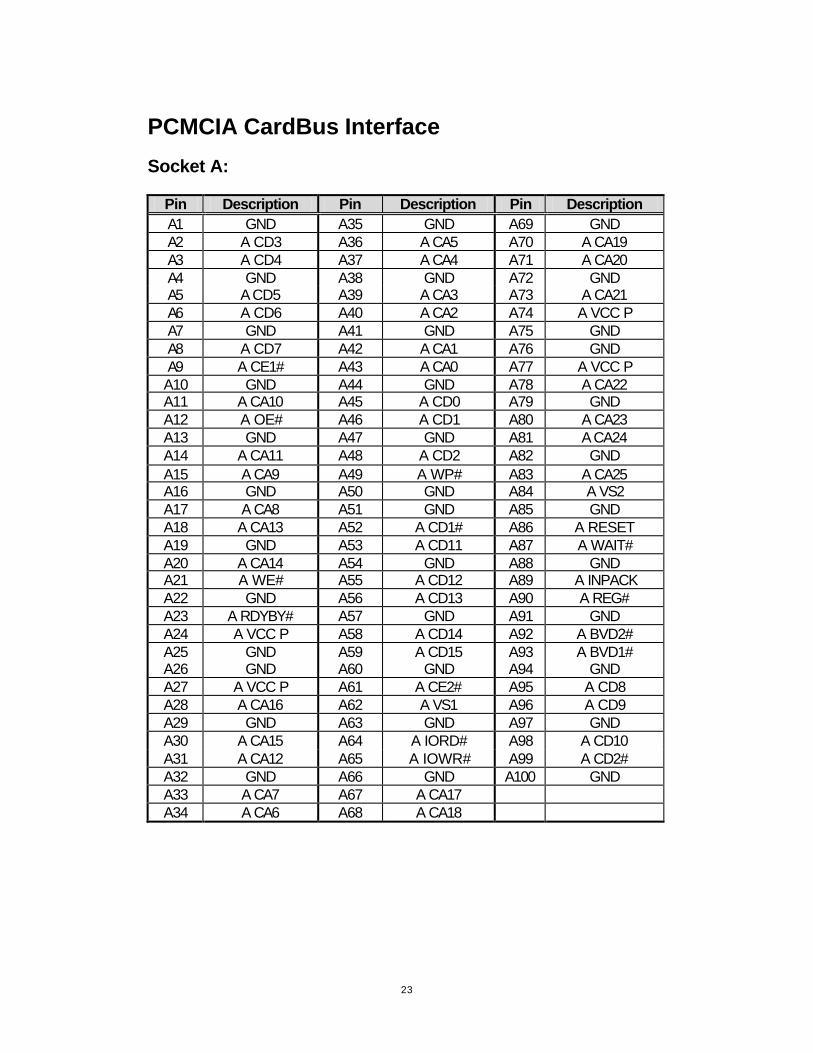
PCMCIA CardBus Interface Socket A:
Pin Description Pin Description Pin Description A1 GND A35 GND A69 GND A2 A CD3 A36 A CA5 A70 A CA19 A3 A CD4 A37 A CA4 A71 A CA20 A4 GND A38 GND A72 GND A5 A CD5 A39 A CA3 A73 A CA21 A6 A CD6 A40 A CA2 A74 A VCC P A7 GND A41 GND A75 GND A8 A CD7 A42 A CA1 A76 GND A9 A CE1# A43 A CA0 A77 A VCC P A10 GND A44 GND A78 A CA22 A11 A CA10 A45 A CD0 A79 GND A12 A OE# A46 A CD1 A80 A CA23 A13 GND A47 GND A81 A CA24 A14 A CA11 A48 A CD2 A82 GND A15 A CA9 A49 A WP# A83 A CA25 A16 GND A50 GND A84 A VS2 A17 A CA8 A51 GND A85 GND A18 A CA13 A52 A CD1# A86 A RESET A19 GND A53 A CD11 A87 A WAIT# A20 A CA14 A54 GND A88 GND A21 A WE# A55 A CD12 A89 A INPACK A22 GND A56 A CD13 A90 A REG# A23 A RDYBY# A57 GND A91 GND A24 A VCC P A58 A CD14 A92 A BVD2# A25 GND A59 A CD15 A93 A BVD1# A26 GND A60 GND A94 GND A27 A VCC P A61 A CE2# A95 A CD8 A28 A CA16 A62 A VS1 A96 A CD9 A29 GND A63 GND A97 GND A30 A CA15 A64 A IORD# A98 A CD10 A31 A CA12 A65 A IOWR# A99 A CD2# A32 GND A66 GND A100 GND A33 A CA7 A67 A CA17 A34 A CA6 A68 A CA18
24
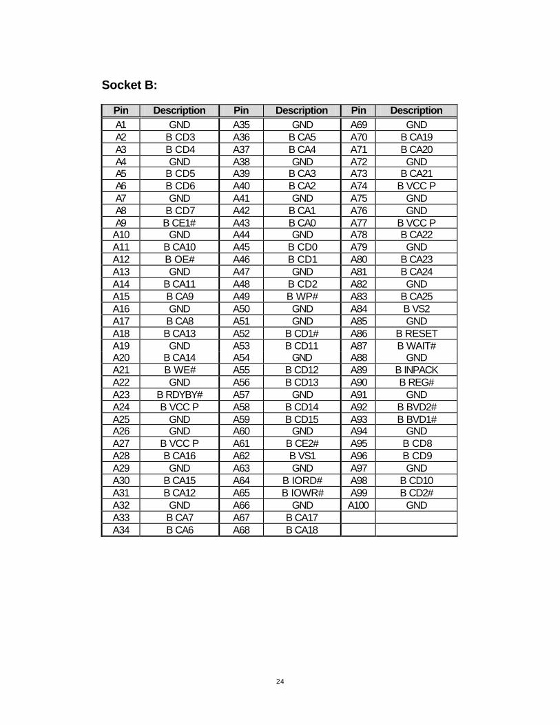
Socket B:
Pin Description Pin Description Pin Description A1 GND A35 GND A69 GND A2 B CD3 A36 B CA5 A70 B CA19 A3 B CD4 A37 B CA4 A71 B CA20 A4 GND A38 GND A72 GND A5 B CD5 A39 B CA3 A73 B CA21 A6 B CD6 A40 B CA2 A74 B VCC P A7 GND A41 GND A75 GND A8 B CD7 A42 B CA1 A76 GND A9 B CE1# A43 B CA0 A77 B VCC P A10 GND A44 GND A78 B CA22 A11 B CA10 A45 B CD0 A79 GND A12 B OE# A46 B CD1 A80 B CA23 A13 GND A47 GND A81 B CA24 A14 B CA11 A48 B CD2 A82 GND A15 B CA9 A49 B WP# A83 B CA25 A16 GND A50 GND A84 B VS2 A17 B CA8 A51 GND A85 GND A18 B CA13 A52 B CD1# A86 B RESET A19 GND A53 B CD11 A87 B WAIT# A20 B CA14 A54 GND A88 GND A21 B WE# A55 B CD12 A89 B INPACK A22 GND A56 B CD13 A90 B REG# A23 B RDYBY# A57 GND A91 GND A24 B VCC P A58 B CD14 A92 B BVD2# A25 GND A59 B CD15 A93 B BVD1# A26 GND A60 GND A94 GND A27 B VCC P A61 B CE2# A95 B CD8 A28 B CA16 A62 B VS1 A96 B CD9 A29 GND A63 GND A97 GND A30 B CA15 A64 B IORD# A98 B CD10 A31 B CA12 A65 B IOWR# A99 B CD2# A32 GND A66 GND A100 GND A33 B CA7 A67 B CA17 A34 B CA6 A68 B CA18
25
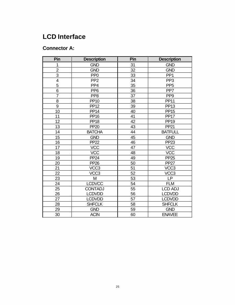
LCD Interface Connector A:
Pin Description Pin Description 1 GND 31 GND 2 GND 32 GND 3 PP0 33 PP1 4 PP2 34 PP3 5 PP4 35 PP5 6 PP6 36 PP7 7 PP8 37 PP9 8 PP10 38 PP11 9 PP12 39 PP13 10 PP14 40 PP15 11 PP16 41 PP17 12 PP18 42 PP19 13 PP20 43 PP21 14 BATCHA 44 BATFULL 15 GND 45 GND 16 PP22 46 PP23 17 VCC 47 VCC 18 VCC 48 VCC 19 PP24 49 PP25 20 PP26 50 PP27 21 VCC3 51 VCC3 22 VCC3 52 VCC3 23 M 53 LP 24 LCDVCC 54 FLM 25 CONTADJ 55 LCD ADJ 26 LCDVDD 56 LCDVDD 27 LCDVDD 57 LCDVDD 28 SHFCLK 58 SHFCLK 29 GND 59 GND 30 ACIN 60 ENAVEE
26
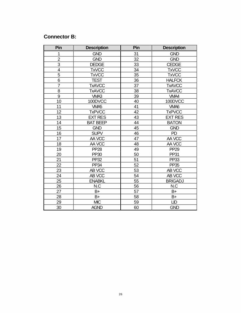
Connector B:
Pin Description Pin Description 1 GND 31 GND 2 GND 32 GND 3 DEDGE 33 CEDGE 4 TxVCC 34 TxVCC 5 TxVCC 35 TxVCC 6 TEST 36 HALFCK 7 TxAVCC 37 TxAVCC 8 TxAVCC 38 TxAVCC 9 VMA3 39 VMA4 10 100DVCC 40 100DVCC 11 VMA5 41 VMA6 12 TxPVCC 42 TxPVCC 13 EXT RES 43 EXT RES 14 BAT BEEP 44 BATON 15 GND 45 GND 16 SUPV 46 PD 17 AA VCC 47 AA VCC 18 AA VCC 48 AA VCC 19 PP28 49 PP29 20 PP30 50 PP31 21 PP32 51 PP33 22 PP34 52 PP35 23 AB VCC 53 AB VCC 24 AB VCC 54 AB VCC 25 ENABKL 55 BRIGADJ 26 N.C 56 N.C 27 B+ 57 B+ 28 B+ 58 B+ 29 MIC 59 LID 30 AGND 60 GND

27
Internal ISA Interface (for Optional Modem/LAN)
Pin Description Pin Description 1 RSTDRV 31 MODEM 2 SD0 32 SD1 3 SD2 33 SD3 4 SD4 34 SD5 5 SD6 35 SD7 6 N.C 36 AGND 7 VCCS 37 AUXBR 8 VCCS 38 AGND 9 VCCS 39 VCCA 10 AGND 40 VCCA 11 MIC IN 41 N.C 12 AGND 42 +12V 13 IORD# 43 AEN 14 IOWR# 44 IRQ10 15 IRQ3 45 IRQ11 16 IRQ4 46 IRQ12 17 IRQ5 47 GND 18 IRQ9 48 OSC4 19 SA0 49 SA1 20 SA2 50 SA3 21 SA4 51 SA5 22 SA6 52 SA7 23 SA8 53 SA9 24 SA10 54 SA11 25 SA12 55 SA13 26 SA14 56 SA15 27 GND 57 GND 28 N.C 58 N.C 29 N.C 59 N.C 30 N.C 60 N.C
28
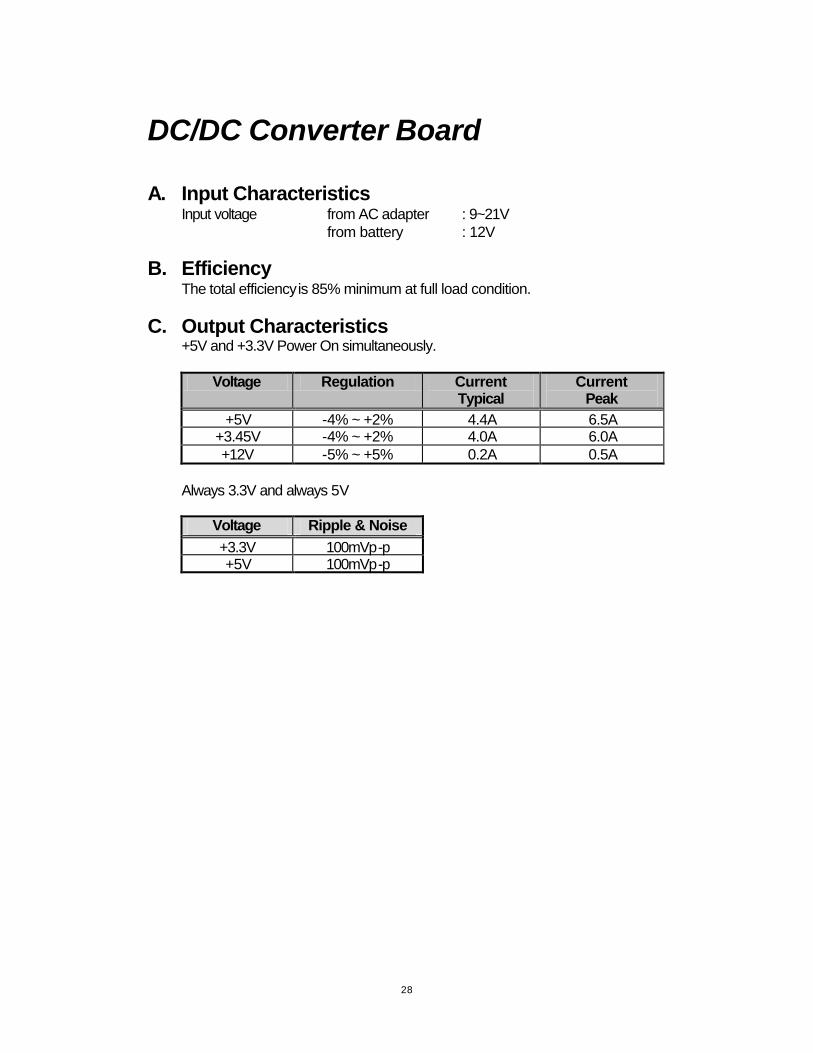
DC/DC Converter Board A. Input Characteristics
Input voltage from AC adapter : 9~21V from battery : 12V
B. Efficiency
The total efficiency is 85% minimum at full load condition. C. Output Characteristics
+5V and +3.3V Power On simultaneously.
Voltage Regulation Current Typical
Current Peak
+5V -4% ~ +2% 4.4A 6.5A +3.45V -4% ~ +2% 4.0A 6.0A +12V -5% ~ +5% 0.2A 0.5A
Always 3.3V and always 5V
Voltage Ripple & Noise
+3.3V 100mVp-p +5V 100mVp-p
29
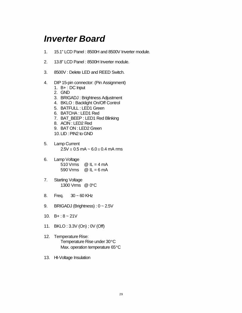
Inverter Board 1. 15.1” LCD Panel : 8500H and 8500V Inverter module. 2. 13.8” LCD Panel : 8500H Inverter module. 3. 8500V : Delete LED and REED Switch.
4. DIP 15-pin connector: (Pin Assignment)
1. B+ : DC Input 2. GND 3. BRIGADJ : Brightness Adjustment 4. BKLO : Backlight On/Off Control 5. BATFULL : LED1 Green 6. BATCHA : LED1 Red 7. BAT_BEEP : LED1 Red Blinking 8. ACIN : LED2 Red 9. BAT ON : LED2 Green 10. LID : PIN2 to GND
5. Lamp Current 2.5V ± 0.5 mA ~ 6.0 ± 0.4 mA rms
6. Lamp Voltage 510 Vrms @ IL = 4 mA 590 Vrms @ IL = 6 mA
7. Starting Voltage 1300 Vrms @ 0°C
8. Freq. 30 ~ 60 KHz 9. BRIGADJ (Brightness) : 0 ~ 2.5V 10. B+ : 8 ~ 21V 11. BKLO : 3.3V (On) ; 0V (Off) 12. Temperature Rise:
Temperature Rise under 30°C Max. operation temperature 65°C
13. HI-Voltage Insulation
30
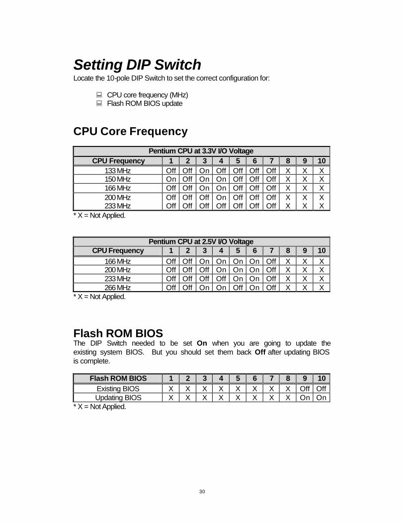
Setting DIP Switch Locate the 10-pole DIP Switch to set the correct configuration for:
: CPU core frequency (MHz) : Flash ROM BIOS update
CPU Core Frequency
Pentium CPU at 3.3V I/O Voltage CPU Frequency 1 2 3 4 5 6 7 8 9 10
133 MHz Off Off On Off Off Off Off X X X 150 MHz On Off On On Off Off Off X X X 166 MHz Off Off On On Off Off Off X X X 200 MHz Off Off Off On Off Off Off X X X 233 MHz Off Off Off Off Off Off Off X X X
* X = Not Applied.
Pentium CPU at 2.5V I/O Voltage CPU Frequency 1 2 3 4 5 6 7 8 9 10
166 MHz Off Off On On On On Off X X X 200 MHz Off Off Off On On On Off X X X 233 MHz Off Off Off Off On On Off X X X 266 MHz Off Off On On Off On Off X X X
* X = Not Applied.
Flash ROM BIOS The DIP Switch needed to be set On when you are going to update the existing system BIOS. But you should set them back Off after updating BIOS is complete.
Flash ROM BIOS 1 2 3 4 5 6 7 8 9 10 Existing BIOS X X X X X X X X Off Off Updating BIOS X X X X X X X X On On
* X = Not Applied.
31
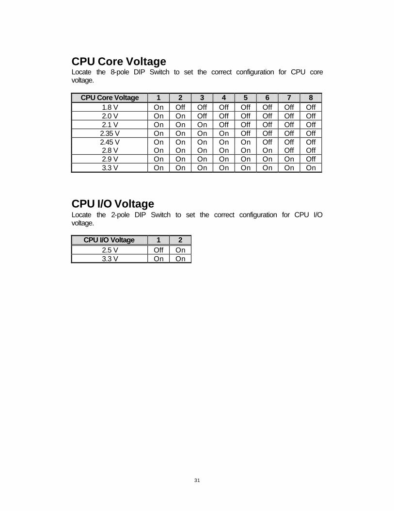
CPU Core Voltage Locate the 8-pole DIP Switch to set the correct configuration for CPU core voltage.
CPU Core Voltage 1 2 3 4 5 6 7 8 1.8 V On Off Off Off Off Off Off Off 2.0 V On On Off Off Off Off Off Off 2.1 V On On On Off Off Off Off Off 2.35 V On On On On Off Off Off Off 2.45 V On On On On On Off Off Off 2.8 V On On On On On On Off Off 2.9 V On On On On On On On Off 3.3 V On On On On On On On On
CPU I/O Voltage Locate the 2-pole DIP Switch to set the correct configuration for CPU I/O voltage.
CPU I/O Voltage 1 2 2.5 V Off On 3.3 V On On
32
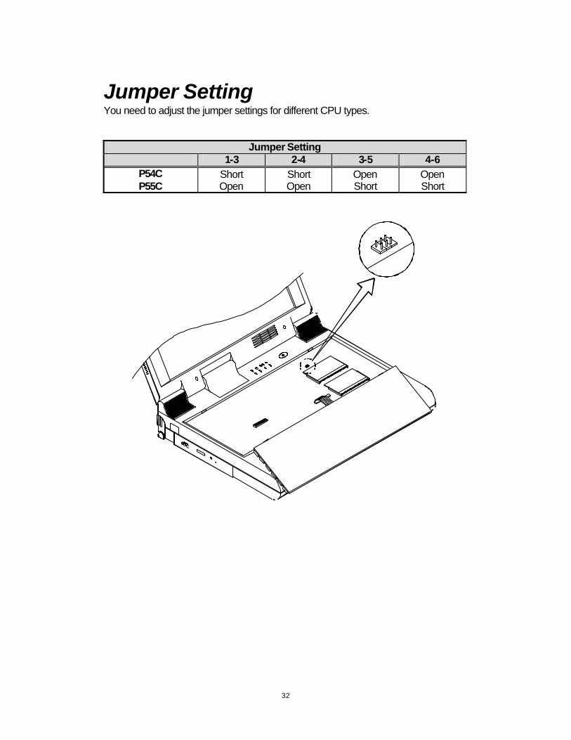
Jumper Setting You need to adjust the jumper settings for different CPU types.
Jumper Setting 1-3 2-4 3-5 4-6
P54C Short Short Open Open P55C Open Open Short Short
33
System Resource Allocation
IRQ: IRQ 0: System timer IRQ 1: Keyboard IRQ 2: Cascade to 2nd 8259 IRQ 3: COM2 IRQ 4: COM1 IRQ 5: Audio IRQ 6: Floppy IRQ 7: Printer IRQ 8: RTC alarm IRQ 9: SCI. (ACPI), PCIIRQ router (PCI interrupt) (may share with SCI) IRQ 10: Legacy PCMCIA CSC/functional interrupt, PCI router (PCI interrupt) IRQ 11: Legacy PCMCIA CSC/functional interrupt, PCI router (PCI interrupt)
or USB controller IRQ 12: PS2 mouse IRQ 13: FPU IRQ 14: Primary IDE (HDD) IRQ 15: Secondary IDE (CD-ROM/2nd HDD/LS-120/Zip/MO) DMA: DMA1, 5: Audio chip (full duplex) DMA 0: LPT (ECP mode) DMA 2: FDC DMA 3: FIR DMA 6, 7: DMA PC card of PCMCIA controller (PC/PCI DMA)

34
System Block Diagram
35
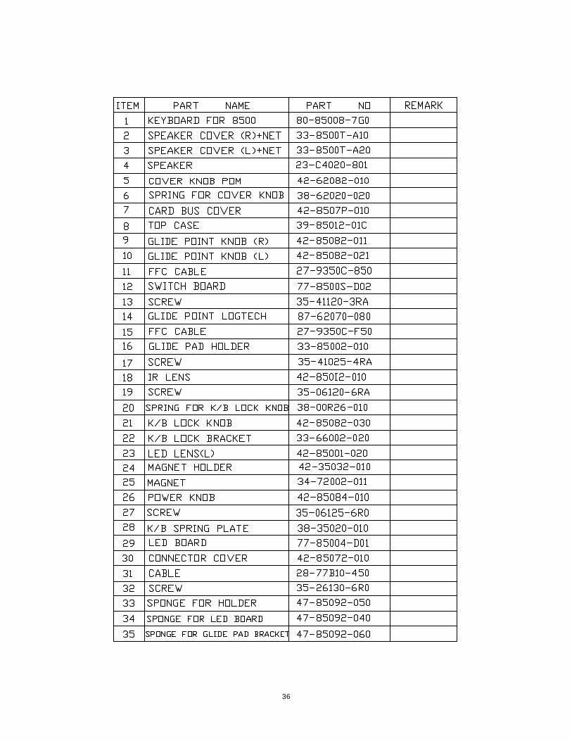
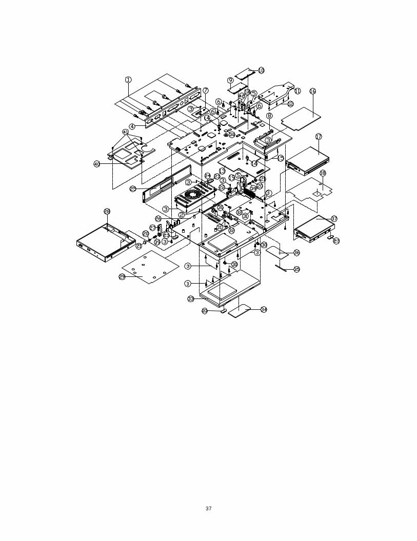
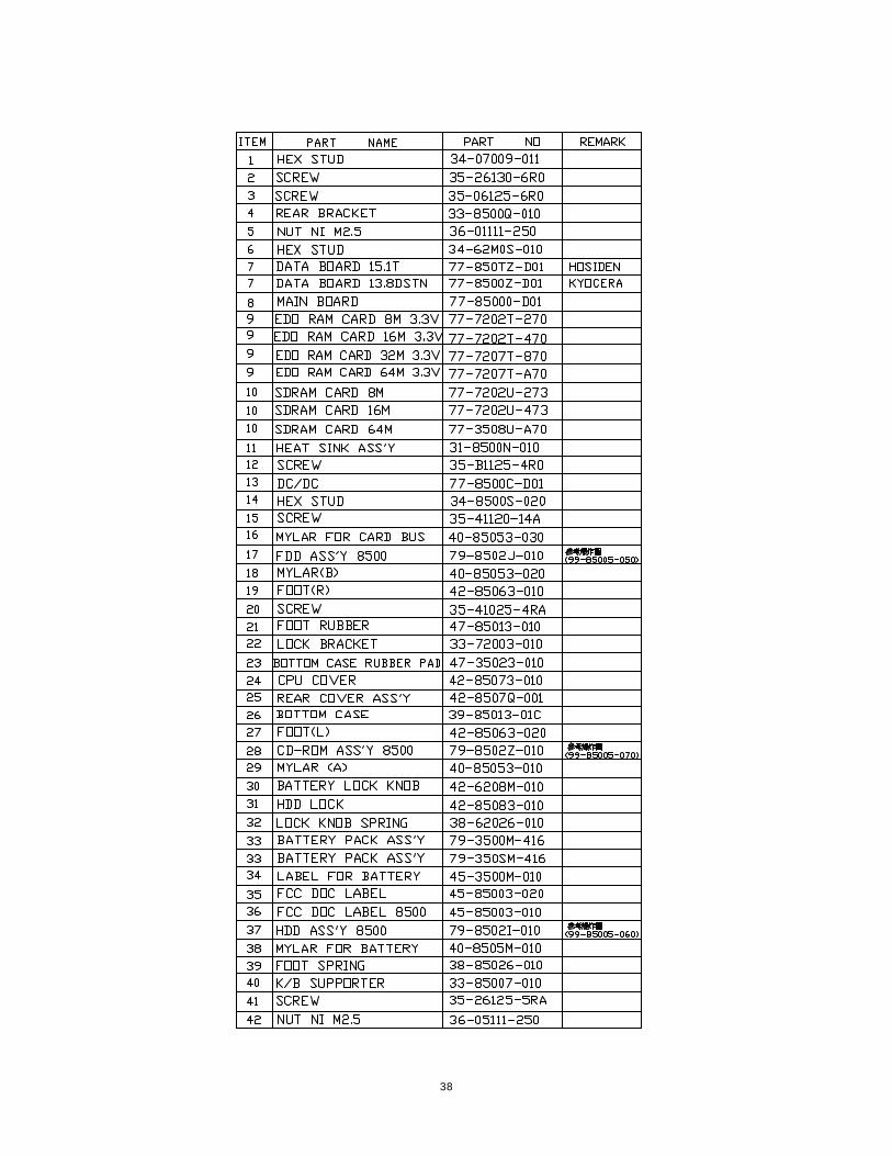
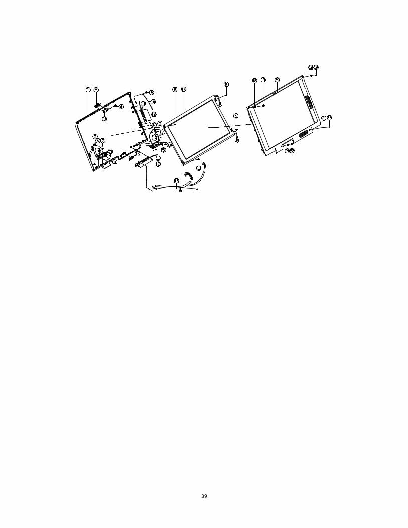
36
37
38
39
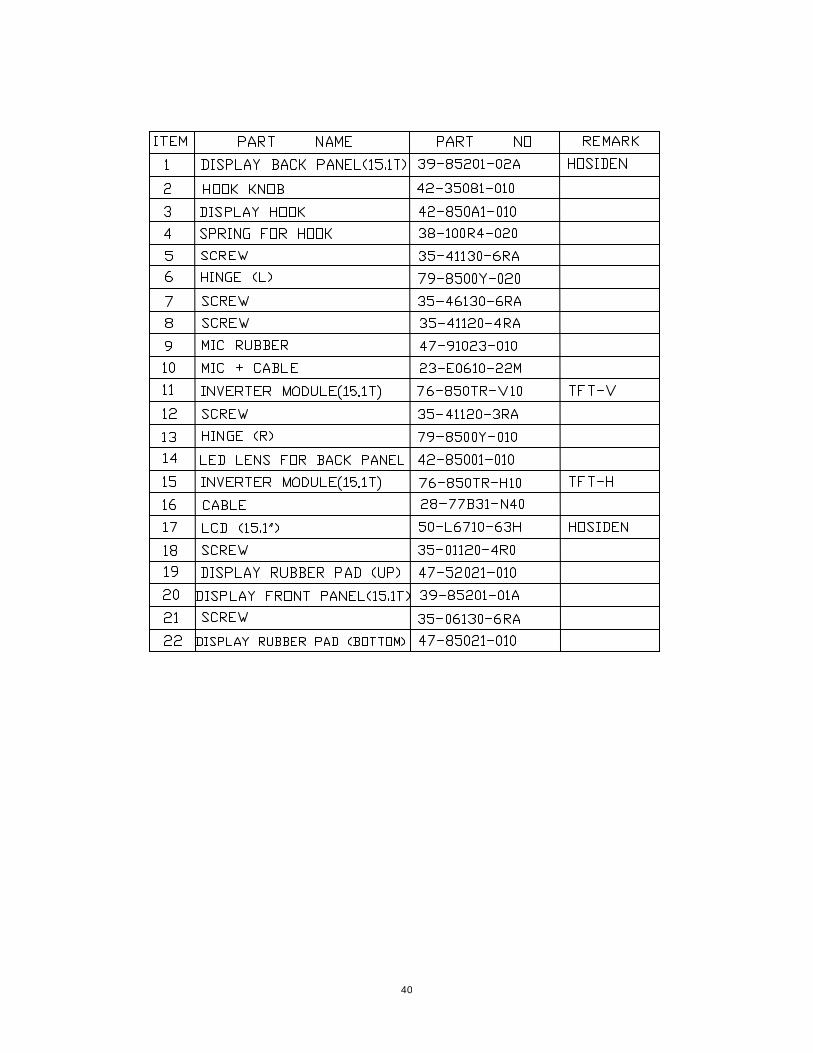
40
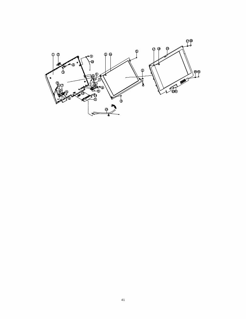
41

42

43
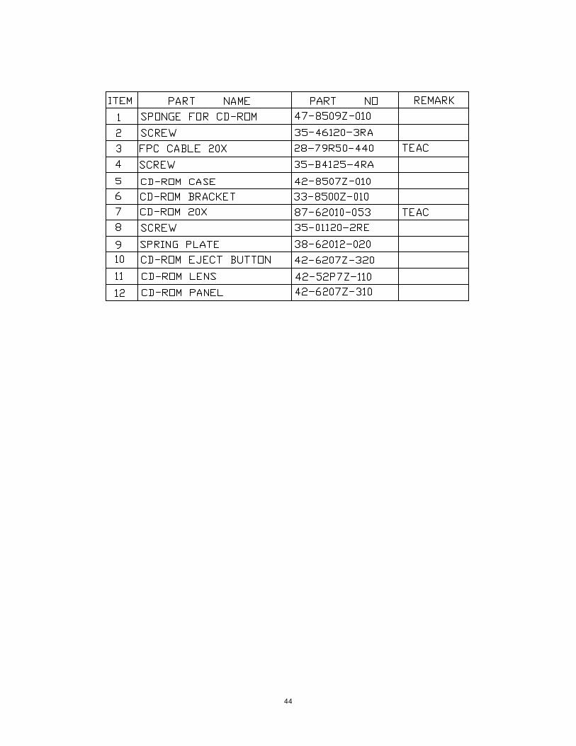
44
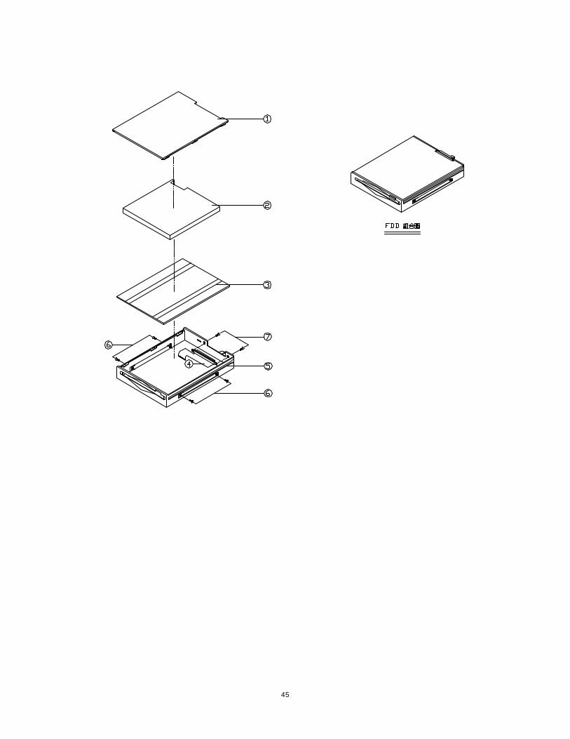
45

46
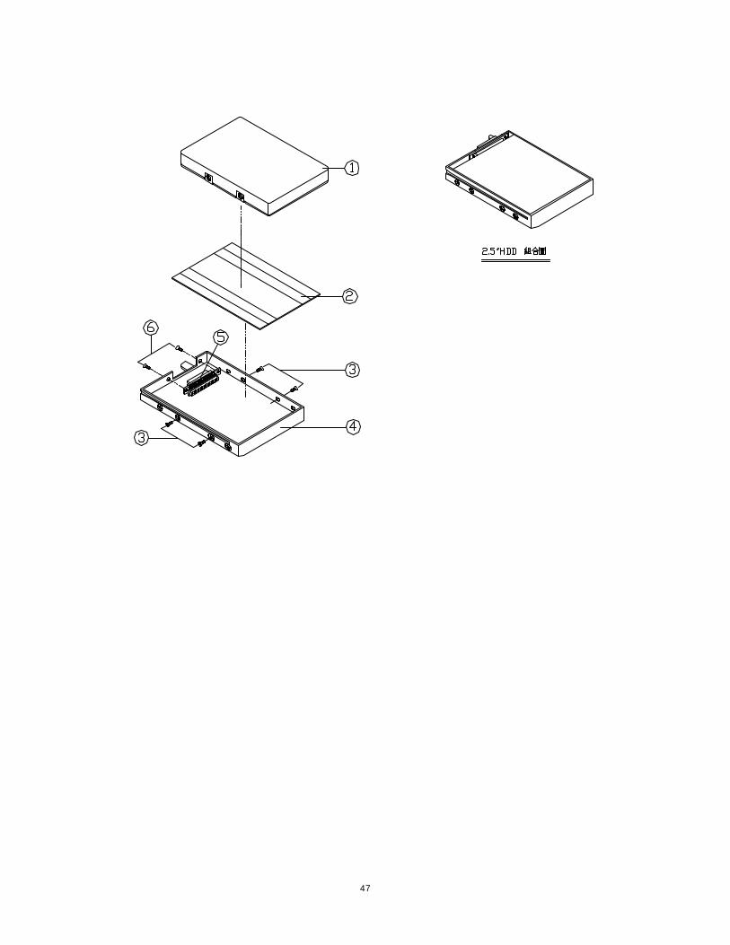
47

48