Embed Size (px)
Citation preview

Data Sheetwww.lumentum.com
8.5 G SFP+ 850 nm Limiting Transceiver, 8 Gigabit Fibre Channel CompliantPLRXPL-Vx-SH4-23-N Series
8.5 G SFP+ 850 nm Limiting Transceiver, 8 Gigabit Fibre Channel Compliant
www.lumentum.com 2
The lead-free and RoHS-compliant small form factor pluggable (SFP+) transceiver from Lumentum improves the performance for 8 Gigabit Fibre Channel (8GFC) applications, and is ideal for high-speed, storage area network applications. This transceiver features a highly reliable, 850 nm, oxide, vertical-cavity surface-emitting laser (VCSEL) coupled to an LC optical connector. The transceiver is fully compliant to the FC-PI-4, and the SFP+ specifications at 8.5 G, 4.25 G and 2.125 G bit rates, with internal AC coupling on both transmit and receive data signals. The all-metal housing design provides low EMI emissions in demanding 8 G applications and conforms to IPF specifications. An enhanced digital diagnostic feature set allows for real-time monitoring of transceiver performance and system stability, and the serial ID allows for customer and vendor system information to be stored in the transceiver. Transmit disable, loss-of-signal, and transmitter fault functions are also provided. The small size of the transceiver allows for high-density system designs that, in turn, enable greater total bandwidth.
Key Features• Compliant to industry-wide, 8 G Fibre Channel (FC)
link specifications
• Maintains FC compliance at 4 and 2 G without need for a rate select option
• Uses a highly reliable, 850 nm oxide VCSEL
• Lead-free and RoHS 6/6-compliant, with allowed exemptions
• Commercial case operating temperature of 0 – 70°C; extended temperature operation up to 85°C
• Single 3.3 V power supply
• Low power consumption (typically 450 mW)
• Bit error rate < 1 x 10-12
• 6G OBSAI/CPRI compliant
Applications• High-speed storage area networks
− Switches and hubs
− Network interface cards
− Mass storage systems
− Host bus adapters
• Computer cluster crossconnect systems
• Wireless backhaul
Compliance• SFF 8431 Revision 3.2
• SFF 8432 Revision 5.0
• SFF 8472 Revision 10.3
• CPRI Version 4.1
• OBSAI RP3-01
• FCC Class B
• ESD Class 2 per MIL-STD 883 Method 3015
• UL 94, V0
• Reliability tested per Telcordia GR-468

8.5 G SFP+ 850 nm Limiting Transceiver, 8 Gigabit Fibre Channel Compliant
www.lumentum.com 3
Section 1 Functional Description
The PLRXPL-Vx-SH4-23-N 8.5 G SFP+ 850 nm optical transceiver is designed to transmit and receive 8B/10B scrambled 8.5 G serial optical data over 50/125 µm or 62.5/125 µm multimode optical fiber.
TransmitterThe transmitter converts 8B/10B scrambled serial PECL or CML electrical data into serial optical data compliant with the 8 G Fibre Channel standard. Transmit data lines (TD+ and TD-) are internally AC coupled, with 100 Ω differential termination.
Transmitter rate select (RS1) pin 9 is assigned to control the SFP+ module transmitter rate. It is connected internally to a 30 kΩ pull-down resistor. A data signal on this pin does not affect the operation of the transmitter.
An open collector-compatible transmit disable (Tx_Disable) is provided. This pin is internally terminated with a 10 kΩ resistor to Vcc,T. A logic “1,” or no connection, on this pin will disable the laser from transmitting. A logic “0” on this pin provides normal operation.
The transmitter has an internal PIN monitor diode that ensures constant optical power output, independent of supply voltage. It is also used to control the laser output power over temperature to ensure reliability at high temperatures.
An open collector-compatible transmit fault (Tx_Fault) is provided. The Tx_Fault signal must be pulled high on the host board for proper operation. A logic “1” output from this pin indicates that a transmitter fault has occurred or that the part is not fully seated and the transmitter is disabled. A logic “0” on this pin indicates normal operation.
ReceiverThe receiver converts 8B/10B scrambled serial optical data into serial PECL/CML electrical data. Receive data lines (RD+ and RD-) are internally AC coupled with 100 Ω differential source impedance, and must be terminated with a 100 Ω differential load.
Receiver Rate Select (RS0) pin 7 is assigned to control the SFP+ module receiver rate. It is connected internally to a 30 kΩ pull-down resistor. A data signal on this pin has no affect on the operation of the receiver.
An open collector compatible loss of signal (LOS) is provided. The LOS must be pulled high on the host board for proper operation. A logic “0” indicates that light has been detected at the input to the receiver (see Optical Characteristics, Loss of Signal Assert/Deassert Time). A logic “1” output indicates that insufficient light has been detected for proper operation.
Laser DriverTOSA
ROSA
Management Processor
EEPROM
Receiver
50 Ω
50 Ω
10 kΩ
100 Ω
TX_GND TX_FAULT
VCC_TX TX_DIS
SCL
SDA
TD+
TD -
RD -
RD +
RX_GND
VCC_RX VCC_RX
RX_GND
30 kΩ
LOS
16 TransmitterPower Supply
3 TransmitterDisable In
18 TransmitterPositive Data
19 TransmitterNegative Data
2 TransmitterFault Out
1, 17, 20 TransmitterSignal Ground
5 SCLSerial ID Clock4 SDASerial ID Data
6 MOD_ABS
15 ReceiverPower Supply
12 ReceiverNegative Data Out
13 ReceiverPositive Data Out
8 Loss of Signal Out
7 RS0 RX Rate SelectNot Functional on-N modules
10, 11, 14 ReceiverSignal Ground
30 kΩ
9 RS1 TX Rate SelectNot Functional on-N modules
Figure 1 SFP+ optical transceiver functional block diagram
8.5 G SFP+ 850 nm Limiting Transceiver, 8 Gigabit Fibre Channel Compliant
www.lumentum.com 4
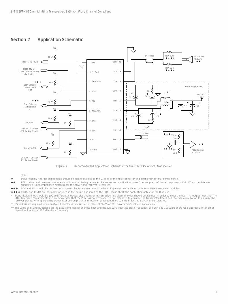
Section 2 Application Schematic
Receiver (Tx Fault)
Vcc
10 kΩ
CMOS, TTL, orOpen Collector Driver
(Tx Disable)
Open CollectorBidirectional
SDA
Vcc
Rp***
Vcc
Open CollectorBidirectional
SCL
Rq ***
Mod_ABS
10 kΩ
Vcc
1 VeeT
2 Tx Fault
3 Tx Disable
4 SDA
5 SCL
6 MOD_ABS
7 RS0
8 LOS
9 RS1
10 VeeR
VeeT 20
TD- 19
TD+ 18
VeeT 17
VccT 16
VccR 15
VeeR 14
RD+ 13
RD- 12
VeeR 11
10 kΩ
Vcc
Receiver (LOS)
R1 * 50 Ω
R2 * 50 Ω
L1
L2
Z* = 100 Ω PECL Driver(TX DATA)
C1C2
C5C4
C3
CMOS or TTL Driver(RS0 Rx Rate Select)
CMOS or TTL Driver(RS1 Tx Rate Select)
Vcc
R6 **
R5 **
Vcc
Vcc +3.3V
Input
R3 *
50 Ω
R4 *
50 Ω
PECL Receiver(RX DATA)
Z * = 100 Ω
Power Supply Filter
C6
Ry
Rx
Figure 2 Recommended application schematic for the 8 G SFP+ optical transceiver
Notes
Power supply filtering components should be placed as close to the Vcc pins of the host connector as possible for optimal performance.
PECL driver and receiver components will require biasing networks. Please consult application notes from suppliers of these components. CML I/O on the PHY are supported. Good impedance matching for the driver and receiver is required.
SDA and SCL should be bi-directional open collector connections in order to implement serial ID in Lumentum SFP+ transceiver modules.
R1/R2 and R3/R4 are normally included in the output and input of the PHY. Please check the application notes for the IC in use.
* Transmission lines should be 100 Ω differential traces. Vias and other transmission line discontinuities should be avoided. In order to meet the host TP1 output jitter and TP4 jitter tolerance requirements it is recommended that the PHY has both transmitter pre-emphasis to equalize the transmitter traces and receiver equalization to equalize the receiver traces. With appropriate transmitter pre-emphasis and receiver equalization, up to 8 dB of loss at 5 GHz can be tolerated.
** R5 and R6 are required when an Open Collector driver is used in place of CMOS or TTL drivers. 5 kΩ value is appropriate.
*** The value of Rp and Rq depend on the capacitive loading of these lines and the two wire interface clock frequency. See SFF-8431. A value of 10 kΩ is appropriate for 80 pF capacitive loading at 100 kHz clock frequency.

8.5 G SFP+ 850 nm Limiting Transceiver, 8 Gigabit Fibre Channel Compliant
www.lumentum.com 5
Power supply filtering is recommended for both the transmitter and receiver. Filtering should be placed on the host assembly as close to the Vcc pins as possible for optimal performance. Vcc,R and Vcc,T should have separate filters.
Power supply filter component values from Figure 2 are shown in the table below for two different implementations.
Power Supply Filter Component Values
Component Option A Option B Units
L1, L2 1.0 4.7 μH
Rx, Ry 0.5* 0.5* Ω
C1, C5 10 22 μF
C2, C3, C4 0.1 0.1 μF
C6 Not required 22 μF
Notes:
Option A is recommended for use in applications with space constraints. Power supply noise must be less than 100 mVp-p.
Option B is used in the module compliance board in SFF-8431.
*If the total series resistance of L1+C6 and L2+C5 exceeds the values of Rx and Ry in the table, then Rx and Ry can be omitted.
Section 3 Specifications
Technical specifications related to the SFP+ optical transceiver include:
Section 3.1 Pin Function Definitions
Section 3.2 Absolute Maximum Ratings
Section 3.3 Operating Conditions
Section 3.4 Electrical Characteristics
Section 3.5 Optical Characteristics
Section 3.6 Link Length
Section 3.7 Regulatory Compliance
Section 3.8 PCB Layout
Section 3.9 Front Panel Opening
Section 3.10 Module Outline
Section 3.11 Transceiver Belly-to-belly Mounting
3.1 Pin Function Definitions
TOWARD HOST
WITHDIRECTION
TOWARDBEZEL
1
2
3
4
5
6
7
8
9
1011
12
13
14
15
16
17
18
19
20
TX_DISABLE
SDA
SCL
RS0
RX_LOS
RS1
VEER
TX_FAULT
TD-VEET
VEET
TD+
VEET
VCCT
VCCR
RD+
RD-
VEER
MOD_ABSVEER
OF MODULEINSERTION
Figure 3 Host PCB SFP+ Pad assignment top view

8.5 G SFP+ 850 nm Limiting Transceiver, 8 Gigabit Fibre Channel Compliant
www.lumentum.com 6
SFP+ Optical Transceiver Pin Descriptions
Pin Number Symbol Name Description
Receiver
8 LOS Loss of Signal Out (OC) Sufficient optical signal for potential BER < 1x10-12 = Logic “0” Insufficient signal for potential BER < 1x10-12 = Logic “1” This pin is open collector compatible, and should be pulled up to Host Vcc with a 10 kΩ resistor.
10, 11, 14 VeeR Receiver Signal Ground These pins should be connected to signal ground on the host board. The VeeR and VeeT signals are connected together within the module and are isolated from the module case.
12 RD- Receiver NegativeDATA Out (PECL)
Light on = Logic “0” OutputReceiver DATA output is internally AC coupled and seriesterminated with a 50 Ω resistor.
13 RD+ Receiver PositiveDATA Out (PECL)
Light on = Logic “1” OutputReceiver DATA output is internally AC coupled and series terminated with a 50 Ω resistor.
15 VccR Receiver Power Supply This pin should be connected to a filtered +3.3 V power supply on the host board. See Application schematics on page 4 for filtering suggestions.
7 RS0 RX Rate Select (LVTTL) This pin has an internal 30 kΩ pull-down to ground. A signal on this pin will not affect module performance.
Transmitter
3 TX_Disable Transmitter Disable In (LVTTL) Logic “1” Input (or no connection) = Laser offLogic “0” Input = Laser onThis pin is internally pulled up to VccT with a 10 kΩ resistor.
1, 17, 20 VeeT Transmitter Signal Ground These pins should be connected to signal ground on the host board. The VeeR and VeeT signals are connected together within the module and are isolated from the module case.
2 TX_Fault Transmitter Fault Out (OC) Logic “1” Output = Laser Fault (Laser off before t_fault) This pin is open collector compatible, and should be pulled up to Host Vcc with a 10 kΩ resistor.
16 VccT Transmitter Power Supply This pin should be connected to a filtered +3.3 V power supply on the host board. See Application schematics on page 4 for filtering suggestions.
18 TD+ Transmitter PositiveDATA In (PECL)
Logic “1” Input = Light onTransmitter DATA inputs are internally AC coupled and terminated with a differential 100 Ω resistor.
19 TD- Transmitter NegativeDATA In (PECL)
Logic “0” Input = Light onTransmitter DATA inputs are internally AC coupled and terminated with a differential 100 Ω resistor.
9 RS1 TX Rate Select (LVTTL) This pin has an internal 30 kΩ pulldown to ground. A signal on this pin will not affect module performance.
Module Definition
4 SDA Two-wire Serial Data Serial ID with SFF 8472 Diagnostics. Module definition pins should be pulled up to Host Vcc with appropriate resistors for the speed and capacitive loading of the bus. See SFF8431.
5 SCL Two-wire Serial Clock Serial ID with SFF 8472 Diagnostics.Module definition pins should be pulled up to Host Vcc with appropriate resistors for the speed and capacitive loading of the bus. See SFF8431.
6 MOD_ABS Module Absent Pin should be pulled up to Host Vcc with 10 kΩ resistor.MOD_ABS is asserted “high” when the SFP+ module is physically absent from the host slot.

8.5 G SFP+ 850 nm Limiting Transceiver, 8 Gigabit Fibre Channel Compliant
www.lumentum.com 7
3.2 Absolute Maximum Ratings
Parameter Symbol Ratings Unit
Storage temperature TST -40 to +95 ˚C
Operating case temperature TC -40 to +85 ˚C
Relative humidity RH 5 – 95 (noncondensing) %
Transmitter differential input voltage VD 2.5 V
Power supply voltage VCC 0 to +4.0 VP-P
Note:
Absolute maximum ratings represent the damage threshold of the device. Damage may occur if the device is subjected to conditions beyond the limitsstated here.
3.3 Operating Conditions
Part Number Temperature Rating Unit
PLRXPL-VC-SH4-xx-N 0 – 70 ˚C
PLRXPL-VE-SH4-xx-N -5 – 85 (-20 – 85 at 6.144G) ˚C
Note:
Performance is not guaranteed and reliability is not implied for operation at any ondition outside these limits.
3.4 Electrical Characteristics
Parameter Symbol Min. Typical Max. Unit Notes
Supply voltage Vcc 2.97 3.3 3.63 V All electrical and optical specifications valid within this range
Power consumption Pdiss 480 835 mW
Data rate 8.5 9.0 Gbps BER < 1x10-12
Transmitter
Supply current IccT 110 mA
Common mode voltage tolerance ΔV 30 mVrms
Data input deterministic jitter DJ 0.17 UI(p-p) JSPAT pattern, δT, BER < 1x10-12, at 8.5 Gbps (Note 1)
Data input uncorrelated jitter UJ 0.02 UI (rms) JSPAT, δT
Data input total jitter TJ 0.31 UI JSPAT, δT, at 8.5 Gbps (Note 1)
Input data dependent pulsewidth shrinkage
DDPWS 0.11 UI (p-p) JSPAT, δT, at 8.5 Gbps (Note 1)
Eye mask X1X2Y1Y2
90
0.1550.5
350
UIUImVmV
Reference FC-PI-4 Revision 8.0, Figure 45
Transmit disable voltage levels VIH
VIL
2.0-0.3
Vcc + 0.30.8
VV
Laser output disabled after TTD ifinput level is VIH; Laser output enabled after TTEN if input level is VIL
Transmit disable/enable assert time TTD
TTEN
102
µsms
Laser output disabled after TTD ifinput level is VIH; Laser output enabled after TTEN if input level is VIL
Transmit fault output levels IOH
VOL
-50-0.3
+37.50.4
µAV
Fault level is IOH and Laser outputdisabled TFault after laser fault. IOH ismeasured with 4.7 kΩ load toVcc host. VOL is measured at 0.7 mA.
Transmit fault assert and reset times TFault
TReset 10100 µs
µsFault is VOL and Laser output restoredTINI after disable asserted for TReset,
then disabled.
Initialization time TINI 300 ms After hot plug or Vcc ≥ 2.97 V

8.5 G SFP+ 850 nm Limiting Transceiver, 8 Gigabit Fibre Channel Compliant
www.lumentum.com 8
3.4 Electrical Characteristics (Continued)
Parameter Symbol Min. Typical Max. Unit Notes
Receiver
Supply current IccR 120 mA
Output common mode voltage 7.5 mVrms RLOAD = 25 Ω, common mode
Data output deterministic jitter DJ 0.42 UI(p-p) JSPAT, δR, at 8.5 Gbps (Note 1, 4)
Total jitter TJ 0.71 UI(p-p) JSPAT, δR, BER < 1x10-12, at 8.5 Gbps (Note 1, 4)
Data dependent pulse width shrinkage
DDPWS 0.36 UI (p-p) JSPAT, δR, at 8.5 Gbps (Note 1, 4)
Eye mask X1Y1Y2
2000.355
425
UImVmV
Reference FC-PI-4 Revision 8.0, Figure 46
Loss of signal levels IOH
VOL
-50
-0.3
+37.5
0.4
µA
V
LOS output level IOL TLOSD after lightinput > LOSD (Note 2)LOS output level VOH TLOSA after lightinput < LOSA (Note 2)
Loss of signal assert/deassert time TLOSA
TLOSD
100
100
µs
µs
LOS output level VOL TLOSD after lightinput > LOSD (Note 2)LOS output level VOH TLOSA after lightinput < LOSA (Note 2)
Note:
All high frequency measurements are made with the module compliance board as described in SFF8431
3.5 Optical Characteristics
Parameter Symbol Min. Typical Max. Unit Notes
Transmitter
Wavelength λp 840 850 860 nm
RMS spectral width 0.45 nm
Average optical power PAVG -8.2 Note 6 dBm
Optical modulation amplitude OMA 302 µW
Transmitter waveformdispersion penalty
TWDP 4.3 dB (Note 3)
Uncorrelated jitter UJ 0.03 UI (rms)
Relative intensity noise RIN12OMA -128 dB/Hz 12 dB reflection
Receiver
Wavelength λ 840 850 860 nm
Maximum input power Pmax 0 dBm
Sensitivity (OMA) S 76 µWP-P (Note 7)
Stressed sensitivity (OMA) VECP = 3.1 dB 151 µWP-P (Note 4)
Loss of signal assert/deassert level LOSDLOSA -30
-14 dBmdBm
Chatter-free operation; LOSD isOMA, LOSA is average power
Low frequency cutoff FC 0.3 MHz -3 dB, P<-16 dBm

8.5 G SFP+ 850 nm Limiting Transceiver, 8 Gigabit Fibre Channel Compliant
www.lumentum.com 9
3.6 Link Length
Data Rate Standard Fiber Type Modal Bandwidth at 850 nm (MHz*km) Distance Range (m) Notes
8.5 GBd 62.5/125 µm MMF
50/125 µm MMF50/125 µm MMF50/125 µm MMF50/125 µm MMF
20050090015002000
0.5 – 210.5 – 500.5 – 900.5 – 1200.5 – 150
55555
6.144 GBd 50/125 µm MMF50/125 µm MMF
5002000
0.5 – 1400.5 – 300
55
Specification Notes1. UI (unit interval): one UI is equal to one bit period. For example, 8.5 Gbps corresponds to a UI of 117.65 ps.
2. For LOSA and LOSD definitions, see Loss of Signal Assert/Deassert Level in Optical Characteristics.
3. Transmitter waveform and dispersion penalty is measured using the methods specified in FC-PI-4 with a 1, 0 equalizer and a 9.84-GHz, 3-dB optical bandwidth Gaussian filter for the fiber simulation.
4. Measured with stressed eye pattern as per FC-PI-4.
5. Distances, shown in the “Link Length” table, are calculated for worst-case fiber and transceiver characteristics based on the optical and electrical specifications shown in this document using techniques specified in IEEE 802.3. These distances are consistent with those specified for FC-PI-4. In most cases, longer distances are achievable.
6. The maximum transmitter output power is the lesser of the Class 1 laser eye safety limit and the maximum receiver input power limit.
7. Sensitivity is for informational purposes only.

8.5 G SFP+ 850 nm Limiting Transceiver, 8 Gigabit Fibre Channel Compliant
www.lumentum.com 10
3.7 Regulatory ComplianceThe PLRXPL-Vx-SH4-23-N optical transceiver complies with international Electromagnetic Compatibility (EMC) and international safety requirements and standards. EMC performance is dependent on the overall system design. Information included herein is intended as a figure of merit for designers to use as a basis for design decisions.
The PLRXPL-Vx-SH4-23-N optical transceiver is lead-free and RoHS-compliant per Directive 2002/95/EC of the European Parliament and of the Council of 27 January 2003 on the restriction of the use of certain hazardous substances in electrical and electronic equipment.
Regulatory Compliance
Feature Test Method Performance
Component safety UL 60950UL 94, V0IEC 60950
UL File E209897
TUV Report/Certificate (CB scheme)
RoHS-compliant Directive 2002/95/EC Compliant per the Directive 2002/95/EC of the European Parliament and of the Council of 27 January 2003 on the restriction of the use of certain hazardous substances in electrical and electronic equipment.
Laser eye safety1 EN 60825U. S. 21CFR 1040.10
TUV CertificateCDRH compliant and Class 1 laser eye safe
Electromagnetic Compatibility
Electromagnetic emissions EMC Directive 89/336/EECFCC CFR47 Part 15IEC/CISPR 22AS/NZS CISPR22EN 55022ICES-003, Issue 4VCCI-03
Noise frequency range: 30 MHz to 40 GHz.Good system EMI design practice required to achieve Class B margins.
Electromagnetic immunity EMC Directive 89/336/EECIEC/CISPR/24EN 55024
ESD immunity EN 61000-4-2 Exceeds requirements. Withstand discharges of 4 kV contact and 8 kV air discharge to Criterion A, and 8 kV contact and 25 kV air discharge to Criterion B.
Radiated immunity EN 61000-4-3 Exceeds requirements. Field strength of 10 V/m RMS, from 10 MHz to 1 GHz. No effect on transmitter/receiver performance is detectable between these limits.
1. For further details, see Eye Safety
3.8 PCB Layout
Figure 4 Board layout
8.5 G SFP+ 850 nm Limiting Transceiver, 8 Gigabit Fibre Channel Compliant
www.lumentum.com 11
Figure 5 Detail layout
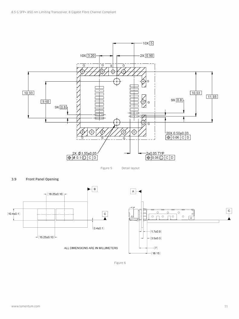
3.9 Front Panel Opening
Figure 6

8.5 G SFP+ 850 nm Limiting Transceiver, 8 Gigabit Fibre Channel Compliant
www.lumentum.com 12
3.10 Module Outline
All dimensions is in millimeters
Figure 7
3.11 Transceiver Belly-to-belly Mounting
Figure 8

8.5 G SFP+ 850 nm Limiting Transceiver, 8 Gigabit Fibre Channel Compliant
www.lumentum.com 13
Section 4 Related Information
Other information related to the SFP+ optical transceiver includes:
Section 4.1 Digital diagnostic monitoring and serial ID operation
Section 4.2 Package and handling instructions
Section 4.3 ESD discharge (ESD)
Section 4.4 Eye safety
4.1 Digital Diagnostic Monitoring and Serial ID OperationThe PLRXPL-Vx-SH4-23-N optical transceiver is equipped with a two-wire serial EEPROM that is used to store specific information about the type and identification of the transceiver as well as real-time digitized information relating to the transceiver’s performance. See the Small Form Factor Committee document number SFF-8472 Revision 10.3, dated December 1, 2007 for memory/address organization of the identification data and digital diagnostic data. The enhanced digital diagnostics feature monitors five key transceiver parameters which are internally calibrated and should be read as absolute values and interpreted as follows:
Transceiver Temperature in degrees Celsius: Internally measured. Represented as a 16 bit signed two’s complement value in increments of 1/256°C from -40 to +85°C with LSB equal to 1/256°C. Accuracy is ± 3°C over the specified operating temperature and voltage range.
Vcc/Supply Voltage in Volts: Internally measured. Represented as a 16-bit unsigned integer with the voltage defined as the full 16-bit value(0 – 65535) with LSB equal to 100 uV with a measurement range of 0 to +6.55 V. Accuracy is ± three percent of nominal value over the specified operating temperature and voltage ranges.
TX Bias Current in mA: Represented as a 16-bit unsigned integer with current defined as the full 16-bit value (0 – 65535) with LSB equal to 2 uA with a measurement range of 0 – 131 mA. Accuracy is ± 10 percent of nominal value over the specified operating temperature and voltage ranges.
TX Output Power in mW: Represented as a 16-bit unsigned integer with the power defined as the full 16-bit value (0 – 65535) with LSB equal to 0.1 uW. Accuracy is ± 2 dB over the specified temperature and voltage ranges over the range of -10 dBm to 0 dBm. Data is not valid when transmitter is disabled.
RX Received Optical Power in mW: Represented as average power as a 16-bit unsigned integer with the power defined as the full 16-bit value (0 – 65535) with LSB equal to 0.1 uW. Accuracy is ± 3 dB over the specified temperature and voltage ranges over the power range of -14 dBm to 0 dBm.
Reading the dataThe information is accessed through the SCL and SDA connector pins of the module. The SFF-8431 Revision 3.2 specification contains all the timing and addressing information required for accessing the data in the EEPROM.
The device address used to read the Serial ID data is 1010000X(A0h), and the address to read the diagnostic data is 1010001X(A2h). Any other device addresses will be ignored.
MOD_ABS, pin 6 on the transceiver, is connected to Logic 0 (Ground) on the transceiver.
SCL, pin 5 on the transceiver, is connected to the SCL pin of the EEPROM.
SDA, pin 4 on the transceiver, is connected to the SDA pin of the EEPROM.
The EEPROM Write Protect pin is internally tied to ground with no external access, allowing write access to the customer-writable field (bytes 128 – 247 of address 1010001X).
Note: address bytes 0 – 127 are not write protected and may cause diagnostic malfunctions if written over.
Decoding the dataThe information stored in the EEPROM, including the organization and the digital diagnostic information, is defined in the Small Form Factor Committee document SFF-8472 Revision 10.3, dated December 1, 2007.
Data Field Descriptions
0
95
127
255
0
95
127
255
55
119
247
Serial ID Information;
Dened by SFP MSA
Reserved for SFP MSA
Alarm and Warning Limits
Reserved for External
Calibration Constants
Real Time Diagnostic
Information
Non volatile, customer-
writeable, eld-writeable area
Address(1010000X)(A0h) Address(1010001X)(A2h)
Lumentum-Specic Information
Lumentum-Specic Information
Lumentum-Specic Information
8.5 G SFP+ 850 nm Limiting Transceiver, 8 Gigabit Fibre Channel Compliant
www.lumentum.com 14
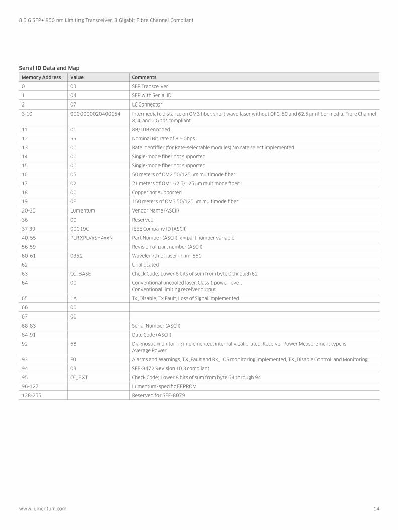
Serial ID Data and Map
Memory Address Value Comments
0 03 SFP Transceiver
1 04 SFP with Serial ID
2 07 LC Connector
3-10 0000000020400C54 Intermediate distance on OM3 fiber, short wave laser without OFC, 50 and 62.5 µm fiber media, Fibre Channel 8, 4, and 2 Gbps compliant
11 01 8B/10B encoded
12 55 Nominal Bit rate of 8.5 Gbps
13 00 Rate Identifier (for Rate-selectable modules) No rate select implemented
14 00 Single-mode fiber not supported
15 00 Single-mode fiber not supported
16 05 50 meters of OM2 50/125 µm multimode fiber
17 02 21 meters of OM1 62.5/125 µm multimode fiber
18 00 Copper not supported
19 0F 150 meters of OM3 50/125 µm multimode fiber
20-35 Lumentum Vendor Name (ASCII)
36 00 Reserved
37-39 00019C IEEE Company ID (ASCII)
40-55 PLRXPLVxSH4xxN Part Number (ASCII), x = part number variable
56-59 Revision of part number (ASCII)
60-61 0352 Wavelength of laser in nm; 850
62 Unallocated
63 CC_BASE Check Code; Lower 8 bits of sum from byte 0 through 62
64 00 Conventional uncooled laser, Class 1 power level, Conventional limiting receiver output
65 1A Tx_Disable, Tx Fault, Loss of Signal implemented
66 00
67 00
68-83 Serial Number (ASCII)
84-91 Date Code (ASCII)
92 68 Diagnostic monitoring implemented, internally calibrated, Receiver Power Measurement type is Average Power
93 F0 Alarms and Warnings, TX_Fault and Rx_LOS monitoring implemented, TX_Disable Control, and Monitoring.
94 03 SFF-8472 Revision 10.3 compliant
95 CC_EXT Check Code; Lower 8 bits of sum from byte 64 through 94
96-127 Lumentum-specific EEPROM
128-255 Reserved for SFF-8079

8.5 G SFP+ 850 nm Limiting Transceiver, 8 Gigabit Fibre Channel Compliant
www.lumentum.com 15
Diagnostics Data Map
Memory Address Value Comments
00-01 Temp High Alarm MSB at low address
02-03 Temp Low Alarm MSB at low address
04-05 Temp High Warning MSB at low address
06-07 Temp Low Warning MSB at low address
08-09 Voltage High Alarm MSB at low address
10-11 Voltage Low Alarm MSB at low address
12-13 Voltage High Warning MSB at low address
14-15 Voltage Low Warning MSB at low address
16-17 Bias High Alarm MSB at low address
18-19 Bias Low Alarm MSB at low address
20-21 Bias High Warning MSB at low address
22-23 Bias Low Warning MSB at low address
24-25 TX Power High Alarm MSB at low address
26-27 TX Power Low Alarm MSB at low address
28-29 TX Power High Warning MSB at low address
30-31 TX Power Low Warning MSB at low address
32-33 RX Power High Alarm MSB at low address
34-35 RX Power Low Alarm MSB at low address
36-37 RX Power High Warning MSB at low address
38-39 RX Power Low Warning MSB at low address
40-55 Reserved For future monitoring quantities
56-59 RP4 External Calibration Constant
60-63 RP3 External Calibration Constant
64-67 RP2 External Calibration Constant
68-71 RP1 External Calibration Constant
72-75 RP0 External Calibration Constant
76-77 Islope External Calibration Constant
78-79 Ioffset External Calibration Constant
80-81 TPslope External Calibration Constant
82-83 TPoffset External Calibration Constant
84-85 Tslope External Calibration Constant
86-87 Toffset External Calibration Constant
88-89 Vslope External Calibration Constant
90-91 Voffset External Calibration Constant
92-94 Reserved Reserved
95 Checksum Low order 8 bits of sum from 0 – 94
96 Temperature MSB Internal temperature AD values
97 Temperature LSB
98 Vcc MSB Internally measured supply voltage AD values
99 Vcc LSB
100 TX Bias MSB (Note 1) TX Bias Current AD values

8.5 G SFP+ 850 nm Limiting Transceiver, 8 Gigabit Fibre Channel Compliant
www.lumentum.com 16
Diagnostics Data Map (Continued)
Memory Address Value Comments
101 TX Bias LSB (Note 1)
102 TX Power MSB (Note 1) Measured TX output power AD values
103 TX Power LSB (Note 1)
104 RX Power MSB Measured RX input power AD values
105 RX Power LSB
106 Reserved MSB For 1st future definition of digitized analog input
107 Reserved LSB
108 Reserved MSB For 2nd future definition of digitized analog input
109 Reserved LSB
110-7 Tx Disable State Digital State of Tx Disable Pin
110-6 Soft Tx Disable Control Writing “1” OR pulling the Tx_Disable pin will disable the laser
110-5 Reserved
110-4 Rate Select State Digital State of Rate Select Pin
110-3 Soft Rate Select Control Writing to this bit has no effect
110-2 Tx Fault State Digital State
110-1 LOS State Digital State
110-0 Data Ready State Digital State; “1” until transceiver is ready
111 Reserved Reserved
112-119 Optional alarm & warning flag bits (Note 2) Refer to SFF-8472 Revision 10.3
120-127 Vendor specific Lumentum specific
128-247 User/Customer EEPROM Field writeable EEPROM
248-255 Vendor specific Vendor-specific control
Note:
1. During Tx disable, Tx bias and Tx power will not be monitored.
2. Alarm and warning are latched. The flag registers are cleared when the system Reads AND the alarm/warning condition no longer exists.

8.5 G SFP+ 850 nm Limiting Transceiver, 8 Gigabit Fibre Channel Compliant
www.lumentum.com 17
4.2 Package and Handling InstructionsThis product is not compatible with any aqueous wash process.
Process plugThe PLRXPL-Vx-SH4-23-N optical transceiver is supplied with a process plug. This plug protects the transceiver optics during standard manufacturing processes by preventing contamination from air borne particles.
Note: It is recommended that the dust cover remain in the transceiver whenever an optical fiber connector is not inserted.
Recommended cleaning and degreasing chemicalsLumentum recommends the use of methyl, isopropyl and isobutyl alcohols for cleaning.
Do not use halogenated hydrocarbons (trichloroethane, ketones such as acetone, chloroform, ethyl acetate, MEK, methylene chloride, methylene dichloride, phenol, N-methylpyrolldone).
FlammabilityThe housing is made of cast zinc and sheet metal.
4.3 Electrostatic Discharge (ESD)
HandlingNormal ESD precautions are required during the handling of this module. This transceiver is shipped in ESD protective packaging. It should be removed from the packaging and handled only in an ESD protected environment utilizing standard grounded benches, floor mats, and wrist straps.
Test and operationIn most applications, the optical connector will protrude through the system chassis and be subjected to the same ESD environment as the system. Once properly installed in the system, this transceiver should meet and exceed common ESD testing practices and fulfill system ESD requirements.
Typical of optical transceivers, this module’s receiver contains a highly sensitive optical detector and amplifier which may become temporarily saturated during an ESD strike. This could result in a short burst of bit errors. Such an event may require the application to reacquire synchronization at the higher layers (serializer/deserializer chip).
4.4 Eye Safety
The PLRXPL-Vx-SH4-23-N Optical Transceiver is a CLASS 1 LASER PRODUCT as defined by the international standard IEC 60825-1:1993+A1:1997+A2:2001 and by U.S.A. regulations for Class 1 products per CDRH 21 CFR 1040.10 and 1040.11. Laser emissions from Class 1 laser products are not considered hazardous when operated according to product specifications. Operating the product with a power supply voltage exceeding 4.0 volts may compromise the reliability of the product, and could result in laser emissions exceeding Class 1 limits.
CautionTampering with this laser based product or operating this product outside the limits of this specification may be considered an act of “manufacturing,” and will require, under law, recertification of the modified product with the U.S. Food and Drug Administration (21 CFR 1040).
The use of optical instruments with this product will increase eye hazard.

North AmericaToll Free: 844 810 LITE (5483)
Outside North AmericaToll Free: 800 000 LITE (5483)
ChinaToll Free: 400 120 LITE (5483)
© 2015 Lumentum Operations LLCProduct specifications and descriptions in this document are subject to change without notice.
plrxpl-vx-sh4-23-n-ds-oc-ae 30162600 902 1110www.lumentum.com
Ordering InformationFor more information on this or other products and their availability, please contact your local Lumentum account manager or Lumentum directly at [email protected].
Part Number Product Description
PLRXPL-VC-SH4-23-N 8 G SFP+ SW, limiting electrical interface, 0 – 70˚C, ± 10% Vcc, no rate select, generic
PLRXPL-VE-SH4-23-N 8 G SFP+ SW, limiting electrical interface, -5 – 85˚C, ± 10% Vcc, no rate select, generic


![INDEX [assets.cambridge.org]assets.cambridge.org/97811070/21792/index/9781107021792...INDEX 745 VCCR (Vienna Convention on Consular Relations (1963)) VCCR (OP) (Vienna Convention on](https://img.pdfslide.us/doc/110x75/5f0b9c2c7e708231d4315a66/index-index-745-vccr-vienna-convention-on-consular-relations-1963-vccr.jpg)