Embed Size (px)
Citation preview

840 IEEE TRANSACTIONS ON POWER ELECTRONICS, VOL. 30, NO. 2, FEBRUARY 2015
Analysis of Dual-Carrier Modulator for BidirectionalNoninverting Buck–Boost Converter
Ilan Aharon, Student Member, IEEE, Alon Kuperman, Member, IEEE, and Doron Shmilovitz, Senior Member, IEEE
Abstract—A pulse-width modulation modulator for a noninvert-ing bidirectional buck–boost converter is analyzed and a corre-sponding average-mode current controller design is revealed. Themain feature of the modulator is the ability to create switching se-quences for both converter legs without requiring any informationregarding either operation mode or the direction of power flow.The modulator receives a control signal generated by the currentcontroller, and a triangular carrier and generates driving signalswith two different duty cycles, allowing tight control of the induc-tor current throughout the entire operating range. The underlyingcircuitry is thus relatively simple; moreover, the proposed methodgreatly simplifies the outer loop controller design. The revealedfindings are supported by simulations and experiments.
Index Terms—Average mode control, bidirectional buck–boostconverter, pulse-width modulation (PWM) modulator.
I. INTRODUCTION
THE ever-increasing energy demands, accompanied by theneed for flexible generation, transmission and distribution,
environmental impact concerns and the need for energy savings,have elevated the development of microgrids, integrating dis-tributed resources into a smarter grid [1]–[5]. Nevertheless, dueto the increasing penetration of intermittent (renewable or al-ternative) energy sources into microgrids, substantial amountsof energy storage are required to maintain the instantaneousbalance between generation and consumption [6] because inter-mittent sources may be perceived as part of the system load [7].
To allow for generation-consumption matching, the energystorage operation is bidirectional, absorbing excessive energywhen generation exceeds the demand and releasing energy whenthe demand exceeds generation [6]. For a typical dc microgridsection, shown in Fig. 1, an energy storage unit may be coupledto the dc bus or either directly or via a bidirectional power elec-tronics interface. Initially, batteries were the most frequently
Manuscript received December 12, 2013; revised February 23, 2014; acceptedMarch 24, 2014. Date of publication April 7, 2014; date of current version Oc-tober 7, 2014. Recommended for publication by Associate Editor D. Vinnikov.
I. Aharon is with the Department of Physical Electronics, School of Electri-cal Engineering, Tel Aviv University, Tel Aviv 69978, Israel, and also with theHybrid Energy Sources Laboratory, Department of Electrical Engineering andElectronics, Ariel University, Ariel 40700, Israel (e-mail: [email protected]).
A. Kuperman is with the Hybrid Energy Sources Laboratory, Departmentof Electrical Engineering and Electronics, Ariel University, Ariel 40700, Israel(e-mail: [email protected]).
D. Shmilovitz is with the Department of Physical Electronics, School ofElectrical Engineering, Tel Aviv University, Tel Aviv 69978, Israel (e-mail:[email protected]).
Color versions of one or more of the figures in this paper are available onlineat http://ieeexplore.ieee.org.
Digital Object Identifier 10.1109/TPEL.2014.2315993
Fig. 1. Typical dc microgrid section.
Fig. 2. BDNIBB converter.
used electrical energy storage units; however, recent develop-ments in the field of supercapacitors have made supercapacitorsa viable alternative to other energy storage technologies [8]. Toeffectively utilize a supercapacitor, it is usually decoupled fromthe dc bus by a power converter. In such a case, the superca-pacitor’s voltage may be controlled independently according tothe desired amount of energy taken from/supplied to the device.Evidently, larger supercapacitor voltage swing allows either al-leviating energy exchange or selecting a smaller supercapacitor.Hence, using a bidirectional buck–boost converter as the powerinterface completely decouples the supercapacitor from dc busvoltages.
Bidirectional converters are generally divided into isolated[9], [10] and nonisolated [11], [12] types. In the case wheregalvanic isolation is not required, a noninverting buck–boostconverter is probably the most versatile topology, supportingBUCK, BOOST, and BUCK–BOOST operations [13]–[17].The synchronous version of the converter (cf. Fig. 2) allowsbidirectional power flow. When a bidirectional noninvertingbuck–boost (BDNIBB) converter is voltage mode controlled
0885-8993 © 2014 IEEE. Personal use is permitted, but republication/redistribution requires IEEE permission.See http://www.ieee.org/publications standards/publications/rights/index.html for more information.

AHARON et al.: ANALYSIS OF DUAL-CARRIER MODULATOR FOR BIDIRECTIONAL NONINVERTING BUCK–BOOST CONVERTER 841
(utilizing either hard or soft switching [18]), the controller andmodulator must be carefully designed to treat inherent nonlin-earities and nonsmooth transients of mode transitions, whichoccur if the BUCK–BOOST operation is skipped to improveefficiency [19]–[23]. Dual-loop control structures for unidirec-tional versions of the BDNIBB converter were proposed in [23]and [24].
However, designing a peak-current mode controller for a bidi-rectional multimode converter is not a simple task because themodulator requires information regarding both operation modeand power flow direction [26], burdening the control circuitry.In general, converter legs must be operated with different dutycycles to avoid nonsmoothness of voltage transfer function gainsat mode transitions. In the case of average-current mode con-trol, the current loop compensator outputs a single modulatingsignal to the modulator, which generates switching commandsto both legs according to the operation mode and power flowdirection. A modulator performing the aforementioned task wasintroduced in [22], and applied to a unidirectional BDNIBBconverter. The main feature of this modulator was its abilityto generate switching sequences without needing informationregarding either the operation mode or the direction of powerflow.
In this paper, the modulator presented in [22] is general-ized and extended to the average current-controlled bidirectionalBDNIBB converter. Comprehensive analysis of the modulatoroperation is carried out and current controller based on the pro-posed modulator is designed. It is shown that when the proposedmodulator is adopted, the control-to-output transfer-functiongain of the current loop remains unchanged upon mode tran-sitions and the corresponding plants differ only in terms ofdisturbance.
The rest of the paper is arranged as follows. Section II revealsoperation modes and control configuration of the BDNIBB con-verter. The modulator structure is discussed and analyzed inSection III, followed by the design of the inner loop controller,discussed in Section IV. The proposed system is verified bymeans of simulations and experiments in Section V, and thepaper is concluded in Section VI.
II. CONVERTER OPERATION MODES
AND CONTROL STRUCTURE
Fig. 2 shows that the BDNIBB power stage is formed bycascading two synchronous converter legs, sharing a commoninductor L. The capacitors C1 and C2 are high-frequency bypasscapacitors, intended to suppress current ripple at the converterterminals. Both legs are driven by different pulse-width mod-ulation (PWM) signals while two switches of the same leg areoperated in complementary fashion, i.e., Qi receives the invertedversion of the signal driving Qi (i = 1, 2). Note that Q1 is theupper switch of leg 1 while Q2 is the lower switch of leg 2.Thus, legs 1 and 2 are often referred to as BUCK and BOOSTlegs, respectively.
The operation of each leg is derived from the behavior of anappropriate synchronous converter. Consequently, if v1 > v2 ,the switches of leg 1 are driven by a PWM signal while Q2 is
Fig. 3. Typical cascaded control structure of a BDNIBB converter.
Fig. 4. Equivalent modulator realizations.
off and the BDNIBB converter is said to be operating in BUCKmode. If v1 < v2 , then the switches of leg 2 are driven by aPWM signal while Q1 is on and the power stage is said tobe operating in BOOST mode. Finally, if v1≈v2 (the detailedlimits will be discussed later on), then both legs are PWM-drivenand the converter operates in BUCK–BOOST mode. Hence,even though the reference direction of power flow is chosenas v1→v2 , the three-mentioned operating modes are valid forboth directions of power flow (e.g., if the switches of leg 1 aredriven by a PWM signal while Q2 is off, the converter wouldbe operating in BUCK mode for either power flow direction).
The typical cascaded control structure of the BDNIBB con-verter is shown in Fig. 3 [27]. Usually, one of the four terminalvariables is chosen to be stabilized, i.e., y ∈ {v1 , i1 , v2 , i2} andr is the corresponding reference signal. The outer loop con-troller generates current reference signal iREF , which, in thecase of average current control (adopted here), corresponds toinductor current averaged over one switching cycle. The differ-ence between the reference and measured current is processedby an inner loop controller, and a control input d to the PWMmodulator is generated (0 < d < 1 for unidirectional operationand −1 < d < 1 for bidirectional operation) [28]. Althoughthe BDNIBB converter legs are driven by two different PWMsignals, for the modulator analyzed in the paper, a single controlsignal d is sufficient in addition to carrier signal vC for creat-ing both converter legs driving PWM signals Q1 and Q2 withcorresponding duty cycles d1 and d2 . Moreover, the modulatorrequires information regarding neither the direction of the powerflow nor the operating mode. The description of the modulatorand comprehensive analysis follows.
III. MODULATOR STRUCTURE AND ANALYSIS
The presented modulator can be realized using one of the twoequivalent structures, shown in Fig. 4 [22]. In the first structure[cf. Fig. 4(a)], the control signal created by the inner loop con-troller is split into two shifted and scaled control signals, whichare compared to the same carrier wave to create correspondingPWM driving signals. In the second structure [cf. Fig. 4(b)],the control signal created by the current controller is comparedto two shifted and scaled carrier waves to create corresponding

842 IEEE TRANSACTIONS ON POWER ELECTRONICS, VOL. 30, NO. 2, FEBRUARY 2015
Fig. 5. Modulator signals.
PWM driving signals (note that in reality carrier waves vC 1 andvC 2 should not be actually produced by scaling high-frequencycarrier wave vC but created independently). The second struc-ture is discussed here and implemented in the further presentedprototype; nevertheless, the findings are valid for the first struc-ture as well.
Consider the modulator structure shown in Fig. 4(b), where−1 < d < 1 is the control input to the PWM modulator createdby the inner loop controller (cf. Fig. 3) and the carrier wave vC
is defined by
vC (t) =
{−1 + 4
TSt, 0 ≤ t ≤ TS
2
3 − 4TS
t, TS
2 ≤ t ≤ TS .(1a)
Shifted and scaled triangular carrier waves for structure twoare given by
vC 1(t) =
{−1 + 2
TS(1 + VH )t, 0 ≤ t ≤ TS
2
2VH + 1 − 2TS
(1 + VH )t, TS
2 ≤ t ≤ TS
vC 2(t) =
{VL + 2
TS(1 − VL )t, 0 ≤ t ≤ TS
2
2 − VL − 2TS
(1 − VL )t, TS
2 ≤ t ≤ TS
(1b)
with Ts being the switching period, as shown in Fig. 5. DrivingPWM signals of legs 1 and 2 are created by comparing d withvC 1 and vC 2 , respectively. In general, offsets VH and VL maybe either positive, negative, or zero. Moreover, |VH | may bedifferent from |VL |. If VL > VH , a nonswitching region, will becreated for VH < d < VL , i.e., Q1 and Q2 will conduct perma-nently, then directly connecting v1 to v2 in steady state, whichmay be useful if a soft source (e.g., solar panel) is connectedto one of the converter’s terminals [29]. Nevertheless, only thecase where VL < VH will be further discussed.
From Fig. 5, the duty cycles of legs 1 and 2 are given by
d1 =
⎧⎪⎨⎪⎩
0, d ≤ −1
KH (1 + d), −1 ≤ d ≤ VH
1, d ≥ VH
d2 =
⎧⎪⎨⎪⎩
0, d ≤ VL
KL (d − VL ), VL ≤ d ≤ 1
1, d ≥ 1
(2)
respectively, with KH = (1 + VH )−1 and KL = (1 – VL )−1 , andare plotted versus d in Fig. 6. While the control signal d residesbetween –1 and 1, the duty cycles are bounded by 0 and 1.
Fig. 6. Duty cycles of converter legs as functions of control signal d.
Fig. 7. BDNIBB converter operating regions and transition boundaries values.
Fig. 8. Overall static voltage transfer function.
Consequently, the operating modes of the converter, as wellas the control signal and duty cycle values at transition bound-aries, are summarized in Fig. 7. The BDNIBB converter willoperate in BUCK mode for −1 < d < VL , BOOST mode forVH < d < 1 and BUCK–BOOST mode for VL < d < VH . Notethat the operation in BUCK–BOOST region should be avoidedif the design is efficiency oriented [22], [23]. However, allowinga small BUCK–BOOST region provides a smooth mode transi-tion between operating modes and a high di/dt, enhancing thedynamic response of the current loop.
Applying the inductor volt–second balance law in each oper-ation mode, the following static voltage transfer functions maybe derived:
M(D) =V2
V1=
⎧⎪⎪⎪⎪⎪⎨⎪⎪⎪⎪⎪⎩
KH (1 + D) , BUCK
KH (1 + D)KL (1 − D)
, BUCK-BOOST
1KL (1 − D)
, BOOST
(3)
where D,V2 and V1 are the steady-state dc components of d, v2and v1 , respectively. The overall static voltage transfer functionis shown in Fig. 8 and is apparently continuous.
It is interesting to note that for D = 0, the static voltage trans-fer function is M(D) = KH K−1
L and will be unity for KH =

AHARON et al.: ANALYSIS OF DUAL-CARRIER MODULATOR FOR BIDIRECTIONAL NONINVERTING BUCK–BOOST CONVERTER 843
Fig. 9. Average model of a BDNIBB converter.
Fig. 10. Closed inner loop of a BDNIBB converter.
TABLE IRELEVANT SIMULATION DATA
KL (or VH = −VL ). In general, the static voltage transfer func-tion attains unity for D = (KL − KH )(KL+KH )−1 .Therefore,symmetry in duty cycle domain leads to asymmetry in the volt-age domain and vice versa: if VH = −VL is selected, the con-verter will operate in BUCK–BOOST mode for the range ofvoltages, satisfying M1≤M(D) ≤ M2 (cf. Fig. 8) with M1 =(1 – VH )(1 + VH )−1 and M2 = (1 + VH )(1 – VH )−1 . Thisrange is asymmetric with respect to M(D) = 1 because 1 −M1 �=M2 – 1. If a symmetric BUCK–BOOST band is required,the following must hold:
1 − VL
1 − VH− 1 = 1 − 1 + VL
1 + VH(4)
which is valid for VH = 0. To verify this finding, consider asingle cell lithium-ion battery feeding a 3.3 V microproces-sor via a BDNIBB converter. The battery voltage varies from4.2 V (fully charged) down to 2.5 V (fully depleted). SelectingVH = −VL = 0.1 defines the BUCK–BOOST region of opera-tion for battery voltages residing between 4.03 and 2.7 V, whichis obviously asymmetric around the voltage of 3.3 V. In contrast,selecting VH = 0 and VL = −0.2 leads to a BUCK–BOOSTregion of operation for battery voltages in the range of 3.96 –2.64 V, which is symmetric with respect to the load voltage.
Another important particular case is VH = VL = 0. Here,the BUCK–BOOST mode of operation is eliminated. The dutycycles of the legs are then given by
d1 =
⎧⎪⎨⎪⎩
0, d ≤ −1
1 + d, −1 ≤ d ≤ 0
1, d ≥ 0
d2 =
⎧⎪⎨⎪⎩
0, d ≤ 0
d, 0 ≤ d ≤ 1
1, d ≥ 1(5)
Fig. 11. Full-scale and zoomed simulation results. (a) Upper: reference andinductor currents; middle: terminal voltages; bottom: PWM driving signals(signal to Q2 shifted up by 1). (b) Upper: zoomed terminal voltages; bottom:zoomed PWM driving signals.
and the static voltage transfer functions (3) consequently reduceto
M(D) =
⎧⎪⎨⎪⎩
1 + D, BUCK
11 − D
, BOOST.(6)
Therefore, at transition boundary (D = 0), MBUCK =MBOOST = 1 and the transition is smooth in terms of staticgain (cf. Fig. 8). However, in such a case, a real BDNIBBconverter may suffer from the presence of an operational “deadzone” which exists near BUCK to BOOST (and back) transition,arising from unavoidable nonidealities, potentially giving riseto drawbacks such as poor regulation and instability [25], [26].
IV. INNER LOOP CONTROLLER DESIGN
To utilize the presented modulator with the control structureshown in Fig. 3, the inner loop controller should be designedfirst. Next, it is shown that the current loop of the BDNIBBconverter may be represented by a single plant structure for all

844 IEEE TRANSACTIONS ON POWER ELECTRONICS, VOL. 30, NO. 2, FEBRUARY 2015
Fig. 12. Simulation results. Upper: terminal voltages; middle: carrier wavesand control signal; bottom: PWM driving signals. (a) Buck mode. (b) Buck–boost mode. (c) Boost mode.
three operating modes. Hence, a single current controller maybe designed.
The average model of the BDNIBB converter (valid for bothpower flow directions) is shown in Fig. 9 [30]. In general,
Fig. 13. Picture of the BDNIBB converter-based battery-supercapacitor hy-brid prototype.
inductor current dynamics are nonlinear, dictated by
LdiLdt
= d1v1 − (1 − d2)v2 . (7)
Combining (2) with (7), the inductor dynamics in each of theoperation modes may be expressed as a function of the controlinput d as
LdiL
dt=
⎧⎪⎪⎨⎪⎪⎩
KH (1 + d) v1 − v2 , BUCK
KH (1 + d) v1 − KL (1 − d) v2 , BUCK − BOOST
v1 − KL (1 − d) v2 , BOOST.(8)
Splitting the time-based variables into dc and ac components
d = D + d, iL = IL + iL , v1 = V1 + v1 , v2 = V2 + v2 (9)
and substituting into (8) reveals the small-signal inductor currentdynamics
LdiLdt
=
⎧⎪⎪⎪⎪⎪⎪⎪⎨⎪⎪⎪⎪⎪⎪⎪⎩
KH V1 d + KH (1 + D) v1 − v2 ,
BUCK(KH V1 + KL V2 ) d + KH (1 + D) v1 − KL (1 − D) v2 ,
BUCK − BOOST
KL V2 d + v1 − KL (1 − D) v2 ,
BOOST(10)
around dc operation points, defined by (3). The Laplace trans-form of (10) is taken, and the results are rearranged as follows:
iL (s) =1Ls
(Gd(s) + f(s)
)(11)
with
G =
⎧⎪⎨⎪⎩
KH V1 , BUCK
KH V1 + KLV2 , BUCK − BOOST
KLV2 , BOOST
(12)
and
f =
⎧⎪⎨⎪⎩
KH (1 + D) v1 − v2 , BUCK
KH (1 + D) v1 − KL (1 − D) v2 , BUCK − BOOST
v1 − KL (1 − D) v2 , BOOST(13)

AHARON et al.: ANALYSIS OF DUAL-CARRIER MODULATOR FOR BIDIRECTIONAL NONINVERTING BUCK–BOOST CONVERTER 845
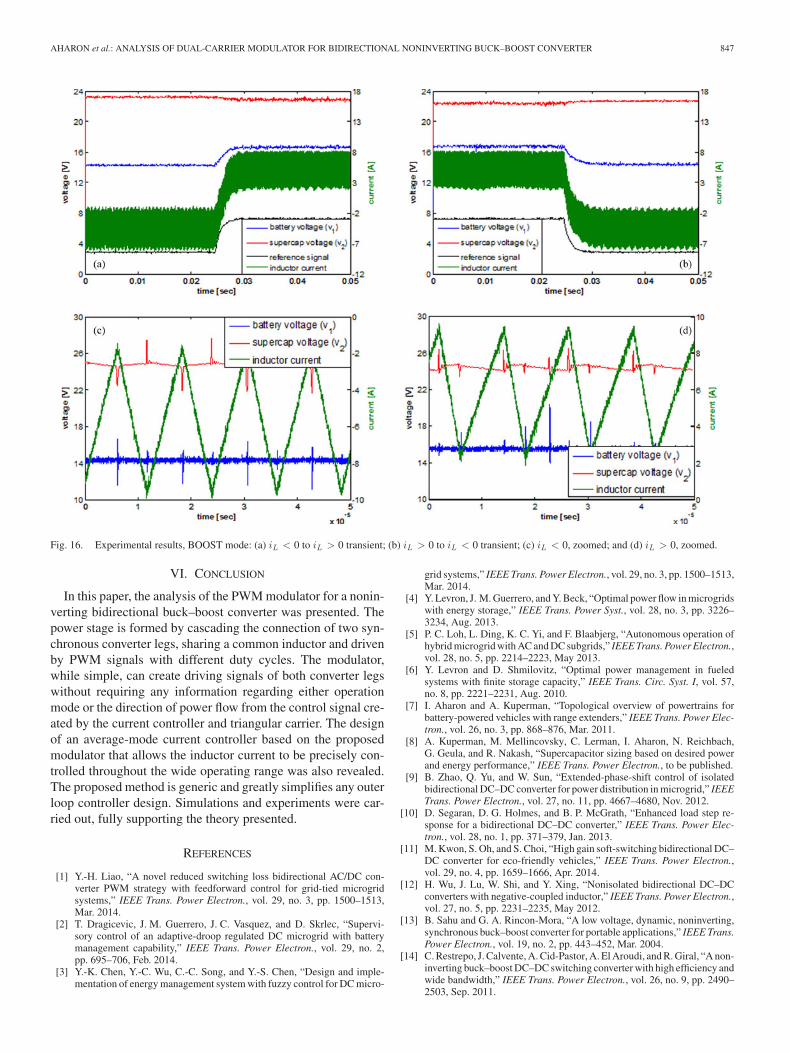
Fig. 14. Experimental results, BUCK mode: (a) iL < 0 to iL > 0 transient; (b) iL > 0 to iL < 0 transient; (c) iL < 0, zoomed; and (d) iL > 0, zoomed.
being the control gain and disturbance, respectively. Further-more, defining
GN =13
(GBUCK + GBUCK−BOOST + GBOOST)
=23
(KH V1 + KLV2) (14)
and rearranging (11) as
iL (s) =1Ls
(GN d(s) + f ′(s)
)(15)
with
f ′(s) = f(s) + (G − GN )d(s), (16)
the current loop in three operation modes may be perceivedto be different in disturbance terms only, possessing a similarcontrol-to-output transfer function
iL
d(s)
∣∣∣∣f ′(s)=0
=GN
Ls. (17)
Hence, from the control point of view, the transition betweenmodes is equivalent to a step change in disturbance and shouldbe properly rejected by the controller. The consequent small-signal inner control loop is shown in Fig. 10, where C(s) isthe controller, stabilizing (17) while rejecting (16), usually ofPI [31] or type-II [30] structures.
Because of the synchronous nature of both legs, current loopis symmetrical for both power flow directions, i.e., (15) holds forany sign of iL . Hence, once current loop is stabilized, the outerloop (usually much slower than the inner loop in microgrid ap-plications [32]) may be constructed assuming iL ∼= iREF , whereiREF is the outer controller output. For examples of outer loopcontroller design (which is outside the scope this paper), referto [33] and [34].
V. VERIFICATION
To verify the operation of the discussed modulator, an idealBDNIBB converter-based battery-supercapacitor hybrid wassimulated first. A 14.8 V ideal battery was connected to leg1 while a 29 F supercapacitor was connected to leg 2 of theconverter. The circuit parameters are summarized in Table I,implying the following partition to operation modes accordingto Fig. 8:⎧⎪⎨
⎪⎩v2 ≤ 12.1V, BUCK
12.1V ≤ v2 ≤ 18.1V, BUCK − BOOST
v2 ≥ 18.1V, BOOST.
(18)
First, the capacitor was charged from 5 to 25 V by settingthe inductor current reference to 4.4 A. Then, the capacitorwas discharged back into the battery by changing the sign ofinductor current reference. A PI current controller was used

846 IEEE TRANSACTIONS ON POWER ELECTRONICS, VOL. 30, NO. 2, FEBRUARY 2015
Fig. 15. Experimental results, BUCK–BOOST mode: (a) iL < 0 to iL > 0 transient; (b) iL > 0 to iL < 0 transient; (c) iL < 0, zoomed; and (d) iL > 0,zoomed.
in the simulations (refer to [31] for detailed controller designguidelines).
Simulation results are presented in Figs. 11 and12. The systemdemonstrates good tracking and disturbance rejection with near-zero steady-state error in bidirectional operation. The three oper-ation modes are well evident from PWM driving signals shownin Fig. 11, and the whole operation is symmetrical; zoomed re-sults demonstrate smooth mode transitions. The supercapacitorcharging/discharging rate is constant in BUCK mode becauseit is directly connected to the inductor, whereas, in BUCK–BOOST and BOOST modes, it depends on the duty cycle of leg2. Zoomed modulator-related signals are shown in Fig. 12 foreach operating mode.
To experimentally validate the simulated battery-supercapacitor hybrid, a 200 W BDNIBB converter wasbuilt, as shown in Fig. 13. An MR-2791 Li-ion battery (14.8 V,15.6 Ah) was connected to leg 1 of the converter while twoseries-connected Maxwell BMOD0058-E016-B02 supercapac-itors (16.2 V, 58 F each) were coupled to leg 2. The inductorcurrent reference signal was created by low-pass filtering andamplify a digital signal processor PWM output (1-bit D/A).
The scaling was as follows: the reference signal of 5 V corre-sponded to the inductor current reference of 0 A, the referencesignal of 0 V corresponded to the inductor current reference of–10 A and the reference signal of 10 V corresponded to the in-ductor current reference of 10 A. A PI-type analog current loop
stabilizing controller was used. Measurements were carried outwith a 400 MHz Lecroy Wave Runner 44 XI-A oscilloscopeand AP015 Lecroy current probe. Because of the battery limi-tations, the inductor current reference was set to ± 4.4 A (i.e.,the reference signal was set to 2.8 V for −4.4 A and 7.2 V for4.4 A).
Experiments were conducted as follows: at each of the threeoperation modes, current reversal (supercapacitor charging →supercapacitor discharging and vice-versa) was performed todemonstrate both bidirectional operation and reference track-ing. Figs. 14–16 demonstrate experimental results for BUCK,BUCK–BOOST, and BOOST modes of operation, respectively.Zoomed versions of the results for each power flow directionare shown as well. Note that iL > 0 implies power flow from su-percapacitor to battery and iL < 0 implies the opposite. At theinstant of inductor current transient from negative to positive(positive to negative), the battery terminal voltage rises (de-creases) while supercapacitor terminal voltage decreases (rises)due to the reversal of the equivalent series resistance (ESR) volt-age drop sign. The change in battery terminal voltage is higherbecause the battery ESR is approximately five times higherthan supercapacitor ESR. Moreover, there is a nontypical in-ductor current shape during BUCK–BOOST mode caused bythe triangular carrier shape (rather than saw-tooth), resulting innonsynchronized switching of the legs leading to four switchingevents during a switching cycle.
AHARON et al.: ANALYSIS OF DUAL-CARRIER MODULATOR FOR BIDIRECTIONAL NONINVERTING BUCK–BOOST CONVERTER 847
Fig. 16. Experimental results, BOOST mode: (a) iL < 0 to iL > 0 transient; (b) iL > 0 to iL < 0 transient; (c) iL < 0, zoomed; and (d) iL > 0, zoomed.
VI. CONCLUSION
In this paper, the analysis of the PWM modulator for a nonin-verting bidirectional buck–boost converter was presented. Thepower stage is formed by cascading the connection of two syn-chronous converter legs, sharing a common inductor and drivenby PWM signals with different duty cycles. The modulator,while simple, can create driving signals of both converter legswithout requiring any information regarding either operationmode or the direction of power flow from the control signal cre-ated by the current controller and triangular carrier. The designof an average-mode current controller based on the proposedmodulator that allows the inductor current to be precisely con-trolled throughout the wide operating range was also revealed.The proposed method is generic and greatly simplifies any outerloop controller design. Simulations and experiments were car-ried out, fully supporting the theory presented.
REFERENCES
[1] Y.-H. Liao, “A novel reduced switching loss bidirectional AC/DC con-verter PWM strategy with feedforward control for grid-tied microgridsystems,” IEEE Trans. Power Electron., vol. 29, no. 3, pp. 1500–1513,Mar. 2014.
[2] T. Dragicevic, J. M. Guerrero, J. C. Vasquez, and D. Skrlec, “Supervi-sory control of an adaptive-droop regulated DC microgrid with batterymanagement capability,” IEEE Trans. Power Electron., vol. 29, no. 2,pp. 695–706, Feb. 2014.
[3] Y.-K. Chen, Y.-C. Wu, C.-C. Song, and Y.-S. Chen, “Design and imple-mentation of energy management system with fuzzy control for DC micro-
grid systems,” IEEE Trans. Power Electron., vol. 29, no. 3, pp. 1500–1513,Mar. 2014.
[4] Y. Levron, J. M. Guerrero, and Y. Beck, “Optimal power flow in microgridswith energy storage,” IEEE Trans. Power Syst., vol. 28, no. 3, pp. 3226–3234, Aug. 2013.
[5] P. C. Loh, L. Ding, K. C. Yi, and F. Blaabjerg, “Autonomous operation ofhybrid microgrid with AC and DC subgrids,” IEEE Trans. Power Electron.,vol. 28, no. 5, pp. 2214–2223, May 2013.
[6] Y. Levron and D. Shmilovitz, “Optimal power management in fueledsystems with finite storage capacity,” IEEE Trans. Circ. Syst. I, vol. 57,no. 8, pp. 2221–2231, Aug. 2010.
[7] I. Aharon and A. Kuperman, “Topological overview of powertrains forbattery-powered vehicles with range extenders,” IEEE Trans. Power Elec-tron., vol. 26, no. 3, pp. 868–876, Mar. 2011.
[8] A. Kuperman, M. Mellincovsky, C. Lerman, I. Aharon, N. Reichbach,G. Geula, and R. Nakash, “Supercapacitor sizing based on desired powerand energy performance,” IEEE Trans. Power Electron., to be published.
[9] B. Zhao, Q. Yu, and W. Sun, “Extended-phase-shift control of isolatedbidirectional DC–DC converter for power distribution in microgrid,” IEEETrans. Power Electron., vol. 27, no. 11, pp. 4667–4680, Nov. 2012.
[10] D. Segaran, D. G. Holmes, and B. P. McGrath, “Enhanced load step re-sponse for a bidirectional DC–DC converter,” IEEE Trans. Power Elec-tron., vol. 28, no. 1, pp. 371–379, Jan. 2013.
[11] M. Kwon, S. Oh, and S. Choi, “High gain soft-switching bidirectional DC–DC converter for eco-friendly vehicles,” IEEE Trans. Power Electron.,vol. 29, no. 4, pp. 1659–1666, Apr. 2014.
[12] H. Wu, J. Lu, W. Shi, and Y. Xing, “Nonisolated bidirectional DC–DCconverters with negative-coupled inductor,” IEEE Trans. Power Electron.,vol. 27, no. 5, pp. 2231–2235, May 2012.
[13] B. Sahu and G. A. Rincon-Mora, “A low voltage, dynamic, noninverting,synchronous buck–boost converter for portable applications,” IEEE Trans.Power Electron., vol. 19, no. 2, pp. 443–452, Mar. 2004.
[14] C. Restrepo, J. Calvente, A. Cid-Pastor, A. El Aroudi, and R. Giral, “A non-inverting buck–boost DC–DC switching converter with high efficiency andwide bandwidth,” IEEE Trans. Power Electron., vol. 26, no. 9, pp. 2490–2503, Sep. 2011.

848 IEEE TRANSACTIONS ON POWER ELECTRONICS, VOL. 30, NO. 2, FEBRUARY 2015
[15] P.-C. Huang, W.-Q. Wu, H.-H. Ho, and K.-H. Chen, “Hybrid buck–boostfeedforward and reduced average inductor current techniques in fast linetransient and high-efficiency buck–boost converter,” IEEE Trans. PowerElectron., vol. 25, no. 3, pp. 719–730, Mar. 2010.
[16] Y.-H. Lee, S.-C. Huang, S.-W. Wang, W.-C. Wu, P.-C. Huang, H.-H. Ho,Y.-T. Lai, and K.-H. Chen, “Power-tracking embedded buck–boost con-verter with fast dynamic voltage scaling for the soc system,” IEEE Trans.Power Electron., vol. 27, no. 3, pp. 1271–1282, Mar. 2012.
[17] A. Khaligh, J. Cao, and Y.-J. Lee, “A multiple-input DC–DC convertertopology,” IEEE Trans. Power Electron., vol. 24, no. 3, pp. 862–868, Mar.2009.
[18] S. Waffler and J. Kolar, “A novel low-loss modulation strategy for high-power bidirectional buck + boost converters,” IEEE Trans. Power Elec-tron., vol. 24, no. 6, pp. 1589–1689, Jun. 2009.
[19] D. C. Jones and R. W. Erickson, “Buck–boost converter efficiency max-imization via a nonlinear digital control mapping for adaptive effectiveswitching frequency,” IEEE J. Emerging Sel. Top. Power Electron., vol. 1,no. 3, pp. 153–165, Sep. 2013.
[20] D. C. Jones and R. W. Erickson, “A nonlinear state machine for deadzone avoidance and mitigation in a synchronous noninverting buck–boostconverter,” IEEE Trans. Power Electron., vol. 28, no. 1, pp. 467–480, Jan.2013.
[21] D. Shmilovitz and Y. Levron, “Distributed maximum power point trackingin photovoltaic systems—Emerging architectures and control methods,”AUTOMATIKA, vol. 53, no. 2, pp. 142–155, Jun. 2012.
[22] Y.-J. Lee, A. Khaligh, and A. Emadi, “A compensation technique forsmooth transitions in a noninverting buck–boost converter,” IEEE Trans.Power Electron., vol. 24, no. 4, pp. 1002–1016, Apr. 2009.
[23] Y.-J. Lee, A. Khaligh, A. Chakraborty, and A. Emadi, “Digital combina-tion of buck and boost converters to control a positive buck–boost converterand improve the output transients,” IEEE Trans. Power Electron., vol. 24,no. 5, pp. 1267–1279, May 2009.
[24] C.-L. Wei, C.-H. Chen, K.-C. Wu, and I.T. Ko, “Design of an average-current-mode noninverting buck–boost DC–DC converter with reducedswitching and conduction losses,” IEEE Trans. Power Electron., vol. 27,no. 12, pp. 4934–4943, Dec. 2012.
[25] C. Restrepo, J. Calvente, A. Romero, E. Vidal-Idiarte, and R. Giral,“Current-mode control of a coupled inductor buck–boost DC–DC switch-ing converter,” IEEE Trans. Power Electron., vol. 27, no. 5, pp. 2536–2549,May 2009.
[26] C.-G. Yoo, W.-C. Lee, and I. Suh, “Current mode PWM controller fora 42V/14V bidirectional DC/DC converter,” in Proc. IEEE 37th PowerElectron. Spec. Conf., Jun. 2006, pp. 18–22.
[27] Z. Chen, “Double loop control of buck–boost converters for wide rangeof load resistance and reference voltage,” IET Contr. Theory Appl., vol. 6,no. 7, pp. 900–910, 2012.
[28] Z. Chen, J. Hu, and W. Gao, “Closed-loop analysis and control of a non-inverting buck–boost converter,” Int. J. Contr., vol. 83, no. 11, pp. 2294–2307, 2010.
[29] Y. Levron and D. Shmilovitz, “Sliding mode control of photovoltaic mod-ule integrated buck–boost converters,” in Proc. 15th Int. Power Electron.Mot. Contr. Conf., Novi Sad, Serbia, Sep. 2012, pp. 4–6.
[30] A. Kuperman, I. Aharon, S. Malki, and A. Kara, “Design of a semiactivebattery-ultracapacitor hybrid energy source,” IEEE Trans. Power Elec-tron., vol. 28, no. 2, pp. 806–815, Feb. 2013.
[31] I. Aharon, A. Kuperman, and D. Shmilovitz, “Analysis of bi-directionalbuck–boost converter for energy storage applications,” in Proc. IEEE 39thInd. Electron. Soc. Ann. Conf., Vienna, Austria, Nov. 2013, pp. 10–13.
[32] T. Pavlovic, T. Bjasic, and Z. Ban, “Simplified averaged models of DC–DCpower converters suitable for controller design ad microgrid simulation,”IEEE Trans. Power Electron., vol. 28, no. 7, pp. 3266–3275, Jul. 2013.
[33] C. Restrepo, T. Konjedic, J. Calvente, M. Milanovic, and R. Giral, “Fasttransitions between current control loops of the coupled-inductor buck–boost DC–DC converter,” IEEE Trans. Power Electron., vol. 28, no. 8,pp. 3648–3652, Aug. 2013.
[34] A. Kuperman, “UDE-based robust voltage control of DC–DC power con-verters,” in Proc. IEEE 5th Int. Congr. Ultra-Modern Telecomm. Contr.Syst., Almaty, Kazakhstan, Sep. 2013, pp. 10–13.
Authors’ photographs and biographies not available at the time of publication.


![Journal of Power Sources - WordPress.com · developed electrochemical cell [19]. One pattern per hour was col-lected; the interval between two consecutive XRD patterns corre-sponding](https://img.pdfslide.us/doc/110x75/5f81870a2dc76102f7783b26/journal-of-power-sources-developed-electrochemical-cell-19-one-pattern-per.jpg)