Embed Size (px)
Citation preview

1
8284 / 8288 Internal
Architecture

2
ROAD MAP
• Memory Addressing In 8086
• 8284 Clock Generator
• Bus Buffering in 8086
• Bus Latching in 8086

3
MEMORY ADDRESSING IN 8086
In 8086 the memory address space can be viewed as a sequence of
one million bytes in which any byte may contain an 8-bit data element
and any two consecutive bytes may contain a 16-bit data element.
The address space is physically connected to a 16-bit data bus by
dividing the address space into two 8-bit banks of up to 512K bytes
each, as depicted in Fig. below

As observed from Fig. 2.2. one bank is connected to the lower half ofthe 16-bit data bus (D0-D7) and contains even address bytes. i.e.when A0 bit is low, the bank is selected.
The other bank is connected to the upper half of the data bus (D8-D15) and contains odd address bytes. That means when A0 is highand BHE (Bus High Enable) is low, the odd bank is selected.
There are four possible ways to access the data from the memory.
Such four ways are as listed below.
8-bit data from lower (Even) address Bank
8-bit data from higher (Odd) address Bank
16-bit data starting from Even Address, and
16-bit data starting from Odd Address.
4

The 8-bit Data from Lower/Even Address Bank:
In this case to access memory bytes from Even address, information is
transferred over the lower half of the data bus (D70-D7), where A0 is output
LOW and BHE is output HIGH enabling only the even address bank. The fig.
depicts the arrangement for this method as below:
5

8-bit Data from Higher/Odd Address Bank:
Here to access memory byte from an odd address information, is
transferred over the higher half of the data bus (D8-D15). The BHE output
low enables the upper memory bank, and whereas A0 is output high to disable
lower memory bank. The arrangement is as depicted in Fig. below.
6

The 16-bit Data Starting from Even-Address:
Here, 16-bit data from an even address is accessed in a single bus cycle.
The address lines A1-A19 select the appropriate byte within each bank. A0
low and BHE low enables both banks simultaneously. The arrangement is as
shown in fig. below.
7

The 16-bit Data Access starting from Odd Address:
Here a 16-bits word located at an odd address (two consecutive bytes with
the least significant byte at an odd byte address) is accessed using two bus
cycles. For first bus cycle, lower byte will be accessed. The arrangement with
odd address as 0005 is as shown in Fig.
8

Now during second bus cycle, the upper byte (with the even address
0006H as observed in fig. 2.6 (b)) will be accessed. During first bus
cycle, A1-A19 address bus specifies the address and A0 as 1 and BHE
is low.
That means the even memory bank will be disabled and odd
memory bank is enabled and next, during second bus cycle, the address
is incremented.
That means, A0 is zero and BHE is made high, and even memory
bank is enabled and the odd memory bank is disabled, as observed in
Fig.
9

8284A Clock Generator The 8284A is an important ancillary component to the
8086/8088 microprocessor. Without clock generator, itrequired many additional circuits to generate the clock in an8086/8088-based system.
8284A provides following basic functions or signals: clockgeneration, RESET synchronization, READY synchronization,and a TTL level peripheral clock signal which are veryimportant essential signal to microprocessors.
The Fig. ahead depicts the details the details of pin out orfunctional pins of the clock generator 8284A.
10

11
8284 Clock Generator ( Pin Configuration)
12

13

14
15
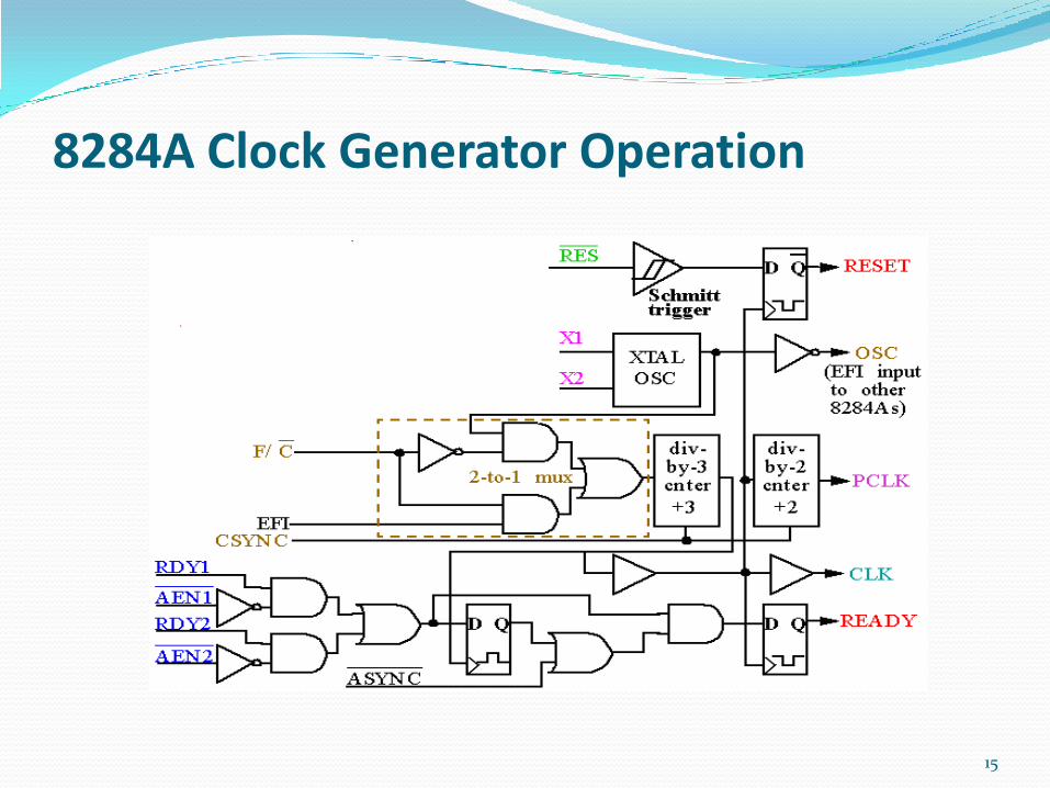
8284A Clock Generator Operation

The two sections of operation those are of interested in 8284A clockgenerator are
Operation of the clock section, and Operation of the Reset section
Operation of the Clock Section:The top half of the logic diagramin Fig. represents the clock and reset synchronization section of the8284A clock generator. As observed, the crystal oscillator has two inputs:XI and X2 when a crystal is attached to XI nd X2, oscillator generates asquare-wave signal at the same frequency as the crystal.
The square-wave so generated signal is fed to an AND gate and also toan inverting buffer that provides the OSC output signal. (The OSC signalis sometimes used as an EFI input to other 8284A circuits in a system).
The inspection of AND gate reveals that when F/C is a logic 0, theoscillator output is steered through to the divide-by-3 counter. If F/C is alogic 1, then EFI is steered through to the counter.
16

The output of the divide-by-3 counter generates timing for
ready synchronization, a signal for another counter (divide-by-2),
and the CLK signal to the 8086/8088 microprocessors.
The CLK signal is also buffered before it leaves the clock
generator. Observe that the output of the first counter feeds the
second.
These two cascaded counters provide the divide-by-6 output at
PCLK, the peripherals clock output, the fig. below; shows the
connection, arrangement of 8284A to 8086/8088 microprocessor.
17

18

From Fig. two points to be observed; i.e.,
That F/C and CSYNC are grounded to select the crystal oscillator and
That a 15 MHz crystal provides the normal 5 MHz clock signal to the8086/8088 as well as a 2.5 MHz peripheral clock signal.
Operation of the Reset Section: The reset section of the 8284A is
simple, and it consists of a Schmitt trigger buffer and a single D-type
flip-flop circuit. The D-type flip-flop ensures that the timing
requirement of the 8086/8088 RESET input are fulfilled.
This circuit applies the RESET signal to the microprocessor on the
negative edge (1-to-0 transition) of each clock. The 8086/8088
microprocessors sample RESET at the positive edge (0-to- 1 transition)
of the clocks; therefore (this circuit meets the timing requirements of the8086/8088).
19

From Fig. it can be observed that an RC circuit provides a logic0 to the RES input pin when power is first applied to the system.
After a short time, the RES input becomes a logic 1 because the
capacitor charges toward +5.0 V through the resistor. A push-
button switch allows the microprocessor to be reset by the
operator.
Exact rest timing requires the RESET input to become a logic 1
no later than four clocks after system power is applied and to be
held for at least 50 µs. (The flip-flop makes certain that RESET
goes high in four clocks, and the RC time constant ensures that itstays high for at least 50 µs).
20

THE BUS BUFFERING AND LATCHING:To make use
of 8086/8088 microprocessor with memory or I/O interfaces,
the multiflexed buses of the µP has to be demultiplexed.
Therefore we have to discuss about demultiplexing the buses,
and mention how buses are buffered in the case of large
system, depending on fan-out of the components. Now let us
discuss about:
Demultiplexing the Buses of 8086/8088, and
Buffered System for 8086/8088.
21

Demultiplexing the Buses of 8086/8088 :
The address/data bus on the 8086/8088 is multiplexed shared so as to reducethe number of pins required for the 8086/8088 integrated circuit. But thisburdens the hardware designer with the task of extracting or demultiplexinginformation from these multiplexed pins. So can we not leave busesmultiplexed.
When the buses are multiplexed, the address changes at the memory and I/O,which causes them to read or write data in the wrong locations.
In all computer systems they have three buses:
(1) An address bus that provides the memory and I/O with the memory addressor the I/O port number,
(2) A data bus that transfers data between the microprocessor and the memoryand I/O in the system, and
(3) A control bus that provides control signals to the memory and I/O. (Thesebuses must be present in order to interface to memory and I/Q).
22

Now let us observe the demultiplexing arrangement for 8086
Demultiplexing the 8086: The 8086 system requires separate
address, data and control buses , which differs primarily in the
number of multiplexed pins. In 8086, the multiplexed pins include
AD15-AD0-A19/S6-A16/S3, and BHE/S7. All of these signals must be
demultiplexed.
The Fig. depicts a demultiplexed 8086 with all three buses: address
(A19-A0 and BHE, data (D15-D0), and control (M/IO, RD and WR), asbelow.
23

24
BUS Buffering and Latching

In the circuit shown in Fig. an additional 74LS373 latch
has been added to demultiplex the address/data bus pins
Ad15-AD8 and a BHE/S7 input has been added to the top
74LS273 to select the high-order memory bank in the
16-bit memory system of the 8086 if compared with that
for 8088.
The memory and I/O system observe the 8086 as a
device with a 20-bit address bus (A19-A0), a 16-bit data
(D15-D0) and a 3 line control bus (M/IO, RD and WR).
25

Demultiplexing the 8086: The Fig. drawn ahead shows
the 8086 microprocessor and the components required to
demultiples its buses. Here, two 74LS373 transparent
latches are used to demultiplex the address/data bus
connections AD7-AD0 and the multiplexed address/status
connections A19/S6-A16/S3 as shown:
26

27

The transparent latches, which are looking like wires whenever the
address latch enable pin (ALE) becomes a logic 1 they pass the
inputs to the outputs.
After a small duration ALE returns to its logic 0 condition, which
causes the latches to remember the inputs at the time of the change
to a logic 0. In this case, A7-A0 are stored in the bottom latch and
A19-A0.
These address connections allow the 8088 to address 1M byte of
memory space. (The fact that the data bus is separate allows it to
be connected to any 8-bit peripheral device or memorycomponent).
28

Buffered System for 8086/8088
When more than 10 unit loads are attached to any bus pin, the entire
8086 or 8088 system must be buffered. The demultiplexed pins are
already buffered by the 74LS373 latches, which have been designed to
drive the high-capacitance buses encountered in microcomputer systems.
A logic 0 output provides up to 32 mA of sink current, and a logic 1
output provides up to 5.2 mA of source current. That means a fully
buffered signal will introduce a timing delay to the system. This causes no
difficulty unless memory or I/O devices are used, which function at near
the maximum speed of the bus.
29

Fully Buffered 8086: The Fig. drawn ahead shows a fully
buffered 8086 microprocessor. It address pins are already
buffered by the 74LS373 address latches; its data bus employs
two 74LS245 octal bi-directional bus buffers; and the control
bus signals, and IO/M, M/IO, RD and WR use a 74LS244buffer.
Fully buffered 8086 system requires one 74LS244, two74LS245s, and three 74LS373s
Note. 8086 requires one more buffer than the 8088 because of
the extra eight data bus connections, D15-D8. It also has a signal
that is buffered for memory-ban selection.
30

31

Wait State:
The Fig. drawn ahead depicts a circuit used to introduce any number of
wait states for 8086/8088 microprocessors, where an 8-bit serial shift register
(74LS164) shifts a logic 0 for one or more clock periods form one if its Q
outputs through to the RDY1 input of the 8284A. With suitable strapping, thiscircuit can provide various number of wait states.
It can also be observed that how, the shift register is cleared back point.
The output of the register is forced high when the second flip-flop captures
RD, WR and INTA pins are all logic I’s. These three signal are high until state
T2, so the shift register shift four the first time when positive edge of the T2
arrives. If one wait is desired, then output QB is connected to the OR gate. Iftwo waits are desired, output Qc is connected, and so forth.
32

Wait State Generator
33

We can observe that this circuit does not always generate
wait states, but is enabled form the memory only for
memory devices that require the insertion of waits.
If the selection signals from a memory device is a logic
0, the device is selected; then this circuit will generate a wait
state.
34

THANKS!
For more Notes Follow http://www.edutechlearners.com