Embed Size (px)
Citation preview
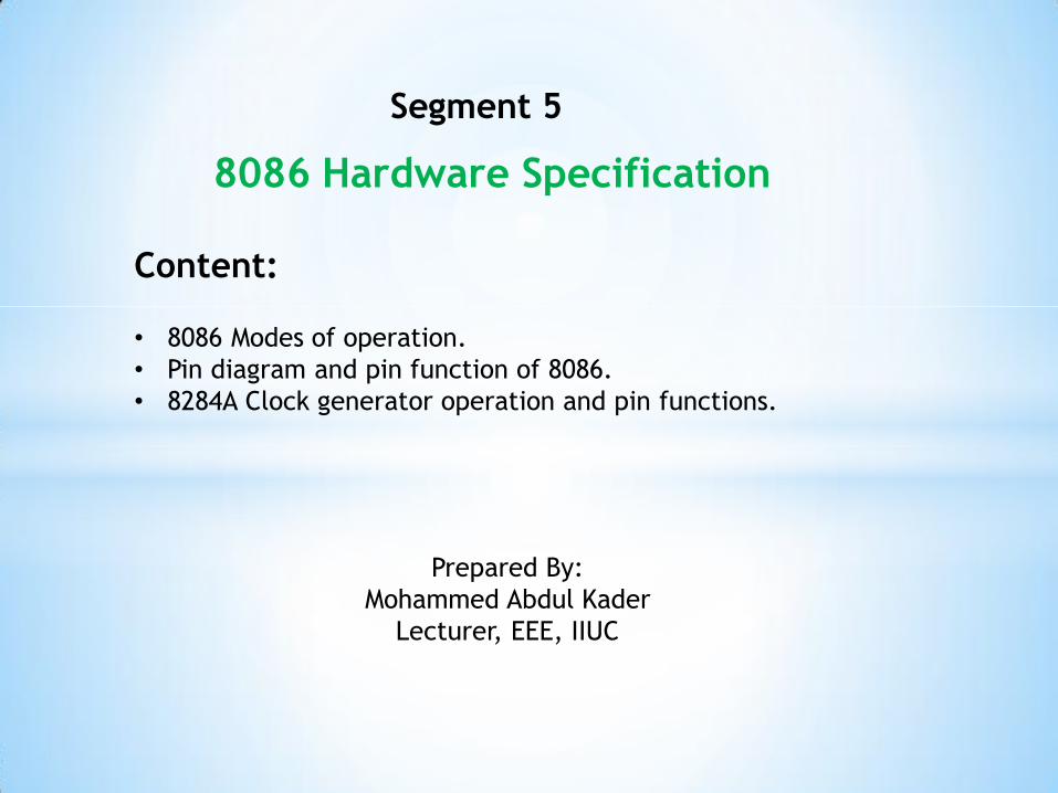
8086 Hardware Specification
Content: • 8086 Modes of operation.
• Pin diagram and pin function of 8086.
• 8284A Clock generator operation and pin functions.
Prepared By:
Mohammed Abdul Kader
Lecturer, EEE, IIUC
Segment 5
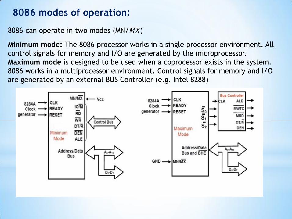
8086 modes of operation:
8086 can operate in two modes (MN/𝑀𝑋)
Minimum mode: The 8086 processor works in a single processor environment. All
control signals for memory and I/O are generated by the microprocessor.
Maximum mode is designed to be used when a coprocessor exists in the system.
8086 works in a multiprocessor environment. Control signals for memory and I/O
are generated by an external BUS Controller (e.g. Intel 8288)
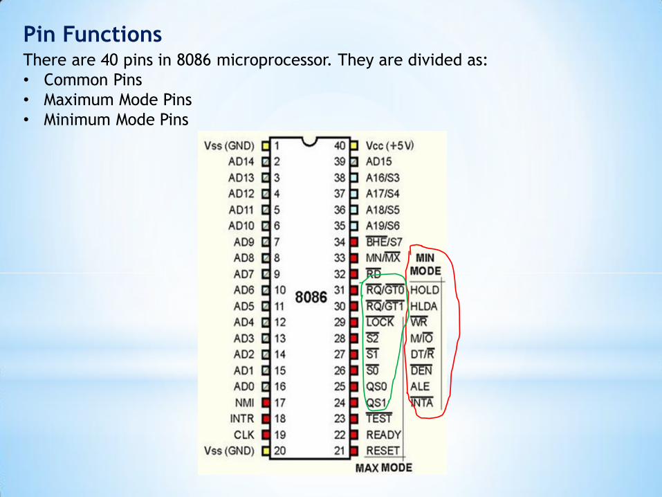
Pin Functions There are 40 pins in 8086 microprocessor. They are divided as:
• Common Pins
• Maximum Mode Pins
• Minimum Mode Pins
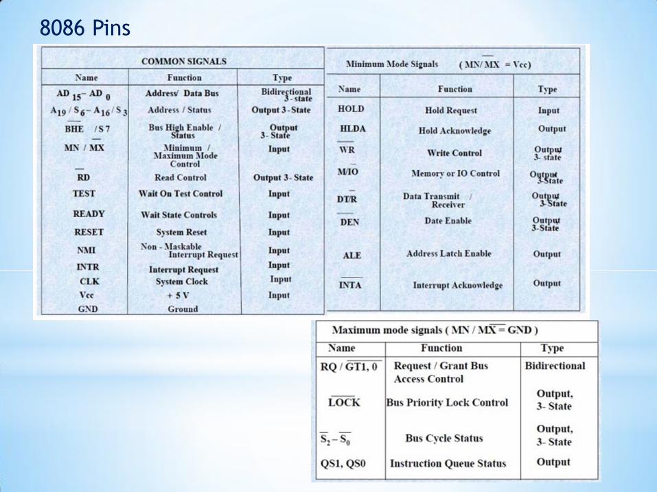
8086 Pins
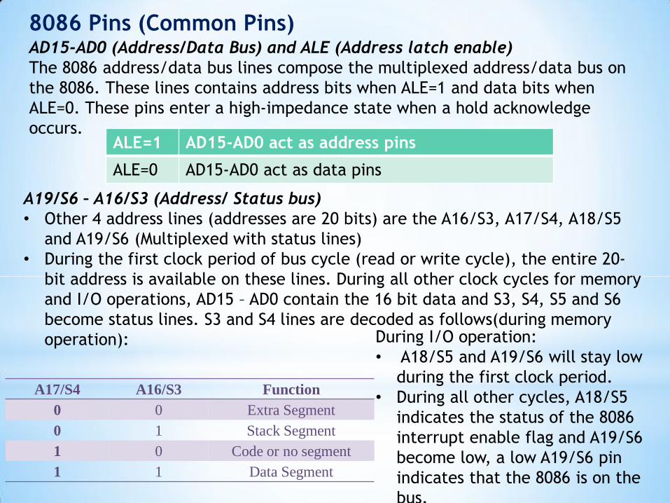
8086 Pins (Common Pins) AD15-AD0 (Address/Data Bus) and ALE (Address latch enable)
The 8086 address/data bus lines compose the multiplexed address/data bus on
the 8086. These lines contains address bits when ALE=1 and data bits when
ALE=0. These pins enter a high-impedance state when a hold acknowledge
occurs. ALE=1 AD15-AD0 act as address pins
ALE=0 AD15-AD0 act as data pins
A19/S6 – A16/S3 (Address/ Status bus)
• Other 4 address lines (addresses are 20 bits) are the A16/S3, A17/S4, A18/S5
and A19/S6 (Multiplexed with status lines)
• During the first clock period of bus cycle (read or write cycle), the entire 20-
bit address is available on these lines. During all other clock cycles for memory
and I/O operations, AD15 – AD0 contain the 16 bit data and S3, S4, S5 and S6
become status lines. S3 and S4 lines are decoded as follows(during memory
operation):
A17/S4 A16/S3 Function
0 0 Extra Segment
0 1 Stack Segment
1 0 Code or no segment
1 1 Data Segment
During I/O operation:
• A18/S5 and A19/S6 will stay low
during the first clock period.
• During all other cycles, A18/S5
indicates the status of the 8086
interrupt enable flag and A19/S6
become low, a low A19/S6 pin
indicates that the 8086 is on the
bus.
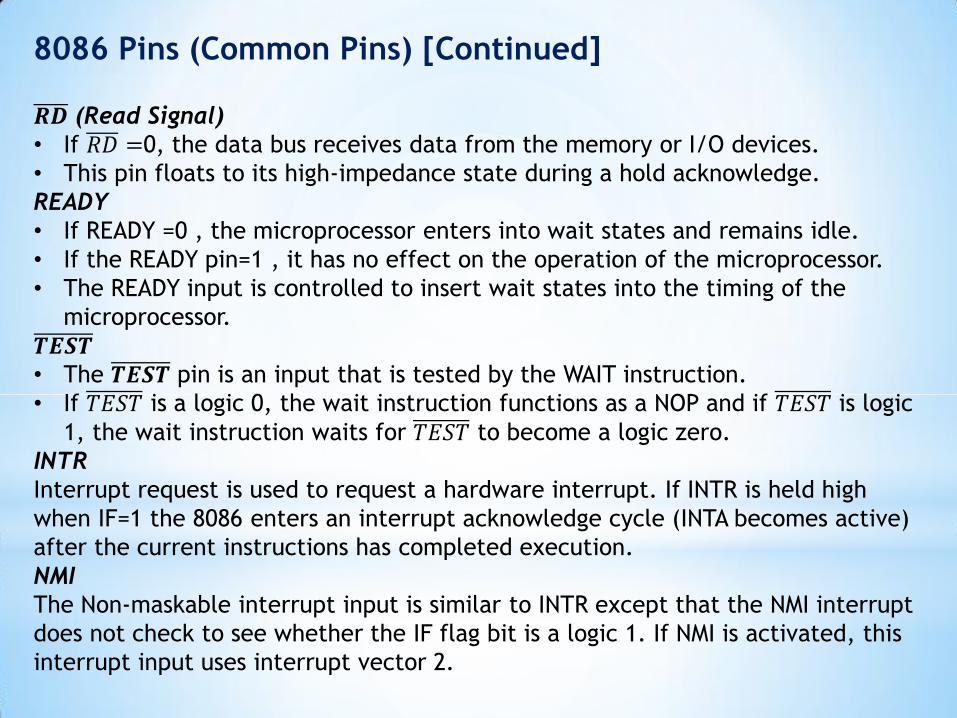
𝑹𝑫 (Read Signal)
• If 𝑅𝐷 =0, the data bus receives data from the memory or I/O devices.
• This pin floats to its high-impedance state during a hold acknowledge.
READY
• If READY =0 , the microprocessor enters into wait states and remains idle.
• If the READY pin=1 , it has no effect on the operation of the microprocessor.
• The READY input is controlled to insert wait states into the timing of the
microprocessor.
𝑻𝑬𝑺𝑻
• The 𝑻𝑬𝑺𝑻 pin is an input that is tested by the WAIT instruction.
• If 𝑇𝐸𝑆𝑇 is a logic 0, the wait instruction functions as a NOP and if 𝑇𝐸𝑆𝑇 is logic
1, the wait instruction waits for 𝑇𝐸𝑆𝑇 to become a logic zero.
INTR
Interrupt request is used to request a hardware interrupt. If INTR is held high
when IF=1 the 8086 enters an interrupt acknowledge cycle (INTA becomes active)
after the current instructions has completed execution.
NMI
The Non-maskable interrupt input is similar to INTR except that the NMI interrupt
does not check to see whether the IF flag bit is a logic 1. If NMI is activated, this
interrupt input uses interrupt vector 2.
8086 Pins (Common Pins) [Continued]
RESET
The RESET input causes the microprocessor to reset itself if this pin is held high
for a minimum of four clocking period. It causes the 8086 to initialize register DS,
SS, ES, IP and flags to all zeros and CS to FFFFH.
CLK
The CLK (clock) pin provides the basic timing signal to the microprocessor. The
clock must have a duty cycle of 33% (high for one third of the clocking period and
low for two thirds) to provide proper internal timing for the 8086.
Vcc
The power supply input provides a +5.0 V, ±10% signal to the microprocessor.
GND
The ground connection is the return for the power supply. Note that the 8086
microprocessors have two pins leveled GND- both must be connected to the
ground for the proper operation.
MN/𝑴𝑿
The minimum/maximum mode pin selects either minimum mode or maximum
mode operation for the microprocessor. If minimum mode is selected, the
MN/𝑀𝑋 pin must be connected directly to +5.0 V.
𝑩𝑯𝑬/𝑺𝟕 (Bus High Enable)
The 8086 outputs a low on this pin during read, write and interrupt acknowledge
cycles in which data are to be transferred in a high order byte (AD15-AD8) of the
data bus. The state of S7 is always logic 1.
8086 Pins (Common Pins) [Continued]
8086 Pins (Minimum Mode Pins)
M/𝑰𝑶
• This pin selects memory or I/O.
• When the 8086 executes an I/O instruction such as IN or OUT, it outputs a LOW
on M/IO .
• On the other hand, the 8086 outputs HIGH on the pin when it executes a
memory reference instruction such as MOV AX, [SI].
𝑾𝑹
When 𝑾𝑹 =0, the processor is performing a write memory or write I/O operation
depending on the M/𝑰𝑶 signal.
𝑰𝑵𝑻𝑨
• The interrupt acknowledge signal is a response to the INTR input pin.
• The 𝑰𝑵𝑻𝑨 pin is normally used to gate the interrupt vector number onto the
data bus in response to an interrupt request.
ALE (Address latch enable)
Used to multiplex the AD0-AD15 into A0-A15 (when ALE=1)and D0-D15 (when
ALE=0).
𝑫𝑻/𝑹 (Data Transmit/receive)
The data transmit/receive signal shows that the microprocessor data bus is
transmitting (𝑫𝑻/𝑹 =1) or receiving (𝑫𝑻/𝑹 = 𝟎) data. The signal is used to
enable external data bus buffers.
DEN (Data bus enable)
Data bus enable activates external data bus buffers. (e.g. Data bus buffer of
8255A)
HOLD
• If the HOLD signal is a logic 1, the microprocessor stops executing software
and places its address, data, and control bus at the high impedance state.
• If the HOLD pin is logic 0, the microprocessor executes software normally.
HALDA (Hold Acknowledgement)
Hold acknowledgement indicates that the 8086 has entered the hold state.
8086 Pins (Minimum Mode Pins) [Continued]
8086 Maximum Mode Pins
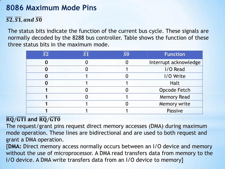
𝑺𝟐, 𝑺𝟏, 𝒂𝒏𝒅 𝑺𝟎
The status bits indicate the function of the current bus cycle. These signals are
normally decoded by the 8288 bus controller. Table shows the function of these
three status bits in the maximum mode.
𝑺𝟐 𝑺𝟏 𝑺𝟎 Function
0 0 0 Interrupt acknowledge
0 0 1 I/O Read
0 1 0 I/O Write
0 1 1 Halt
1 0 0 Opcode Fetch
1 0 1 Memory Read
1 1 0 Memory write
1 1 1 Passive
𝐑𝐐/𝐆𝐓𝐈 and 𝐑𝐐/𝐆𝐓𝟎
The request/grant pins request direct memory accesses (DMA) during maximum
mode operation. These lines are bidirectional and are used to both request and
grant a DMA operation.
[DMA: Direct memory access normally occurs between an I/O device and memory
without the use of microprocessor. A DMA read transfers data from memory to the
I/O device. A DMA write transfers data from an I/O device to memory]
𝑳𝑶𝑪𝑲
The 8086 outputs LOW on the 𝐿𝑂𝐶𝐾 pin to prevent other bus masters from
gaining control of the system bus.
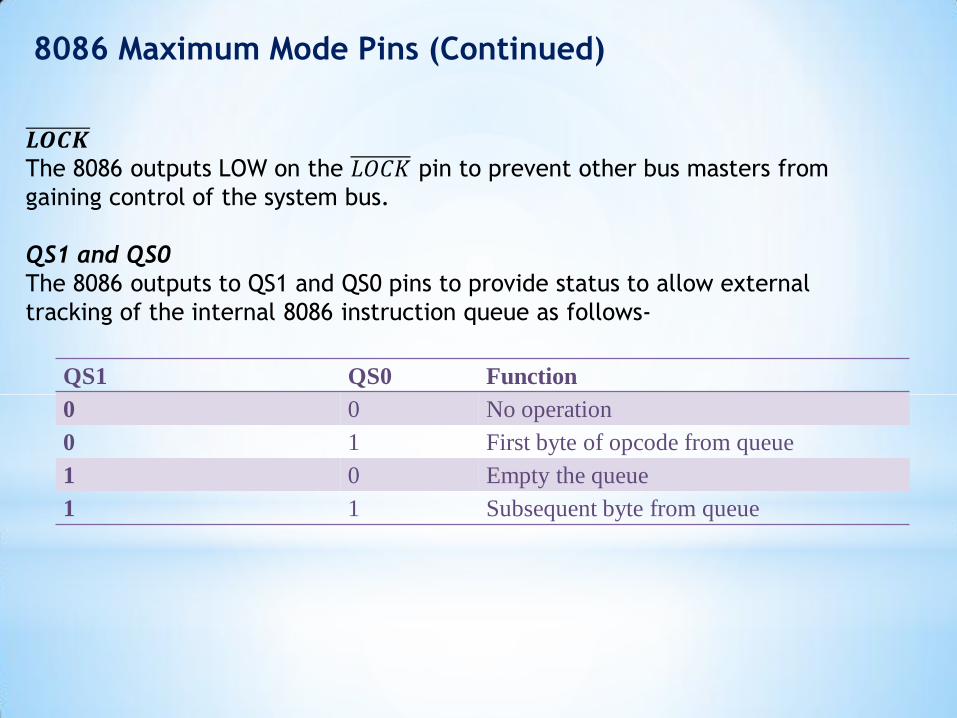
QS1 and QS0
The 8086 outputs to QS1 and QS0 pins to provide status to allow external
tracking of the internal 8086 instruction queue as follows-
QS1 QS0 Function
0 0 No operation
0 1 First byte of opcode from queue
1 0 Empty the queue
1 1 Subsequent byte from queue
8086 Maximum Mode Pins (Continued)
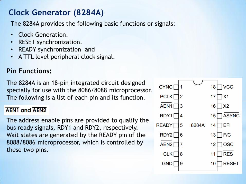
Clock Generator (8284A)
The 8284A provides the following basic functions or signals:
• Clock Generation.
• RESET synchronization.
• READY synchronization and
• A TTL level peripheral clock signal.
Pin Functions:
The 8284A is an 18-pin integrated circuit designed
specially for use with the 8086/8088 microprocessor.
The following is a list of each pin and its function.
The address enable pins are provided to qualify the
bus ready signals, RDY1 and RDY2, respectively.
Wait states are generated by the READY pin of the
8088/8086 microprocessor, which is controlled by
these two pins.
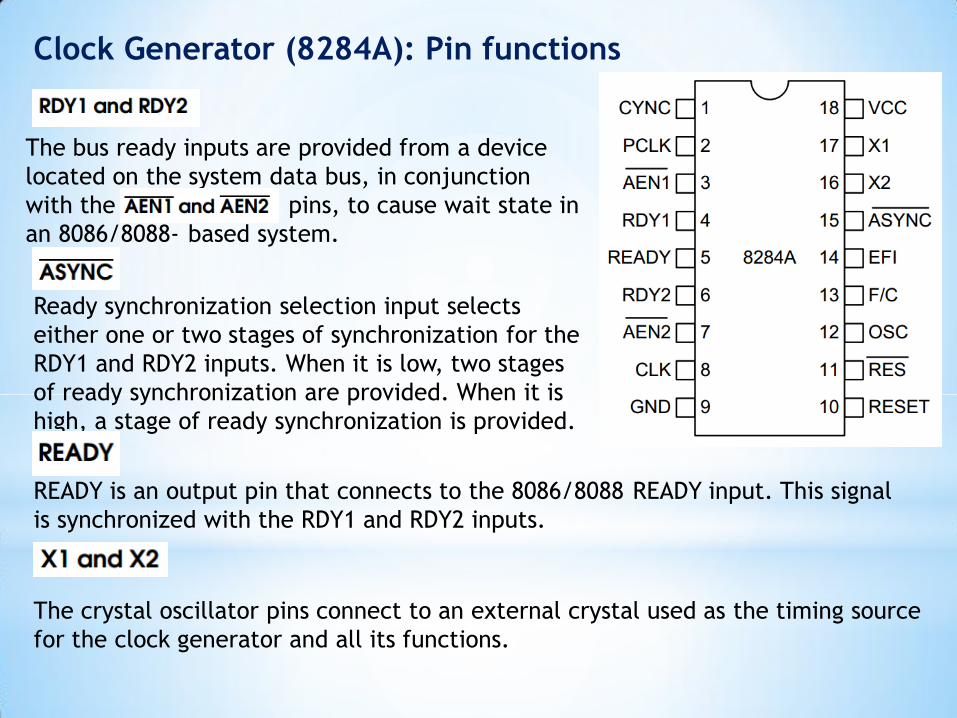
Clock Generator (8284A): Pin functions
The bus ready inputs are provided from a device
located on the system data bus, in conjunction
with the , pins, to cause wait state in
an 8086/8088- based system.
Ready synchronization selection input selects
either one or two stages of synchronization for the
RDY1 and RDY2 inputs. When it is low, two stages
of ready synchronization are provided. When it is
high, a stage of ready synchronization is provided.
READY is an output pin that connects to the 8086/8088 READY input. This signal
is synchronized with the RDY1 and RDY2 inputs.
The crystal oscillator pins connect to an external crystal used as the timing source
for the clock generator and all its functions.
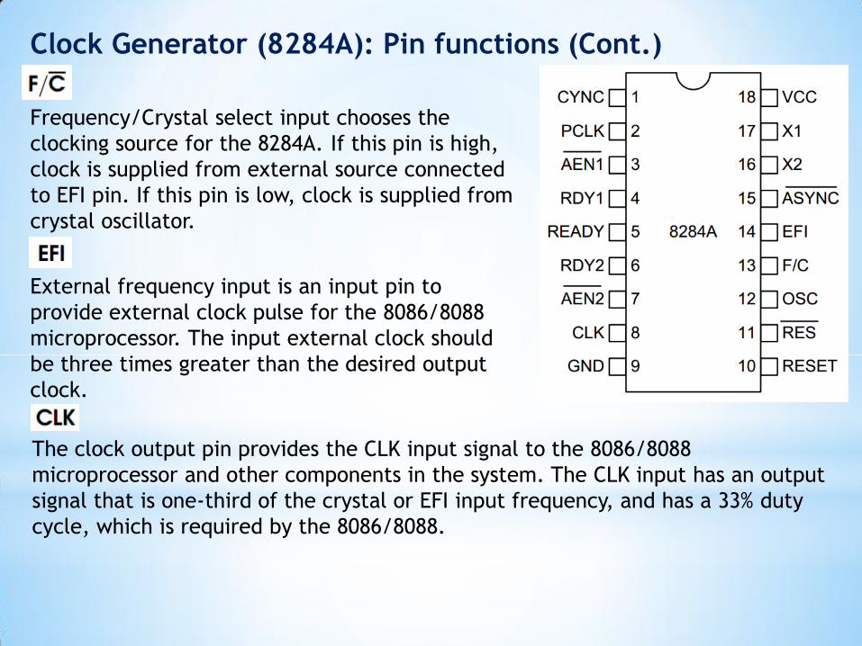
Clock Generator (8284A): Pin functions (Cont.)
Frequency/Crystal select input chooses the
clocking source for the 8284A. If this pin is high,
clock is supplied from external source connected
to EFI pin. If this pin is low, clock is supplied from
crystal oscillator.
External frequency input is an input pin to
provide external clock pulse for the 8086/8088
microprocessor. The input external clock should
be three times greater than the desired output
clock.
The clock output pin provides the CLK input signal to the 8086/8088
microprocessor and other components in the system. The CLK input has an output
signal that is one-third of the crystal or EFI input frequency, and has a 33% duty
cycle, which is required by the 8086/8088.
Clock Generator (8284A): Pin functions (Cont.)
The peripheral clock signal is one-sixth the crystal or EFI input frequency, and has
a 50% duty cycle. The PCLK output provides a clock signal to the peripheral
equipment in the system.
The oscillator output is a TTL-level signal that is at the same frequency as the
crystal. The OSC output provides an EFI input to other 8284A clock generators in
some multiple processor system.
The reset input is an active low input to the 8284A which is used to generate
RESET signal of microprocessor.
The reset output is connected to the 8086/8088 RESET input pin.
The clock synchronization pin is used whenever the EFI input provides
synchronization in systems with multiple processor. If the internal crystal
oscillator is used, this pin must be grounded.
GND is connected to ground and Vcc to +5V with tolerance of ±10%
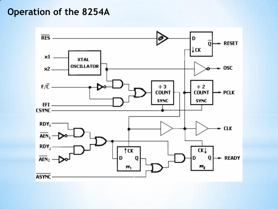
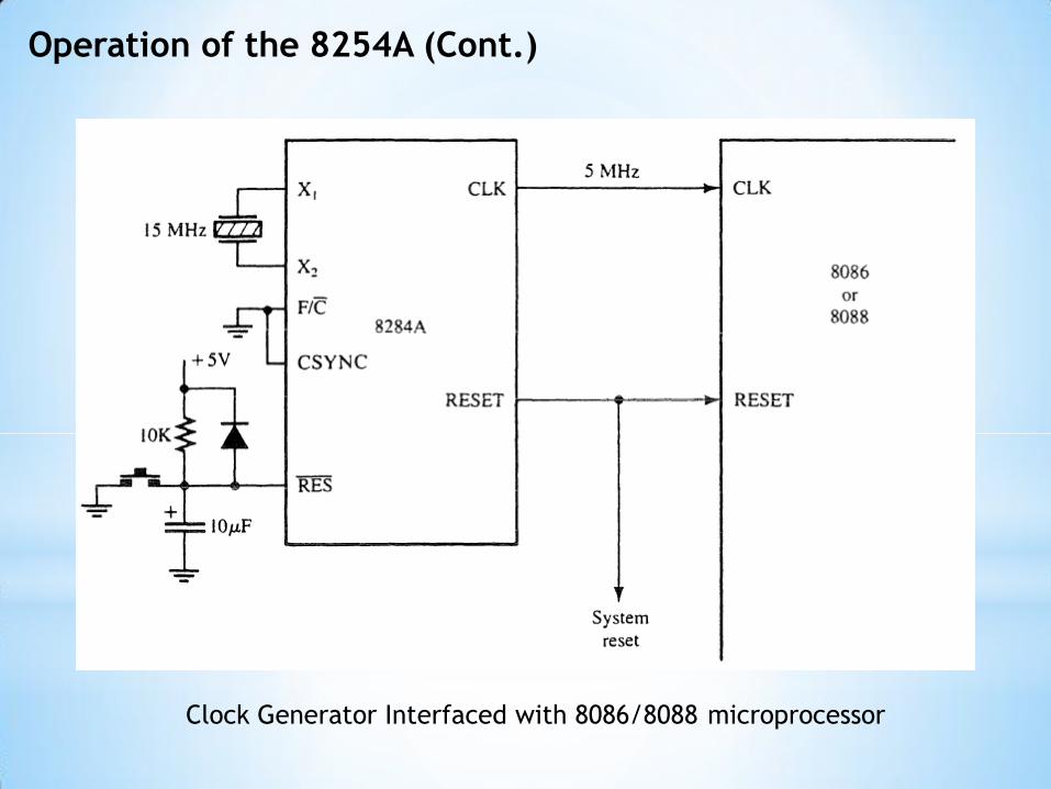
Operation of the 8254A
Operation of the 8254A (Cont.)
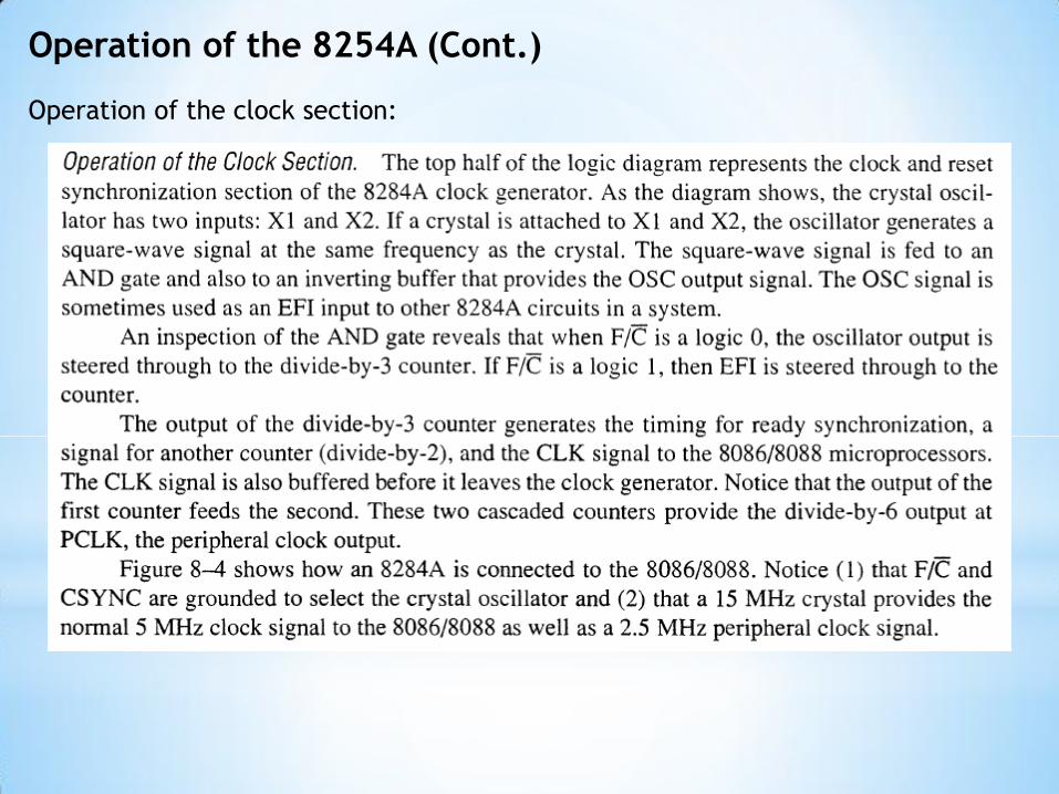
Operation of the clock section:
Operation of the 8254A (Cont.)
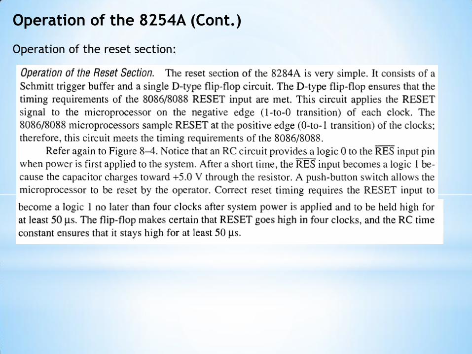
Operation of the reset section:
Operation of the 8254A (Cont.)
Clock Generator Interfaced with 8086/8088 microprocessor