Embed Size (px)
Citation preview
NETAJI SUBHAS INSTITUTE OFTECHNOLOGY
8085 MORSE CODE TUTOR
TEAM:Arushi-36/EC/13Ashima-37/EC/13
FACULTY:Prof. D.V Gadre
ELECTRONICS AND COMMUNICATION DEPARTMENT
June 9, 2016
ii
Acknowledgements
Firstly we would like to thank Prof. Dhananjay Gadre for his unconditionalsupport and thorough guidance without which this project would not haveseen the light of the day. He not only guided us through the project but alsoplayed a vital role in helping us relate the theoretical concepts with theirpractical concepts and instilled in us enthusiasm to learn more about thisfield.
We would also like to thank specially Gaurav Tyagi and Anshuman Mishrafor motivating us and for helping us a lot in finalizing this project within thelimited time frame and our fellow classmates Abhishek Pandey,Arun Ku-mar, Ankush and Sachin among a few others who provided immeasurablehelp during the process.
iii
Contents
Acknowledgements iii
1 SYNOPSIS 11.1 PROJECT DESCRIPTION . . . . . . . . . . . . . . . . . . . . 11.2 BLOCK DIAGRAM . . . . . . . . . . . . . . . . . . . . . . . . 11.3 INPUTS . . . . . . . . . . . . . . . . . . . . . . . . . . . . . . . 21.4 OUTPUTS . . . . . . . . . . . . . . . . . . . . . . . . . . . . . 31.5 BOARD LAYOUT . . . . . . . . . . . . . . . . . . . . . . . . . 41.6 SCHEMATIC . . . . . . . . . . . . . . . . . . . . . . . . . . . 51.7 CODE FLOW DIAGRAM . . . . . . . . . . . . . . . . . . . . 61.8 TESTING AND DEBUGGING . . . . . . . . . . . . . . . . . . 61.9 PROBLEMS FACED . . . . . . . . . . . . . . . . . . . . . . . 7
8

iv
1
Chapter 1
SYNOPSIS
1.1 PROJECT DESCRIPTION
The microprocessor will generate Morse code of alphabets and numbers.It will teach as well as test user’s proficiency. The first two modes will beteaching mode and the remaining three will be testing mode. Modes are asfollows:
• Teaching mode- Microprocessor will convert each character and num-ber to its corresponding Morse code signals which are output throughbuzzer and display it on LCD .The speed of generating Morse code orwords per minute will depend on the speed set by user.
◦ Mode 1- Morse code of numbers from 0 to 9 would be generatedrepeatedly.
◦ Mode 2- Morse code of alphabets would be generated repeatedly.
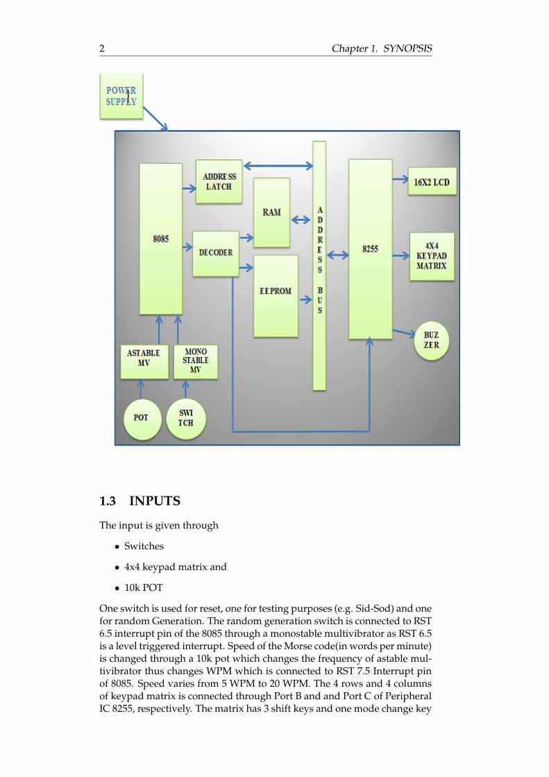
• Testing mode – A random Morse code signal will be generated anduser will input his response through 4x4 keypad matrix (using shiftkey combinations) which has 16 keys including 3 shift keys, a modechange key, and 12 alphabets and numbers keys .The response will beevaluated and result will be displayed on LCD.
◦ Mode3- A code will be generated to test the users on what theyhave learnt in mode 1.
◦ Mode 4- A code will be generated to test the users on what theyhave learnt in mode 2.
◦ Mode 5- A comprehensive and complete evaluation of user’sknowledge of Morse code will be done.
1.2 BLOCK DIAGRAM
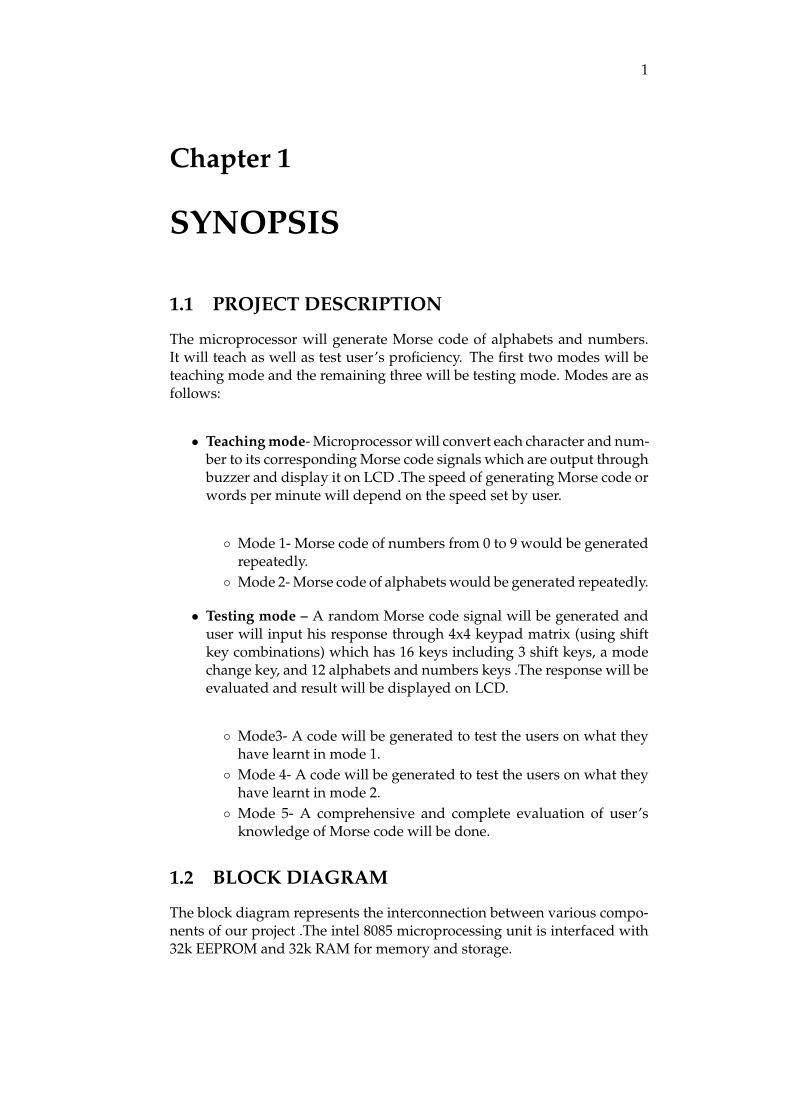
The block diagram represents the interconnection between various compo-nents of our project .The intel 8085 microprocessing unit is interfaced with32k EEPROM and 32k RAM for memory and storage.
2 Chapter 1. SYNOPSIS
1.3 INPUTS
The input is given through
• Switches
• 4x4 keypad matrix and
• 10k POT
One switch is used for reset, one for testing purposes (e.g. Sid-Sod) and onefor random Generation. The random generation switch is connected to RST6.5 interrupt pin of the 8085 through a monostable multivibrator as RST 6.5is a level triggered interrupt. Speed of the Morse code(in words per minute)is changed through a 10k pot which changes the frequency of astable mul-tivibrator thus changes WPM which is connected to RST 7.5 Interrupt pinof 8085. Speed varies from 5 WPM to 20 WPM. The 4 rows and 4 columnsof keypad matrix is connected through Port B and and Port C of PeripheralIC 8255, respectively. The matrix has 3 shift keys and one mode change key
1.4. OUTPUTS 3
and 12 Number and alphabet keys. Shift 1 key with the other 12 keys givenumbers, shift 2 key gives Alphabets from A to L and shift 3 key gives M toX.
1.4 OUTPUTS
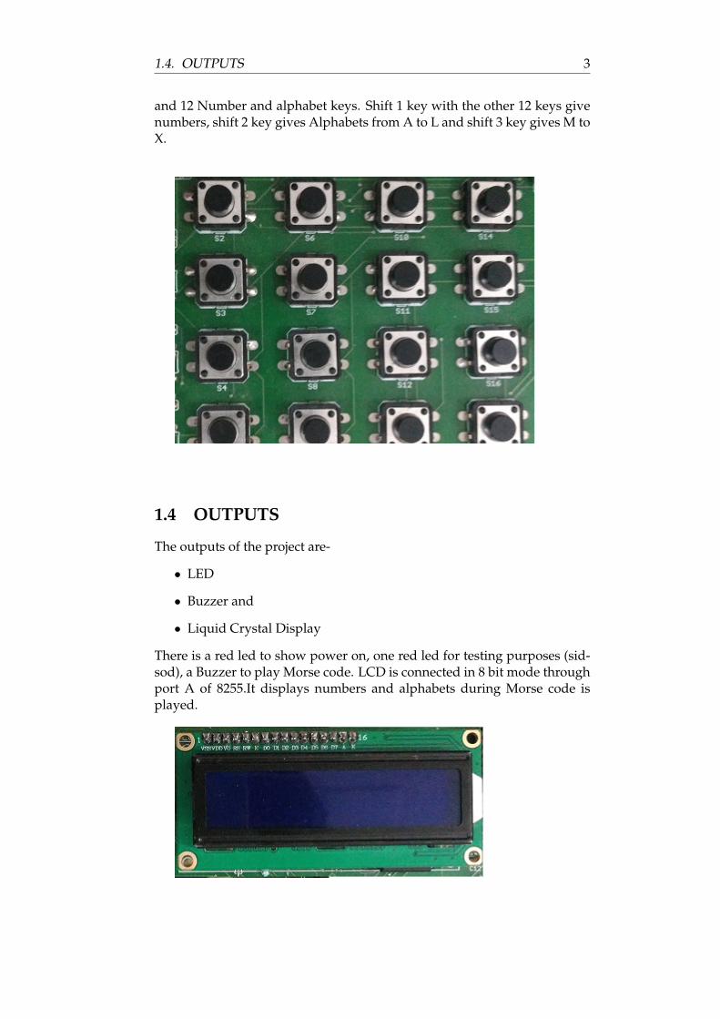
The outputs of the project are-
• LED
• Buzzer and
• Liquid Crystal Display
There is a red led to show power on, one red led for testing purposes (sid-sod), a Buzzer to play Morse code. LCD is connected in 8 bit mode throughport A of 8255.It displays numbers and alphabets during Morse code isplayed.
4 Chapter 1. SYNOPSIS
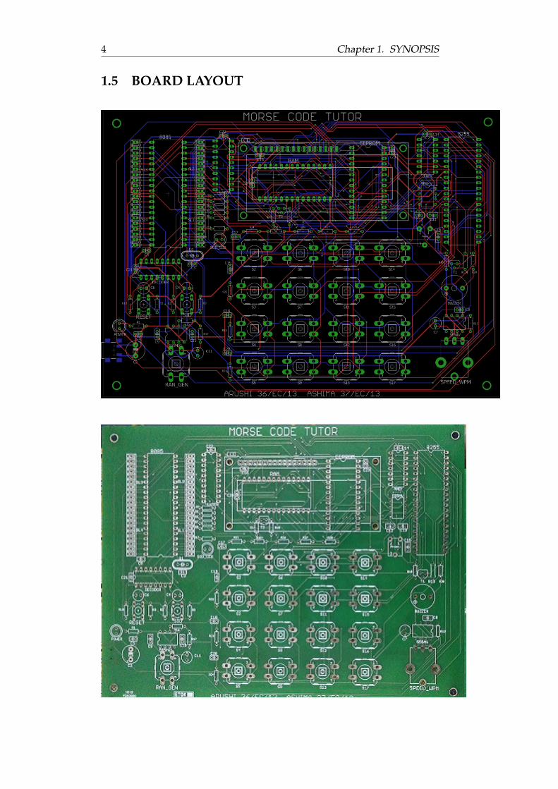
1.5 BOARD LAYOUT
1.6. SCHEMATIC 5
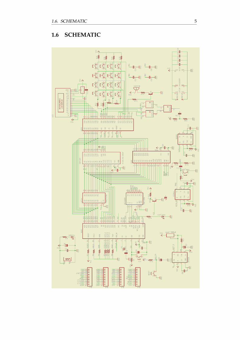
1.6 SCHEMATIC
6 Chapter 1. SYNOPSIS
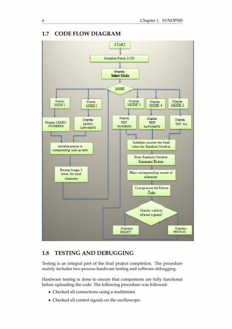
1.7 CODE FLOW DIAGRAM
1.8 TESTING AND DEBUGGING
Testing is an integral part of the final project completion. The proceduremainly includes two process hardware testing and software debugging.
Hardware testing is done to ensure that components are fully functionalbefore uploading the code. The following procedure was followed-
• Checked all connections using a multimeter.
• Checked all control signals on the oscilloscope.
1.9. PROBLEMS FACED 7
• Checked switches using multimeter before soldering them.
• Tested the SID-SOD program using RAM AND EEPROM both.
• Tested the Ports of 8255.
• Checked control signals at interrupt pins of 8085.
• Tested LCD and Buzzer.
Once hardware testing was done, software debugging was done by check-ing fragments of code. The procedure became more difficult and complexin case when there were too many interrupt service routines
1.9 PROBLEMS FACED
• Delay due to faulty EEPROM and RAM- The EEPROM was faulty,we got to know this when we tested SID/SOD code . And then weobserved that our program was not able to return from subroutine be-cause the address of next instruction was not pushed into thev stack,thus we came to the conclusion that RAM is not working.
• Pulse width of monostable multivibrator- The pulse width of MVwhich is connected to RST 6.5 of the microprocessor pin was 200ms,due to which microprocessor was not able to come out of ISR. Thento reduce pulse to 10us a resistor and capacitor was soldered to makea differentiator circuit.
• Problem due to lot of interrupts- This project had 3 interrupts, Key-pad matrix was connected to RST 5.5 pin of microprocessor. We werenot able to detect switches correctly. So, finally we decided to pollkeypad.
8 Chapter 1. SYNOPSIS
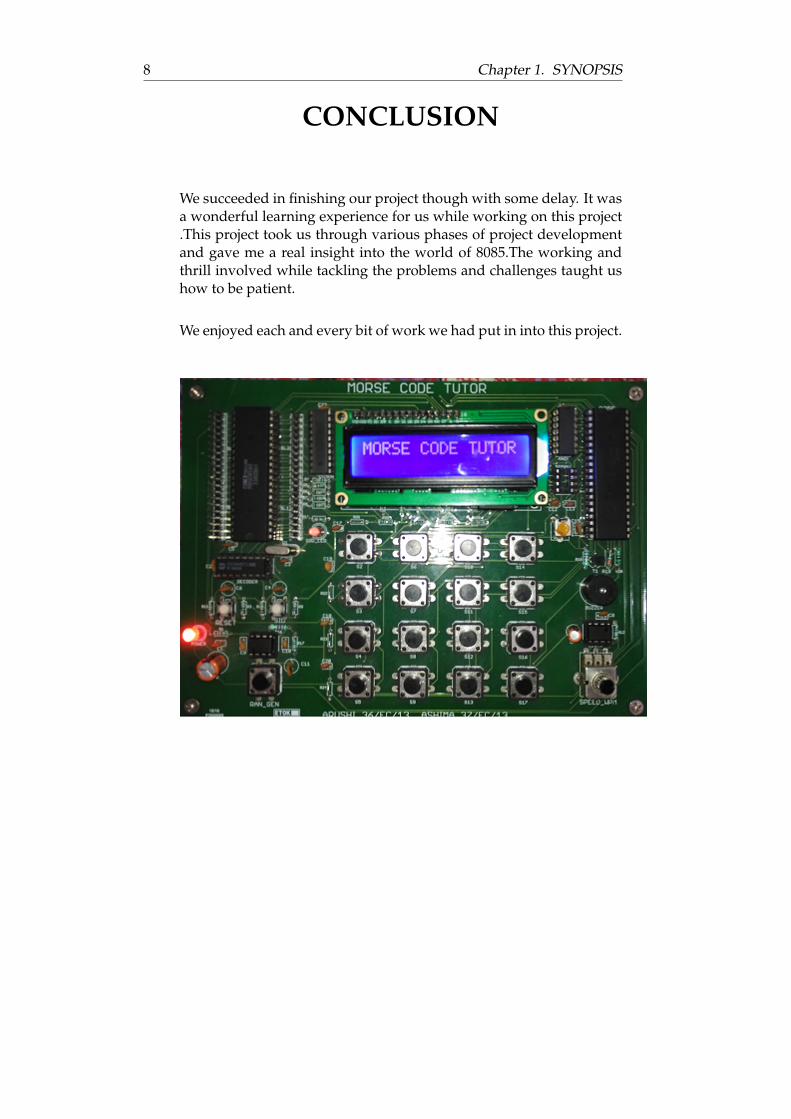
CONCLUSION
We succeeded in finishing our project though with some delay. It wasa wonderful learning experience for us while working on this project.This project took us through various phases of project developmentand gave me a real insight into the world of 8085.The working andthrill involved while tackling the problems and challenges taught ushow to be patient.
We enjoyed each and every bit of work we had put in into this project.
1.9. PROBLEMS FACED 9
BIBLIOGRAPHY
◦ Ramesh S. Gaonkar: “Microprocessor Architecture, Programming,and applications with the 8085”
◦ www.alldatasheet.com
◦ www.sparkfun.com
◦ www.books.google.co.in
◦ www.electronics-tutorials


![Android Interactive Learning Morse App [Learn Morse] Morse Detailed Insrtuctions.pdfAndroid Interactive Learning Morse App [Learn Morse] Version v1.0 - April 2015 Introduction: Caution!](https://img.pdfslide.us/doc/110x75/5f2e43e86c3c8526ba625367/android-interactive-learning-morse-app-learn-morse-morse-detailed-android-interactive.jpg)