Embed Size (px)
Citation preview

Modicon TSX Compact (A120)Modular Programmable ControllerComponents for Railway Train Applications
User Manual
802 BHB 009 00 Date 05/96 22
Translation of the German Description802 BHB 009 02 (A91M.12--700 019.22)

20ii
Notes
Application Note
Caution The relevant regulations must be observed for control applications in-volving safety requirements.For reasons of safety and to ensure compliance with documented system data,repairs to components should be performed only by the manufacturer.
TrainingAEG Schneider Automation offers suitable training that provides further informationconcerning the system (see addresses).
Data, Illustrations, AlterationsData and illustrations are not binding. We reserve the right to alter our products in linewith our policy of continuous product development. If you have any suggestions for im-provements or amendments or have found errors in this publication, please notify us byusing the form on the last page of this publication.
AddressesThe addresses are given at the end of this publication.
CopyrightAll rights reserved. No part of this document may be reproduced or transmitted in anyform or by any means, electronic or mechanical, including copying, processing or anyinformation storage, without permission in writing by the AEG Schneider Automation.You are not authorized to translate this document into any other language.
TrademarksAll terms used in this user manual to denote AEG Schneider Automation products aretrademarks of the AEG Schneider Automation GmbH.
© 1996 AEG Schneider Automation.

20 iii
Terminology
Note This symbol emphasizes very important facts.
Caution This symbol refers to frequently appearing error sources.
Warning This symbol points to sources of danger that may cause financial andhealth damages or may have other aggravating consequences.
Expert This symbol is used when a more detailed information is given, which is in-tended exclusively for experts (special training required). Skipping this information doesnot interfere with understanding the publication and does not restrict standard applica-tion of the product.
Path This symbol identifies the use of paths in software menus.
Figures are given in the spelling corresponding to international practice and approvedby SI (Système International d‘ Unités).I.e. a space between the thousands and the usage of a decimal point (e.g.: 12 345.67).

20iv
Objectives
This manual is a supplement to the user manual for Compact TSX (A120). It describesthe components developed specifically for the railway train applications of the A120 andwhich have the following alterations in comparison to the standard modules:
Temperature range continuous operation: --25 ... +70 oCoperation </= 10 min.: --30 ... +85 oC
Supply 24 VDC, +/--5 %
Schock, Vibration according to LES--DB
LEDs green replaced by yellow
Related Documents
Catalogue Programmable Controller A120Product Family ModiconA91V.05-234 836
General Manual A120DIN--Rail Mount Controller(Basic Document)User ManualA91M.12-271 629
Software Dolog AKF→ A120 (AKF12) and A120, Dolog AKFSoftware-Kit Standard Function BlocksE-Nr. 424 271 521 Block Library
A91M.12-703 265
or
Dolog AKF→ A120 / A250 and A120, Dolog AKF(AKF125) Standard Function BlocksSoftware-Kit Block LibraryE-Nr. 424 275 182 A91M.12-703 265

20 Table of Contents v
Table of Contents
Appendix A Module Descriptions 1. . . . . . . . . . . . . . . . . . . . . . . . . . . . . . . . . . . . . . . . . . . .
ADU 254, Analog Inputs 3. . . . . . . . . . . . . . . . . . . . . . . . . . . . . . . . . . . . . . . . . . . . . . . . . . . . . .ADU 256, Analog Inputs 13. . . . . . . . . . . . . . . . . . . . . . . . . . . . . . . . . . . . . . . . . . . . . . . . . . . .ALU 252, Central Processing Unit 25. . . . . . . . . . . . . . . . . . . . . . . . . . . . . . . . . . . . . . . . . . . .DAP 250, DAP 258, Discrete Inputs and Outputs 39. . . . . . . . . . . . . . . . . . . . . . . . . . . . . . .DAP 252, DAP 253, Discrete Inputs and Outputs 49. . . . . . . . . . . . . . . . . . . . . . . . . . . . . . .DAU 252, Analog Output 59. . . . . . . . . . . . . . . . . . . . . . . . . . . . . . . . . . . . . . . . . . . . . . . . . . . .DEP 254, Discrete Input 67. . . . . . . . . . . . . . . . . . . . . . . . . . . . . . . . . . . . . . . . . . . . . . . . . . . .DEP 255, DEP 257, Function 73. . . . . . . . . . . . . . . . . . . . . . . . . . . . . . . . . . . . . . . . . . . . . . . .DNP 255, Power supply 79. . . . . . . . . . . . . . . . . . . . . . . . . . . . . . . . . . . . . . . . . . . . . . . . . . . . .
Index 85. . . . . . . . . . . . . . . . . . . . . . . . . . . . . . . . . . . . . . . . . . . . . . . . . . . . . . . . .

20Table of Contentsvi

22 1
Appendix AModule Descriptions
The module descriptions are arranged alphabetically according to theirabbreviations.

222

20 ADU 214 3
ADU 214Analog InputsModule Description
The analog/digital converter of the ADU 214 module works according tothe principle of integrated conversion procedure (dual slope) with fastback-integration. It is used for measuring analog data providing up to 8non-isolated inputs. The main characteristics are:
four analog inputs, 4-pole (temperature or resistance)Alternatively these inputs can be used for 2-pole voltage measure-ment. Thus it is possible to choose between up to 8 unipolar voltageinputs or up to 4 bipolar voltage inputs. (or combinations of both)
several measuring ranges with a resolution of 15 bit + arithm. sign:
Voltage measurement 0 ... 0.5, 0 ... 1, 0 ... 5, 0 ... 10 V,0.1 ... 0.5, 0.2 ... 1, 1 ... 5, 2 ... 10 V,+0.5, +1, +5, +10 V
current measurement with 0 ... 5, 0 ... 10, 0 ... 20 mA,externalprecision resistance 1 ... 5, 2 ... 10, 4 ... 20 mA,
+5, +10, +20 mATemperature measurement --160/-60 ... +160 oC, resolution <0.02 oC
--200 ... +320 oC, resolution <0.04 oC--200 ... +640 oC, resolution <0.08 oC
Resistance measurement 0 ... 100, 0 ... 200, 0 ... 500 Ω,0 ... 1000, 0 ... 2000 Ω
Broken wire testing of all 4-pole lines. Self calibration using built-in ref-erence resistances andreference voltages. Characteristic curve linea-rizing for platinum and nickel reference resistances according toIEC 751 / DIN 43 760 (Pt 100 ...1000, Ni 100 ...1000).

20ADU 2144
1
2
3
4
5
6
7
8
9
10
11
12
13
14
15
16
17
18
19
20
21
22
Figure 1 Front view and fill-in-label of ADU 214 module
1 General Characteristics
Measuring ranges for voltage, current, temperature and resistancecan be set indivi-dually for each input via control bytes from the CPU of the controller.
Noise suppression can be switched from 50 Hz to 60 Hz.
Analog inputs are scanned cyclically. The PLC accesses the most recently filed valuesasynchronically.
The ADU can be inserted into any slot of subracks DTA 200, 201, 202.
SW-ModulesThe ADU can be used without S/W-Modules.If the additional scaling-modules SKAL and DSKAL are used word-based operationscan directly process the measured values.The module GRENZ provides boundary value control for the upper and lower bounda-ries (of words).

20 ADU 214 5
1.1 Physical Characteristics
The module resides in a standard housing. It provides a backplane bus system and pe-ripheral connections on the front. Screw/plug-in terminal blocks support process signalconnection.
One of the included fill-in-labels can be inserted into the cover of the housing next tothe LED display area. The label has fields which have been prepared for filling in fielddata specifications like signalnames.
1.2 Mode of Functioning
2 of 8 Input Circuits
2120191817161514
109876543
12
1213
11
22
U
U
M
M
7, 8
5, 6
3, 4
1, 2
GN ”U”
+15 V
0 V
--15 V
--
--
GN ”ready”
TOTUSNPAB
PAB
MUX
--15 V +15 V
RAM
80C31
+
--
+15 V
A/D
REF
PAB
PAB+ 5 V
0 V
AGND
Figure 2 Schematic circuit diagram of ADU 214

20ADU 2146
2 Elements for Operation and Display
The front side of the ADU contains the following status displays:
1 green LED ”U” indicating 24 V power statuson: power supply availableoff : power failure
1 green LED ”ready” indicating processor statuson: processor runningoff : processor failure
At initial startup a DIP-switch has to be set. For details see page 11.
3 Configuration
For selecting your configuration consider the following points:
Number of I/O drop (see user manual, chapter 3 ”Equipment list...”).The module does not contain any hardware for setting the node number
Measuring range selection and error analysis (see 3.1)
Noise suppression (see 3.2)
Fritting procedure of the connections 3.3)
Cable connections (cable rooting, shielding, see 3.4)
Assignment of connections and signal addresses (see 3.5)
Representation of peripheral signal connections (DIN A3 forms, see 3.6)
3.1 Measuring range selection and error analysis
3.1.1 Measuring range selectionMeasuring either current or voltage input depends on the type of connector used (i.e.with or without measuring resistance). The appropriate measuring range is selected in-dividuallyfor each input via AKF-software in operand QBx.1 ... QBx.81). The selectedvalue can be changed at random during operation.
Default positions for QBx.1 ...QBx.8 are set to ”0”, i.e. allinputs are inactive.
In addition to the default values the following individual settings can be selected:
1) x = node number

20 ADU 214 7
Table 1 QBx.1 ... QBx.8 2)Possible binary settings for voltage and current measuring ranges
Bit 7 Bit 6 Bit 5 Bit 4 Bit 3 Bit 2 Bit 1 Bit 0
0 0 0 0 0 0 0 0 inactive channel
0 0 * * * 0 0 1 10 V0 1 0 5 V0 1 1 1 V / 20 mA 3) / 10 mA 4)
1 0 0 0.5 V / 10 mA 3) / 5 mA 4)
0 0 * * 0 * * * 0 ... 100 % value representation0 * 1 * * * 20 ... 100 % value representation
(with Offset = LIVE-ZERO)
0 0 0 0 * * * * negative values are limited to 01 * * * * negative values are outputted up to
error message --1.6 %
0 0 0 * * * * * up to 8 unipolar inputs1 0 0 * * * up to 4 bipolar inputs
Table 2 Possible binary settings for QBx.1 ... QBx.8 2) for temperature and resistance measuringranges
Bit 7 Bit 6 Bit 5 Bit 4 Bit 3 Bit 2 Bit 1 Bit 0
0 1 0 * * * 0 0 temperature with Ni up to +160 oC0 1 temperature with Pt up to +160 oC1 0 temperature with Pt up to +320 oC1 1 temperature with Pt up to +640 oC
0 1 0 * 0 0 * * detector 100 Ohm0 1 detector 200 Ohm1 0 detector 500 Ohm1 1 detector 1000 Ohm
resistance measuring ranges0 1 1 * 0 0 0 0 0 ... 100 Ohm
0 0 1 0 ... 200 Ohm0 1 0 0 ... 500 Ohm0 1 1 0 ... 1000 Ohm1 0 0 0 ... 2000 Ohm
0 1 * 0 * * * * 4-wire detector1 * * * * 2-wire detector with 10 Ohm
wire extension
2) x = node number3) with measuring resistance 50 Ω4) with measuring resistance 100 Ω

20ADU 2148
Table 3 Possible decimal or hexadecimal settings for QBx.1 ... QBx.8 5) for voltage and current mea-suring ranges.
Content of measuring rangefor IWx.1 ... IWx.8 parametersQBx.1...QBx.8 5)
DEZ HEX
0 0 input is inactive (no conversion)
2-pole unipolar measuring ranges1 1 0 ... 10 V + limit2 2 0 ... 5 V + limit3 3 0 ...1 V / 0 ... 20 mA 6) / 0 ...10 mA 7) + limit4 4 0 ... 0.5 V / 0 ...10 mA 6) / 0 ... 5 mA 7) + limit5 5 - (invalid measuring range): :8 8 -9 9 2 ... 10 V + limit10 A 1 ... 5 V + limit11 B 0.2 ... 1 V / 4 ... 20 mA 6) / 2 ...10 mA 7) + limit12 C 0.1 ... 0.5 V / 2 ...10 mA 6) / 1 ... 5 mA 7) + limit13 D -:16 10 -17 11 0 ... 10 V + limit18 12 0 ... 5 V + limit19 13 0 ... 1 V / 0 ... 20 mA 6) / 0 ...10 mA 7) + limit20 14 0 ... 0.5 V / 0 ...10 mA 6) / 0 ... 5 mA 7) + limit21 15 -:24 18 -25 19 2 ... 10 V + limit26 1A 1 ... 5 V + limit27 1B 0.2 ...1 V / 4 ... 20 mA 6) / 2 ...10 mA 7) + limit28 1C 0.1 ... 0.5 V / 2 ...10 mA 6) / 1 ... 5 mA 7) + limit29 1D -:32 20 -
2-pole bipolar measuring ranges (related inputs must be set to samemeasuring range)33 21 +10 V (+ limit of single input)34 22 +5 V (+ limit of single input)35 23 +1 V / +20 mA 6) / +10 mA 7) (+ limit of single input)36 24 +0.5 V / +10 mA 6) / +5 mA 7) (+ limit of single input)37 25 -:63 3F -
5) x = node number6) with measuring resistance 50 Ω7) with measuring resistance 100 Ω

20 ADU 214 9
Table 4 Possible decimal or hexadecimal QBx.1 ... QBx.8 8) settings for temperature and resistancemeasuring ranges
content of measuring rangefor IWx.1 ... IWx.8 parametersQBx.1...QBx.8 8)
DEZ HEX
4-pole measuring ranges, temperature detector with 4-pole wire connection 9)
64 40 -60 ... +160 oC with Ni 100 IK = 2.5 mA65 41 -160 ... +160 oC with Pt 100 IK = 2.5 mA66 42 -200 ... +320 oC with Pt 100 Ik = 2.5 mA67 43 -200 ... +640 oC with Pt 100 Ik = 2.5 mA68 44 -60 ... +160 oC with Ni 200 Ik = 2.5 mA69 45 -169 ... +160 oC with Pt 200 Ik = 2.5 mA70 46 -200 ... +320 oC with Pt 200 Ik = 2.5 mA71 47 -200 ... +640 oC with Pt 200 Ik = 2.5 mA72 48 -60 ... +160 oC with Ni 500 Ik = 2.5 mA73 49 -160 ... +160 oC with Pt 500 Ik = 2.5 mA74 4A -200 ... +320 oC with Pt 500 Ik = 2.5 mA75 4B -200 ... +640 oC with Pt 500 Ik = 1.5 mA76 4C -60 ... +160 oC with Ni 1000 Ik = 1.5 mA77 4D -160 ... +160 oC with Pt 1000 Ik = 1.5 mA78 4E -200 ... +320 oC with Pt 1000 Ik = 1.5 mA79 4F -200 ... +640 oC with Pt 1000 Ik = 1.5 mA
4-pole measuring ranges, temperature detector with 2-pole wire compensation(10 Ohm) 9)
80 50 -60 ... +160 oC with Ni 100 IK = 2.5 mA81 51 -160 ... +160 oC with Pt 100 IK = 2.5 mA82 52 -200 ... +320 oC with Pt 100 IK = 2.5 mA83 53 -200 ... +640 oC with Pt 100 IK = 2.5 mA84 54 -60 ... +160 oC with Ni 200 IK = 2.5 mA85 55 -160 ... +160 oC with Pt 200 IK = 2.5 mA86 56 -200 ... +320 oC with Pt 200 IK = 2.5 mA87 57 -200 ... +640 oC with Pt 200 IK = 2.5 mA88 58 -60 ... +160 oC with Ni 500 IK = 2.5 mA89 59 -160 ... +160 oC with Pt 500 IK = 2.5 mA90 5A -200 ... +320 oC with Pt 500 IK = 2.5 mA91 5B -200 ... +640 oC with Pt 500 IK = 1.5 mA92 5C -60 ... +160 oC with Ni 1000 IK = 1.5 mA93 5D -160 ... +160 oC with Pt 1000 IK = 1.5 mA94 5E -200 ... +320 oC with Pt 1000 IK = 1.5 mA95 5F -200 ... +640 oC with Pt 1000 IK = 1.5 mA
4-pole measuring ranges for resistance measuring with 4-pole wire 9)
96 60 0 ... 100 Ohm, IK = 2.5 mA97 61 0 ... 200 Ohm, IK = 2.5 mA98 62 0 ... 500 Ohm, IK = 2.5 mA99 63 0 ... 1000 Ohm, IK = 2.5 mA100 64 0 ... 2000 Ohm, IK = 1.5 mA101 65 -:111 6F -
4-pole measuring ranges for resistance measuring with 2-pole wire compensation (10 Ohm) 9)
112 70 0 ... 100 Ohm IK = 2.5 mA113 71 0 ... 200 Ohm IK = 2.5 mA114 72 0 ... 500 Ohm IK = 2.5 mA115 73 0 ... 1000 Ohm IK = 2.5 mA116 74 0 ... 2000 Ohm IK = 1.5 mA117 75 -:255 FF -
8) x = node number9) The referenced input with an odd number has to be set to 0 (inactive) for all 4-pole measuring ranges.

20ADU 21410
Note After system startup a measured value IWx.1 ... IWx.8 10) remains 0, until themodule can be addressed. After that the module displays ”invalid station identification”-32 768 until the value is converted by selecting a valid measuring range (operand)QBx.1 ... QBx.8. This leads to a display of the valid value.Changing that measuring range results in the display ” invalid station identification”-32 768 in the following cycle, until in the subsequent cycle the measured value beco-mes valid after max. 300 ms.
Note In case of 2-polemeasurementUp to a response value of -1.6 % of the rated value negative values in unipolar opera-tion mode and + limit result in a digital value ”0” without causing an error message. Ifmeasured values fall belowthis limit error message SMBx.1 10) = y5 11) (see Table 5)and a measured value IWx.y = -32 767 will be displayed.Negative measuring values in unipolar operation mode and + limit produce a digital va-lue (up to -512) of the referred negative value without error message - up to a re-sponse value of -1.6 % of the rated value. If measured values fall below this limit er-ror message SMBx.1 = y5 (see Table 5) and a measured value IWx.y = -32 767 will bedisplayed.In case of measuring ranges with a 20 % Offset (LIVE-ZERO) the maxixmum re-sponse limit for valued measure underflow is about. 10 % of the rated value. The nega-tiv digital value with + limit can fall to -3 840.
Note 4-pole measurementConstant current only flowswhen measuring with this input. Thus the effective currentfor warming up the reference resistance is smaller. The current, however, dependsupon the number of active inputs. In case of one active input with a 4-pole detectorthe keying ratio is 1: 2. This is because one reference measurement occurs in betweeneach measurement (effective value = IK x 0.71). In case of four active inputs the keyingratio is 1: 5 (effective value = IK x 0.45).
3.1.2 Integration into application programA transfer of operands QBx.1 ... QBx.8 10) to the ADU occurs within each program cy-cle.In constant measuring ranges it is not necessary that the operands QBx.1...QBx.8 beloaded in each program cycle (slowing down of processing time).Therefore when loading you can use the switch-on marker in combination with a jumperoperand, e.g.:
:A SM2:JF =Y1:LD V1 ... 116:= QB2.1
::
:LD V1 ... 116:= QB2.8
Y1 :***
10) x = node number11) y = input number

20 ADU 214 11
3.1.3 Error EvaluationIn case of an ADU error the user-related system marker SMx.1 12) stores a multiad-dress message. Detailed error information can be obtained from operand SMBx.1 .The values in SMBx.1 are constantly updated. If the cycle is error-freethe content of allinputs is deleted. As it is impossible to store errors until they are queried short-term er-rors can be lost if the A120-cycle is slower than the ADU cycle.
The coding of SMBx.1 12) gives the incorrect input accompanied by an error number.
Binary Bit 7 Bit 6 Bit 5 Bit 4 Bit 3 Bit 2 Bit 1 Bit 0data format: input number (1 ... 8) error number (1 ... 7)
hexadecimal y 13) (left digit) n (right digit)data format: input number (1 ... 8) error number (1 ... 7)
input numberShould errors occur simultaneously in several inputs the error with the lowest inputnumber will be displayed until it is debugged. After that the error with the next highestinput numberwill be displayed and so on.
Table 5 Possible error messages
Content of SMBx.1 12)
BIN HEX meaning
0000 0000 00 no errorxxxx 0001 y1 parameter error / invalid measuring rangexxxx 0010 y2 inputs 1, 3, 5, 7 only allow 2-pole measuring.xxxx 0011 y3 at inputs 2, 4, 6, 8 associated inputs 1, 3, 5, 7 must be inactive.xxxx 0100 y4 broke wire detected at 4-pole measuringxxxx 0101 y5 measuring range underflow, detector short-circuit when measuring temperature or
broke wire at Live-Zeroxxxx 0110 y6 measuring range overflowxxxx 0111 y7 in bipolar operating mode both connected inputs must be set to
same measuring range.1111 1111 FF system error or voltage drop / low voltage UB24 results in module
reset and Totmann trash.relations between SM 31 ... 48, SMx.1 und SMBx.1 see Table 6.
When an error has occured the transfered measured value of the inputs concerned isset (IWx.y 12) 13)) to defined constants.
-32 768 inactive input / invalid measuring range / broke wire at four-pole measuring+32 767 measuring range overflow-32 767 measuring range underflow0 parameter error in bipolar operation mode of the corresponding input.
12) x = node number13) y = input number

20ADU 21412
The following relations exist between common system markers SM 31 ... 48 and user-related system markers SMx.1 14) (multiaddress-marker) und SMBx.1 (detail marker):
Table 6 relations between SM 31 ... 48, SMx.1 und SMBx.1 14)
SM31 ... SMx.1 SMBx.1 IWx.1 ... meaningSM48 IWx.8
1 0 00 00 module not plugged in
1 1 00 00 module plugged in, UB = 24 V nonexistent0 0 00 00 module plugged in, AWP running with UB = 24 V
0 1 FF alt module plugged in, AWP running, UB = 24 V switched offagain
1 0 00 00 User program running, UB = 24 V, module removed0 0 00 new User program running, UB = 24 V, module plugged in again
(after about 1 s)
0 1 FF alt module plugged in, AWP running, UB = 24 V switched off
1 0 00 00 User program running, UB = 24 V switched off and moduleremoved
1 0 00 00 User program running, UB = 24 V switched off and moduleplugged in again
14) x = node number

20 ADU 214 13
3.2 Noise Suppression (DIP-switch B1)
The ADU provides a suppression of mains frequencies on the peripheral lines. ADUsare shipped with 50 Hz suppression, which can be switched to 60 Hz with DIP-switchB1.
50 Hz noise suppression(as shipped)
60 Hz noise suppression
see Figure 4
OFF ON
B2
B1
B1
Figure 3 Back view of ADU (Noise suppression)
3.3 Fritting procedure of input connections (DIP-switch B2)
Fritting prevents an increase of transfer resistance on peripheral plug-ins. Fritting is ac-complished by adding voltages >10 V und 0 to the contacts at defined time intervals.The resulting current (flowing for about 1 ms) is limited to <8 mA. The contacts of thecurrent and voltage paths of 4-pole connections automatically receive this load witheach measurement. The contacts of the active voltage inputs are frittedcyclically every30 minutes.The fritting process is switched on and off with DIP-switch B2.
fritting switched off
OFF ON
see Figure 3
fritting switched on(as shipped)
B2
B2
B1
Figure 4 Back view of ADU (fritting connections)

20ADU 21414
3.4 Wiring
Note For general wiring and set-up instructions please refer to youruser manual,chapter 5.2.1 ”Measures Taken Regarding Installation and Wiring”.
Foil-shielded cables (2 x or 4 x 0.5 mm2, twisted per channel) have to be used forconnections. All channels can be run within one joint shielded cable.
If detectors are connected with 4-pole wires, e.g Ni 100, Pt 100, conductors for cur-rent and voltage path must be twisted in pairs.
The connections between the shield and ground must be as closely as possible(<20 cm) at one end. If higher noise levels exist, the cable shield has to be earthedat both ends (see also user manual, chapter 5.2 ”EMC Measures”.
The cable must not be run together with energy supply lines or similar electrical di-sturbers. Distance >0.5 m
3.5 Connection and Signal Address Assignment
1) resistance temperature detector Pt 100 ... 1000, Ni 100 ... 1000 or remote resistance detector0 ... 2000 Ohm
2) external reference resistance 50 or 100 Ohm, 0.1 %, 0.125 W, Tk 253) see chapter 3.5.1, page 13
4) The common reference point ”AGND” is internally connected to 0 V (reference potential of PLC).
2120191817161514
109876543
12
1213
11
22
UBM2
0.16 A
AGND4)
UIWx.2
IWx.4
--+
U
+
--
U --+
I
+
--
IWx.1
IWx.3
109876543
0 ... 10 Ohm
IWx.2
IWx.4
IWx.8
I --+
I
--
--++
--IWx.6
IWx.7
IWx.6
IWx.8 1)
2120191817161514
--++
--+
--+ U
1)
1)
2)
2)
2)
3)
--+ I
2)
Figure 5 Example for wiring of ADU 214
Fill in the signal names or names of the actuators into the label of the module housing.

20 ADU 214 15
You can connect a4-poleresistance detector oder2-poleresistance detector with
10 Ω wiring compensation or2-polevoltage detector unipolar 0 ... 0.5, 0 ... 1, 0 ... 5, 0 ... 10 V,
0.1 ... 0.5, 0.2 ... 1, 1 ... 5, 2 ... 10 V,or2-polevoltage detector bipolar +0.5, + 1, +5, +10 Voder2-polecurrent detector unipolar 0 ... 5, 0 ... 10, 0 ... 20 mA,
1 ... 5, 2 ... 10, 4 ... 20 mA,oder2-polecurrent detector bipolar +5, + 10, +20 mA
The common reference point ”AGND” is internally connected to 0 V (reference potentialof PLC).
Additionally 8 bridges are supplied with the ADU 214 package. Use these, if you haveto short-circuit 2 neighbouring terminal blocks, e.g. when using two-wire resistancetem-perature detectors.
Inputs which are not used have to be set to measuring range ”inactive” (0).By doing so,you avoid error messages and the cycle time of conversion decreases.
After conversion, analog input values are put into input words IWx.1 ... IWx.8.

20ADU 21416
3.5.1 Voltage and Current MeasurementEach 4-pole input can be switched to a 2 x 2-pole unipolar voltage input. In this casethe first input is single-ended and the second input is a differential input.For positive voltages with the same reference point, AGND voltage inputs 1, 3, 5, 7 canbe used as single ended. Inputs 2, 4, 6, 8, can be used as differential inputs for posi-tive or negative voltages. With regard to differential inputs, however, you always haveto take care that voltages on both the positive input and negative inputs must not ex-ceed the common-mode voltage rangeagainst common reference point AGND (UE <+11 V). Therefore, with potential-free detectors there always has to be a reference bet-ween a random point of the circuit and AGND, e.g. as shown in Figure 5 Picture 5,byconnecting the negative input terminal block toAGND. For connecting, use the bridgessupplied with the module.
For bipolar measuring both inputs are connected (this occupies 2 inputs). As in thecase of four-pole measuring the measured value is filed in the even numbered input(IWx.2, 4, 6, 8). The corresponding second input (IWx.1, 3, 5, 7) produces value-32 768 ” invalid station identification”.
Measuring either voltage input (U) or current input (I) depends on the mode of connec-tion(mixed operation mode possible).If you want to connect a current detector, a reference resistance e.g. 50 Ω or 100 Ω,+0.1 %, >0.1 W, Tk <25 ppm has to be wired to the voltage input in parallel.
3.5.2 Temperature and resistance measurementFor 2-pole temperature and resistance measurment with line compensation asupple-mentary resistance has to be wiredexternally and must be calibrated to 10 Ω . For thispurpose the detector can be short-circuited at the beginning of the line and calibratedto the reference value of 10 Ω (=3 200) with the ADU 214 in the resistance measuringrange 0 ... 100 Ω (QBx.2 = 96).
Note In resistance measuring range 0 ... 100 Ω + 10 Ω (QBx.2 = 112) negative valuesare limited to 0.
Please note that only the constant part of the line resistance can be compensated inline compensation.Temperature dependent resistancevariation of the line (at Cu +4.3 x10⁻³ /oC) influences measuring accuracy.

20 ADU 214 17
3.5.3 Grounding of shieldsShielded cables have to be run on cable earting bar CER 001
Remove shield isolation at the position of the correspondingterminal block
Push cable with bared shield into clamping device (contacting hat rail)
Use cable straps to provide cable grip as shown in Figure 6
Cable Earthing Bar CER 001, AEG E-No. 424 244 739
Figure 6 Grounding shields
3.6 Documentation aids
For project specific documentation and representation of the connected processperi-pherals A3 forms are provided.
These forms are used for documenting
conventional processing as part of the A120 form pad (compare orderingdetails)
Ruplan processing (TVN version) as part of the A120 data base

20ADU 21418
4 Technical specifications according to IEC 1131
4.1 AssignmentDevice A120, Geadat 120Location I/O structure
4.2 Supplyexternal supply UB = 24 VDC, typ. 70 mA, max. 150 mAPotential isolation UB = 24 V against 0 V (AGND)Isolation test voltage 350 VACsupply internalvia system bus 5 VDC; typ. 45 mA, max. 100 mA
4.3 InputsNumber 4 Inputs, 4-pole/2-pole, temperature/resistance or
4 Inputs, 2-pole current / voltage bipolar or8 Inputs, 2-pole current / voltage unipolarmode of connection mixable
no potential isolation among inputs and against 0 VPotential isolation against UB = 24 V
4.4 Static Characteristics of Inputs
Voltage MeasuringInput impedance >1 MΩmeasuring ranges unipolar 0 ... 0.5 V, 0 ... 1 V, 0 ... 5 V, 0 ... 10 V,
0.1...0.5 V, 0.2 ... 1 V, 1 ... 5 V, 2 ... 10 Vmeasuring ranges bipolar +0.5 V, +1 V, +5 V, +10 VResolution ca. 0.003 % of final value, 15 Bit + sign
Measuring fault at environmental temperature 25 oCfor measuring ranges 0.5 V / 1 V +0.02 % of MFV 15), +0.15 % of MV 16)
for measuring ranges 5 V / 10 V +0.01 % of MFV, +0.02 % of MV
Measuring fault at environmental temperatures 0 ... 60 oCfor measuring ranges 0.5 V / 1 V +0.10 % of MFV, +0.35 % of MVfor measuring ranges 5 V / 10 V +0.02 % of MFV, +0.11 % of MV
Typical measuring error <0,5 of above maximal errors
Inphase voltage range (differential input for voltage measuring)Voltage of each inputagainst AGND < ±11 VInphase suppression >60 dB
maximal overvoltagestatic (1 Input for each module) ±30 V (module with 24 V power supply)
±20 V (module without 24 V power supply)dynamic ±50 V for <100 ms
15) MFV = measuring range final value16) MV = measured value

20 ADU 214 19
Table 7 Conversion values of unipolar voltage inputs
analog value, voltage inputs unipolar (V) decimal value notes0...0.5 V 0...1 V 0...5 V 0...10 V 0.1...0.5 V 0.2...1 V 1...5 V 2...10 V
< -0.008 < -0.016 < -0.08 < -0.16 < +0.052 < +0.104 < +0.52 < +1.04 -32 767 underflow error
- - - - +0.052 ... +0.104 ... +0.52 ... +1.04 ... 0 (-3 840) overload range 17)
-0.008 ... -0.016 ... -0.08 .. . -0.16 .. . +0.094 ... +0.187 ... +0.936 ... +1.87 ... 0 (-512) 17)
-0.000 -0.000 -0.00 -0.00 +0.099 +0.199 +0.99 +1.99 0 (-1)
0 0 0 0 0.1 0.2 1 2 0 rated value0.000 02 0.000 03 0.000 16 0.000 31 0.100 0 0.200 0 1.000 1 2.000 3 +10.000 25 0.000 5 0.002 5 0.005 0.100 2 0.200 4 1.002 2.004 +160.000 5 0.001 0.005 0.01 0.100 4 0.200 8 1.004 2.008 +320.005 0.01 0.05 0.10 0.104 0.208 1.04 2.08 +320 linear range0.025 0.05 0.25 0.50 0.12 0.24 1.20 2.40 +1 6000.05 0.10 0.50 1.00 0.14 0.28 1.40 2.80 +3 2000.25 0.50 2.50 5.00 0.30 0.60 3.00 6.00 +16 0000.50 1.00 5.00 10.00 0.50 1.00 5.00 10.00 +32 000 rated value
0.500 0 ... 1.000 0 ... 5.000 ... 10.000 ... 0.500 ... 1.000 ... 5.00 ... 10.00 ... +32 001 ...0.511 9 1.023 9 5.119 10.239 0.509 1.019 5.09 10.19 +32 766 overload range
>0.512 >1.024 >5.12 >10.24 >0.509 >1.019 >5.09 >10.19 +32 767 overflow error
Table 8 Conversion values of bipolar voltage inputs
analog value, voltage inputs(V) decimal value notes+0.5 V +1 V +5 V +10 V
< -0.512 < -1.024 < -5.12 < -10.24 -32 767 underflow error
-0.511 9 ... -1.023 ... -5.119 ... -10.239 ... -32 766 ...-0.500 0 -1.000 -5.000 -10.000 -32 001 overload range
-0.50 -1.00 -5.00 -10.00 -32 000 rated value-0.25 -0.50 -2.50 -5.00 -16 000-0.05 -0.10 -0.50 -1.00 -3 200-0.025 -0.05 -0.25 -0.50 -1 600-0.005 -0.01 -0.05 -0.10 -320-0.000 5 -0.001 -0.005 -0.01 -32-0.000 25 -0.000 5 -0.002 5 -0.005 -160 0 0 0 0 linear range+0.000 02 +0.000 03 +0.000 16 +0.000 31 +1+0.000 25 +0.000 5 +0.002 5 +0.005 +16+0.000 5 +0.001 +0.005 +0.01 +32+0.005 +0.01 +0.05 +0.10 +320+0.025 +0.05 +0.25 +0.50 +1 600+0.05 +0.10 +0.50 +1.00 +3 200+0.25 +0.50 +2.50 +5.00 +16 000+0.50 +1.00 +5.00 +10.00 +32 000 rated value
+0.500 0 ... +1.000 0 ... +5.000 ... +10.000 ... +32 001 ...+0.511 9 +1.023 9 +5.119 +10.239 +32 766 overload range
> +0.512 > +1.024 > +5.12 > +10.24 +32 767 overflow error
17) without brackets range with + limit, with brackets range with + limit

20ADU 21420
Current Measurement (using voltage measuring range with external referance resi-stance)measuring ranges with external 50 Ω referance resistance0.1 %, 0.1 W, Tk 25 ppm 0 ... 10 mA (0 ... 0.5 V), 0 ... 20 mA (0 ... 1 V),
2 ... 10 mA (0.1 ... 0.5 V), 4 ... 20 mA (0.2 ... 1 V),+10 mA (+0.5 V), +20 mA (+1 V)
measuring ranges with external 100 Ω measuring resistance0.1 %, 0.1 W, Tk 25 ppm 0 ... 5 mA (0 ... 0.5 V), 0 ... 10 mA (0 ... 1 V),
1 ... 5 mA (0.1 ... 0.5 V), 2 ... 10 mA (0.2 ... 1 V),+5 mA (+0.5 V), +10 mA (+1 V)
The tolerance of the referance resistance increases inaccuracy of measurment.
Resolution ca. 0.003 % of final value,15 Bit + signMeasuring inaccuracies see voltage measuring range above + error ofreferance
resistance
Critical values see voltage ranges. Additionally load capacity ofrefe-rence resistance has to be taken into account.(at 50 Ω 0.1 W max., 40 mA continously)
Table 9 Conversion values of current inputs
analog value, current inputs (mA) decimal value notes0...10 mA 0...20 mA 2...10 mA 4...20 mA +20 mA
< -0.16 < -0.32 < +1.04 < +2.08 < -20.479 -32 767 underflow error
- - - - -20.478 ... -32 766 ...- - - - -20.000 -32 001 overload range 18)
- - +1.04 ... +2.08 ... - 0 (-3 840)-0.16... -0.32... +1.87 ... +3.74 ... - 0 (-512) 18)
-0.00 -0.00 +1.99 +3.99 - 0 (-1)
-20.00 -32 000-10.00 -16 000-2.00 -3 200-1.00 -1 600-0.20 -320-0.02 -32-0.01 -16 linear range
0 0 +2 +4 0 0+0.005 +0.01 +2.004 +4.008 +0.01 +16+0.01 +0.02 +2.008 +4.016 +0.02 +32+0.1 +0.20 +2.08 +4.16 +0.20 +320+0.5 +1.00 +2.40 +4.80 +1.00 +1 600+1 +2.00 +2.80 +5.60 +2.00 +3 200+5 +10.00 +6.00 +12.00 +10.00 +16 000+10.0 +20.00 +10.00 +20.00 +20.00 +32 000 rated value
+10.000... +20.000... +10.00... +20.00... +20.000... +32 001 ...+10.239 +20.478 +10.19 +20.38 +20.478 +32 766 overload range
> +10.24 > +20.479 > +10.19 > +20.38 > +20.479 +32 767 overflow error
18) without brackets range with + limit, with brackets range with limit

20 ADU 214 21
Temperature Measurement (4-pole wire)Input impedance >1 MΩResolution <0.012 % vom Skalenendwert,
>13 Bit + signMeasuring ranges with Pt 100,Pt 200, Pt 500, Pt 1000 -160 ... +160 oC, resolution <0.02 oC
-200 ... +320 oC, resolution <0.04 oC-200 ... +640 oC, resolution <0.08 oC
Measuring ranges with Ni 100,Ni 200, Ni 500, Ni 1000 -60 ... +160 oC, resolution <0.02 oC
Measuring fault at environmental temperature 25 oC (without inaccuracy of detector)for measuring ranges -60 / -160 ... +160 oCwith Pt 100 ... Pt 1000 +0.35 oC (= +0.22 % of MFV19))with Ni 100 ... Ni 1000 +0.3 oC (= +0.2 % of MFV)
for measuring range -200 ... +320 oCwith Pt 100 ... Pt 1000 +0.5 oC (= +0.16 % of MFV)
for measuring range -200 ... +640 oCwith Pt 100 ... Pt 1000 +0.8 oC (= +0.13 % of MFV)
Measuring fault at environmental temperatures 0 ... 60 oCfor measuring ranges -60 / -160 ... +160 oCwith Pt 100, Ni 100 +0.8 oC (= +0.5 % of MFV)with Pt 200, Pt 500, Pt 1000 +0.65 oC (= +0.4 % of MFV)with Ni 200 +0.5 oC (= +0.32 % of MFV)with Ni 500, Ni 1000 +0.45 oC (= +0.3 % of MFV)
for measuring range -200 ... +320 oCwith Pt 100 +1.1 oC (= +0.35 % of MFV)with Pt 200 +0.95 oC (= +0.3 % of MFV)with Pt 500, Pt 1000 +0.9 oC (= +0.28 % of MFV)
for measuring range -200 ... +640 oCwith Pt 100 +1.6 oC (= +0.25 % of MFV)with Pt 200 +1.5 oC (= +0.23 % of MFV)with Pt 500, Pt 1000 +1.4 oC (= +0.22 % of MFV)
Constant current 20) ca. 1.5 mA or ca. 2.5 mA depending on measuringrange, compare table Table 4 on page 7
Liniarization according to IEC 751 and DIN 43 760 on module
19) MFV = measuring range final value20) for resulting effective current compare page 8

20ADU 21422
Table 10 Conversion values of temperature inputs
analog value, temperature inputs(oC) decimal value notes-60 ... -160 ... -200 ... -200 ...+160 oC +160 oC +320 oC +640 oC
< -60 < -160 < -200 < -200 -32 767 measuring range underflow(error)
- -160 - - -32 000- -100 -200 - -20 000-60 -60 -120 - -12 000-50 -50 -100 -200 -10 000-16 -16 -32 -64 -3 2000 0 0 0 0+0.005 +0.005 +0.01 +0.02 +1+0.08 +0.08 +0.16 +0.32 +16+0.16 +0.16 +0.32 +0.64 +32 linear range+1.6 +1.6 +3.2 +6.4 +320+8 +8 +16 +32 +1 600+16 +16 +32 +64 +3 200+80 +80 +160 +320 +16 000+160 +160 +320 +640 +32 000 rated value
+160.005 ... +160.005 ... +320.01 ... +640.02 ... +32 001 ...+163.83 +163.83 +327.66 +655.32 +32 766 overload range
> +163.84 > +163.84 > +327.67 > +655.34 +32 767 measuring range overflow(error)

20 ADU 214 23
Resistance Measuring (4-pole)Input impedance >1 MΩMeasuring ranges 0 ... 100 Ω, 0 ... 200 Ω, 0 ... 500 Ω,
0 ... 1000 Ω, 0 ... 2000 ΩResolution <0.005 % of final value, >14 Bit
Measuring fault at environmental temperature 25 oCfor measuring range 100 ... 2000 Ω
+0.1 % of MFV 21)
Measuring falut at environmental temperatures 0 ... 60 oCfor measuring range 100 Ω +0.30 % of MFVfor measuring range 200 Ω +0.25 % of MFVfor measuring range 500 ... 2000 Ω
+0.20 % of MFV
Constant current 22) ca. 1.5 mA for measuring range 0 ... 2000 Ωca. 2.5 mA for measuring ranges 0 ... 100 Ω, 0 ... 200Ω, 0 ... 500 Ω, 0 ... 1000 Ω
Table 11 Conversion values for resistance inputs
analog value, resistance inputs (Ω) decimal value notes0...100 Ω 0...200 Ω 0...500 Ω 0...1000 Ω 0...2000 Ω
< -1.6 < -3.2 < -8 < -16 < -32 -32 767 ... underflow error
0...-1.6 0...-3.2 0...-8 0...-16 0...-32 0 overload range
0 0 0 0 0 00.003 0.006 0.015 0.03 0.06 +10.05 0.1 0.25 0.5 1 +160.1 0.2 0.5 1 2 +321 2 5 10 20 +3205 10 25 50 100 +1 600 linear range10 20 50 100 200 +3 20050 100 250 500 1000 +16 000100 200 500 1000 2000 +32 000 rated value
100.00 ... 200.00 ... 500.01 ... 1000.03 ... 2000.06 ... +32 001 ...102.39 204.78 511.97 1023.94 2047.88 +32 766 overload range
> 102.40 > 204.79 > 511.98 > 1023.97 > 2047.94 +32 767 overflow error
4.5 Dynamic Characteristics of ImputsConversion time for all inputs max. 300 msInput delay Time constantfor HF suppression typ. 0.12 msMeasurement integrationtime 20 or 16,66 ms (switchable)
Interference voltage suppression (mains suppression)for f = n x 50 or 60 Hz n = 1, 2 ...push-pull interferences >60 dB (peak value of interference voltage and measu-
ring voltage < final value x 1.1)
21) MFV = measuring range final value22) for resulting effective current compare page 8

20ADU 21424
4.6 Processor, MemoryProcessor type Microprocessor Intel 80C31 (8 Bit)Memory 8 kByte RAM for data exchange
32 kByte EPROM for firmware
4.7 Data interfaceInternal bus system parallel I/O bus, compare user manual, chapter 4 ”Tech-
nical Specifications”Totmann-monotime 75 ... 145 ms
4.8 DebuggingDisplays compare chapter 2, page 4A120-System markersSM 31 ... SM 48 I/O drop on slot 1 ... 18 failedSMx.1 multiaddress message in care of errorSMBx.1 error details, compare chapter 3.1.3, page 9
4.9 Physical StrucureModule 1-slot box type module, shieldedDimensions 3 HE, 8 TWeight 350 g
4.10 ConnectionsProcess 2 11-pole screw/plug-in terminal blocks,
connections can be fritted
Cable for process connection min. cross section 0.14 mm2, twisted in pairs, referenceconductor included, shielded e.g. JE-LiYCY 2 x 2 x 0.5
Line distance to potentialdisturbers >0.5 mcable length 4-pole max. 50 m for voltage detectorcable length 2-pole max. 100 m for voltage detectorline resistance 4-pole max. 25 Ohm for each conductorline capacity 4-pole max. 10 nF for each conductor
system bus (internal) backplane bus system with 1/3 C30M
4.11 Environmental RatingsStandards VDE 0160, UL 508System data compare user manual, chapter 4 ”Technical Specifica-
tions”Power dissipation 2 W typ., max. 3 WRadio interference EN 50 081-1, according to standard 243 of German Tele-
com (Post)
4.12 Ordering detailsModule ADU 214 424 277 589Cable JE-LiYCY forprocess connection 424 234 035DIN A3 form pad,Process peripherals A91M.12-271 683
Fill-in label (replacement) 424 277 592
We reserve the right to modify our products in line with ourpolicy of continous productimprovement
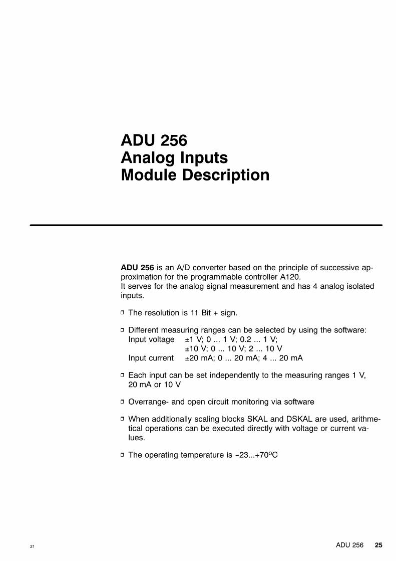
21 ADU 256 25
ADU 256Analog InputsModule Description
ADU 256 is an A/D converter based on the principle of successive ap-proximation for the programmable controller A120.It serves for the analog signal measurement and has 4 analog isolatedinputs.
The resolution is 11 Bit + sign.
Different measuring ranges can be selected by using the software:Input voltage ±1 V; 0 ... 1 V; 0.2 ... 1 V;
±10 V; 0 ... 10 V; 2 ... 10 VInput current ±20 mA; 0 ... 20 mA; 4 ... 20 mA
Each input can be set independently to the measuring ranges 1 V,20 mA or 10 V
Overrange- and open circuit monitoring via software
When additionally scaling blocks SKAL and DSKAL are used, arithme-tical operations can be executed directly with voltage or current va-lues.
The operating temperature is --23...+70oC

21ADU 25626
1
2
3
4
5
6
7
8
9
10
11
12
13
14
15
16
17
18
19
20
21
22
Figure 7 Front view and fill-in label of ADU 256
4 General
ADU 256 can be installed in any slot of the subracks DTA 200, 201 and 202.
4.1 Physical Characteristics
The standard size module has bus contact at the rear and periphery connection at thefront via screw/plug-in terminals.
One of the enclosed fill-in labels is inserted in the attachable cover of the subrack nearto the viewing window for the LED indicators. System relevant data (e.g. signal names)are to be entered in the fields provided.

21 ADU 256 27
4.2 Mode of Functioning
First of 4 Input Circuits
2120191817161514
109876543
12
1213
11
22
U
U
M
M
4
3
2
1
YE ”U”
+15 V
0 V
--15 V
--
--
MUX
0 V--15 V +15 V
PAB
Bit 11
.
.
.
.
.
.
.
.
.
.
Bit 0
80C31
REF
Param.
0 V--15 V +15 V Bit 12Bit 13Bit 14
A/D
YE ”ready”
TOTUSNPAB
PAB
PAB
5 V
seriell
Figure 8 Simplified Schematic for the ADU 256
5 Operating and Display Elements
The front side of the ADU contains the follwing indicators:
1 x yellow LED ”U” for the power supply 24 VON: Power supply is availableOFF: Power supply is not available
1 x yellow LED ”ready” for the processor operationON: Processor operation of the ADU and the ALU is without faultOFF: Fault in the processor operation

21ADU 25628
6 Configuration
The following should be configured:
I/O slot adresses (compare 3.1)Type of input and error evaluation (compare 6.2)Cabling (running of cables, shielding, (compare 6.3)Connection and assignment of signal addresses (compare 6.4)Connection representation of the periphery signals (DIN A3 forms, compare 6.5)
6.1 I/O Slot Adresses
I/O slot addresses (to be determined according to the chapter 3, ”Equipment and ...”).The module has no setting elements for addressing.The moduls must be entered via Dolog AKF as ”ADU 206” moduls instead of”ADU 256”.
6.2 Type of Input and Error Evaluation
6.2.1 Type of Input (Selection of the Measuring Range)The selection of the current input or voltage input is obtained through the type of con-nection. The setting of the corresponding measuring range is done with AKF softwarein the operand QBx.123).
In the initial stage QBx.1 = 0, that means:
All 4 inputs are set to measuring range +1 V or +20 mA +1 VNo monitoring for overrangeNo monitoring for open circuitBipolar operation
Following presettings are available for the ADU 206. These settings are obtained byadding the following values:
QBx.123) =1 (Bit 0) Measuring range +10 V on input 12 (Bit 1) Measuring range +10 V on input 24 (Bit 2) Measuring range +10 V on input 38 (Bit 3) Measuring range +10 V on input 416 (Bit 4) Unipolar mode, Resolution 12 Bit without sign, can also be used in
combination with open circuit monitoring, for outputs conversion ofdigital values is required.
32 (Bit 5) All 4 inputs to measuring range 0.2 ... 1 V ormeasuring range 4 ... 20 mA when jumpers are used on the inputswith simultaneous open circuit monitoring for currents <2.08 mA or
47 (Bit 5) all 4 inputs to measuring range 2 ... 10 V. No jumpers on the inputs.64 (Bit 6) Monitoring for measured values greater then nominal value + tolerance
(overload capability) on all 4 inputs.128 (Bit 7) Without significance, set value always 0.
23) x = Node number

21 ADU 256 29
Table 12 Possible QBx.124) Combinations
Con- Input 1 Input 2 Input 3 Input 4 Polarity Open- Overrange-tens of circuit- moni-QBx.124) monit. toring
1 +10 V +1 V / +20 mA +1 V / +20 mA +1 V / +20 mA Bipolar no no2 +1 V / +20 mA +10 V +1 V / +20 mA +1 V / +20 mA Bipolar no no3 +10 V +10 V +1 V / +20 mA +1 V / +20 mA Bipolar no no4 +1 V / +20 mA +1 V / +20 mA +10 V +1 V / +20 mA Bipolar no no5 +10 V +1 V / +20 mA +10 V +1 V / +20 mA Bipolar no no6 +1 V / +20 mA +10 V +10 V +1 V / +20 mA Bipolar no no7 +10 V +10 V +10 V +1 V / +20 mA Bipolar no no8 +1 V / +20 mA +1 V / +20 mA +1 V / +20 mA +10 V Bipolar no no9 +10 V +1 V / +20 mA +1 V / +20 mA +10 V Bipolar no no10 +1 V / +20 mA +10 V +1 V / +20 mA +10 V Bipolar no no11 +10 V +10 V +1 V / +20 mA +10 V Bipolar no no12 +1 V / +20 mA +1 V / +20 mA +10 V +10 V Bipolar no no13 +10 V +1 V / +20 mA +10 V +10 V Bipolar no no14 +1 V / +20 mA +10 V +10 V +10 V Bipolar no no15 +10 V +10 V +10 V +10 V Bipolar no no
16 0 ... 1 V / 0 ... 1 V / 0 ... 1 V / 0 ... 1 V /0 ... 20 mA 0 ... 20 mA 0 ... 20 mA 0 ... 20 mA Unipolar no no
31 0 ... 10 V 0 ... 10 V 0 ... 10 V 0 ... 10 V Unipolar no no3225) 0.2 ... 1 V / 0.2 ... 1 V / 0.2 ... 1 V / 0.2 ... 1 V /
4 ... 20 mA 4 ... 20 mA 4 ... 20 mA 4 ... 20 mA Bipolar yes no4725) 2 ... 10 V 2 ... 10 V 2 ... 10 V 2 ... 10 V Bipolar yes 26) no4827) 0.2 ... 1 V / 0.2 ... 1 V / 0.2 ... 1 V / 0.2 ... 1 V /
4 ... 20 mA 4 ... 20 mA 4 ... 20 mA 4 ... 20 mA Unipolar yes no6327) 2 ... 10 V 2 ... 10 V 2 ... 10 V 2 ... 10 V Unipolar yes 26) no
64 +1 V / +20 mA +1 V / +20 mA +1 V / +20 mA +1 V / +20 mA Bipolar no yes65 +10 V +1 V / +20 mA +1 V / +20 mA +1 V / +20 mA Bipolar no yes66 +1 V / +20 mA +10 V +1 V / +20 mA +1 V / +20 mA Bipolar no yes67 +10 V +10 V +1 V / +20 mA +1 V / +20 mA Bipolar no yes68 +1 V / +20 mA +1 V / +20 mA +10 V +1 V / +20 mA Bipolar no yes69 +10 V +1 V / +20 mA +10 V +1 V / +20 mA Bipolar no yes70 +1 V / +20 mA +10 V +10 V +1 V / +20 mA Bipolar no yes71 +10 V +10 V +10 V +1 V / +20 mA Bipolar no yes72 +1 V / +20 mA +1 V / +20 mA +1 V / +20 mA +10 V Bipolar no yes73 +10 V +1 V / +20 mA +1 V / +20 mA +10 V Bipolar no yes74 +1 V / +20 mA +10 V +1 V / +20 mA +10 V Bipolar no yes75 +10 V +10 V +1 V / +20 mA +10 V Bipolar no yes76 +1 V / +20 mA +1 V / +20 mA +10 V +10 V Bipolar no yes77 +10 V +1 V / +20 mA +10 V +10 V Bipolar no yes78 +1 V / +20 mA +10 V +10 V +10 V Bipolar no yes79 +10 V +10 V +10 V +10 V Bipolar no yes
80 0 ... 1 V / 0 ... 1 V / 0 ... 1 V / 0 ... 1 V /0 ... 20 mA 0 ... 20 mA 0 ... 20 mA 0 ... 20 mA Unipolar no yes
95 0 ... 10 V 0 ... 10 V 0 ... 10 V 0 ... 10 V Unipolar no yes9625) 0.2 ... 1 V / 0.2 ... 1 V / 0.2 ... 1 V / 0.2 ... 1 V /
4 ... 20 mA 4 ... 20 mA 4 ... 20 mA 4 ... 20 mA Bipolar yes yes11125) 2 ... 10 V 2 ... 10 V 2 ... 10 V 2 ... 10 V Bipolar yes 26) yes11227) 0.2 ... 1 V / 0.2 ... 1 V / 0.2 ... 1 V / 0.2 ... 1 V /
4 ... 20 mA 4 ... 20 mA 4 ... 20 mA 4 ... 20 mA Unipolar yes yes12727) 2 ... 10 V 2 ... 10 V 2 ... 10 V 2 ... 10 V Unipolar yes 26) yes
24) x = Node number25) A valid measured value should be applied to the unused inputs. This can be achieved by using a reference
measuring point or by voltage input (parallel circuit) or by current input (series circuit) to the inputs.26) Monitoring for voltages <2 V.27) Can be used for manufacturing index 274 905.13 (firmware 277 707.01) upwards.

21ADU 25630
Note After switching on the first measured value corresponds to the initial state of thetype of input. A change in the type of input influences the measured value at the ear-liest after the second cycle. As for ADU 206 a conversion cycle takes 10 ms, it canhappen even later in case of scan time less than 10 ms.
Note In unipolar operation a conversion of the digital values is required for outputs(see also Table 15, page 35).The program for the conversion can be e.g. as follows:
:LD IWx.1:SHR V1:= MW1
6.2.2 Linking into the User ProgramThe loading of the operand QBx.124) should not be done for each program cycle (unne-cessary extension of the processing time).Therefore, while loading use the switch-on marker in combination with a jump operande.g. :
:A SM2:JF =Y1:LD V32:= QB2.1
Y1 :***

21 ADU 256 31
6.2.3 Error EvaluationSystem marker SMx.1 28) sends a group signal when there is an error on the ADU 256.Detailed error data can then be scanned in the operand IBx.1 28).
Table 13 Possible IBx.128) scanning combinations
IBx.128) ADU UB 2...10 V / Uni- Overrange or open circuitdoesn’t missing 4...20 mA on polar when current <2.08 mA on
binary decimal work * Input 1...4 Inp. 4 Inp. 3 Inp. 2 Inp. 1Bit 7 Bit 6 Bit 5 Bit 4 Bit 3 Bit 2 Bit1 Bit 0
0001 0000 16 0 0 0 1 0 0 0 00010 0000 32 0 0 1 0 0 0 0 01000 0000 --128 1 0 0 0 0 0 0 01000 0001 --127 1 0 0 0 0 0 0 11000 0010 --126 1 0 0 0 0 0 1 01000 0011 --125 1 0 0 0 0 0 1 11000 0100 --124 1 0 0 0 0 1 0 01000 0101 --123 1 0 0 0 0 1 0 11000 0110 --122 1 0 0 0 0 1 1 01000 0111 --121 1 0 0 0 0 1 1 11000 1000 --120 1 0 0 0 1 0 0 01000 1001 --119 1 0 0 0 1 0 0 11000 1010 --118 1 0 0 0 1 0 1 01000 1011 --117 1 0 0 0 1 0 1 11000 1100 --116 1 0 0 0 1 1 0 01000 1101 --115 1 0 0 0 1 1 0 11000 1110 --114 1 0 0 0 1 1 1 01000 1111 --113 1 0 0 0 1 1 1 11010 1111 --81 1 0 1 0 1 1 1 11100 0000 --64 1 1 0 0 0 0 0 0
* Cause: Overrange or open circuit on each of four inputs orProcessor monitoring active orUB = 24 V missingADU is initializing.
Values 16 and 32 are reflects of the default input option. They are not errors.
6.3 Cabling
Note For general cabling and installation guidelines see user manual, chapter 5.2”EMC Measures”.
For the connection shielded cables (2 x or 4 x 0.5 mm2, twisted per channel) shouldbe used. All channels can be placed in a common shielded cable.
The shield should be connected to ground at one side with short cable (<20 cm).For higher noise levels, the cable shield should be on both sides. See also user ma-nual chapter 5.2 ”EMC Measures”.
The cable should not be laid together with power supply lines or other similarsources of electrical disturbances. Distance >0.5 m.
28) x = Node number

21ADU 25632
6.4 Connection and Assignment of Signal Addresses
20
19
18
17
16
15
14
10
9
8
7
6
5
4
3
1
2
12
13
11
22
U
UBM2
U
0.16 A
--
+
+
--
IIWx.1 --
+
IIWx.3 --
+
IWx.2
IWx.4
I --
+
I --
+
21
20
19
17
16
15
10
9
8
7
6
5
4
3
U --
+
U --
+
*
*
*
*
* For current inputs please usethe enclosed jumpers.
Figure 9 Connection Example of ADU 256
The following can be connected:2 pole voltage sensors ±1 V; 0 ... 1 V; 0.2 ... 1 V;
±10 V; 0 ... 10 V; 2 ... 10 V or2 pole current sensors ±20 mA; 0 ... 20 mA; 4 ... 20 mAThe selection of current (I) or voltage (U) input is obtained depending on the connec-tion (mixed operation permissible)For connection of current sensors following jumpers are required:Jumper 3-4 for IWx.1
7-8 for IWx.214-15 for IWx.318-19 for IWx.4.
The ADU is delivered with the jumpers installed.
Unused voltage inputs should be connected as follows:Jumper 3-4 or 4-6 for IWx.1
7-8 or 8-10 for IWx.214-15 or 15-17 for IWx.318-19 or 19-21 for IWx.4.

21 ADU 256 33
For the measurung ranges ±1 V / ±10 V / ±20 mA each input can be usedindependently as required. The measuring ranges 2 ... 10 V / 4 ... 20 mA are alwaysfor all 4 inputs. In this case a valid measured value should be applied to the unused in-puts.
The analog input values are transferred after conversion to the input wordsIWx.1 ... IWx.4.
Corresponding signal names or signal addresses should be entered in the fill-in labels.
6.4.1 Grounding of the ShieldsLay the shielded cables over the cable earthing bar CER 001
At the level of the corresponding cable cleat remove the shield insulation
Press the cable with the opened shield in the cable cleat (contact to hat rail)
With cable clip relieve each cable from traction as shown in Figure 10
cable earthing bar CER 001, AEG E-No 424 244 739
Figure 10 Grounding of the Shields
6.5 Documentation Aids
For project specific system documentation and representation of the connected processperiphery A3 forms are provided.
These forms are for:
conventional processing and are part of the A120 form block (see ordering details)
Ruplan processing (TVN version) and are part of the A120 data base

21ADU 25634
4 Specifications
4.1 AllocationProgrammable Controllers A120Structure In I/O structure
4.2 Power SupplyExternal Power Supply UB = 24 VDC, typ. 70 mA, max. 100 mAInternal via I/O bus 5 VDC; typ. 60 mA, max. 100 mA
4.3 InputsNo. of Inputs 4, (2 pole as voltage or current inputs)Isolation Optical coupler, from internal system bus and
24 V supply,Varistor (voltage dependent protective resistor) to PE(protective earth),Inputs not isolated from each other.
Linear Measuring Range ±1 V / ±20 mA (depending on the connection)0.2 ... 1 V / 4 ... 20 mA (depending on the connection)0 ... 1 V / 0 ... 20 mA (depending on the connection)±10 V / 0 ... 10 V /2 ... 10 V (depending on the QBx.1)
Table 14 Conversion Values of ADU 256 on bipolar mode
Analog value Decimal value CommentsVoltage inputs (V) Current inputs (mA)+1 V +10 V 2 ... 10 V +20 mA 4 ... 20 mA
--1.024 ... --10.24 --20.48 ... --32 768 ... Overrange--1.001 --10.01 ... --20.02 --32 016
--1.00 --10.00 --20.00 --32 000--0.50 --5.00 --10.00 --16 000--0.10 --1.00 --2.00 --3 200--0.05 --0.50 --1.00 --1 600--0.01 --0.10 --0.20 --320--0.001 --0.01 --0.02 --32--0.0005 --0.005 --0.01 --160.00 0.00 +2.00 0.00 +4.00 0+0.0005 +0.005 +2.004 +0.01 +4.008 +16+0.001 +0.01 +2.008 +0.02 +4.016 +32+0.01 +0.10 +2.08 +0.20 +4.16 +320+0.05 +0.50 +2.40 +1.00 +4.80 +1 600+0.10 +1.00 +2.80 +2.00 +5.60 +3 200+0.50 +5.00 +6.00 +10.00 +12.00 +16 000+1.00 +10.00 +10.00 +20.00 +20.00 +32 000
+1.001 ... +10.01 ... +10.01 ... +20.02 ... +20.02 ... +32 016 ... overrange+1.024 +10.24 +10.19 +20.47 +20.38 +32 752
linearrange

21 ADU 256 35
Table 15 Conversion values of ADU 256 on unipolar mode
Analog-values Hexa-De- Decimal-valuesVoltage inputs (V) Current inputs (mA) cimal-values0 ...1 V 0 ...10 V 0.2 ...1 V 2 ...10 V 0 ... 20 mA 4 ... 20 mA HEX DEZ
0 0 0.2 2 0 4 0 00.1 1 2 1900 6 4000.5 5 10 7D00 32 0000.6 6 12 95F0 --27 136* (38 384)1 10 1 10 20 20 FA00 --1 536* (64 000)
* displayed on programming panel
Common mode voltage onreturn conductors betweeneach other for 10 V, upper range value max. ±2 V
for 1 V, upper range value max. ±11 V
Max. Voltage onVoltage Inputs ±30 V for inputs between each other for 1 min.Max. Current onCurrent Inputs 40 mA continuousInput Resistance 50 Ω for current inputs
>1 MΩ for voltage inputs
Insulation Voltage Max. 500 V, Process connection against internal I/O busmax. 500 V, Process connection against externalpower supply 24 V
Common Mode Suppressionagainst ground Min. 60 dB for 1 kHz
Filter time constant of theinputs 1.5 ms
4.4 ConverterConversion Time Max. 10 ms for all 4 inputsResolution of the converter 11 Bit + sign (bipolar) or 12 Bit (unipolar)Operation Error Limit Max. 0.4 % (0 . . . 60 oC) with respect to the used
voltage rangemax. 0.56 % (0 . . . 60 oC) with respect to theused current range
4.5 Processor, MemoryProcessor Type Microprocessor Intel 80C31 (8 Bit)Memory 128 Byte RAM for data exchange
32 kByte EPROM for firmware
4.6 Data InterfaceInternal I/O Bus Parallel I/O bus, see User Manual, chapter 4
”Specifications”

21ADU 25636
4.7 Error EvaluationIndicators see chapter 5, page 27A120 System Marker (for 1 signal)SM 31 ... SM 48 I/O node number on slot 1 ... 18 is absentSMx.1 group signal when there is an errorIBx.1 For detailed error data see chapter 6.2.3, page 31
4.8 Physical CharacteristicsModule Standard size boxFormat 3 HE, 8 TWeight 330 g
4.9 Type of ConnectionProcess 2 pluggable 11 pole screw/plug-in terminalsCable to Process Minimum crosssection 0.5 mm2, twisted pairwise
reference conductor in cable, shielded e.g.JE-LiYCY 2 x 2 x 0.5
Distance to potential >0.5 m to disturbance sourcesCable length max. 100 m, longer cables on request
I/O bus (internal) rearside connector 1/3 C30M
4.10 Environmental CharacteristicsStandards VDE 0160, UL 508System Data See User Manual chapter 4 “Specification”Temperature in Operation --25 ... +70 oC constant
--30 ... +85 oC short--time (10 minutes)Power Dissipation 2 W typical, max. 3 W
4.11 Ordering DetailsModule ADU 256 424 701 248Cable to Process JE-LiYCY 424 234 035DIN A3 Form Block,Process-Peripherals A91M.12-271 683
Replacement Fill-in Label 424 701 662
Subject to technical modifications!

21 ALU 252 37
ALU 252Central Processing UnitModule Description
The CPU ALU 252 together with the power supply DNP 255 and theDTA 200 form the basic unit of the A120 programmable controller.
This module provides the following features:
a central processing unit (CPU)
a memory for basic software, user program and processor signals
an RS 232C port for the programming panel
RS 485 port for Modnet 1/SFB (only slave).
The operating temperature is --25 ... +70oC

21ALU 25238
card
battery 2
battery 1
run
ready
software
Figure 11 Front View and Fill-In Labels of ALU 252
1 General
The module ALU 252 contains the processor (CPU) of the A120 with an integratedcommunication port for the Modnet 1/SFB, via which it can be connected as a slave toa superior controller (master).Together with the power supply DNP, the ALU generates an internal I/O bus (modifiedPAB1). The ALU 252 can only be inserted in slot 0 (left of the power supply) in thebackplane DTA 200.
1.1 Physical Characteristics
The module consists of 3 PCBs which are assembled in a 2-slot size module with 16Tconstruction width and 3HE construction height. They are connected using ribbon cableand bus planes. The essential components of the modules are:
Micro-processor32 KB EPROM for basic software32 KB RAM for signal memory and system variables64 KB RAM for user program and organization data (approx. 12 k instructions)Real time clock with date functions and calendar functionsFront slot for EPROM card (PC 001)Battery compartments for 2 back-up batteriesDIP switch for starting mode and start behaviorFront port for programming panel (RS 232C)3 rear ports for I/O bus (modified PAB1)

21 ALU 252 39
DIP switch for slave address and transmission rateFront port for Modnet 1/SFB networking (RS 485)
Note PC 001 card should be used omly for the start--up operation (no continuousoperation).
1.2 Functions
The processor provides the following features:
Generation of an internal processing clock pulseOrganization of internal data traffic on the I/O bus between all modulesWriting the process input signals into the signal memoryProcessing of the user programStoring intermediate results (markers) in the signal memoryOutput of the process output signals from the signal memoryControlling of real time clockOperation of the serial ports for program transmissionsMonitoring of : processor run,
batteries,power supply voltage,program cycle
Sending and receiving data telegrammes via Modnet 1/SFB
2 Operating and Display Elements
The module provides the following operation and indicators elements:
yellow LED ”ready”on: power supply voltage available and processor is runningoff: power supply voltage is not available or the processor is not
running
yellow LED ”run”on: user program is runningblinks with 3 puls./s: fault during loading of the user program from the PC 001blinks with 5 puls./s: ALU in EPROM operation and PC 001 is not available or
no program on the PC 001blinks with 7 puls./s: only for ALU 201, basic software on the PC 001 and
simultaneosly in EPROM of the ALUoff: user program is not running
red LED ”battery 1”on: battery 1 has low voltage or is missingoff: battery 1 voltage is in the setpoint range
red LED ”battery 2”on: battery 2 has low voltage or is missingoff: battery 2 voltage is in the setpoint range

21ALU 25240
3 Configuration
Now you have to configure the following features:
Type of ALU (compare 3.1)Start-up characteristics (compare 3.2)Operating mode (compare 3.3)Operation of the ALU as Slave (compare 3.5)Second back-up battery (compare 3.6)
3.1 Type of ALU
You have to enter the type of ALU in the menu ”Setup” via Dolog AKF software.
3.2 Set Start-up Characteristics (B0 and B1 DIP Switches)
The start-up characteristic is set at the operating mode switch using B0 and B1. Fourtypes of starting modes are possible:
Cold Restart The programmable controller starts using a initialized signal memory at the beginning ofthe program.
Hot Restart The programmable controller continues the program in principle at the interrupted posi-tion using the saved signal memory data.
Manual Start The programmable controller remains in a halt position when power supply is switchedon. The programmable controller has to be started manually via a programming panel.
Automatic Start The programmable controller starts automatically when the power supply voltage isswitched on.
B0
B1
B2
B3
B0
B1
B2
B3
ON OFF
Cold Restart * Hot Restart
ON OFF
B0
B1
B2
B3
B0
B1
B2
B3
ON OFF
Manual Start * Automatic Start
ON OFF
* As Delivered
Figure 12 Set Start-Up Characteristics at the B0 and B1 DIP Switches

21 ALU 252 41
Caution during hot restart:1. In case of EPROM operation with PC 001, the PC automatically starts with
a cold restart. Hot restart after a manual stop of the PC is possible via theprogamming panel.
2. On switching off, it is necessary that the power supply circuits for thesensors (inputs) has a longer backup time than 5V bus power supply (seealso chapter ”Connection Diagram of the UB Supply” of the user manual.
3.3 Setting the Operating Mode (B2 DIP Switch)
The user program is programmed off-line on the programming panel and can optionallybe loaded
via the EPROM card PC 001 into the RAM of the ALU. If you take this choise, theEPROM card has to be recorded previously using the EPROM programming stationEPS 2000 (EPROM operation).from the programming panel into the RAM of the ALU (RAM operation)
You have to set the operating mode at the operating mode switch using B2.
B0
B1
B2
B3
B0
B1
B2
B3
ON OFF
RAM Operation * EPROM Operation
ON OFF
* As Delivered
Figure 13 Setting the Mode Selector at the B2 DIP Switch
Caution Insert PC 001 only in ALU if disconnected from supply
3.4 Real Time Clock
The in-built real time clock controls the following parameters:
Time: Seconds, minutes and hoursCalendar: Days of the week, the day’s date, month and year. Leap-years are
corrected automatically.
You can set the clock in the software using the programming panel (AKF funktion).No settings are necessary as far as the hardware is concerned.The clock is backed up via the battery of the ALU 252, and therefore continues runningif the power supply voltage is switched off.

21ALU 25242
3.5 Operation of the ALU as Slave
The ALU 252 can be linked to a master as slave via a RS 485 port (e.g. to the BIK 151in a A350 and/or A500, compare Figure 14). In this case you have to take the followingsteps:
Set the transmission rate (compare 3.5.1)Set the slave address (compare 3.5.2)Prepare a bus cable (see user manual chapter 3.7 ”Configuration the SystemFieldBus”)
Note If the ALU is not used in networking mode, the DIP switches B3 andA0 ... A7 which are provided for the setting of transmission rates are unimportant.
Apart from the A120, other programmable controllers (e.g. A350, A500) or I/O nodessuch as DEA-H1/DEA-K1, DEA 105/DEA 106 can also be linked to the master. Themax. number of linkable slaves is 28 slaves per BIK module. 16 is the maximum num-ber of I/O nodes.
Slave Slave Slave
Master
max. 3 BIK-Modulesfor 1N-Procedures
Figure 14 Beispiel einer Kopplung zwischen A500 (Master) und mehreren A120 (Slaves)

21 ALU 252 43
3.5.1 Setting the Transmission Rates for RS 485 (Modnet 1/SFB)Self-Clocked mode is used for data transmission. Two different transmission rates areavailable depending on the cable length:
Table 16 Dependence of the Transmission Rate on the Length of Cable
Transmission Rate max. Cable Length
62.5kBd 1200 m375kBd 300 m
In order to guarantee a correct data transfer, the cable lengths which are specified inTable 16 must not be exceeded.
The transmission rate is set using the DIP switch B3 on the front of the ALU (compareFigure 15).
B0
B1
B2
B3
B0
B1
B2
B3
ON OFF
62.5 kBd * 375 kBd
ON OFF
* As Delivered
Figure 15 Setting the Transmission Rate at the B3 DIP Switch
Note Ensure that the same transmission rate is set on all network nodes of a bus line(master with its slaves). Furthermore, the network nodes which permit a choice be-tween self-clocked-mode and synchronous mode should be set to the self-clocked-mode. For more information see the corresponding module descriptions.

21ALU 25244
3.5.2 Setting the Slave Address on the ALUThe slave address is set using the DIP switch A0 ... A7 (upper DIP switch field on thefront of the module).A number between 1 and 126 is allowed as an address. The address has to be duallycoded first, before the switch position is determined. The position of the switches is de-termined by the coefficients of the two’s power. A0 is the lowest value bit and A7 hasthe maximum value bit.Figure 16 shows as an example the switch position for the address 52. Other address-es are listed in Table 17.
Address 52 Switch Position DIP SwitchCode Dually Read A0 ... A7 Set A0 ... A7
ON OFF
0 * 20 = 0 A0 = 0 A0
0 * 21 = 0 A1 = 0
1 * 22 = 4 A2 = 1
0 * 23 = 0 A3 = 0
1 * 24 = 16 A4 = 1
1 * 25 = 32 A5 = 1
0 * 26 = 0 A6 = 0
+ 0 * 27 = 0 A7 = 0 A7
= 52
1 2 3
0→ OFF
1→ ON
Figure 16 Addressing Example for Slave Address 52
Table 17 Setting of the Slave Address on the DIP Switch Field A (Switch A0 ... A7)
Switch Address029) 1 2 3 4 5 6 7 8 9 10 11 12 13 14 15 16
A0 OFF ON OFF ON OFF ON OFF ON OFF ON OFF ON OFF ON OFF ON OFFA1 OFF OFF ON ON OFF OFF ON ON OFF OFF ON ON OFF OFF ON ON OFFA2 OFF OFF OFF OFF ON ON ON ON OFF OFF OFF OFF ON ON ON ON OFFA3 OFF OFF OFF OFF OFF OFF OFF OFF ON ON ON ON ON ON ON ON OFFA4 OFF OFF OFF OFF OFF OFF OFF OFF OFF OFF OFF OFF OFF OFF OFF OFF ONA5 OFF OFF OFF OFF OFF OFF OFF OFF OFF OFF OFF OFF OFF OFF OFF OFF OFFA6 OFF OFF OFF OFF OFF OFF OFF OFF OFF OFF OFF OFF OFF OFF OFF OFF OFFA7 OFF OFF OFF OFF OFF OFF OFF OFF OFF OFF OFF OFF OFF OFF OFF OFF OFF
Switch Address17 18 19 20 21 22 23 24 25 26 27 28 ... 123 124 125 126
A0 ON OFF ON OFF ON OFF ON OFF ON OFF ON OFF ... ON OFF ON OFFA1 OFF ON ON OFF OFF ON ON OFF OFF ON ON OFF ... ON OFF OFF ONA2 OFF OFF OFF ON ON ON ON OFF OFF OFF OFF ON ... OFF ON ON ONA3 OFF OFF OFF OFF OFF OFF OFF ON ON ON ON ON ... ON ON ON ONA4 ON ON ON ON ON ON ON ON ON ON ON ON ... ON ON ON ONA5 OFF OFF OFF OFF OFF OFF OFF OFF OFF OFF OFF OFF ... ON ON ON ONA6 OFF OFF OFF OFF OFF OFF OFF OFF OFF OFF OFF OFF ... ON ON ON ONA7 OFF OFF OFF OFF OFF OFF OFF OFF OFF OFF OFF OFF ... OFF OFF OFF OFF
29) As Delivered

21 ALU 252 45
3.6 Back-up Batteries
A battery is included in the ALU but shall not be used before the initial start-up so thatit can be conserved. It supplies the clock, the RAM of the signal memory and the RAMfor the user-programmed logic. One can achieve a larger back-up reserve by mountinga second battery (see accessories).
The battery back-up switching is designed in such a manner that battery 1 supplies theback-up current until it has been used up. After this, battery 2 takes over the rest of theback-up without interruption. A used battery can also be replaced in this manner if thepower voltage is interrupted - as long as the other one still functions.
If there is no voltage or only under voltage in one of the batteries, the red LED ”bat 1”and/or ”bat 2” is displayed. See “Specifications” for the life time of the batteries.
Note Changing the batteries simultaneously can only be carried out without data lossif the power supply voltage is connected.
Caution1. Due to voltage peaks do not touch the battery contacts of the ALU2. Used batteries are special refuse. Please only dispose of them in
the waste disposal containers provided.

21ALU 25246
3.7 Connection
PC 001Slave-Address
Operating Mode
YDL 052
Programming Panel
RS 232C
Networking via SystemFieldBus
Master
RS 485
Option
Battery
ALU EPROM-Card
PC 001
Figure 17 Connection

21 ALU 252 47
3.8 Connector Pin Assignment
3.8.1 RS 232C port
Pin Signal Meaning
2 D2 Received Data3 D1 Transmitted Data5 E2 Signal Ground
Connector Pin AssignedConnector Pin not Assigned
Figure 18 Pin Assignment of the RS 232C Port
For the connection of the ALU to the programming panel following 3 m cables can beused:
YDL 048 for programming panel with 25 pole RS 232C portYDL 052 for programming panel with 9 pole RS 232C port
For terminal assignment with cable extensions please refer to the user manual ”Kabelfür die Produktfamilie Modicon A...”. Document part number A91M.12-271 975.
3.8.2 RS 485 Port
Pin Signal Meaning
3 DATAN Data Signal negated5 RGND Protective Ground, Shield (R-Ground)8 DATA Data Signal
Connector Pin AssignedConnector Pin not Assigned
Figure 19 Pin Assignment of the RS 485 Port

21ALU 25248
3.9 Documentation Aids
For the project specific system documentation e.g. start-up characteristics, operatingmode etc. DIN A3 forms are provided.These forms are for:
conventional processing and are part of the A120 form block (see ordering details)Ruplan processing (TVN version) and are part of the A120 data base
3.10 Creating and Transmitting Programs at Initial Start-up
Note The following items can also be found in the user manual Dolog AKF → A120 /A250 in the chapter ”Programming”.
Dolog AKF12: Create user programm in off-line mode (see Dolog AKF12-Softwarepart ”Programming”)
Dolog AKF12: Transfer program to programmable controller RAM and test itConnect programming panelSwitch on programmable controller (power on). Insert battery 1 in upper compart-ment (+ in upward position), note dateUse ”Load”, ”Set Date/Time” to enter the current dataLink programm under ”Load”, ”Program Link” (see AKF chapter ”Program Link”)Transfer program to RAM with ”Load”, ”Program to PC” (see AKF chapter ”Pro-gram to PC”)Start programmable controller with ”Online”, ”Start PC” (see AKF chapter ”StartPC”)During cyclic processing of the user program the yellow function display ”run” ison at the ALUTest the program with ”Online”, ”Dyn. Status Display” resp. ”Online”, ”Online-List”(see AKF chapter ”Online”)Eliminate the faults when present. The notes mentioned under ”Error Evaluation”can be a help for this purpose. These are given in the ”Specifications” of the cor-responding module (I/O module)Possibly determine hardware status with ”Online”, ”PC-Status” (see AKF chapter”PC-Status”)If you want to change anything after the test, you can edit the program offline.Then the changed program part will be transferred to the running or not runningprogrammable controller with ”Load”, ”Exchange Online”. Then the program has tobe tested again (see AKF chapter ”Exchange Online”).
During this procedure the A120 with ALU 202 is running.

21 ALU 252 49
4 Specifications
4.1 AllocationDevice A120Structure Slot 0 in the primary backplane DTA 200
4.2 Power PortInternal (I/O bus) +5 V, typical 500 mA, max. 800 mAInternal (RS 232 C) ±12 V according to DIN 66020
4.3 Data PortI/O Bus Internal, parallel I/O bus. For further details please refer
to ”Specifications” in user manualRS 232C (V.24) serial port according to DIN 66 020, potentially linked
Pin Assignment see Figure 18, page 47Transmission Rate 9.6 kbaudData Format see ”Specifications” in user manual
Modnet 1/SFB according to RS-485 (symmetrically-serial), floatingPin Assignment see Figure 19, page 47Transmission Rate 62.5 kbaud at max. 1200 m
375 kbaud at max. 300 mData Format see ”Specifications” in user manual
4.4 Type of ProcessorIntel 8344 Micro-processor (8 Bit) at ALU 252
4.5 Memory CapacityRAM 32 KB for signal memory and system variables
64 KB (approx 12 k logical instructions) for user program32 KB for basic software at ALU 202L
EPROM 32 kB for basic software at ALU 202EPROM Card PC 001 128 kB in order to archive the user program
(32 kB of these are reserved for basic software)
4.6 ClockFrequence Stability ±100 ppm30)
4.7 Back-up BatterySize 1/2 AAPlaced on the I/O Bus in order to back up ALU RAM, clockVoltage (No-Load Operation) 3.6 VCapacity 0.85 Ah
Life TimeNo-Load Operation (NotConnected) 10 yearsConserved Operation 3 years typical, at least 4 months
30) ppm→ parts per million, 10 -6

21ALU 25250
4.8 LEDsyellow LED (above) readyyellow LED (below) runred LED (above) Battery error for battery 1red LED (below) Battery error for battery 2
4.9 Mechanical StructureModule in the 2-slot size moduleFormat 3 HE, 16 TWeight 500 g
4.10 Type of ConnectionI/O Bus 2 multipoint connectors 1/3 C30M,1 female multipoint
connector 1/3 R30FRS 232C 9 pole female multipoint connectorModnet 1/SFB 9 pole multipoint connector (for BBS1)
4.11 Environmental ConditionsStandards VDE 0160System Data See ”Specifications” in user manualPermissible AmbiantTemperature in Operation --25 ... +70 oC constant
--30 ... +85 oC short--time (10 minutes)Power Dissipation 2.5 W typical, max. 4 W
4.12 Ordering DetailsModule ALU 252 424 274 957EPROM Card PC 001 424 075 263RS 485 Connector BBS 1 424 233 854Cable JE-LiYCY 424 234 035Connection Cable YDL 52 424 244 878Connection Cable YDL 48 424 270 552DIN A3 Form Block,Central Device Modules A91M.12-279 382
ReplacementsBatteries 424 249 065Fill-In Label 1 424 277 905Fill-In Label 2 (ALU 252) 424 274 982Basic Software on EPROMfor ALU 252 (BSW 126) 424 277 765Plastic Pull Handle (TBP 000) 424 235 247
Data is subject to technical alterations!

20 DAP 250, DAP 258 51
DAP 250, DAP 258Discrete Inputs and OutputsModule Description
The DAP 250 is an output module with 8 discrete, isolated inputs 24VDC and 8 discrete, isolated, semiconductor outputs 24 VDC, 2 A withshort circuit and overload protection.The operating temperature is --25 ... +70 oC
The DAP 258 is a 8 point, discrete relay output module.The operating temperature is --25 ... +70 oC

20DAP 250, DAP 25852
1
2
3
4
5
6
7
8
9
10
11
12
13
14
15
16
17
18
19
20
21
22
12345678910
11
12131415161718192021
22
Figure 20 Front view and fill-in label of DAP 250 and DAP 258
1 General
The Module can be installed in any slot of the subracks DTA 200, DTA 201 undDTA 202.
The operating voltage UB = 24 VDC for sensor supply (inputs) and of the relay coilsand the working voltage US = 24 VDC for the outputs should be supplied externally.The 5 V voltage supply is obtained internally via the I/O bus.
1.1 Physical Characteristics
The standard box type module has bus contact at the rear and periphery connectionvia screw/plug-in terminals at the front.
One of the enclosed fill-in labels is inserted in the attachable cover of the subrack nearto the viewing window for the LED displays. System relevant data (e.g. signal names)are to be entered in the fields provided.

20 DAP 250, DAP 258 53
1.2 Mode of Functioning
2120191817161514
109876543
12
1213
11
22
Q!
.
.
.
Q8
.
.
.
PAB
PAB
PAB
U
U
.
I1
.
.
.
.
M
.I8M
YE
RD
YE RD
YE
First of 8 Output Circuits
First of 8 Input Circuits
I>
Figure 21 Simplified Schematic for the DAP 250
2120191817161514
109876543
12
1213
11
22
PAB
U
U
M
Q8
M
First of 8 Output Circuits
RD
Q7
Q6
Q5
Q4
Q3
Q2
Q1
YE
47Ω
15 nF
Figure 22 Simplified Schematic for the DAP 258

20DAP 250, DAP 25854
2 Operating and Display Elements
The front side of the module contains 19 indicators (from upper end):
DAP 2501 x yellow LED ”U” for the working voltage of the 8 outputson: Working voltage is availableoff: Working voltage is not available1 x yellow LED ”I>” for overload or short circuit on the outputson: Short circuit or Overloadoff: Operation without fault8 x red LED ”1 ... 8” for the output signalson: Output has ”1” signaloff: Output has ”0” signal1 x yellow LED ”U” for external sensor supplyon: Sensor supply is availableoff: Sensor supply is not available8 x red LED ”1 ... 8” for input signalson: Input has ”1” signaloff: Input has ”0” signal or not connected
Cause- Sensor supply is not available- Reference potential M1 is cut
DAP 2581 x yellow LED ”U” for the supply of the relay coilson: Power supply voltage availableoff: Power supply voltage not available
8 x red ”1 ... 8” for the output signalson: Outputs lead to ”1” signaloff: Outputs lead to ”0” signal
For simulation purpose the simulator SIM 011 can be installed on the 8 inputs (lower 11pole screw/plug-in terminal).
3 Configuration
The following should be configured:
I/O slot addresses (compare 3.1)
Assignment of signal addresses to periphery signals and connection (compare 3.2)
Checking of the rated load, short circuit behaviou (compare 3.3)
Connection representation of the periphery signals (DIN A3 forms, compare 3.4)

20 DAP 250, DAP 258 55
3.1 I/O Slot Addresses
I/O slot addresses (to be determined according to the chapter 3, ”Equipment and ...”).The module has no setting elements for addressing.The moduls must be entered via Dolog AKF as ”DAP 220” moduls instead of”DAP 250”.The moduls must be entered via Dolog AKF as ”DAP 208” moduls instead of”DAP 258”.
3.2 Connection and Assignment of Signal Addresses
DAP 250
21
20
19
18
17
16
15
14
10
9
8
7
6
5
4
3
UB = 24 VDCM1
1
2
12
13
11
22
10A
Q1
Q8
.............
I1
I8
.............
US = 24 VDCM4
0.16
A
Figure 23 Connection Example for DAP 250
For inductive loads on the outputs use free wheeling diode directly parallel to the induc-tivity. This protective circuit is absolutely necessary, when in output lines switchingcontacts are present or when the wires to the periphery are very long.
Enter the corresponding signal names or addresses in the fill-in labels.

20DAP 250, DAP 25856
DAP 258
2120191817161514
109876543
UB = 24 VDCM2
12
1213
11
22
US = 24 ... 110 VDC / L = 24 ... 230 VACM4/N
0.16A
Q1
Q2
Q3
Q4
4A
4A
Q5
Q6
Q7
Q8
4A
4A
Figure 24 Connection Example for DAP 258
Each signal name resp. signal address should be entered in the fill-in lable.
If you connect inductive loads, you have to provide a protective circuit directly and par-allel to inductivity (operating coil):
for working voltages L = 230 VAC an additional, sufficiently provided (acc. to manu-facturer) RC circuit, necessary for increased service life and EMC immunityfor working voltages Us = 24 VDC a clamping diode (suppressor diode) for increasedservice life
Note For general cabling and installation guidelines see user manual, chapter 5.2”EMC Measures”.

20 DAP 250, DAP 258 57
3.3 Testing the Permissible Load, Short Circuit Behaviour
The load current for all outputs must correspond to the specifications.Protection measures and power supply connections should be carried out as given inuser manual chapter 3.3 ”Layout of Power Supply”.
Short Circuit Behaviour of DAP 250The output stages do not store overload information. When in case of overload theworking voltage is not switched-off the system tries to switch-on at the output stagesrepeatedly. This causes an increase in the component temperature.
Therefore the systemmarker SMx.1 assigned to the slot of DAP 250 should be linked inthe user program in such a way that in case of overload the outputs are switched overto 0 signal. This system marker switches to 1 signal when:
The working voltage US is not available
There is an occurence of short circuit or overload
The 10 A safety fuse is blown
3.4 Documentation Aids
For project specific system documentation and representation of the connected processperiphery A3 forms are available.
These forms are for:
conventional processing and are part of the A120 form block (see ordering details)
Ruplan processing (TVN version) and are part of the A120 data base

20DAP 250, DAP 25858
4 Specifications
4.1 AllocationProgrammable Controllers A120Structure In I/O structure
4.2 Power Supply DAP 250External Sensor Voltage UB = 24 VDCInternal 5 V; typ. 35 mA, max. 60 mA via I/O bus
Power Supply DAP 258External Sensor Voltage UB = 24 VDCInternal 5 V; typ. 35 mA, max. 60 mA via I/O bus
4.3 Process Interface DAP 250
InputsSensor Power Supply UB = 20 ... 30 V for all 8 inputsReference Potential M M1 for all 8 inputsNo. of Inputs 8Type of networking Optical coupler, isolated against I/O bus and against out-
putsSignal Rated Value +24 VSignal Level 1 signal +12 ... +30 V
0 signal --2 ... +5 VInput Current 7 mA for 24 V
8.5 mA for 30 VInput Delay 4 ms
OutputsWorking Voltage U Us = 20 ... 30 VDC, for all 8 outputsReference Potential M M4 for all 8 outputsNumber 8 semiconductor outputs
Construction with short circuit and overload protection,without restart inhibit,group display for overload/short circuit,group signal via system marker S11x.1
Type of Networking Potential-free (Optical coupler)
Load Connection Between output and reference potential M4
Logic Positive logicSignal Output Level 1 signal U = US -- 0.4 V;
0 signal 0 ... +2 V, <1 mALimiting of the inductive switch-off voltage at --15 V(built in fast de-energization)
Load Current for eachOutput 10 mA ... 2 A, max. 10 W at bulbsSwitch-on Current forBulbs Ion = 10 x INLoad Current for all

20 DAP 250, DAP 258 59
Outputs max. 8 A
Required External Fuse 10 A, fast
Operating Delay <1 ms
Protective Circuit for Free wheeling diode directly parallel to the inductivity In-ductive Loads absolutely necessary, when in outputlines switching contacts are present or when the wires tothe periphery are very long or when the load current is>1 A
Switching Cycles 1000 /h (0.28 /s) for inductive load and max allowablecurrent for each output100 /s for ohmic load10 /s at max. bulb load
4.4 Process Interface DAP 258
Relay OutputsNumber 8 Normally open contacts (with LEDs)Type of Networking Contacts isolatedOperating Delay approx. 10 msWorking Voltages of theContacts US = 24 ... 110 VDC/UL = 24 ... 230 VAC, max. 250 VACMinimal Load Current 10 mA for new value contacts
Load Currents at 230 VAC max. 2 A lasting at cos ϕ = 1max. 4 A short-term at cos = 1max. 1 A lasting at cos ϕ = 0.5max. 1.5 A/ 240 V acc. to AC 11, VDE 0660, part 200
Protective Circuit (Absolu- all normally open contacts are wired with 68 Ω + 15 nF,tely Necessary in Order to remaining current approx. 1 mA,Increase Service Life and An additional sufficiently dimensioned RC wiring inEMC Immunity) place parallel to the inductivity (operating coil) is
necessary for all inductive loads.
Load Current at DC Working voltage 24 VDCmax. 2 A lasting (ohmic laodmax. 4 A short-term (ohmic load)max. 1 A lasting ( L/R = 30 ms)max. 0.5 A / 24 V according to DC 11, VDE 0660,part 200Working voltage 60 VDCmax. 1 A lasting (ohmic load)max. 0.6 A (L/R = 30 ms)Working voltage 110 VDCmax. 0.45 A lasting (ohmic load)max. 0.25 A (L/R = 30 ms)
Protective Circuit (Absolu-tely Necessary in Order to Free-wheeling diode on-site parallel to inductivityIncrease Service Life) (operating coil)
Overload Protection should be provided externally
Service Life of Contacts, Reductions Factorsee Modul Desciption DAP 252, DAP 253

20DAP 250, DAP 25860
4.5 Data InterfaceInternal I/O Bus Parallel I/O bus, see User Manual, Chapter 4 ”Specifica-
tions”
4.6 Error EvaluationIndicators see chapter 2, page 54A120 System Marker (for 1 signal)SM 31 ... SM 48 I/O node number on slot 1 ... 18 is absentSMx.1 overload on one or more outputs, see also chapter 3.3,
page 57
4.7 Physical CharacteristicsModule In standard size boxFormat 3 HE, 8 T
WeightDAP 250 280 gDAP 258 360 g
4.8 Type of ConnectionProcess 2 pluggable 11 pole screw/plug-in terminalsI/O Bus (Internal) 1/3 C30M
4.9 Environmental CharacteristicsStandards VDE 0160, UL 508System data see User Manual, Chapter 4 “Specifications”
Permissible AmbientTemperature in Operation --25 ... +70 oC constant
--30 ... +85 oC short--time (10 minutes)Power DissipationDAP 250 5 W typicalDAP 258 2 W typical
4.10 Ordering DetailsModule DAP 250 424 700 586Module DAP 258 424 700 626DIN A3 Form BlockProcess-Periphals A91 M.12-271 683
Replacement Fill-in Labelfor DAP 250 424 700 647for DAP 258 424 700 843
Subject to technical modifications!

20 DAP 252, DAP 253 61
DAP 252, DAP 253Discrete Inputs and OutputsModule Description
The DAP 252 is a 24 VDC (signal level 12 ... 37 V), 8 point isolatedinput and 4 point output relay module.The operating temperature is --25 ... +70 oC.
The DAP 253 is a 110 VDC (signal level 55 ... 170 V), 8 point isolatedinput and 4 point output relay module.The operating temperature is --25 ... +70 oC.

20DAP 252, DAP 25362
12345678910
11
1213
1415161718192021
22
Figure 25 Front View and Fill-In Labels of the DAP 252 and DAP 253
1 General
The module can be inserted in the backplanes DTA 200, DTA 201 and DTA 202 on ev-ery I/O slot.
The 24 VDC supply of the relay coils and the 24 VDC sensor power supply should besupplied externally.The 5 V power supply is realized internally via the I/O bus.
1.1 Physical Characteristics
The standard size module has rear bus contact and front peripheral connection viascrew/plug-in terminal blocks.
One of the enclosed fill-in labels has to be inserted into the detachable covering of thebackplane next to the LEDs.The system retated data should be entered into the fields provided (e.g. signal names).

20 DAP 252, DAP 253 63
1.2 Mode of Functioning
PAB
RD
YE
First of 8 Input Circuits
2120191817161514
109876543
12
1213
11
22
PABU
U
M
M
First of 4 Output CircuitsRD
O4
O3
O2
O1
YE
.
I1
.
.
.
.
.I8
47Ω
15 nF
Figure 26 Simplified Schematic for the DAP 252
PAB
RD
First of 8 Input Circuits
2120191817161514
109876543
12
1213
11
22
PABU
U
M
M
First of 4 Output CircuitsRD
O4
O3
O2
O1
YE
.
I1
.
.
.
.
.I8
47Ω
15 nF
YE
Figure 27 Simplified Schematic for the DAP 253

20DAP 252, DAP 25364
2 Operating and Display Elements
The front-plate of the module contains the following LEDs:
1 x yellow LED ”U” for the supply of the relay coilson: Supply voltage availableoff: Supply voltage not available4 x red LEDs ”1 ... 4” for the output signalson: Outputs lead to ”1” signaloff: Outputs lead to ”0” signal1 x yellow LED ”U” for the sensor power supplyon: Sensor power supply availableoff: Sensor power supply not available8 x red LEDs ”1 ... 8” for the input signalson: Inputs lead to ”1” signaloff: Inputs lead to ”0” signal
For simulation purpose the simulator SIM 011 can be installed on the 8 inputs (lower 11pole screw/plug-in terminal).
Caution The Simulator SIM 011 must not be used together with the DAP 253module.

20 DAP 252, DAP 253 65
3 Configuration
The following have to be configured:
I/O slot addresses (compare 3.1)Allocation of signal addresses to peripheral signals (compare 3.2)Testing of the permissible load and plant-floor protective circuit in the event of induc-tive consumers (compare 3.3)Connection presentation of peripheral signals (DIN A3 forms, compare 3.4)
3.1 I/O Slot Addresses
I/O slot addresses (to be determined according to the chapter 3, ”Equipment and ...”).The module has no setting elements for addressing.The moduls must be entered via Dolog AKF as ”DAP 212” moduls instead of ”DAP252” resp. ”DAP 253”.
3.2 Connection and Assignment of Signal Addresses
21
20
19
18
17
16
15
14
10
9
8
7
6
5
4
3
UB1 = 24 VDC at DAP 252; UB1 = 110 VDC at DAP 253M1
1
2
12
13
11
22
UB2 = 24 VDC
M2
0.16A
0.16A
I1
I8
.............
O1
O2
O3
O4
4A
4A
US = 24 ... 110 VDC / L = 24 ... 230 VACM4/N
Figure 28 Connection Example for DAP 252, DAP 253
Each signal name resp. signal address should be entered in the fill-in lable.

20DAP 252, DAP 25366
If you connect inductive loads, you have to provide a protective circuit directly and par-allel to inductivity (operating coil):
for working voltages L = 230 VAC an additional, sufficiently provided (acc. to man-ufacturer) RC circuit, necessary for increased service life and EMC immunityfor working voltages Us = 24 VDC a clamping diode (suppressor diode) for increasedservice life
Note For general cabling and installation guidelines see A120 user manual, chapter5.2 ”EMC Measures”.
3.3 Testing the Permissible Load
Load data have to correspond to the specifications.Please refer to A120 user manual, chap. 3.3 ”Layout of Power supply” for connectionand supply measures.
3.4 Documentation Aids
DIN A3 forms are available for project specific system documentation and process peri-pheral documentation.
These forms are:
for conventional usage part of the A 120 form block (see ordering details)
for Ruplan usage (Technical Sales Office version) part of the A 120 data base

20 DAP 252, DAP 253 67
4 Specifications
4.1 AllocationDevice A120Structure in I/O structure
4.2 Power SupplyExternal Incoming PowerSupply for Relay Coils UB = 24 VDC, +5 %, max. 0.07 AReference Potential M (M2)
Internal via I/O bus 5 V, max. 15 mA
4.3 Process Interface
Inputs of DAP 252Sensor Power Supply UB = 24 VDC, +40 %, for 8 inputs,
residual ripple max. 20 % SSReference Potential M (M1) for 8 inputsNumber of Inputs 8 (with LEDs)Type of Networking Optical coupler, isolation to the I/O bus
Signal Rated Value +24 VSignal Level 1 Signal +12 ... +37 V
0 Signal --2 ... +5 V
Input Current 4 mA at 24 V; 6 mA at 37 V
Operation Time 7 ms typical
Inputs of DAP 253Sensor Power Supply UB = 110 VDC, +40 %, for 8 inputs,
residual ripple max. 20 % SSReference Potential M (M1) for 8 inputsNumber of Inputs 8 (with LEDs)Type of Networking Optical coupler, isolation to the I/O bus
Signal Rated Value +110 VSignal Level 1 Signal +55 ... +170 V
0 Signal --2 ... +10 V
Input Current 2.2 mA typical
Operation Time 6 ms typical

20DAP 252, DAP 25368
Relay OutputsNumber 4 Normally open contacts (with LEDs)Type of Networking Contacts, isolatedOperating Delay approx. 10 msWorking Voltages of theContacts US = 24 ... 110 VDC / L = 24 ... 230 VDC, max. 250 VACMinimal Load Current 10 mA for contacts as new
Load Currents at 230 VAC max. 2 A lasting at cos ϕ = 1max. 4 A short-term at cos = 1max. 1 A lasting at cos ϕ = 0.5max. 1.5 A/ 240 V according to AC 11, VDE 0660,part 200
Protective Circuit (Absolu- all normally open contacts are wired with 68 Ω + 15 nFtely Necessary in Order to remaining current approx. 1 mA.Increase Service Life and An additional, sufficiently dimensioned RC wiring in placeEMC Immunity) parallel to the inductivity (operating coil) is necessary
for all inductive loadsLoad Currents at DC Working Voltage 24 VDC
max. 2 A lasting (ohmic loadmax. 4 A short-term (ohmic load)max. 1 A lasting ( L/R = 30 ms)max. 0.5 / 24 V according to DC 11, VDE 0660, Teil 200Working Voltage 60 VDCmax. 1 A lasting (ohmic load)max. 0.6 A (L/R = 30 ms)Working voltage 110 VDCmax. 0,45 A lasting (ohmic load)max. 0,25 A (L/R = 30 ms)
Protective Circuit (Absolu- Clamping diode in place parallel to the inductivitytely Necessary in Order (operating coil)to Increase Service Life)
Overloading protection should be provided externally, see page 65
Service Life of ContactsMechanical 20 mio. switching cyclesElectronic (Ohmic Load) 10 mio. switching cycles (230 VAC / 0.2 A)
7 mio. switching cycles (230 VAC / 0.5 A)typ. 8 mio switching cycles (30 VDC / 2 A,with clamping diode)typ. 1 mio. switching cycles (60 VDC / 1 A,with clamping diode)
electric cos ϕ = 0.5 5 mio. switching cycles (230 VAC / 0.5 A)

20 DAP 252, DAP 253 69
0 0.2 0.4 0.6 0.8 1 1.2 1.4 1.6 1.8 2
Switched AC - Power (kVA)
108
6
4
2
108
6
4
2
10
7
6
5
1
0.9
0.8
0.7
0.6
0.5
RedcutionFactorF
Effective number of switching cycles =Number off switching cycles (resistive load) x Reduction Factor F
1 0.9 0.8 0.7 0.6 0.5 0.4 0.3
cos ϕ
Num
berofsw
itching
operations
Figure 29 Left: Contact Service Life for Ohmic Load Right: Reduction Factor for Inductive Load
4.4 Data PortInternal I/O Bus parallel I/O bus, see A120 User Manual, chapter 4
”Specifications”
4.5 Error EvaluationIndicators see chapter 2, page 64A120 System Marker (for 1 signal)SM 31 ... SM 48 I/O node number on slot 1 ... 18 is absent
4.6 Physical CharacteristicsModule in the standard size moduleFormat 3 HE, 8 TWeight 240 g
4.7 Type of ConnectionProcess 2 pluggable 11 pole screw/plug-in terminal blocksI/O Bus (internal) 1/3 C30M
4.8 Environmental ConditionsStandards VDE 0160System Data see A120 User Manual, chapter 4 ”Specifications”Permissible AmbientTemperature in Operation --25 ... +70 oCPower Dissipation 2 W typical

20DAP 252, DAP 25370
4.9 Ordering DetailsModule DAP 252 424 274 942Module DAP 253 424 274 943Simulator SIM 011 424 244 721A3 Form Block A91V.12-271 683
ReplacementFill-In Label for DAP 252 424 274 984Fill-In Label for DAP 253 424 274 986
Data is subject to technical alterations!

20 DAU 252 71
DAU 252Analog OutputModule Description
DAU 252 is an analog output module with 2 isolated outputs.You can connect to each output:Actuator for ±10 V orActuator for ±20 mA.Each output can be used for current output (I) or voltage output (U).The operating temperature is --25 ... +70 oC

20DAU 25272
1
2
3
4
5
6
7
8
9
10
11
12
13
14
15
16
17
18
19
20
21
22
Figure 30 Front View and Fill-In Label of DAU 252
1 General
This module can be installed in the backplanes DTA 200, DTA 201 and DTA 202. It canbe installed in any I/O slot.
The digital-analog converter has a resolution of 11 bit plus sign.After conversion in the DAU, the decimal words QW ... are shown as analog values atthe respective addresses.
1.1 Physical Characteristics
The standard size module has bus contact at the rear and peripheral connection at thefront via 11 pole screw/plug-in terminal blocks.
One of the enclosed fill-in labels has to be inserted into the detachable covering next tothe LEDs. The system related data should be entered into the fields provided (e.g. sig-nal names).

20 DAU 252 73
1.2 Mode of Functioning
PAB
First of 8 Output Circuits
.
.
.
.
.
2120191817161514
109876543
12
1213
11
22
U
U
M
M
I2
U2
I1
U1
YE
Bit 11
Bit 0
REF D/A +
+
0 V +15 V
0 V
YE
U
I
+15 V0 V--15 V+15 V0 V--15 V
for Output 1
for Output 2
(ready)
--
--
--15 V +15 V
0 V--15 V +15 V
Figure 31 Simplified Schematic for the DAU 252
2 Operating and Display Elements
The front plate of the module contains 2 LEDs:
1 x yellow LED ”U” for 24 V power supplyon: Power supply availableoff: Power supply is not available
1 x yellow LED ”ready”on: Isolated supply voltage available (DC/DC converter in operation)off: Isolated supply voltage not available

20DAU 25274
3 Configuration
The following has to be configured:
I/O slot addresses (compare LEERER MERKER)
Cabling (running of cables, shield, compare 3.2)
Assignment of signal addresses to peripheral signals (compare 3.3)
3.1 I/O Slot Adresses
I/O slot addresses (to be determined according to the chapter 3, ”Equipment and ...”).The module has no setting elements for addressing.The moduls must be entered via Dolog AKF as ”ADU 202” moduls instead of”ADU 252”.
3.2 Cabling
Note For general cabling and installation guidelines see user manual, chapter 5.2”EMC Measures”.
Shielded cables (2 x 2 x 0.5 mm2, twisted per channel) should be used for the con-nections. All channels can be placed in a common shielded cable.
The shield should be connected to earth ground / earth at one end with short cable(<20 cm).
The cable should not be laid together with power supply lines or other similarsources of electrical disturbances. Distance >0.5 m.

20 DAU 252 75
3.3 Connection and Assignment of Signal Addresses
2120191817161514
109876543
0.16 A
UB = 24 VDCM2
12
1213
11
22
U1
I1
U2
I2
QWx.4
QWx.1
--
+
--
+
--
+
--
+
Figure 32 Connection Example DAU 252
Each output can be used for current output (I) or voltage output (U).
After conversion in the DAU, the decimal words QWx.1 and QWx.2 are shown as ana-log values at the respective addresses 1 and 2.
Enter the respective signal name or signal address in the fill-in label.

20DAU 25276
3.3.1 Earthing the Shields
Lay the shielded cable via the cable earthing bar CER 001
Remove shield insulation from the cable at the height of the cable cleat
Press the cable with the shield removed into the cable cleat (contact to top hat rail)
Use cable clips to relief strain on cables (see Figure 33)
Cable Earthing Bar CER 001, AEG E-No. 424 244 739
Figure 33 Earthing the Shields
3.4 Documentation Aids
DIN A3 forms are available for project specific system documentation and process peri-pheral documentation.
The connection of DAU 252 is identical to that of DAU 202. Therefore, please use usethe forms of DAU 202.

20 DAU 252 77
4 Specifications
4.1 AllocationProgrammable Controller A120Structure in I/O structure
4.2 Power SupplyExternal Power Supply UB = 24 V, +5 % / max. 150 mAInternal via I/O bus 5 VDC; typ. 40 mA, max. 60mA
4.3 OutputsNumber of outputs 2, Current or voltage outputPotential Isolation Optical coupler, (from I/O bus,
24 V supply and 2. output)Current Output ±20 mA, <500ΩVoltage Output ±10 V, >5 kΩ, short-circuit-proof
Table 18 Conversion Value DAU 252
Analog Value Decimal value CommentsCurrent Output Voltage OutputmA V
+20.02 ... +20.50 +10.01 ... +10.25 +32 001 ... +32 767 Overrange
+20.00 +10.00 +32 000+10.00 +5.00 +16 000+2.00 +1.00 +3 200+1.00 +0.50 +1 600+0.62 +0.31 +1 000+0.20 +0.10 +320+0.02 +0.01 +32 linear0.00 0.00 0 Range--0.02 --0.01 --32--0.20 --0.10 --320--0.62 --0.31 --1 000--1.00 --0.50 --1 600--2.00 --1.00 --3 200--10.00 --5.00 --16 000--20.00 --10.00 --32 000
--20.02 ... --20.50 --10.01 ... --10.25 --32 001 ... --32 768 Overrange
Overrange ca. 2.4 %Error at 0 ... 60 °C ca. ±0.6 %Conversion Time per Output ca. 5 msResolution 11 Bit plus Sign
4.4 Data PortInternal I/O Bus parallel I/O bus, see User Manual, chapter 4 ”Specifica-
tions”
4.5 Error Evaluationindicators see chapter 2, page 73A120 System Marker (for 1 signal)SM 31 ... SM 48 I/O node number on slot 1 ... 18 is absentSMx.1 Error during the generation of the internal +15 V supply

20DAU 25278
4.6 Physical CharacteristicsModule Standard size moduleFormat 3 HE, 8 TWeight ca. 300 g
4.7 Type of ConnectionProces, Power Supply 2 pluggable 11 pole screw/plug-in terminal blocksProcess Cable Min. cross section 0.5 mm2, pairwise twisted,
references conductor in cable,shielded e. g. JE-LiYCY 2 x 2 x 0.5
Installation Distance >0.5 m (from potential interferences)Cable Length max. 100 m
I/O bus (internal) 1/3 C30M
4.8 Environmental CharacteristicsStandards VDE 0160System Data see User Manual, chapter 4 ”Specifications”Temperature in Operation --25 ... +70 oC constant
--30 ... +85 oC short--time (10 minutes)Power Dissipation 4 W typical
4.9 Ordering DetailsModule DAU 252 424 703 463Cable to Process JE-LiYCY 424 234 035DIN A3 Form BlockProcess-Periphals A91M.12-271 683
ReplacementsFill-in Label for DAU 252 424 703 479
Data is subject to technical alternations!

20 DEP 254 79
DEP 254Discrete InputModule Description
The DEP 254 is a 16 point, isolated, 12 ... 60 VDC input module.Its application with AKF12 is possible from version 6.0 upwards (AKF125from version 5.0).The operating temperature is --25 ... +70 oC

20DEP 25480
1
2
3
4
5
6
7
8
9
10
11
12
13
14
15
16
17
18
19
20
21
22
Figure 34 Front View and Fill--In Label of the DEP 254
1 General
The module can be inserted in the backplanes DTA 200, DTA 201 and DTA 202 on ev-ery I/O slot.
The discrete inputs are isolated via optical couplers.The external sensor power supply 24 ... 48 VDC should be supplied externally for each8 inputs.
1.1 Physical Characteristics
The standard size module has rear bus contact and front peripheral connection viascrew/plug-in terminal blocks.
One of the enclosed fill-in labels has to be inserted into the detachable covering of thebackplane next to the LEDs.The system retated data should be entered into the fields provided (e.g. signal names)

20 DEP 254 81
1.2 Mode of Functioning
2120191817161514
109876543
12
1213
11
22
I1
.
.
.
I8
.
.
.
U
U
.
I9
.
.
.
.
M
.I16M
PAB
RD
First of 16 Input Circuits
YE
IK +--
COMP
Figure 35 Simplified Schematic for the DEP 254
2 Operating and Display Elements
The front plate of the module contains the following LEDs:
2 x yellow LED ”U” for external sensor power supplyon: Sensor power supply availableoff: Power supply not available
16 x red LEDs ”I1...16” for input signalson: Input has ”1” signaloff: Input has ”0” signal or not connected
CauseSensor power supply is not available orReference potential M1 is interrupted
For simulation purpose the simulator SIM 011 can be installed on the 8 inputs (lower 11pole screw/plug--in terminal).

20DEP 25482
3 Configuration
The following have to be configured:
I/O slot addresses (compare 3.1)
Allocation of signal addresses to peripheral signals (compare 3.2)
3.1 I/O Slot Adresses
I/O slot addresses (to be determined according to the chapter 3, ”Equipment and ...”).The module has no setting elements for addressing.The moduls must be entered via Dolog AKF as ”DEP 214” moduls instead of”DEP 254”.
3.2 Connection
10
9
8
7
6
5
4
3
0,16 A
UB = 24 ... 48 VDCM1
1
2
11
I1
I8
.............
I9
I16
.............
0,16 A
21
20
19
18
17
16
15
14
12
13
22
Figure 36 Connection Example for DEP 254
Each signal name resp. signal address should be entered in the fill-in lable.
Note For general cabling and installation guidelines see user manual, chapter 5.2”EMC Measures”.

20 DEP 254 83
3.3 Documentation Aids
The system documentation corresponds to that of DEP 216.
4 Specifications
4.1 AllocationDevice A120Structure in I/O structure
4.2 InputsSensor-Power Supply UB = 24 ... 48 V, + 40% for 8 inputs
residual ripple max. 20% SSReference Potential M (M1) for 8 inputsNumber of Inputs 2 x 8 in groupsType of Networking Optical coupler, isolated 2 groups within each other and
against I/O bus
Table 19 Switching level
Signal input Unenn 24 V 48 V
Signal Level at 0-Signal --3 ... +5 V --6 ... +10 VSignal Level at 1-Signal +11 ... +30 V +33 ... +60 VCurrent at 0-Signal --1,7 ... +2.9 mA --3,4 ... +2,5 mACurrent at 1-Signal (IE) +6,0 ... +7,1 mA +2,0 ... +2,5 mAReference Current (IR) <10 mA <7 mA
Switching Level(0 ↔ 1 Signal) 28 ... 33 % von UschOperation Time 4 msOperating Frequency max.100 Hz
Input Current per GroupIG = 8 x IE + IR max. 80 mA
4.3 Data PortInternal I/O Bus parallel I/O bus, see User Manual, chapter 4 ”Specifica-
tions”Power Supply (Internal) 5 V, max. 22 mA typical 15 mA, via I/O bus
4.4 Error EvaluationIndicators see chapter 2, page 81A120 System Marker (for 1 signal)SM 31 ... SM 48 I/O node number on slot 1 ... 18 is absent
4.5 Physical CharacteristicsModule in standard size moduleFormat 3 HE, 8 TWeight 260 g

20DEP 25484
4.6 Type of ConnectionProcess 2 pluggable 11 pole screw/plug-in terminal blocksI/O Bus (Internal) 1/3 C30M
4.7 Environmental ConditionsStandards VDE 0160System Data see User Manual, chapter 4 ”Specifications”Permissible AmbientTemperature in Operation --25 ... +70 oC constant
--30 ... +85 oC short--time (10 minutes)Power Dissipation max. 4 W
4.8 Ordering DetailsModule DEP 214 424 703 288Simulator SIM 011 424 244 721
Replacement Fill-In Label 424 703 289
Data is subject to technical alterations!

20 DEP 255, DEP 257 85
DEP 255, DEP 257FunctionModule Description
The DEP 256 is a 16 point, isolated, 24 VDC (12 ... 37 V) inputmodule.The operating temperature is --25 ... +70 oC.
The DEP 257 is a 16 point, isolated, 110 VDC (55 ... 170 V) inputmodule.The operating temperature is --25 ... +70 oC.

20DEP 255, DEP 25786
1
2
3
4
5
6
7
8
9
10
11
12
13
14
15
16
17
18
19
20
21
22
Figure 37 Front View and Fill-In Label of the DEP 256 and DEP 257
1 General
The module can be inserted in the backplanes DTA 200, DTA 201 and DTA 202 on ev-ery I/O slot.
The discrete inputs at DEP 256 and at DEP 257 are isolated via optical couplers.The external sensor power supply 24 or 110 VDC should be supplied externally foreach 8 inputs.The 5 V power supply is realized internally via the I/O bus.
1.1 Physical Characteristics
The standard size module has rear bus contact and front peripheral connection viascrew/plug-in terminal blocks.
One of the enclosed fill-in labels has to be inserted into the detachable covering of thebackplane next to the LEDs.The system retated data should be entered into the fields provided (e.g. signal names)

20 DEP 255, DEP 257 87
1.2 Mode of Functioning
2120191817161514
109876543
12
1213
11
22
I1
.
.
.
I8
.
.
.
U
U
.
I9
.
.
.
.
M
.I16M
PAB
RD
GN
First of 16 Input Circuits
Figure 38 Simplified Schematic for the DEP 256 and DEP 257
2 Operating and Display Elements
The front plate of the module contains the following LEDs:
2 x yellow LED ”U” for external sensor power supplyon: Sensor power supply availableoff: Power supply not available
16 x red LEDs ”E1...16” for input signalson: Input has ”1” signaloff: Input has ”0” signal or not connected
CauseSensor power supply is not availableReference potential M1 is interrupted
For simulation purpose the simulator SIM 011 can be installed on the 8 inputs (lower 11pole screw/plug-in terminal).
Caution The simulator SIM 011 must not be used together with the DEP 257module.

20DEP 255, DEP 25788
3 Configuration
The following have to be configured:
I/O slot addresses (compare 3.1)Allocation of signal addresses to peripheral signals (compare 3.2)
3.1 I/O slot addresses
I/O slot addresses (to be determined according to the chapter 3, ”Equipment and ...”).The module has no setting elements for addressing.The moduls must be entered via Dolog AKF as ”DEP 216” moduls instead of ”DEP256” resp. ”DEP 257”.
3.2 Connection
21
20
19
18
17
16
15
14
10
9
8
7
6
5
4
3
0,16 A
UB = 24 VDC at DEP 256; UB = 110 VDC at DEP 257M1
1
2
12
13
11
22
I1
I8
.............
I9
I16
.............
0,16 A
Figure 39 Connection Example for DEP 256 and DEP 257
Each signal name resp. signal address should be entered in the fill-in lable.
Note For general cabling and installation guidelines see user manual, chapter 5.2”EMC Measures”.

20 DEP 255, DEP 257 89
3.3 Documentation Aids
The system documentation corresponds to that of DEP 216.
4 Specifications
4.1 AllocationDevice A120Structure in I/O structure
4.2 Inputs of DEP 256Sensor-Power Supply UB = 24 VDC, +40 % for 8 inputs
residual ripple max. 20 % SSReference Potential M (M1) for 8 inputsNumber of Inputs 2 x 8 in groupsType of Networking Optical coupler, isolated 2 groups within each other and
against I/O bus
Rated Signal Value +24 VSignal Level 1 Signal +12 ... +37 V
0 Signal --2 ... +5 VInput Current 4 mA at 24 V; 6 mA at 37 V
Operation Time 4 ms
4.3 Inputs of DEP 257Sensor-Power Supply UB = 110 VDC, +40 % for 8 inputs
residual ripple max. 20 % SSReference Potential M (M1) for 8 inputsNumber of Inputs 2 x 8 in groupsType of Networking Optical coupler, isolated 2 groups within each other and
against I/O bus
Rated Signal Value +110 VSignal Level 1 Signal +55 ... +170 V
0 Signal --2 ... +10 VInput Current 2.2 mA typical
Operation Time 4 ms
4.4 Data PortInternal I/O Bus parallel I/O bus, see A120 User Manual, chapter 4
”Specifications”Power Supply (Internal) 5 V, max. 25 mA via I/O bus
4.5 Error EvaluationIndicators see chapter 2, page 3A120 System Marker (for 1 signal)SM 31 ... SM 48 I/O node number on slot 1 ... 18 is absent

20DEP 255, DEP 25790
4.6 Physical CharacteristicsModule in standard size moduleFormat 3 HE, 8 TWeight 220 g
4.7 Type of ConnectionProcess 2 pluggable 11 pole screw/plug-in terminal blocksI/O Bus (Internal) 1/3 C30M
4.8 Environmental ConditionsStandards VDE 0160System Data see A120 User Manual, chapter 4 ”Specifications”Permissible AmbientTemperature in Operation --25 ... +70 oCPower Dissipation 3 W typical
4.9 Ordering DetailsModule DEP 256 424 703 464Module DEP 257 424 703 465Simulator SIM 011 424 244 721DIN A3 Form Block,Process-Peripherals A91M.12-271 683
ReplacementFill-In Label for DEP 256 424 703 480Fill-In Label for DEP 257 424 703 481
Data is subject to technical alterations!

20 DNP 255 91
DNP 255Power supplyModule Description
The DNP 255 is an isolated DC power supply for 24 VDC input voltageand 5 VDC/ 2 A output voltage.The DNP is the power supply for the parallel I/O bus of the A120.The operating temperature is --25 ... +70 oC

20DNP 25592
18
19
20
21
22
Figure 40 Front View and Fill-In Label of the DNP 255
1 General
The module can only be inserted in slot 1 (on the right next to the ALU).The power supply voltage is 24 VDC.The internal operating voltage of 5 V is generated from the power supply voltage.The signal of under voltage monitor of primary and secondary voltage is used internallyby the module.
1.1 Physical Characteristics
The module is a standard size module, has rear bus contact and front peripheralconnection via screw/plug-in terminal blocks.One of the enclosed fill-in labels has to be inserted into the detachable covering of thebackplane next to the LEDs.The system related data should be entered into the fields provided.

20 DNP 255 93
2 Operating and Display Elements
The front plate of the module contains the following LEDs:
1 x yellow LED ”U” for the 24 VDC power supplyon: Power supply voltage availableoff: Power supply voltage not available
1 x yellow LED ”ready” for 5 V output voltageon: 5 V output voltage availableoff: Module not ready for operation, 5 V output voltage is not available
3 Configuration
The following have to be configured:
Slot Addresses (compare 3.1)
Connection (compare 3.2)
3.1 Slot Addresses
The module can only be inserted in slot 1 (on the right next to the ALU).In addition it is necessary to enter the type designation via Dolog AKF-Software.The module must be entered via Dolog AKF as ”DNP 205” moduls instead of ”DNP 255”.

20DNP 25594
3.2 Connection
21
20
19
18
UB = 24 VDCM
22
1.25 A Medium Time-Lag
Figure 41 Connection Example
System-related data of supply should be entered in the fill-in lable.
The noise immunity can be increased, if discharge capacitors are connected to the Uand M terminals of each module. For more information refer to user manual chapter”Earthing the A120”.
3.3 Documentation Aids
DIN A3 forms are available for project specific system documentation and process peri-pheral documentation. These forms are:
for conventional usage and they are part of the A 120 form block (see ordering de-tails)for Ruplan usage (Technical Sales Office version) and they are part of the A 120data base

20 DNP 255 95
4 Specifications
4.1 AllocationDevice A120Structure in I/O stucture, slot 1
4.2 Power Supply
External Incoming UB = 24 VDC + 5%, max. 0.85 AAuxiliary Fuse 1.25 A medium-time lagMaking Current 20 A, time constant = 1 ms
Tolerancen, Limiting Value see User Manual chapter 4 ”Specifications”Reference Potential M M2Protective Earth PE
Secondary Voltage 5.15 VDC, max. 2 A, isolatedBack-Up Time typical 5 ms at 24 VDCOverload Protection by current limitation
4.3 Physical CharacteristicsModule in standard size moduleFormat 3 HE, 8 TWeight 350 g
4.4 Type of ConnectionPower Supply 5 pole screw/plug-in terminal blocksI/O Bus (Internal) 1/3 C30M
4.5 Environmental ConditionsStandards VDE 0160System Data see User Manual chapter 4 ”Specifications”Permissible AmbientTemperature in Operation --25 ... +70 oC constant
--30 ... +85 oC short--time (10 minutes)Power Dissipation 5 W typical
4.6 Ordering DetailsModule DNP 255 424 274 958DIN A3 Form Block,Central Device Modules A91M.12-271 683
Replacement Fill-In Label 424 274 980
Data is subject to technical alterations!

20DNP 25596

20 Index 97
Index
AADU 254, 3ADU 256, 13ALU 252, 25Analog Inputs, 3, 13Analog Outputs, 59Automatic Start, 28
BBack-up Battery, 33
CCentral Processing Unit, 25Cold Restart, 28Current Inputs ADU 256, 22Current Outputs DAU 252, 65
DDNP 255, 79Dual Slope, 3
EEPROM Operation, 29
HHot Restart, 28
MManual Start, 28Modnet 1/SFB, 31
OOperating Mode, 29, 30
PPower Supply, 79
RRAM Operation, 29Real Time Clock, 29Relay Outputs, 47, 56RS 232C, 35RS 485, 35RTD (platinum resistance temperature detector), 10RTD Inputs ADU 254, 10
SService Life of Contacts, 47, 56Slave, 30Slave Address, 32Start-Up Characteristics, 28
TTemperature Measuring Range, 10Transmission Rate, 31
VVoltage Inputs ADU 254, 10Voltage Measuring Range, 10, 22Voltage Outputs DAU 252, 65

20Index98